Stability analysis of a single inductor dual switching dc-dc converter
Upload
khangminh22Category
view
1download
0
University of Strathclyde
Department of Electronic and Electrical Engineering
DC-DC Converter Designs for Medium and
High Voltage Direct Current Systems
by
Islam Azmy Gowaid
A thesis presented in fulfilment of the requirements for the
degree of Doctor of Philosophy
March 2017

1
This thesis is the result of the author’s original research. It has been composed by the
author and has not been previously submitted for examination which has led to the
award of any degree.
The copyright of this thesis belongs to the author under the terms of the United
Kingdom Copyright Acts as qualified by University of Strathclyde Regulation 3.50.
Due acknowledgement must always be made of the use of any material contained in,
or derived from, this thesis.
Signed: I. A. Gowaid Date: 25.03.2017

2
Acknowledgements
I would like to express my deep appreciation to my supervisors Prof. Barry Williams,
Dr Derrick Holliday, and Dr Grain Adam for their support, guidance, and advice
throughout this research.
I also would like to thank Dr Ahmed Massoud, Dr Shehab Ahmed, Dr Ayman
Abdel-Khalik, and Dr Ahmed Elserougi for their valuable technical contributions,
contribution to the funding of this research, and for their important role in my
research career.
Thanks to colleagues and staff at PEDEC, I have had lots of unforgettable moments
not only at the university but also around Scotland. On a personal level, Dr Grain
Adam, Fred Page, Joe Burr, Yanni Zhong, Ahmed Darwish, Dimitrios Vozikis,
Kamyab Givaki, Habib Rahman, Jin Sha, and Luiz Villa have all left a remarkable
impact on me. I extend my thanks to them and the rest of the team for assistance,
useful discussions, and the encouraging atmosphere.
Finally, a great deal of thanks goes to my family specifically my loving mother and
my wonderful wife for their unlimited care, support, and encouragement.

3
Acronyms
AAC Alternate Arm Converter
AC Alternate Current
ATAC Asymmetric Transition Arm Converter
AP-TAC Asymmetric Parallel Transition Arm Converter
C2L Cascaded Two-Level Converter
CS Complementary Switching
DAB Dual Active Bridge
DC Direct Current
DCCB Direct Current Circuit Breaker
FB Full Bridge
GSC Grid Side Converter
HB Half Bridge
HVDC High Voltage Direct Current
IGBT Insulated Gate Bipolar Transistor
IGCT Integrated gate commutated thyristor
LCC Line Commutated Converter
MMC Modular Multilevel Converter
MTDC Multi-terminal Direct Current
MTAC Modular Transition Arm Converter
MP-TAC Modular Parallel Transition Arm Converter
NCS Non-Complementary Switching
NDC Nested DC Converter
NLC Nearest Level Control
NPC Neutral Point Clamped
PCC Point of Common Coupling
P-TAC Parallel Transition Arm Converter
PV Photovoltaic
PWM Pulse Width Modulation
Q2LC Quasi Two-Level Converter
SHE Selective Harmonic Elimination
SP-TAC Symmetric Modular Transition Arm Converter
SVM Space Vector Modulation
THD Total Harmonic Distortion
VSC Voltage Source Converter

4
List of Symbols
A AC transformer turns ratio
Ccell, Csm Cell (submodule) capacitance
Cdc DC-link capacitance
Cgp Cell subgroup capacitance of the primary side
Cgs Cell subgroup capacitance of the secondary side
EMMC MMC stored energy
Es Specific MMC stored energy (kJ/MVA)
Eac AAC arm energy exchange with the ac circuit
Edc AAC arm energy exchange with the dc circuit
Fd d-axis feedforward term
Fq q-axis feedforward term
φ Phase shift angle or load angle
idc DC current
iCM Common mode arm current
id d-axis current component
Iq q-axis current component
IH The high voltage side dc current
IL The low voltage side dc current
k Harmonic order
L Inductance
Ls Coupling transformer leakage inductance
Ltr GSC ac transformer leakage inductance
m Modulation index
mk Modulation index of harmonic order k
N Number of cells per arm
Ns Number of cell subgroups per arm
n Number of cells per cell subgroup
p The derivative operator
Pdc DC power flow
Pg Active power exchanged with the ac grid
Qg Reactive power exchanged with the ac grid
ρ DC ratio (Ratio between the primary and secondary dc
voltages both referred to one side)
R MMC arm Resistance

5
Rtr GSC ac transformer resistance
SMMC MMC apparent power rating
Td Dwell time
Tsc Total switching time of one cell
Tt Transition time between the two dominant voltages of the
trapezoidal ac waveform
vd d-axis voltage component
vq q-axis voltage component
Vdcp Primary side dc voltage
Vdc DC voltage
Vdcs Secondary side dc voltage
VH, VdcH The high voltage side dc voltage
VL, VdcL The low voltage side dc voltage
ωs Switching angular frequency
ωe grid angular frequency
Subscripts
g AC grid value
g AC grid value
p Primary side value
max maximum value
min minimum value
s Secondary side value

6
Abstract
DC fault protection is one challenge impeding the development of multi-terminal dc
grids. The absence of manufacturing and operational standards has led to many
point-to-point HVDC links built at different voltage levels, which creates another
challenge. Therefore, the issues of voltage matching and dc fault isolation in high
voltage dc systems are undergoing extensive research and are the focus of this thesis.
The modular multilevel design of dual active bridge (DAB) converters is analysed in
light of state-of-the-art research in the field. The multilevel DAB structure is meant
to serve medium and high voltage applications. The modular design facilitates
scalability in terms of manufacturing and installation, and permits the generation of
an output voltage with controllable dv/dt. The modular design is realized by
connecting an auxiliary soft voltage clamping circuit across each semiconductor
switch (for instance insulated gate bipolar transistor – IGBT) of the series switch
arrays in the conventional two-level DAB design. With auxiliary active circuits,
series connected IGBTs effectively become series connection of half-bridge
submodules (cells) in each arm, resembling the modular multilevel converter (MMC)
structure. For each half-bridge cell, capacitance for quasi-square wave (quasi two-
level) operation is significantly smaller than typical capacitance used in MMCs.
Also, no bulky arm inductors are needed. Consequently, the footprint, volume,
weight and cost of cells are lower. Four switching sequences are proposed and
analysed in terms of switching losses and operation aspects. A design method to size
converter components is proposed and validated. Soft-switching characteristics of the
analysed DAB are found comparable to the case of a two-level DAB at the same
ratings and conditions.
A family of designs derived from the proposed DAB design are studied in depth.
Depending on the individual structure, they may offer further advantages in term of
installed semiconductor power, energy storage, conduction losses, or footprint.

7
A non-isolated dc-dc converter topology which offers more compact and efficient
station design with respect to isolated DAB – yet without galvanic isolation – is
studied for quasi two-level (trapezoidal) operation and compared to the isolated
versions.
In all the proposed isolated designs, active control of the dc-dc converter facilitates
dc voltage regulation and near instant isolation of pole-to-pole and pole-to-ground dc
faults within its protection zone. The same can be achieved for the considered non-
isolated dc-dc converter topology with additional installed semiconductors.
Simulation and experimental results are presented to substantiate the proposed
concepts.

8
Contents
Acknowledgements .................................................................................................. 2
Acronyms ................................................................................................................. 3
List of Symbols ........................................................................................................ 4
Abstract ........................................................................................................................ 6
Chapter 1 Introduction .......................................................................................... 12
1.1 Background ................................................................................................. 12
1.2 Multi-terminal dc networks ......................................................................... 16
1.3 Motivation and objectives ........................................................................... 19
Chapter 2 DC-DC Converters for DC Networks .................................................. 21
2.1 Hard switched DC-DC converters ............................................................... 21
2.2 DC/AC bridge designs ................................................................................. 22
2.2.1 The two-level voltage source converters.............................................. 23
2.2.2 Multilevel voltage source converters ................................................... 24
2.2.3 The modular multilevel converter (MMC) .......................................... 26
2.2.4 The Alternate arm converter ................................................................ 43
2.3 Isolated dc-dc converter designs ................................................................. 46
2.3.1 Two-level dual active bridge (2L-DAB) .............................................. 47
2.3.2 Multi-module DAB .............................................................................. 50
2.3.3 Resonant DAB designs ........................................................................ 52
2.3.4 MMC-based and AAC-based DAB designs ........................................ 54
2.4 Non-isolated dc-dc converter designs ......................................................... 56
2.4.1 Non-isolated DAB designs ................................................................... 56
2.4.2 Transformerless dc-dc converter designs ............................................. 61
2.5 Desirable Features in Candidate HVDC-DC Converter .............................. 68
Chapter 3 DAB Structure Based on the Quasi Two-Level Converter .................. 70
3.1 Trapezoidal operation of the DAB dc-dc converter .................................... 70
3.2 The Quasi Two-level Converter .................................................................. 77
3.2.1 Synthesis of the trapezoidal voltage waveform ................................... 77
3.2.2 Grouping of half bridge cells in a Q2LC ............................................. 80

9
3.2.3 Analysis of the trapezoidal ac voltage ................................................. 82
3.2.4 Q2LC switching sequences .................................................................. 87
3.2.5 Dwell time limits .................................................................................. 93
3.2.6 Operation of the Q2LC under CS and NCS switching sequences ....... 93
3.3 Q2LC-based DAB component sizing .......................................................... 97
3.3.1 Q2LC-based DAB ac link voltages and currents ................................. 98
3.3.2 Semiconductor devices current rating ................................................ 102
3.3.3 Cell capacitance sizing ....................................................................... 104
3.4 Q2LC-based DAB arm energy fluctuations .............................................. 106
3.5 Q2LC-based DAB numerical simulation .................................................. 109
3.6 Experimental validation of the Q2LC concept .......................................... 112
3.7 Summary ................................................................................................... 115
Chapter 4 DAB Structure Based on Transition Arm Converter Designs ........... 119
4.1 CTB-based F2F dc-dc converter ............................................................... 119
4.1.1 Switching devices ratings ................................................................... 121
4.1.2 Chainlink cells capacitance design..................................................... 121
4.1.3 Chainlink energy fluctuations ............................................................ 122
4.2 CTB-based F2F converter numerical simulation ...................................... 124
4.3 The parallel transition arm converter (P-TAC) ......................................... 126
4.3.1 The asymmetric PTAC (AP-TAC)..................................................... 127
4.3.2 The symmetric PTAC (SP-TAC) ....................................................... 132
4.3.3 The modular PTAC (MP-TAC) ......................................................... 136
4.3.4 MP-TAC based F2F converter numerical simulation ........................ 139
4.4 The transition arm converter (TAC) .......................................................... 140
4.4.1 The asymmetric transition arm converter (ATAC) ............................ 140
4.4.2 ATAC-based F2F converter numerical simulation ............................ 143
4.4.3 The symmetric TAC (STAC) and the modular TAC (MTAC).......... 144
4.4.4 MTAC-based F2F dc-dc converter numerical simulation ................. 147
4.5 Experimental validation ............................................................................ 148
4.6 Summary ................................................................................................... 152
Chapter 5 Characteristics of Birdge Structures for F2F DC-DC Converters ..... 157
5.1 DC-link filter capacitor design .................................................................. 157

10
5.2 Modulation index control .......................................................................... 166
5.2.1 Inter-switching modulation ................................................................ 167
5.2.2 Clamp modulation .............................................................................. 169
5.2.3 Phase shift modulation ....................................................................... 170
5.3 Soft switching characteristics .................................................................... 173
5.4 Semiconductor effort and energy storage capacity ................................... 179
5.5 Conduction losses ...................................................................................... 182
5.6 DC fault blocking capability of F2F dc-dc converters .............................. 186
5.6.1 Steady-state controllers ...................................................................... 186
5.6.2 Operation under a dc fault .................................................................. 187
5.6.3 Three terminal HVdc test system ....................................................... 190
5.7 Fault-tolerant voltage matching of multiple HVDC lines ......................... 198
5.7.1 Star versus ring dc nodes.................................................................... 199
5.7.2 Improved Efficiency with Solid State DCCBs................................... 200
5.7.3 Lower DCCB stress under fault ......................................................... 202
5.7.4 Voltage matching dc node topologies ................................................ 203
5.8 Summary ................................................................................................... 206
Chapter 6 A Non-Isolated Nested DC-DC Converter with Trapezoids.............. 208
6.1 The Nested DC-DC Converter .................................................................. 208
6.2 Numerical simulation of MTAC-based asymmetric NDC ........................ 215
6.3 Asymmetric Nested DC-DC converter DC fault handling ........................ 215
6.3.1 High voltage side DC fault ................................................................. 216
6.3.2 Low voltage side DC fault ................................................................. 220
6.4 Symmetric Nested DC-DC converter DC fault handling .......................... 221
6.4.1 Pole-to-pole dc fault ........................................................................... 221
6.4.2 Pole-to-ground dc fault with symmetric monopolar NDC ................. 222
6.5 Front-to-Front converter versus the Nested DC-DC Converter ................ 224
6.5.1 Semiconductor Effort ......................................................................... 224
6.5.2 Conduction Losses ............................................................................. 229
6.6 Summary ................................................................................................... 231
Chapter 7 Conclusions and Future Research ...................................................... 233
7.1 Summary and contributions ....................................................................... 233

11
7.2 Future Research ......................................................................................... 236
References ............................................................................................................ 238
APPENDEX A: Sample Codes for verification ................................................... 249
APPENDIX B: Publications ................................................................................. 275

12
Chapter 1 Chapter 1
Introduction
1.1 Background
The global concerns of escalating environmental problems and alarming climate
change have put immense pressure on policy makers to enforce greenhouse gas
emission capping targets on various economic sectors worldwide. In a bid to prevent
dangerous anthropogenic interference with the climate system, the United Nations
Framework Convention on Climate Change (UNFCCC) has been negotiated at the
Earth Summit in Rio de Janeiro in 1992 [1]. The UNFCCC was extended in 1997 by
the Kyoto Protocol which entered into force in 2005 with 192 parties involved [2]. In
the 2015 United Nations Climate Change Conference, held in Paris, the 195
participating parties agreed by consensus to so called ‘Paris Agreement’. Despite the
absence of clear mechanisms or specific emission-reduction targets, the Paris
Agreement binds member states to commit to keeping global warming well below 2º
C once 55 states who produce combined at least 55% of global greenhouse gas have
ratified the agreement. According to some scientists, a 1.5 °C goal for instance will
require zero greenhouse gas emissions globally sometime between 2030 and 2050
[3].
These ambitious carbon reduction targets are a major driving force towards mixing
up the global energy resource with a significant share of renewable and green energy
sources. As of the end of 2015, a total of 1849 GW of renewable installed energy
resources were integrated to electricity grids worldwide. Hydro power contributes the
major section of the renewable mix by 1064 GW, followed by 433 GW of installed
wind power, 227 GW global solar PV installations, 106 GW of biomass, and 13.2
GW of geothermal power generation [4].

13
The inherent stochasticity of many of the renewable energy supplies – primarily
wind and solar power – brings about stability challenges to electricity grids. Phasing
out significant portions of controlled conventional generation plants (e.g., coal-fired
power plants or nuclear plants) may upset the intricate demand-supply balance
mechanisms and lead to intolerable frequency swings. The steady spinning reserve
traditionally provided by conventional plants to handle such power imbalances is
harder to manage by stochastic renewable resources.
Despite these technical challenges, the political pressure mounting worldwide – as
seen for instance in Germany – leaves less room in future energy scenarios for
conventional generation in the energy supply mix for provision of base load and
other ancillary services. In consequence, regional and international grid
interconnections appear inevitable in such an energy supply scenario to retain system
security by continuous power exchange between national grids. High capacity
transmission lines are also needed to relieve congested power corridors in the current
and future power trading scenarios with an ever-increasing power demand. In
consequence, there is a pressing need for environmentally-friendly technology
capable of transmitting bulk amounts of power over large distances with tolerable
levels of losses and high degrees of security of supply.
For decades, high voltage dc (HVDC) grids have been viewed as a key element in
building anticipated high capacity transmission systems. At high power and long
distances, traditional ac transmission systems become more expensive than
equivalent dc lines. With overhead transmission, bipolar HVDC lines require smaller
towers and significantly less right-of-way than equivalent three phase double circuit
ac lines. The cost break-even point is at about 600-800km distance (see Figure 1.1).
For underground or subsea transmission, high ac cable charging currents render
system design and efficiency infeasible such that dc is favoured beyond about 50 km
[5], [6], [7], [8]. Nevertheless, realization of dc transmission systems at high voltage
and high power has always been surrounded by challenges ranging from the need for
suitable business models to major technical obstacles and, with certain technologies,
lack of operational experience.

14
Despite the challenges highlighted above the concept continues to gain momentum
across the industry. In particular two major projects are set to benefit from HVDC
technology; namely the ‘European Supergrid’ [9] and ‘Desertec’ [10]. In its early
phases, the European Supergrid aims at interconnecting at least the power grids of
several European countries along with offshore wind farms dispersed around the
North Sea and major hydropower plants (see Figure 1.2).
Figure 1.1 Cost comparison between ac and dc transmission lines with respect to
line length.
Figure 1.2 The European Supergrid project to deliver the North Sea offshore wind
energy to European onshore grids.

15
On the other hand, Desertec project is a global initiative to harness renewable energy
from several regions in the world with current focus on Europe, the Middle East, and
North Africa (see Figure 1.3). This stage is known for short as Desertec EU-MENA.
The Middle East (ME) and North Africa (NA) are particularly characterized by an
abundant solar energy resource. The ultimate goal is thus to build large scale solar
and wind power stations in MENA region and develop a Euro-Mediterranean
electricity network primarily made up of HVDC lines. The long term goals set by
such large-scale projects contribute significantly to the drive for adequate generation
and transmission technology, particularly HVDC technology.
Figure 1.3 The Desertec EU-MENA project to trade the North African and Middle
Eastern renewable energy with Europe.
The world’s first commercial HVDC line was the Gotland 1 project in Sweden which
was commissioned in 1954 and employed mercury arc valves. The technology
evolved quickly over the following two decades and as of the late 1970s, thyristor
based line commutated converter (LCC) technology became the commercial standard
for HVDC point-to-point projects. LCC technology – also known as HVDC Classic
– is now a mature solution that has been predominantly used for transmitting power
over long distances. Point-to-point transmission ratings of about 3 GW over long
distances (>1000 km) with only one bipolar HVDC Classic dc line are state of the
art. The technology has witnessed a further leap in voltage and power ratings with
the world’s first ±800 kV dc project built in China (Yunnan- Guangdong) having a

16
transmission rating of 5 GW [11]. As well, another ±800 kV LCC HVDC link in
China (Xiangjiaba – Shanghai) has been commissioned in 2010 with 6.4 GW rating
[12]. Additional Chinese projects of 6–8 GW or possibly higher are in the planning
stages.
Despite the maturity and reliability of LCC technology, it has the following
shortcomings [6], [13]:
Power flow is reversed by changing dc voltage polarity.
Requires strong ac connection with a stiff ac voltage for proper operation (to
avoid commutation failure)
Large ac filters are required to filter ac current and meet converter’s reactive
power demand
No decoupled active and reactive power control
For the above reasons, LCC is a less attractive technology for multi-terminal dc
(MTDC) connections where several point-to-point HVDC links are interconnected.
1.2 Multi-terminal dc networks
Voltage-source converter (VSC) technology, on the other hand, offers an essential
feature; power reversal is realized without reversing the dc voltage polarity. Thus,
bidirectional power flow is possible electronically at fast power reversal rates.
Additionally, VSC stations can provide black start as well as decoupled active and
reactive power control for operation at unity power factor (or within a small range of
power factor values) in steady state where relatively smaller filters are required to
remove high order harmonics from the ac current waveforms. Therefore, the VSC
multi-terminal HVDC grid is the core of academia and industry interests when
looking beyond point-to-point connections [6], [8].
A major push to the commercial utilization of the VSC concept in modern HVDC
systems is the development of a fully modular VSC concept, known as the modular
multilevel converter (MMC) [14]. With its modular design, the MMC concept
simplifies manufacturing and installation processes and, most significantly, it
conceptually permits the scalability of the VSC concept to ultra-high voltage levels.

17
Unlike ac systems, voltage collapse in dc lines is very quick under dc faults. With the
current-source based LCC technology, controllers are able to handle the fault
condition before the dc current rises to destructive levels to the thyristors. Moreover,
thyristors are advantageously characterized by a high surge current capability. This
high surge capability is not available to state of the art IGBT/diode modules which
form the building block of contemporary VSC technologies. Without additional
circuitry, the VSC circuit is forced to an uncontrolled rectifier mode once the dc
voltage dips and the semiconductor devices may be damaged by the uncontrollable
high current rushing through freewheeling diodes into the dc side. The dc fault
vulnerability of VSCs constitutes one major showstopper for MTDC networks
realization to date.
As VSC vulnerable diodes cannot handle the fault current for more than a few
milliseconds, dependence on ac-circuit breakers to trip the circuit is not suitable since
they typically interrupt the fault current in 2-3 power frequency cycles. Several
solutions have been proposed to address this problem for a point-to-point link. These
can be classified into three generic concepts:
1. Diverting fault current into a bypass path until the fault is externally interrupted;
typically by an ac side breaker;
2. Injecting a sufficient reverse dc voltage in the dc circuit to quickly suppress dc
current, or;
3. Triggering a controlled ac side fault so as to inhibit fault current infeed from the
ac circuit.
The bypass concept is typically realized using bypass thyristors triggered to share the
fault current with affected freewheeling diodes until the ac side breaker trips the
circuit [15]. Although in industrial use (e.g. Trans Bay Cable project), this solution is
not optimal particularly for overhead HVDC lines.
Injecting reverse dc voltage in the dc circuit can be administered by either more
complex VSC structures (e.g., as in [16] and [17]) or by using a dc circuit breaker
(DCCB) connected at the VSC dc side (e.g., as in [18] and [19]). Regardless of the
technology used to build said DCCB, the latter will need to be significantly quicker

18
than mechanical ac circuit breakers and also be able to dissipate the energy stored in
the dc circuit.
The third concept creates a controlled ac fault at the ac terminals of the VSC station
to stop current infeed into the dc circuit under fault [20], [21].
Analogous to ac grids, reliable dc networks must feature defined protection zones
with high selectivity where all types of faults are rapidly isolated without affecting
the rest of the system. Regardless of the protection arrangement for terminal VSC
stations, dc circuit breakers are required at dc nodes (internal busbars) to interrupt
high fault currents in the absence of zero current crossings. As previously mentioned,
conventional ac mechanical circuit breakers are slow and suited to ac type faults. On
the other hand, solid-state dc circuit breakers composed entirely from forced
commutation semiconductor devices can achieve fast interruption times albeit at high
capital cost and on-state operational losses [19]. As a compromise a hybrid dc circuit
breaker has been proposed where a mechanical path serves as a main conduction path
with minimal losses during normal operation, and a parallel connected solid-state
breaker is used for dc fault isolation [18]. However, capital cost remains high, and it
has relatively large footprint. The mechanical opening time is a few milliseconds at
320kV [22]. Also, the semiconductors conduct and commutate high fault currents
arising during the mechanical path opening time.
It can thus be concluded that there is no efficient solution to the dc fault protection in
an MTDC network to date. As research and development is underway, the most
satisfactory solution seems to be a fast mechanical dc circuit breaker that is capable
of interrupting the circuit in less than 2ms. While this is a very stringent requirement
from a mechanical assembly, it might be eventually achieved in the coming one or
two decades given the substantial effort and investment dedicated to developing such
a mechanical breaker.
In addition to effective protection in faulty conditions, voltage regulation and
optimized power flows through network lines are also mandatory for proper and
efficient operation of a dc grid. Dual to frequency in an ac network, a stable dc
voltage level is the indicator to power balance along the dc system. It follows that

19
subtle dc voltage control schemes must be developed and utilized. Several techniques
have already been devised [23]. However, most of these techniques are not suitable
for generic dc grids with large numbers of converters and dc nodes.
A real dc super-grid with multiple in-feed points, tapping points, and various
terminals connected to different ac grids renders the voltage regulation issue even
more complex. Forming and solving an optimal dc load flow problem may be a
practical solution to calculate terminal voltage set points. Information and commands
throughout the network can be exchanged between individual dc nodes and a control
center, which determines optimal load flow scenarios similar to ac systems [24].
1.3 Motivation and objectives
In general, any attempt to address voltage regulation in a real dc grid cannot
disregard that it is not possible to build a vast grid without voltage stepping and
matching. Unlike an ac transformer, so called ‘dc transformer’ will be based on
active controlled power electronic components where dc voltage control and/or
power flow control can be readily augmented. Having grid components dispersed
through the DC network actively contributing to voltage regulation, power flow
control and rapid fault protection, in addition to terminal ports, will significantly
boost network controllability and security.
While organizations such as CIGRE, IEEE, and IEC are developing guidelines and
standards for common HVDC manufacturing and operation practices, more point-to-
point links are planned and commissioned in the absence of common standards [25].
The result is more point-to-point connections at different voltage levels (e.g. ±80kV,
±150kV and ±320kV), technology, and topology concepts. Therefore, apart from any
efficiency considerations, high power dc-dc converters (dc transformers) appear the
only way to interconnect and retrofit existing point-to-point links.
When dc transformers built with active components are present at vital nodes
throughout a potential dc grid, an augmented fault protection function will constitute
a milestone towards a super-grid. It is, therefore, a motivation of this research to
explore the possibilities of dc fault isolation being administered by dc transformers at
dc nodes.

20
In light of the above discussion, the thesis primary objectives are:
Reviewing state of the art dc-dc power electronics converter topologies and
identifying main challenges impeding their utilization in high voltage and
high power applications.
Identifying a set of desirable features in candidate dc-dc power electronic
converters for use in multi-terminal HVDC networks.
Proposing and analysing a quasi-two level mode of operation for the modular
multilevel converter as the kernel of an isolated dc-dc converter topology
suitable for high voltage and high power applications
Proposing and analysing a family of hybrid multilevel dc/ac converter
topologies that utilizes said new mode of operation.
Holding a thorough comparison between the considered topologies in terms
of conduction losses, installed power electronics, soft switching
characteristics, energy storage, and filtering requirements.
Analysing the use of the proposed dc/ac converter topologies as the kernel of
a non-isolated dc-dc converter topology and assessing its viability for high
voltage and high power applications
Provide conclusions as well as recommendations for future extension of the
research undertaken in this thesis.

21
Chapter 2 Chapter 2
DC-DC Converters for DC networks
This chapter reviews various dc-dc converter topologies and their building blocks
with emphasis on their merit for high voltage and high power applications. The basic
hard-switched dc-dc converters will be revisited. Basic dc/ac bridge structures
suitable for so-called front-to-front or direct dc-dc converter topologies will be
presented. A review of isolated and non-isolated dc-dc converter topologies will be
conducted with emphasis on topologies of promise for HVDC. This chapter will
conclude with a set of desirable features in any potential dc-dc converter for HVDC
applications. This set of desirable features will be used in subsequent chapters to
evaluate the new structures proposed in this thesis.
2.1 Hard switched DC-DC converters
Numerous designs of hard-switched dc-dc converters can be found in the literature
[26]. Figure 2.1 depicts a three-port generic representation of non-isolated hard-
switched dc-dc converter structures. In Figure 2.1 , D is the switch on-state duty
ratio, Vin is input voltage, and Vo and Vo’ are output voltages. For the basic buck
converter, f (D) = D. For the basic boost converter, f (D) = 1/(1 – D). For a basic
buck-boost converter, f (D) = – D/(1 – D).
Figure 2.1 Generic three-port dc-dc converter representation

22
The three basic converters are shown in Figure 2.2. Further details as to their design
and operation can be found in many sources (for instance, [27]) and it is not the focus
of the current discussion. The key aspects of interest for the present discussion are
the switching frequency, passive components design, and semiconductors blocking
voltages. With higher voltage and power levels, it is desirable to minimize the size
of the passive components (inductors and input and output capacitors). It is therefore
desirable to increase the switching frequency. As a direct consequence, switching
losses rise given the hard switching1 nature of power electronic switches.
On the other hand, the blocking voltage of power electronic components is Vin for the
buck converter, Vo for the boost converter, and Vin + |Vo| for the buck-boost
converter. It follows that to scale these designs to higher voltages, series connection
of active switching devices is necessary. Series connection of insulated gate bipolar
transistors (IGBTs), for instance, is a demanding task that requires complex gate
drives and snubber circuits to account for the non-uniform gating delays and enforce
static and dynamic voltage sharing.
This discussion points to the apparent demerit of basic non-isolated hard-switched
dc-dc converter designs beyond low voltage applications.
(a) (b) (c)
Figure 2.2 Basic dc-dc converter designs: (a) buck, (b), boost, and (c) buck-boost.
2.2 DC/AC bridge designs
DC/AC voltage source converter bridges are the building blocks of the isolated and
non-isolated dc-dc converters reviewed in section 2.3 and section 2.4. Therefore, an
understanding of their operating principles is essential. This section outlines relevant
aspects in terms of their operation and control.
1 A power electronic switch is hard switched when it truns on or off with current flow therein.

23
2.2.1 The two-level voltage source converters
The three-phase two-level VSC topology is shown schematically in Figure 2.3. Each
phase leg hosts two semiconductor switches (or two series-connected switch arrays)
which conduct complementarily with an intervening dead-time. During the dead
time, both switches are gated off. Three phase alternating voltages can be produced
at the three ac poles. The voltage of each ac pole with respect to dc link midpoint is
one phase voltage. With a constant dc voltage, the alternating phase voltage at each
ac pole is a square wave. Therefore it cannot be operated in 180º modulation when
interfaced directly to electric grids and more sophisticated modulation techniques are
needed. Two-level VSC modulation techniques have been intensively researched
with three primary targets in mind: mitigating harmonic distortion in the VSC ac
voltages and currents, improving dc link utilization, and minimize switching losses.
ab
c
Arm
1A
rm 2
Arm
3A
rm 4
Arm
6A
rm 5
½Vdc
½Vdc
Figure 2.3 A two-level three phase voltage source converter
Generally, sinusoidal pulse width modulation (SPWM) generates a train of pulses
with a voltage-second area the same as that of the reference signal over one
switching or fundamental cycle [28]. Its downside is that the maximum linear
modulation index is limited to 1pu beyond which non-linear over-modulation occurs
and additional low order harmonics are generated in the output. Furthermore, the
semiconductor devices are switched at the carrier frequency. This leads to significant

24
switching losses given the carrier frequency should be significantly higher than the
fundamental voltage (in the kHz range).
SPWM with triplen or third harmonic injection extends the maximum modulation
index to 1.155pu with all other SPWM features retained. The triplen voltage
components in the output voltage cancel in the line-to-line voltages and thus do not
appear in the load currents.
Space vector modulation (SVM) is developed from the space vector representation of
the inverter output voltage in the α-β plane. The dc voltage utilization is 1.155pu, and
it offers additional flexibility in terms of pulse placement and switching patterns
selection, hence switching losses can be optimized. SVM is suitable for real-time and
digital implementation, but it assumes a perfect three phase grid/load in terms of
phase and magnitude [28].
Selective harmonic elimination (SHE) is another modulation technique that controls
the fundamental voltage and eliminates specific harmonics by directly calculating the
switching instances. In this manner, it generates high quality output voltage at a
lower switching frequency than other modulation methods. It also enables the VSC
to operate at a relatively high modulation index (exceeding 1.155pu) as achievable in
three-phase systems.
2.2.2 Multilevel voltage source converters
Two level VSCs traditionally suffer from EMI problems due to the high dv/dt at
medium voltages (or even low voltages above a few hundreds of volts). Multilevel
converter structures have been introduced to mitigate this problem by introducing
additional levels in the output voltage. This also improves the total harmonic
distortion (THD) figure in the output voltage and simplifies the connection series
semiconductor devices to block the dc voltage as required in medium voltage
applications (e.g., variable speed drives).
A group of multilevel converters is based on the clamping technique. An example of
clamped converters is the diode clamped multilevel converter (DCMC) depicted in
Figure 2.4a and the flying capacitor multilevel converter (FCMC) shown in Figure

25
2.4b [29]. The three-level DCMC, also called the neutral point clamped (NPC)
converter, was proposed in 1981 [30] and later extended to general multilevel cases
in 1983 [31]. Then, the flying capacitor multilevel converter was introduced in [32].
Several other topologies have been derived over the years from the basic DCMC and
FCMC concepts. Examples of these topologies are; the active neutral point clamped
(ANPC) converter [33], hybrid clamped multilevel converter (HCMC) [34], and the
multilevel-clamped multilevel converter (MLC2) [35].
(a) (b)
Figure 2.4 (a) Schematic of the diode clamped converter, and (b) a schematic of the flying capacitor inverter.
On the downside, these topologies become complex in terms of power circuit and
modulation when the voltage level number is increased. Additionally, the power
switching device losses are not evenly distributed among the switches in each arm,
which challenges loss analysis and thermal design.
To provide high number of voltage levels in the output, the cascaded full-bridge
converter was introduced. It was a significant step towards enhanced modularity of
industrial converters offering simplicity of the power circuit and control design. As
shown in Figure 2.5, several full-bridge converter modules are cascaded in each
phase and are modulated such that each module produces a voltage level of certain

26
duty ratio so as to synthesize a low-THD phase voltage waveform. The primary
drawback of the cascaded full-bridge converter is the requirement of a separate dc
source for each module. These dc sources can be photovoltaic panels or batteries
which is complex to arrange in a real industrial environment [36]. The challenge of
using the cascaded-full-bridge converter concept with a common dc-link has been
solved with the introduction of the modular multilevel converter concept in 2001
[37].
Figure 2.5 Structure and waveforms of an 11-level cascaded full bridge multilevel converter.
2.2.3 The modular multilevel converter (MMC)
The arm of each phase leg in an MMC comprises typically a cascade connection of
half-bridge VSC chopper cells (HB cells) connected in series with an arm inductor as
in Figure 2.6. The MMC was first introduced in 2001 [38] and features the following
merits [39]:
Distributed capacitive energy storages rather than a concentrated dc link
capacitor;
Modular design which facilitates manufacturing, assembly, and maintenance;

27
Redundancy is possible in a simple manner as well as scaling to high voltages
by series connection of HB cells;
Low total harmonic distortion in the ac output.
Grid connection via standard transformer or transformerless; and
Possibility of common dc bus configurations for multi-drive and high-power
applications.
Figure 2.6 Generic Structure of the modular multilevel converter.
On the down side, the converter requires a higher number of semiconductors and
gate units (e.g., with respect to the two-level VSC). The total stored energy of the
distributed capacitors is significantly higher than that of a conventional 2L-VSC or
NPC-VSC, which reflects on bridge volume.
2.2.3.1 MMC operation
Conventionally, established modulation techniques operate the MMC such that the
upper and lower arms of the same phase-leg conduct simultaneously, and this
constitutes the sum of the cell capacitor voltages in conduction path of both arms
must be equal to the total DC link voltage minus the AC voltage drop in the arm

28
inductances [40]. This necessitates the voltages developed across the cell capacitors
of the upper and lower arms to be complementary, which can be approximated by;
1
21 sin( )uj dc s jv V m t
1
21 sin( )lj dc s jv V m t
(2.1)
where Vdc, vuj, and vlj are the converter input dc link voltage, upper arm voltage, and
lower arm voltage, respectively; j representing phase a, b, or c, m being the
modulation index, and 4 2
3 30, ,j for the three phases a, b, and c, respectively.
With the arm voltages in (2.1), the ac pole voltage is a staircase sinusoidal output of
peak magnitude ± ½Vdc. Thus minimal harmonic content is present in the ac pole
voltage and no ac filters are required should the number of steps be sufficient [37],
[41].
With such simultaneous operation of the upper and lower arms of each MMC phase
leg, the arm currents of each phase-leg contain ac and dc components. With reference
to the equivalent circuit of Figure 2.7 , the upper and lower arms currents of one
phase leg can be expressed as in (2.2) and (2.3).
Figure 2.7 The equivalent circuit of one MMC phase leg.

29
1
2
1
2
uj pj CMj
lj CMj pj
i i i
i i i
(2.2)
where;
sin( )pj pj s iji I t (2.3)
φij being the current phase angle in each ac pole and Ipj the peak phase current. The
fundamental frequency ac component of the arm current (½ipj) represents the
fundamental current that is associated with active power exchange between the
converter and the ac side. In (2.2), iCM represents the common mode current
component of the arm current which represents the power exchange between the
converter and the dc side. It also contains a number of low-order harmonics
(predominantly 2nd harmonic) that are caused by cell capacitor voltage fluctuations in
attempting to counter the ac voltage drop in the arm inductances. The sum of even
order harmonic arm currents is also called the circulating current. The sum of
circulating currents in all phase legs is zero. This implies the circulating currents are
decoupled from the ac and dc circuits and flow only within the MMC circuit. iCMj can
be expressed as in (2.4) [42] [41].
12 23
sin(2 )CM dc j s ji I I t (2.4)
where Idc, I2j, and φ2j are the dc common mode current component, peak 2nd harmonic
current, and 2nd harmonic current phase angle in each phase, respectively. The loop
equations of the MMC phase leg in Figure 2.7 are;
1
2
uj
uj pj uj dc
diL Ri v v V
dt (2.5)
1
2
lj
lj pj lj dc
diL Ri v v V
dt (2.6)
Summing (2.5) and (2.6) yields (2.7).

30
diff j uj lj uj lj dc uj lj
dv L i i R i i V v v
dt (2.7)
Using (2.2), (2.7) evolves to
2diff j CMj CMj dc uj lj
dv L i Ri V v v
dt
(2.8)
where vdiff-j is the voltage difference between the dc side and the phase leg voltage.
From (2.8) the voltage vdiff-j can be used to control the common mode current iCMj by
controlling the energy exchange in the phase leg so as to suppress or minimize the
circulating current component.
Assuming the number of cell capacitors inserted in the conduction path at any instant
in the upper and lower arms are Nuj’ and Nlj’, respectively, the common mode current
iCMj can be expressed in terms of the upper arm voltage vuj and the lower arm voltage
vlj as in (2.9) – (2.11) [43].
' '
,uj uj lj lj
uj cell lj cell
N dv N dvi C i C
N dt N dt
(2.9)
Substituting (2.2) into (2.9), the latter can be rewritten as in (2.10);
' '
' '
2
2
uj CMj pj
uj cell uj cell
lj CMj pj
lj cell lj cell
dv Ni Ni
dt N C N C
dv Ni Ni
dt N C N C
(2.10)
Also, the common mode current loop equation is;
1
2
CMj
CMj uj lj dc
di Ri v v V
dt L L (2.11)
Equations (2.10) and (2.11) form the set of differential equations of (2.12) and (2.13)
which can be used to design suitable controllers to suppress the circulating current in

31
the phase leg. Circulating current suppression control loops have been developed and
verified in several papers (e.g. [44] and [45]).
o
x x u (2.12)
where;
'
'
'
'
1 1
2 2
, 0 0
0 0
10 0
2
0 0 ,2
0
0 02
CMj
uj
uj cell
lj
lj cell
dc
pj
uj cell
lj cell
R
L L LiN
x vN C
vN
N C
L VN
u iN C
N
N C
(2.13)
In steady-state, the converter power exchange with the ac side equals the power
exchanged with the dc side. Under such a condition, the converter cell capacitors
exchange zero net active power with the ac side over one or several fundamental
cycles. However, the capacitors energies in each arm need to be balanced so that
their voltages are maintained within a certain band around the desired set point Vdc/N.
Several modulation and balancing methods have been proposed to achieve cell
voltage balancing with minimal switching and control effort based on level-shifted
PWM (e.g., [39], [41], [46]) phase-shifted PWM (e.g., [47], [48], [49]), selective
harmonic elimination (SHE) [50]. But the simplest of these particularly for high
number of output levels is the so called nearest level control (NLC) [51]–[52].

32
The simplest NLC sequence is shown in the flowchart of Figure 2.8 where it is
desired to keep all cell voltages within a certain band. In each control cycle all cell
capacitors per arm are measured as well as arm current. Cells are then ordered in an
insertion array depending on arm current direction. When arm current flows in the
capacitors charging direction (identified here as iarm > 0) the cells are ordered in an
ascending order in the insertion array such that cells with the lowest voltages are
inserted in the conduction path. When arm current flows otherwise in the discharging
direction (identified as iarm < 0) the cells are ordered in a descending order in the
insertion array such that cells with the highest voltages are inserted in the conduction
path.
The number of capacitors per arm to be inserted in the conduction path in each
control cycle N’ is obtained – in the simplest form – by dividing the arm reference
voltage Vref generated from the current control loop by nominal cell voltage Vcell and
rounding the result to the nearest integer [51].
When an MMC is used for HVDC applications, several hundred HB cells may need
to be connected in series in each MMC arm. Measurement of all the cell voltages
each control cycle as required by the NLC constitutes a higher computation burden.
Frequent cell voltage measurement is important not only for the voltage balancing
algorithm, but also to swiftly detect individual cell failures and neutralize their
impact on the operation of the whole MMC.
The number of measurements can be reduced when medium voltage HB cells are
utilized as in ABB’s MMC design known as the cascaded two level converter (C2L).
In said medium voltage HB cell, each of the two semiconductor switch positions is
realized by series connection of IGBTs. In Figure 2.9, eight press-pack IGBT
modules are connected in series in each switch position. Another salient advantage of
the series connection is the cell’s ability to continue operation with a faulted IGBT in
either switch position provided they fail to short-circuit, which is a characteristic of
press-pack IGBT design [53]. To ensure this ability, sufficient voltage rating
redundancy must be considered in design.

33
Figure 2.8 Flowchart of the simplest NLC with cell voltage sorting.
Figure 2.9 Medium voltage half bridge cell with eight series connected IGBTs in each switch position (Picture obtained with permission of ABB [53]).
Pulse width modulation is reportedly used in the C2L partly to achieve lower THD
with respect to NLC given the lower number of output voltage levels in a C2L
relative to an equivalent MMC with standard HB cells.

34
Unlike the two-level VSC, the MMC does not require a dc-link capacitor for dc
current filtering but rather employs many low voltage capacitors in the circuit. The
overall energy storage in a three phase MMC is therefore;
23MMC cell dcE C V
N (2.14)
It is customary to use so-called specific energy which defines the amount of stored kJ
of energy per MVA of the MMC rating. This is defined as;
23s cell dc
MMC
E C VNS
(2.15)
From which the cell capacitance can be found;
23
s MMCcell
cell
E SC
NV (2.16)
It was suggested in [53] that a specific energy value of 30 – 40 kJ/MVA keeps the
cell voltage ripple to within 10%. It was shown in [54] that for a 1059MVA ±320kV
MMC with 400 cell per arm, the cell capacitance to achieve said specific energy
range at 1.6kV nominal cell voltage is about 10mF (using 2.16).
In this example, the total energy stored in the MMC as calculated from (2.14) is
about 30.72 MJ which is nearly triple the energy stored in an equivalent two-level
VSC assuming a 50µF dc-link capacitance is used. The required energy storage
clearly reflects on the volume of the HB cell. Figure 2.10 and Figure 2.11 depict
typical HB cells from two manufacturers. In Figure 2.10a, it can be observed that the
capacitor volume consumes almost half the cell size in this design. Figure 2.10b
depicts a stack of eight HB cells with cooling and fibre optic connections. Figure
2.11 depicts an ABB design where two medium voltage half bridges are mounted on
the same structure. It can be seen that each medium voltage HB cell requires a bank
of eight capacitors in this design as well as eight series connected press-pack IGBTs
in each switch position in each cell (as was depicted in Figure 2.9).

35
It can thus be concluded that the large energy storage required for the MMC with
respect to the two-level VSC, the MMC station size is relatively larger than an
equivalent two-level VSC station. The required amount of energy storage is related
to the fundamental frequency. In a GSC application, the MMC is bound to operation
at 50 Hz, whereas in other applications (e.g., dc-dc conversion) where the frequency
could be elevated, the amount of energy storage can be reduced, which can
significantly reflect on station size. It will be shown in Chapter 3 that the amount of
energy storage can be significantly reduced and also decoupled from the fundamental
frequency by altering the MMC operating mode.
2.2.3.2 Control loops
When the MMC is used as a grid-side converter, classic vector control can be used
for current control. This will be introduced and used as the GSC controllers in
section 5.6.
Assuming the MMC voltage space vector is aV and is connected to an ac grid whose
voltage space vector is gV through an ac transformer whose leakage reactance is Xtr,
the loop equation can be written in the stationary frame as in (2.17).
s s s s
g a tr g tr gV V R I L pI (2.17)
The loop equation can be expressed in the synchronous rotating frame as in (2.18).
e e e e e
g a tr g tr g e tr gV V R I L pI j L I (2.18)
In (2.17) and (2.18) superscripts s and e refer to the stationary and synchronous
frames of reference, respectively. Rtr is the series resistance of the transformer
windings, gI is the grid current space vector, and p is the derivative operator.
Rearranging (2.18);
e e e e
a g tr tr g e tr gV V R L p I j L I (2.19)
Resolving (2.19) to its d-q components;

36
e e e e
da dg tr tr dg e tr qg
e e e e
qa qg tr tr qg e tr dg
v v R L p i j L i
v v R L p i j L i
(2.20)
(a)
(b)
Figure 2.10 (a) A half bridge cell with a single IGBT in each switch position, and (b) a stack of eight HB cells with cooling circuit and fiber optic connections (Pictures obtained with permission of GE/Alstom [55]).

37
Figure 2.11 Design of so called ‘double HB cell’ which contains two medium voltage HB cells. (Picture obtained with permission of ABB [56]).
The grid-voltage phase angle θe and frequency ωe are acquired using phase locked
loop (PLL) which aligns the d-axis of the rotating frame of reference to grid voltage
space vector. It follows that e
dg gv V and 0e
qgv . The grid voltage and current are
measured and transformed to d–q values in the resulting grid voltage oriented
synchronous rotating frame. This way, the d-axis grid current component reflects the
active power exchange between the MMC and the grid, whereas the q-axis
component indicates the reactive power exchange. Consequently, MMC controllers
under grid-voltage orientation must keep the q-axis grid current command 0qgi for
unity power factor operation in steady state.
From (2.20), the voltage commands fed to the MMC modulation and balancing
algorithms become;
*
*
e e
da tr tr dg d
e e
qa tr tr qg q
v R L p i F
v R L p i F
(2.21)

38
In (2.21), the terms Fd and Fq represent feedforward terms which are expanded in
(2.22).
e
d g e tr qg
e
q e tr dg
F V j L i
F j L i
(2.22)
The first term in each right hand side in (2.21) can be obtained by a proportional
integral (PI) controller. The PI controller of the d or q current control loops is fed by
the error signal between the measured d or q grid current component, and d or q grid
current commands idg* and iqg*, respectively. The output of each PI controller is then
compensated by the respective feedforward term of (2.22) to produce the voltage
commands vda* and vqa*.
As depicted in Figure 2.12 the d-axis current command is generated from an outer dc
voltage control loop. This control loop compares the measured dc-link voltage to an
external reference Vdc* and the error is fed to a PI controller that generates the d-axis
grid current command. This outer loop could otherwise be a power flow control loop
where the d-axis current reference is generated from the PI controller acting upon a
power flow error signal.
As it is normally desired to operate the MMC at unity power factor (or a small range
of power factor values) in steady state, the outer control loop that generates the q-
axis current command processes an error signal between the measured reactive
power and a zero-reactive power command (i.e., Qg* = 0). The online values of active
and reactive power fed to the outer control loops can be constructed from the
measured grid current according to (2.23).
3 3,
2 2
e e e e e e
g dg dg g dg qgP v i Q v i (2.23)
Both d-axis and q-axis inner current control loops must be of higher bandwidth than
the outer control loops to achieve fast current control under transient conditions. This
is an important consideration for tuning the PI controllers of said loops.

39
Figure 2.12 Generic control structure of a modular multilevel converter.
2.2.3.3 Operation under dc fault
As introduced in Chapter 1, when the voltage across the dc terminals of a voltage
source converter drops beyond a certain value due to, for instance, a dc fault in the dc
circuit to which said voltage source converter is connected, fault current flows in an
uncontrollable manner from the ac power circuit to said dc power circuit. This
uncontrolled current will overstress the solid state semiconductor components of said
converter to the extent of irreversible damage if said dc fault current is not limited or
interrupted quickly. This applies to the HB MMC as well. A solution to this problem
is of critical importance particularly for medium voltage and HVDC
transmission systems.
MMC operation under fault is investigated by a simulation case study in which a
model of a 700 MVA ±200kV grid side HB-MMC station has been built in
Simulink®/Matlab. The station is connected to a 100km dc line in a symmetric
monopole arrangement. System parameters are given in Figure 2.13 and Table 2.1.
DC cables are used; cable parameters are taken from the CIGRE B4 dc grid test
system [57]. The MMC averaged model developed in [58] is utilized. This model has
been validated against a 10kW experimental platform and shows high accuracy for
MMC dc fault studies [58]. The VSC station is vector controlled in a power flow
control mode where dc voltage is dictated by a stiff dc source at the other side of the
100km dc cables. A 200µs fault detection time is inserted before MMC IGBTs are

40
blocked, by which the dc current reaches 2pu. All IGBT threshold voltages and on-
state slope resistances are considered throughout as per datasheets.
MMC3
200kV
200kV
95km5km
3
400kV/220kV
700 MVA
X=20%
400kV/50Hz
10GW
X/R=10
1.5kA
R=9.5mΩ/km
L=2.11mH/km
C=0.21μF/km
Figure 2.13 A dc-fault case study on a 700MVA, ±200kV MMC station.
TABLE 2.1
PARAMETERS OF THE SIMULATED MMC CASE STUDY
Cell capacitor (Cc) 10mF Cell voltage (Vc) 3 kV
No. cells/arm (N) 135 Arm reactor (Larm) 15mH
MMC IGBT modules StakPak 5SNA-2000K450300
(4.5 kV – 2kA)
A pole-to-pole fault 5km away from the station is simulated at t =3s. Fault
resistance is modeled 1Ω. The 5 km cable distance is represented as 2 pi-
sections at each dc pole. Figure 2.14a and Figure 2.14b depict dc pole
voltages and currents at the station under said fault when MMC IGBTs are
blocked without further protective action. While the dc voltage collapses
immediately (<1 ms), the dc current shoots up quickly with a rate of rise
which is only limited by the inductance in the fault path, MMC arm
inductance, and ac impedance. The ac grid would feed the dc fault until the
ac breakers trip the circuit in about 2-3 power cycles.

41
(a)
(b)
Figure 2.14 Numerical simulation results for the ±200kV 700MVA test station under pole-to-pole fault 5km away at t = 3s without protection; (a) positive and negative dc pole fault current profiles without protection, (b) zoomed section of the fault current of (a), and (c) positive and negative dc pole voltage profiles without protection.
As reported in Chapter 1, a number of protection methods can be identified in the
literature. Either thyristor bypass are used to protect vulnerable diodes, dc breakers
used in the dc circuit, blocking VSC designs could be used, or a controlled ac fault
could be triggered at the ac side to inhibit fault current injection from the ac side.
The bypass concept is typically realized using bypass thyristors connected across the
terminals of each switching cell or unit of the converter which are triggered to share
the dc fault current with affected freewheeling (antiparallel) diodes until a fast
electromechanical switch forms an auxiliary bypass in wait for the ac side breaker to
trip the circuit. Despite being in limited industrial use (e.g. Trans Bay Cable project),
this solution fails to meet the needs of the industry for quick restoration after
temporary dc faults on overhead lines. This is mainly due to the relatively long
interruption time of ac circuit breakers (typically two ac power frequency cycles).
Also, fault current slope needs to be sufficiently limited so as to avoid overheating of
thyristors and antiparallel diodes in the fault current path. Consequently, additional
42
large dc chokes may be needed along with sufficient branch reactors (e.g. in case of
modular multilevel converters) and ac side impedance.
Other solutions attempt to inject a reverse dc voltage across the dc power circuit to
force the dc current to zero. This is in essence similar to an aspect of dc fault current
interruption concept in conventional HVDC systems based on line commutated
converters. In voltage source conversion based HVDC, this can be administered
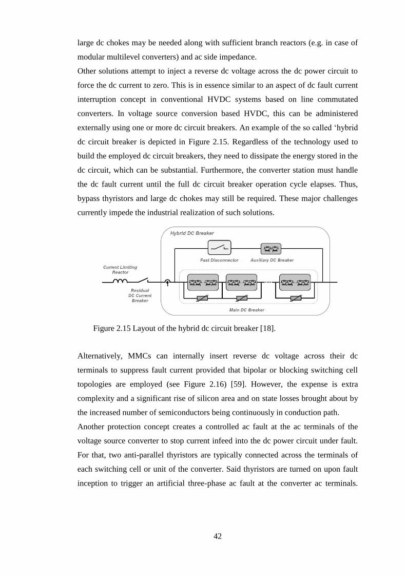
externally using one or more dc circuit breakers. An example of the so called ‘hybrid
dc circuit breaker is depicted in Figure 2.15. Regardless of the technology used to
build the employed dc circuit breakers, they need to dissipate the energy stored in the
dc circuit, which can be substantial. Furthermore, the converter station must handle
the dc fault current until the full dc circuit breaker operation cycle elapses. Thus,
bypass thyristors and large dc chokes may still be required. These major challenges
currently impede the industrial realization of such solutions.
Figure 2.15 Layout of the hybrid dc circuit breaker [18].
Alternatively, MMCs can internally insert reverse dc voltage across their dc
terminals to suppress fault current provided that bipolar or blocking switching cell
topologies are employed (see Figure 2.16) [59]. However, the expense is extra
complexity and a significant rise of silicon area and on state losses brought about by
the increased number of semiconductors being continuously in conduction path.
Another protection concept creates a controlled ac fault at the ac terminals of the
voltage source converter to stop current infeed into the dc power circuit under fault.
For that, two anti-parallel thyristors are typically connected across the terminals of
each switching cell or unit of the converter. Said thyristors are turned on upon fault
inception to trigger an artificial three-phase ac fault at the converter ac terminals.

43
This concept employs double the number of thyristors utilized in the bypass concept,
which is a drawback. The use of anti-parallel thyristor valves in a separate ac side
bridge rather than an anti-parallel thyristor pair in each switching cell or unit was
proposed. This, however, implies an extra non-modular converter structure is built in
the valve hall with dedicated snubbing and protective circuitry. There is an apparent
economic penalty in loss of modularity and modification of valve hall layout to
accommodate the extra converter. Said demerits impede industrial utilization of this
protection concept to date.
+
½V
dc
–½
Vdc
SM
HB
SM
SM
SM
HB
SM
SM
SM
Blocking HB
Semi full bridge
Full bridge
Double clamp SM
Figure 2.16 MMC cell (submodule) configurations for dc fault blocking.
2.2.4 The Alternate arm converter
One solution to overcome the dc fault vulnerability of the HB-MMC converter is to
employ so-called hybrid or mixed-cell design [60], [61]. Typically it is required that
a minimum of ½Vdc blocking is available in each arm by FB cells or any of the
blocking cells of Figure 2.16. In order to reduce the resulting conduction losses
penalty, so-called the alternate arm converter (AAC) has been developed in [62] to
achieve the required blocking capability with less amount of semiconductors. As
shown in Figure 2.17 each arm of an AAC comprises a stack of cascaded FB cells in

44
series with a switch array denoted a director valve. Each FB cell has three states;
‘+1’ state representing the switching state in which the cell produces +V, ‘–1’ state
representing –V output, and ‘0’ state representing shorted FB terminals (0V output).
FB
½Vdc
½Vdc
Figure 2.17 Structure of the Alternate arm converter
In steady-state, each arm of an AAC phase leg synthesizes one half of the
fundamental cycle. To synthesize the positive half cycle, the upper arm director
switch is turned on and all the FB cells switch sequentially – being initially at ‘+1’
state – to build a multilevel positive half of the sinusoidal ac voltage output.
Meanwhile, the lower arm director valve is off and lower arm FB cells are in ‘–1’
state. This implies the load current flows entirely in the upper arm while the positive
voltage half-cycle is synthesized. To synthesize the negative half-cycle of output
voltage and commutate current to the lower arm, the lower director valve is turned on
first to establish a closed path between all the FB cells of the phase leg and the dc
side to balance their energy (and cells voltages). The time period when both director
valves are on while FB cells of the phase leg are in state ‘+1’ is called the overlap

45
period. Following the overlap period, the upper director valve is turned off and the
lower arm FB cells switch sequentially to synthesize the negative half cycle.
The fact that the AAC employs FB cells enables it to generate an ac voltage peak
higher than the respective dc pole’s nominal voltage by exploiting the ‘–1’ state of
some FB cells. This capability is also available to the FB-MMC and hybrid MMC,
albeit at the expense of higher semiconductor area with respect to the AAC.
It is worth noting that the turn on and turn off of director valves occurs when the FB
cells of the phase leg are in the ‘+1’ and, theoretically, their aggregate voltage is in
small deviation from the dc link voltage. This implies that director valves switching
is under a near-zero-volt condition. Not only will this diminish their switching losses,
but also makes series connection of IGBTs in director valves less demanding in
terms of snubbing and gating requirements. Nevertheless, some sort of snubbing
might still be needed for uniform dynamic voltage sharing in each director valve.
As in the MMC, ensuring balanced cell voltages is essential to maintain output
voltage quality. A sorting mechanism (such as that of section 2.2.3.1) can be utilized
to keep the individual cell voltage ripple within a predefined band. However, for the
sorting mechanism to be effective, the net energy exchange for each stack of FB cells
in a half cycle needs to be minimized (ideally zero). The zero net energy exchange
condition means that the energy input to the stack from the dc circuit is equal to the
energy output to the ac circuit (assuming power flows into the ac circuit). This
condition implies that;
ac dcE E (2.24)
Assuming the ac pole current and voltage are;
( ) sin
( ) sin( )
ac s
ac s
i t I t
v t V t
(2.25)
Using (2.25) and the fact that the load current flows dominantly in each arm at a
time, (2.24) can be developed to;

46
2 2
0 0( ) ( ) ( )
2
dcac ac ac
Vv t i t dt i t dt
(2.26)
It follows from (2.26) that the zero next energy exchange of each FB cells stack over
a half cycle is;
4
2
dcVV
(2.27)
The condition in (2.27) implies that the peak ac pole voltage is 27% higher than the
dc pole nominal voltage. This is so-called ‘sweet spot’ in [62].
Requirement to operate near the sweet spot is a restriction as it implies that migration
from the sweet spot entails a longer overlap period to compensate for the resulting
voltage mismatch between the phase leg and the dc link. Should the overlap period
extend for a considerable part of the fundamental cycle, extra cells in each arm may
be required to keep the ac voltage transition during overlap so as to avoid output
voltage distortion. This defies the purpose of the AAC.
Although modulation methods have been proposed to relieve such a situation [63],
this remains a significant challenge for AAC utilization in high power and high
voltage applications. It is also important to note that unlike the MMC, the AAC
requires a dc-link capacitor to retain dc ripple within tolerances.
2.3 Isolated dc-dc converter designs
Galvanic isolation is inherently realized in ac grids by the use of the ac transformer
circuit. Since there is no other type of circuit capable of achieving effective galvanic
isolation at HVDC power and voltage levels, any dc-dc converter topology that
provides galvanic isolation between the connected dc circuits must utilize an ac
transformer. The ac transformer in this case will naturally undertake the voltage
stepping duty. However, ac transformers are bulky pieces of equipment at HVDC
power levels to the extent that transportation of the transformer to site is not an easy
task. This is one of the main reasons why normally HVDC LCC stations employ

47
three single phase power frequency transformers rather than a single three phase one.
Although a dc-dc converter is not bound to operate at the 50Hz power frequency, it
will be shown in Chapter 3 that the increase in power density obtained by raising the
fundamental frequency is limited by electrical and mechanical constraints.
Galvanic isolation may also be needed should the grounding arrangements of the dc
circuits to be connected impede safe or normal operation with a galvanic connection
in place. It may be important also to have galvanic isolation at dc nodes through
which bulky amount of power flows. In the case of a dc fault in one circuit, the other
circuit is naturally isolated and it becomes a matter of simple control to inhibit the
fault propagation. This capability will be explored in section 5.6.
The most fundamental design of an isolated dc-dc converter that offers some
potential for high power HVDC is the so called dual active bridge (DAB) [64] also
known as the front-to-front (F2F) dc-dc converter which is shown schematically in
Figure 2.18. In a DAB two three-phase dc/ac bridges are interfaced by an ac
transformer. The following subsections will evaluate the adequacy of some candidate
DAB designs reported in the literature for HVDC environment.
2.3.1 Two-level dual active bridge (2L-DAB)
Figure 2.19 shows a two-level dual active bridge with an array of series-connected
IGBTs in each arm to enable operation at high dc voltage. With the use of
fundamental frequency ranging from 250Hz to 1kHz in the ac link, the overall size
and weight of dc-dc converter can be reduced without significant sacrifice to its
efficiency. Traditionally, such two-level dual active bridges are operated in square
wave mode at fundamental frequency where each arm conducts for 180o (half a
fundamental period) [65], [66], [67], [68]. The phase shift (also known as the load
angle) between the voltage space vectors of both bridges is traditionally used for
power flow control [64]. Power flows from the side with the leading voltage space
vector. In this operating mode, self-commutated semiconductor devices in the DAB
tend to turn on and off at zero currents for much of the operating range (while anti-
parallel diodes are in conduction) as will be shown later in this section. Thus,
relatively low switching loss is achieved.

48
Figure 2.18 Generic three-phase DAB (F2F) dc-dc converter
Observe that the use of pulse width modulation can provide an additional degree of
freedom, which can be exploited to minimise the circulating reactive power in the ac
link. However, with the fundamental frequency range stated above, the use of high-
frequency pulse width modulation (PWM) must be precluded, because the increase
in switching losses and transformer losses are expected to outweigh the gains [69],
[70]. To avoid the shortcomings of the high frequency PWM, low-frequency
modulation scheme such as selective harmonic elimination (SHE) (e.g., with one
notch per quarter cycle) can be used to achieve the necessary control flexibility such
as ac voltage and reactive power control in ac link, especially during a dc fault.
However, with SHE the range at which inherent DAB soft switching at turn-on and
off is achieved will be reduced; hence, switching losses are expected to increase.
Figure 2.19 Schematic of a two-level DAB dc-dc converter design.

49
Theoretically, the phase a ac pole to ground voltages vap and vas of the bridges can be
expressed as in (2.28).
, , ..
, , ..
( ) sin( )
( ) sin( )
dcp
ap s
k
dcs
as s
k
Vv t k t
k
Vv t k t k
k
1 3 5
1 3 5
2
2 (2.28)
where, φ is the angle of vs relative to vp, and k = 2i + 1, i . Subscripts a, p, and s
refer to the turns ratio, primary, and secondary sides, respectively. If the medium-
frequency transformer is assumed to be lossless, and with transformer leakage
inductance referred to primary is Ls, the primary instantaneous current can be
expressed as:
( ) ( ) sin( ) sin( )dcp dcs
ap ap s s
k ks s
V Vi t i k t a k t k
L k k
2 2
1 1
2 210
2 2 (2.29)
The instantaneous power at the terminals of the primary converter expressed as
p (t) = 3 vap (t) iap (t) can be developed from (2.28) and (2.29). The average power
exchanged within DAB becomes:
sindcp dcs
DAB
ks s
V VP a k
L k
2 31
6 (2.30)
Equation (2.30) indicates that the medium-frequency transformer must be designed
to be able to transmit all the powers associated with significant low-order harmonics,
including that of the fundamental component. It also shows that the harmonic power
transfer diminishes with higher harmonic orders.
The salient drawbacks of the two-level DAB when utilized for HVDC applications
are:
1- The generation of square waves at each ac pole in the primary and secondary
bridges exposes the ac transformer insulation to intolerable dv/dt stresses
especially at high voltages. The large dv/dt also results in significant EMI.

50
2- To switch high voltages an array of many series connected IGBTs is needed
in each arm of the primary and secondary bridges. In addition to lack of
modularity, complex gating and snubbing circuitry is needed to ensure static
and dynamic voltage sharing among the IGBTs in each array.
3- Design of high power and high voltage transformers (handling several
hundreds of MWs at several hundreds of kVs) operating with square wave
voltage excitation even at lower medium frequency is a very challenging task
for the current state of the art.
4- Not suitable for high voltage transformation ratios as the semiconductors of
the low voltage side must handle high currents. For instance, for a = 20 and
the primary side dc current is 1kA, the secondary side dc current will be
20kA. Many semiconductor devices must be parallel connected to handle this
current (in addition to the series connection) which is not technically viable.
2.3.2 Multi-module DAB
To overcome the single large 2L-DAB dc-dc converter drawbacks, it has been
proposed to modularize the 2L-DAB station into many identical modules each
comprising a DAB dc-dc converter rated at a few kVs and a few MWs (see Figure
2.20). In connecting a high voltage dc circuit to a low voltage dc circuit through said
multi-module DAB, the dc links of individual DAB modules can be connected in
series, in parallel, or in series-parallel to achieve the required voltage transformation
ratio [71].
With this configuration, the ac transformer is modularized into a number of medium
voltage medium-frequency transformers which facilitates the ac link design and may
allow an increase in fundamental frequency with respect to the single large 2L-DAB.
Also, the flexibility of terminal connections facilitate the use of the multi-module
DAB for applications with high voltage transformation ratios. Furthermore, dv/dt
levels generated by medium voltage square waves are tolerable.

51
Figure 2.20 Schematic structure of s multi-module DAB dc-dc converter
An HVDC multi-module DAB design has been analysed in [72] in which each DAB
module is rated at 5kV. For that each arm in the primary and secondary bridges
comprises only two series connected 4.5kV forced commutation devices for a 100-
FIT steady-state voltage of 2.6kV. The force commutated devices can reportedly be
IGBTs or IGCTs (Integrated gate commutated thyristor) to handle high current
capacity. A case study on a 1.21GW multi-module DAB connecting a ±150kV dc
line at the primary side to a ±300kV dc line at the secondary side concluded that 120
DAB modules are required, each being 5kV, 10MW, and with a = 1. At the
secondary side the 120 modules will be connected in series while the 120 primary
side bridges are grouped into two parallel-connected 60-module groups. In each said
group, the 60 modules are connected in series.
The multi-module DAB dc-dc converter discussed in this subsection, and its
derivatives (e.g., single phase half bridge DAB configuration, single phase full
bridge DAB configuration) are expected to offer much better solutions at medium-
voltage when compared to the single large DAB dc-dc converter. The main
disadvantage associated with all multi-module dc-dc converters when employed
beyond medium-voltage are:
1- The use of multiple transformers and their requirement for high insulation
from real ground.

52
2- The need for an additional control layer to balance individual dc-link
capacitors at the primary and secondary sides
2.3.3 Resonant DAB designs
Figure 2.21 Generic structure of a resonant F2F dc-dc converter.
The F2F dc-dc converter topologies discussed in 2.3.1 and 2.3.2 can employ a
resonant tank in the ac link before or after the ac transformer with the main purpose
of extending the soft switching range. The resonant tank may also filter out some of
the high harmonics present in the square wave voltage wave produced by converter
bridges, which may offer advantages for transformer design. For a HVDC power-
level dc–dc converter to compete with the high efficiency standards set by ac power
transformers, extending the soft switching range may be an important aspect. This is
why soft-switched dc-dc converters have long been investigated in relation to
resonant converter topologies [73], [74], [75], [76], [77].
Several topologies have been reported in the literature where a series, parallel or
series-parallel resonant tanks have been introduced to the ac link. While adequate for
certain low and medium power applications, significant challenges impede the
scaling of most resonant designs to MV or HVDC high-power high-voltage range.
That is, resonant stages experience high internal voltage stresses and, hence, require
a special insulation design. Additionally, in practice inductance and capacitance
values drift owing to ageing and operating conditions. This leads to a drift of
operating points from the design target which reduces system efficiency and may
even impede proper operation.
In transformerless resonant designs, lack of galvanic isolation may be an additional
drawback. Such a resonant design employing no ac transformer in the ac link has

53
been reported in [78] and [79]. Figure 2.18 shows said converter which was
originally proposed as a high stepping voltage ratio multi-functional unit for use in
multi-terminal HVDC transmission systems with the ability to control power flow in
both directions and to prohibit the propagation of a dc fault beyond well-defined
sections of the HVDC network. However, high stepping voltage ratios may not be
practically viable since the semiconductor switch arrays connected in the low voltage
side bridge must be rated to withstand the peak voltage across the resonant tank
capacitor, which is 1.2 to 1.4 times the nominal rated voltage of the high-voltage
side. Generally, transformerless operation of F2F dc-dc converter designs might be
attractive in terms of cost and power density. However, it may lead to poor device
utilization.
The resonant converter design of Figure 2.18 is based on single phase concepts.
Consequently, there exists power ripple on both dc sides of the design of at twice the
resonant frequency which must be filtered. The presence of filter capacitors – subject
to their capacity and voltage – adds to the dc fault current levels. Like other non-
isolated dc-dc converter topologies (refer to section 2.4), pre-existing grounding
arrangements may preclude its connection to established dc links. These drawbacks
may preclude the utilization of this type of converter for HVDC applications.
Figure 2.22 A schematic of the non-isolated resonant dc-dc converter of [78].

54
2.3.4 MMC-based and AAC-based DAB designs
With regards to the drawbacks of scaling the 2L-DAB topology to HVDC voltage
and power levels, it is logical to consider the MMC design as an alternative for the
two-level bridges of the 2L-DAB. Replacing each two-level bridge of the 2L-DAB
with an MMC structure automatically eliminates the voltage sharing problem of the
series-switch arrays in each arm. The modular design ensures that each HB cell
capacitor clamps the primary IGBT in the cell (i.e., the bypassing IGBT).
Additionally, the ability of the MMC to shape the ac voltage output means that dv/dt
can be relieved by the adopted converter modulation technique. Also, if sinusoidal
waveforms are utilized in the ac link, the ac transformer design becomes an easier
task with respect to square wave excitation. Since the ac link is internal and not
connected to any ac grids, ac link frequency can be made higher than ac power
frequency. The higher frequency not only reduces the transformer core volume but
also constricts the intracycle energy swings of MMC arms and thus smaller cell
capacitances can be used, which results in a more compact MMC converter footprint.
When otherwise an ac grid connection is established in the ac link (see figure 19b),
operation at grid power frequency is mandatory and standard three winding ac power
transformers can be utilized [80] [81]. However, the overall station size becomes
roughly double the size of a standard MMC grid side converter station. This
configuration can also be viewed as though the point of common coupling (PCC)
between an ac grid and a dc line is interfaced to another dc line at a different voltage
level. Observe the use of three single phase transformers in each ac link at high
power levels.
In MMC-DAB design of Figure 2.19a, It was suggested in [81] that the ac currents
could be reduced, and hence ac losses, should the MMC bridges operate in over-
modulation (i.e., a modulation index m > 1). This could be realized when full bridge
cells constitute a portion of each MMC arm so as to produce an ac pole voltage vac >
½Vdc. Alternatively, the AAC [62] (refer to section 2.2.4) whose stable steady state
operating point is at a peak phase voltage of 127% the dc pole voltage can normally
realize the over-modulation. However, the expense of over-modulation would be
increased on-state losses in the MMCs due to the use of full bridge cells. The use of

55
the AAC instead of the MMC to achieve the over-modulation would sacrifice the
black start capability and current control capability during fault (refer to section
5.6.2.2).
MMC MMC DC LineDC Line
(a)
(b)
Figure 2.23 A schematic of an MMC based HVDC dc-dc converter station;
(a) with no interface to an ac grid, and (b) with an interface to an ac grid.
When each MMC of the F2F dc-dc converter operates in medium-frequency
multilevel sinusoidal modulation, the main attributes and drawbacks of this mode can
be summarized as:
Lower voltage stresses (dv/dt) on the isolation transformer compared to its two-
level equivalent.
Full modulation index range is available for voltage control in the ac link during
dc faults and for provision of black start of a dead dc networks following
blackout.
This mode does not fully exploit the active powers associated with significant
low-order harmonic voltages and currents; therefore, MMC-DAB operated in this

56
mode is expected to have lower power density compared to its two-level
equivalent.
This design may be unable to fully exploit soft switching available to 2L-DAB
configuration (only some of the devices will be turned on and off at zero current).
Although the use of a medium-frequency ac link of the MMC-DAB may lead to
compact design as previously stated, operation with low modulation index during
black start following dc network fault will increase the loading on the cell
capacitors. Thus, cell capacitance must be oversized to keep the cell voltage
ripple within tight limits and to avoid exposing switching devices to increased
voltage stress for the black start period.
2.4 Non-isolated dc-dc converter designs
At some HVDC nodes; for instance, a tap off connection, galvanic isolation may not
be crucial (e.g. should the tap off dc circuit be of the same topology as the main dc
line). Galvanic isolation, normally realized by a full-power ac transformer, may also
be sacrificed for economic reasons to achieve higher power density particularly for
offshore installations.
Several non-isolated dc-dc converter designs have been reported in the literature and
the most promising of them will be highlighted in this section. It is important to note
that the term ‘non-isolated’ is distinct from ‘transformerless’. As will be seen in this
section there can be a non-isolated designs that still incorporate an ac transformer. It
follows that a ‘transformerless design’ is one that does not incorporate any ac
transformers.
2.4.1 Non-isolated DAB designs
2.4.1.1 DC autotransformer
The dc autotransformer proposed in [82] and shown in Figure 2.24 only converts part
of the total dc power exchange between the two dc sides into ac power to be
transferred between converter bridges through the coupling ac transformer. An
asymmetric monopolar arrangement of this design is shown in Figure 2.24 and it can
57
be viewed as a non-isolated DAB design as the power flow through the coupling
transformer is also controlled by the magnitudes and phase shift between the voltage
space vectors of individual bridges.
In the asymmetric monopolar arrangement of Figure 2.24 comprising an upper
bridge and a lower bridge, the part of dc power converted into ac power Pac is;
Pac = IH (VH – VL) (2.31)
where IH, VH, and VL are the high voltage dc side current and voltage and low voltage
side voltage, respectively. Pac is eventually fed to the low-voltage dc side through the
lower bridge. The remaining part of the dc power is transferred directly to the dc side
of the lower bridge using the common mode currents of the upper bridge (dc
component of the arm currents). Thus, the MVA rating of the coupling transformer in
the ac link is reduced or even halved when VH : VL = 2:1 or (VH– VL):VL = 1:1. With
the power flow shown by direction of the dc currents in Figure 2.24 and IdH and IdL
being the magnitudes of common mode currents in the arms of the upper and lower
converters, respectively, the dc link current of the lower bridge (IL) is;
IL = 3( IdH + IdL ) (2.32)
where IdH = ⅓IH and;
IdL = ⅓ IH (VH – VL) /VL (2.33)
Observe that IdL is set by the ac power that is transferred through the ac link. For
example, when VH = 2VL, IdH = IdL = ⅓IH and IL = 2IH, and these indicate that the dc
autotransformer is expected to have higher efficiency compared to F2F equivalent.
The reason is that the semiconductor switches of the lower bridge experience half the
current stresses relative to that of an equivalent F2F connection (at a conversion ratio
of 2).
However, for the dc autotransformer to block dc fault propagation from one dc
circuit to the other, large number of FB cells needs to be inserted in the outer arms in
order to block fault current flow. This represents a major weakness as it compromise

58
the high efficiency that could be achieved when only HB cells are employed beyond
a certain conversion ratio. Additional problem of the asymmetric auto dc transformer
of Figure 2.24 is that it exposes both windings of the coupling transformers to
continuous high dc bias. This situation is avoided when dc autotransformer is
reconfigured for symmetrical dc circuit topology where transformer windings
experience no dc voltage stress.
A multiport topology of the dc autotransformer has been recently presented in [83]. It
exhibits the same operating principles of the two-port dc autotransformer explained
above while using multiple ac transformers. In conclusion, so-called dc
autotransformer designs may achieve higher power density and less amount of
semiconductors with respect to equivalent F2F dc-dc converters for low voltage
(transformation) ratios. It is also limited to cases where galvanic isolation is not a
prerequisite.
Figure 2.24 Generic three-port dc-dc converter representation

59
2.4.1.2 DAB dc tap-changer
A design of a multi-ratio MMC-based DAB design has been reported in [84]. This
design resembles an ‘ac tap-changer’ in the sense that it offers more than one voltage
transformation ratio in a single design.
This non-isolated dc-dc converter may also employ a 1:1 ac transformer for galvanic
isolation. In either case, each MMC bridge of the DAB can be used to achieve a
‘voltage elevation’.
The operating principle of each MMC bridge here is different from standard MMC.
Each cell in the primary side MMC must be rated to the primary dc voltage input if
voltage elevation is required. Furthermore, all cells must be bipolar (i.e., a full bridge
cell). Each MMC is composed of two phase legs to produce a single phase ac voltage
obtained between the two ac poles of the primary MMC bridge.
Voltage elevation is realized utilizing the ‘–1’ state of FB cells. In the example of
Figure 2.25 where there is three FB cells per arm, the ac voltage vac can be made five
multiples of the dc input magnitude (i.e., an elevation ratio of 5) with the following
cell arrangement:
For the first half cycle: The upper arm in phase leg 1 and the lower arm of
phase leg 2 have all cells in ‘+1’ state. The lower arm of phase leg 1 and the
upper arm of phase leg 2 each have two cells in ‘–1’ state and one cell in ‘0’
state.
For the second half cycle: The lower arm in phase leg 1 and the upper arm of
phase leg 2 have all cells in ‘+1’ state. The upper arm of phase leg 1 and the
lower arm of phase leg 2 each have two cells in ‘–1’ state and one cell in ‘0’
state.
This switching sequence produces a two-level ac output of magnitude 5Vdc. Voltage
elevation can also be achieved through the secondary MMC bridge (the ac
transformer is present only for isolation). Here, HB cells are sufficient and each cell
is to be rated at the peak ac voltage across the two ac pole. For instance, for the

60
secondary bridge of the same DAB dc-changer to elevate the voltage by a ratio of 5
(i.e., an overall voltage elevation of 25 in the DAB dc tap-changer), the following
cell arrangements are needed in the secondary MMC:
For the first half cycle: The upper arm in phase leg 1 and the lower arm of
phase leg 2 have all cells in ‘+1’ state. The lower arm of phase leg 1 and the
upper arm of phase leg 2 each have two cells in ‘+1’ state and one cell in ‘0’
state.
For the second half cycle: The lower arm in phase leg 1 and the upper arm of
phase leg 2 have all cells in ‘+1’ state. The upper arm of phase leg 1 and the
lower arm of phase leg 2 each have two cells in ‘+1’ state and one cell in ‘0’
state.
The primary or secondary bridge can be operated in two-level (square wave) mode
when no elevation is required. In either case, power flow is governed by the phase
shift between the respective voltage space vectors.
Vdc
Vdc
Vdc
Vdc
5Vdc
5Vdc
State ‘0’ State ‘+1’ State ‘–1’
25Vdc
1 2 1 2
Primary Secondary
Figure 2.25 A non-isolated dc tap-changer DAB with an overall voltage elevation ratio of 25 from primary to secondary.

61
It has been shown in [84] that the ac pole currents are shared between the arms of
respective phase legs and that cell energies and capacitors voltage ripple can be
managed by the conventional sorting algorithm (see 2.2.3.1).
Despite the flexibility offered by this tap-changer-like design, its utilization is likely
limited to medium voltage applications. The underlying reason is that each FB cell in
the primary bridge has to be rated to the primary side dc voltage to achieve any
voltage elevation. Similarly, for the secondary bridge to elevate the voltage each HB
cell must be rated to the peak ac link voltage.
2.4.2 Transformerless dc-dc converter designs
A number of transformerless dc-dc converter designs have been reported for
utilization in HVDC applications. While these designs realize voltage stepping
without using any ac transformer circuit, they employ chain-links of FB or HB
submodules.
Two transformerless dc-dc converter designs will be considered here. The two
designs are, however, derived from one concept. That is, a dc/ac VSC converts the dc
voltage to ac voltage. In an asymmetric monopolar arrangement the produced ac
voltage would be offset by the magnitude of the low side voltage. A filter circuit is
then used to filter the alternating component of the VSC output voltage. In bipolar or
symmetric monopolar dc circuit arrangements, one such dc-dc converter
configurations is connected between a dc pole and ground (see Figure 2.26).
The salient distinction between the two considered designs is the internal structure of
the VSC stage and filter type. In the first design, denoted the single-stage modular
multilevel dc-dc converter, the VSC buck stage is an MMC and the filter circuit
comprises passive components. In the second design, denoted the hybrid cascade dc-
dc converter, the VSC buck stage is a conventional two-level (six-pulse) bridge and
the filter circuit comprises chain-links of FB or HB submodules.

62
Filter
CircuitVH
VL
Filter
Circuit
VH VL
Filter
Circuit
(a) (b)
Figure 2.26 Generic transformerless dc-dc converter design; (a) the
asymmetric monopolar building block, and (b) the symmetric monopolar
configuration.
2.4.2.1 The single-stage modular multilevel dc converter (MMDC)
Several version of the MMDC has been presented in [85]. The same concept has
been proposed and developed concurrently in [86] and [87] although under a
different name. Despite the different approaches followed in the analysis and
classification of each of the proposed topologies in [85], [86], and [87], these
topologies are all slight variations of the same concept.
Figure 2.27 depicts so-called push-pull MMDC proposed in [85] where standard
MMC phase legs can be used to generate an alternating voltage waveform. Due to
the asymmetric arrangement (lower dc pole represent ground potential), a dc offset of
VL is present. The operating principle utilizes the coupled inductors L1 to limit the
circulating current responsible for regulating submodules energy levels while the
coupled inductors L2 act as a filter such that the low side dc voltage and current
ripple are within tolerances.
Figure 2.28 shows MMDC arrangement of [86] and [87] which can be viewed as the
three phase symmetric monopolar version of the push-pull MMDC. For expedience,
the former will be denoted the symmetric MMDC. The symmetric MMDC generates
output voltages that contain ac plus dc bias at the ac poles of the upper and lower
MMC bridges with respect to ground. Therefore, it similarly requires output filter
inductance and capacitance to attenuate the fundamental ac voltage components from
each phase voltage when measured relative to ground; otherwise, pole-to-ground dc
voltage of the low-voltage side will be modulated at the fundamental frequency used
to exchange power between converter arms.

63
Figure 2.27 Design of the push-pull single stage modular multilevel dc-dc converter (MMDC)
In the considered MMDC topologies, the required inductor filters are expectedly
large. For instance a case study in [87] concluded that a filter inductance Lf = 990mH
is needed for a ±17.6kV 40MW system. In [72] detailed design of the push-pull
MMDC version was carried out and it was concluded that filtering the ac
components will necessitate a similar amount of magnetics as in an equivalent multi-
module DAB dc-dc converter. It was reported also in [88] that a third version
denoted the tuned-filter MMDC proposed in [85] requires even more magnetics than
an equivalent push-pull MMDC.
With respect to dc fault isolation, the MMDC concept does not naturally inhibit the
propagation of dc faults without the addition of extra semiconductors (FB
submodules in the outer arms). Even when the dc blocking capability is ensured by
sufficient FB blocking submodules, converter semiconductors may be exposed to
excessive current stresses due to the large filter inductances in the fault current path.
A study of the MMDC behaviour under different dc fault scenarios is mandatory for
better evaluation of the concept; this is still not reported in the literature.

64
Given the above reasons, the MMDC concept may not be competitive in medium and
high-voltage applications.
Figure 2.28 The symmetric monopolar MMDC design of [87].
2.4.2.2 The hybrid cascaded dc-dc converter
Figure 2.29 shows three configurations of said second high-voltage transformerless
dc-dc converter design (HCDC) and recently proposed in [89]. The HCDC comprises
a six-pulse bridge whose ac poles are connected to chain-links of submodules. For an
asymmetric monopole design, it can be observed from Figure 2.29 that the six-pulse
bridge can be connected either between the high voltage dc pole and ground
(configuration HCDC1), between the low voltage dc pole and ground (configuration
HCDC2), or between the high and low voltage dc poles (configuration HCDC3). The
chain-links are connected to the low voltage dc pole in HCDC1, to the high voltage
pole in HCDC2, and to ground in HCDC3. In all configurations, each chainlink is
connected in series to a current limiting inductor Ld.

65
In HCDC3 the HB chain-links of each limb are rated to full dc voltage of the high
voltage side in order to be able to switch alternatively between VdcH and VdcL using
series connected IGBTs of the six-step bridge (e.g., S1 and S4 for phase ‘a’) without
exposing cell capacitor and switching devices of individual HB cells to excessive
voltage stresses. The series device IGBTs of the high and low voltage sides must be
rated to withstand VdcH – VdcL, which is attractive from semiconductor conduction
loss point of view. In HCDC3, the HB cell capacitors clamp the voltage across the
submodule switching devices during abrupt switching between VdcH and VdcL. The
main drawback of HCDC3 is that during dc fault on its high-voltage side, the
freewheeling diodes of the six pulse bridge – depending on their polarity – as well as
primary switches of the HB cells will be exposed to high current stresses.
In HCDC2, the dc link of the six-pulse bridge is the high-voltage side; therefore,
chain-links submodules in the low voltage side must be of full-bridge design. In this
arrangement, the FB chain-link of each limb generates square waveform bipolar ac
voltage of the magnitudes given in (2.34) in order to generate a ripple free (filtered)
dc voltage with magnitude of VdcL at the low voltage side.
1
4
,
,
dcH dcL
dcL
V V S ON
V S ON
(2.34)
This means the series connected switching devices of the six-pulse bridge must be
rated to block full dc voltage of the high voltage side.
In HCDC1, the dc link of the six-pulse bridge is the low voltage dc side. Thus, the
HB cells are sufficient in the chain-links for steady state operation instead of FB
cells. The underlying reason is that each limb needs to generate only a unipolar
voltage waveform to boost the low side dc voltage as given in (2.35). In this
scenario, the chain link of each limb must be able to support full dc voltage of the
high-voltage side.

66
(a)
(b)
(c)
Figure 2.29 Configurations of the hybrid cascade dc-dc converter (HCDC):
(a) HCDC1, (b) HCDC2, and (c) HCDC3.

67
1
4
,
,
dcH dcL
dcH
V V S ON
V S ON
(2.35)
Figure 2.30 Generic three-port dc-dc converter representation
Overall, the HCDC offers promise for dc-dc conversion applications insensitive to
galvanic isolation. However, in addition to the lack of galvanic isolation, conduction
losses in HCDC designs are not yet reported. Also, the amount of extra
semiconductors required to enable HCDC designs to effectively block the
propagation of dc faults between both dc circuits and the consequent conduction loss
penalty are yet to be established for the three designs of Figure 2.29 with
consideration of all possible dc fault scenarios and dc circuit topologies. Figure 2.30
depicts a symmetric monopolar dc circuit configuration where both pole-to-ground
and pole-to-pole dc faults are possible and need to be studied.

68
2.5 Desirable Features in Candidate HVDC-DC Converter
Considering the discussion presented along previous sections of this chapter, the
following generic set of desirable features can be defined for a candidate dc-dc
converter for use in multi-terminal HVDC networks:
A suitable compromise between capital cost, footprint (power density), and
losses (running cost). The right compromise is to be set on case-by-case
basis, depending on the voltage and power transfer levels involved and the
nature of the application (e.g. onshore or offshore)
Soft switching is an important asset whether over part of or the full range of
operating points.
Capability to ride-through dc side faults whether temporary or permanent. No
less important is the capability to provide circuit breaking functions by
blocking dc fault propagation from the faulted dc side to the healthy dc
side(s).
Flexibility to utilize the available power electronics components to administer
power flow control and dc voltage regulation duties.
Galvanic isolation is favourable particularly for connection of dc lines of
different ground point arrangements.
Galvanic isolation is important for designs involving two or more dc/ac
converters with an intermediate ac link. The introduced ac voltage matching
(voltage stepping) capability is essential to minimize reactive power
circulation in the ac link or otherwise avoid poor utilization of installed
semiconductors at the high voltage side.
Avoiding high fundamental frequency operation. This in part is due to the
slower nature of high voltage power electronics devices. Furthermore, the
reduction in size and weight of the coupling ac transformer (if present)
beyond a certain limit is impeded by the physical clearances at high voltage
levels. Also, iron losses and parasitic phenomena are limiting. Some of these
constraints are, however, relieved in multi-module designs.

69
The voltage slopes (dv/dt) resulting from switching actions within the dc-dc
converter must be fully controllable particularly when a coupling ac
transformer is utilized at such high voltage levels.
The capability of black start is a valuable asset. For this purpose, it is
desirable that a candidate design is capable of modulation index control over
a wide range. This is also helpful for power flow control as well as handling
faulty conditions and power flow disturbances.
Scalability to high voltages without excessive complexity, compromising
controllability over dv/dt, or reducing reliability.
Modularity, full or partial, of the dc-dc converter structure is an important
economical aspect. In modular designs, internal fault handling is also
improved resulting in higher reliability.
Employing resonant tanks is not encouraged due to the value drift problem of
passive components by aging. Furthermore, some resonant designs feature
high internal voltage stresses which may render insulation design
uneconomic at high voltage.
In light of these design guidelines, the following chapters will propose a number of
converter designs aiming at fulfilling (at least) most of the mentioned criteria. The
proposed designs will be analysed and validated at both device and system levels.
Also, some design aspects will be discussed.
In recognition of the challenges presently involved in building a high voltage and
high power dc-dc converter of the above technical merits while retaining an
attractive compromise between cost and footprint, the primary aim of the present
thesis is more of broadening the horizon in a quite fresh field of research than
responding solely to pressing industrial needs.

70
Chapter 3 Chapter 3
Dual Active Bridge Structure Based on the Quasi Two-
Level Converter
This chapter introduces the operation of DAB (or F2F) dc-dc converters with
trapezoidal voltage waveforms in the ac link. The operation of MMC structure with
said trapezoidal (quasi two-level) voltage waveforms is studied. Various design and
operation aspects are studied in depth supported with numerical simulations and
experimental validation, where appropriate.
In chapter 5, the isolated dc-dc converter structures proposed in this chapter and in
chapter 4 will be compared and will be judged in Chapter 7 against the set of
desirable criteria put forward in 2.5.
3.1 Trapezoidal operation of the DAB dc-dc converter
It has been concluded in chapter 2 that operation of the DAB dc-dc converter in two-
level mode impedes scalability to higher voltage ranges primarily due to the high
dv/dt stress impressed on the coupling ac transformer insulation as well as the
complexity and low reliability associated with series-switch strings. A possible
alternative that has been discussed is modularising the DAB converter into so called
multi-module DAB. Alternatively, sinusoidal voltage waveforms could be adopted in
the ac link to allow the utilization of the MMC concept with all its advantages.
However, the resulting footprint of a DAB station harbouring two front-to-front
MMC converters is too large, as mentioned in Chapter 2, even with operation at
higher fundamental frequency. Additionally, soft-switching capabilities of a DAB
structure are not effectively utilized under sinusoidal operation of MMCs.
In order to circumvent the shortcomings of the two-level operation of DAB dc-dc
converters and relief the footprint penalty arising from the use of MMCs with
sinusoidal ac voltages, operation of DAB with trapezoidal ac waveforms in the ac
link is introduced herein. In this mode, each of the two MMCs in a DAB synthesizes

71
a stair case approximation of a three phase trapezoidal voltage waveform at the
respective ac poles. As will be detailed along this chapter, the operation of a MMC-
based DAB with trapezoidal ac voltage waveforms offers a better utilization of the
available dc voltage at each dc side. Additionally, this mode of operation offers
relatively low switching and conduction losses. It requires relatively less installed
semiconductor power and smaller footprint. Also, operation with switching
sequences which are distinct from conventional MMC’s complementary switching is
possible. Due to this structural and operational distinction to the conventional MMC
operated in sinusoidal mode, the MMC under trapezoidal operation will be denoted
‘the quasi two-level converter (Q2LC)’ henceforth for expedience.
Figure 3-1 depicts the generic structure of a Q2LC-based F2F dc-dc converter and
the staircase approximation of the trapezoidal ac waveform as synthesized by each
Q2LC ac pole. In Figure 3-1, Td is the dwell time spent in each intermediary voltage
level between the two dominant voltage levels of the trapezoidal ac waveform, T is
the fundamental ac period, a is the coupling ac transformer turns ratio, and Vdcp and
Vdcs are the primary and secondary dc voltages, respectively.
Only three phase DAB structures are considered in this thesis. In a three phase DAB
ac link, one three phase transformer could be utilized, or alternatively three single
phase transformers connected in a Y-Y, Y-∆ or ∆-∆ configuration [90]. As in typical
HVDC station, the ac link of a high voltage high power DAB would normally be
composed of single phase transformers to facilitate transportation.
In an DAB ac link with a Y-Y coupling transformer configuration, the phase to
neutral voltage (winding voltage) at each of the primary and secondary sides may be
a two-step trapezoidal ac waveform or a six-step trapezoidal ac waveform, depending
on the potential of the neutral point with respect to the respective dc link midpoint
voltage.
The two-step three phase trapezoidal ac waveforms are produced as shown in Figure
3- 2b when neutral points are connected to respective dc link midpoints. A dc-link
split capacitor bank is required to establish this connection even if a dc side filter is
not required for the converter operation. Figure 3- 2 depicts the generic DAB
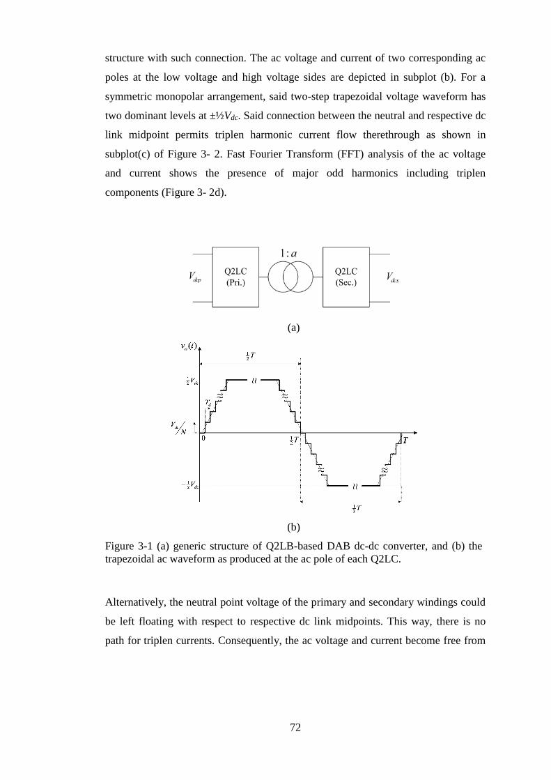
72
structure with such connection. The ac voltage and current of two corresponding ac
poles at the low voltage and high voltage sides are depicted in subplot (b). For a
symmetric monopolar arrangement, said two-step trapezoidal voltage waveform has
two dominant levels at ±½Vdc. Said connection between the neutral and respective dc
link midpoint permits triplen harmonic current flow therethrough as shown in
subplot(c) of Figure 3- 2. Fast Fourier Transform (FFT) analysis of the ac voltage
and current shows the presence of major odd harmonics including triplen
components (Figure 3- 2d).
(a)
(b)
Figure 3-1 (a) generic structure of Q2LB-based DAB dc-dc converter, and (b) the
trapezoidal ac waveform as produced at the ac pole of each Q2LC.
Alternatively, the neutral point voltage of the primary and secondary windings could
be left floating with respect to respective dc link midpoints. This way, there is no
path for triplen currents. Consequently, the ac voltage and current become free from

73
triplen components (Figure 3-3). This voltage waveform is called six-step trapezoidal
waveform. A six-step waveform has dominant levels at ±⅔Vdc and ±⅓Vdc.
It has been shown in [91] that six-step voltage waveforms produce a flux pattern in
the ac transformer core which is very close to that of sinusoidal excitation (Figure 3-
4). This conclusion has been verified by measurements carried out on 0.18 mm thick
laser-processed grain-orientated steel in an Epstein frame for up to 10 kHz excitation
frequencies with and without loading. Although further research is required to verify
these findings on a high power design, it can be concluded that six-step excitation
shows more promise for iron losses of DAB ac link transformer which are
comparable to these of sinusoidal voltage excitation. This is likely to facilitate the
design process of the ac link. However, this is traded for a floating neutral point
voltage as well as higher peak ac pole current as noticed from Figures 3-2 and 3-3
which are generated from an illustrative simulation case of a 600MW DAB dc-dc
converter connecting two symmetrical monopolar dc lines at ±150kV and ±320kV.
Only operation of the DAB dc-dc converter with six-step trapezoidal ac-link voltages
will be considered henceforth.
In general, the power density can be increased with a higher ac frequency, leading to
reduction of the volume and weight of the coupling transformer stage. It has been
shown in previous research that tenfold increase of power density is attainable by
increasing frequency from 50Hz to 1000Hz without compromising design reliability
[91][65].
However, as has been pointed out in chapter 2, beyond a certain limit, the relation
between power density and frequency becomes non-linear due to the limitations set
by the physical clearance required for mounting large transformer bushings as well
as creepage distance restrictions.
The studies conducted henceforth assume a fundamental ac link frequency in the
range of 250Hz to 500Hz. The primary reasons for such a choice are:

74
(a)
(b)
(c)
(d)
Figure 3- 2 DAB dc-dc converter with two-step trapezoidal ac-link voltage (a)
generic structure, (b) zero sequence current of the high voltage side, (c) transformer
windings voltage and current of one phase, and (d) FFT analysis of the voltage and
current of one ph phase, and (d) FFT analysis of the voltage and current of one phase
(low voltage side)

75
(a)
(b)
Figure 3-3 DAB dc-dc converter with six-step trapezoidal ac-link voltage (a)
transformer windings voltage and current of one phase, and (d) FFT analysis of the
voltage and current of one phase (high voltage side)
1- Given current state of core material technology [91], operation at such
frequency range may allow some of the low order harmonics contribute to the
power transfer process in addition to the fundamental component. This might
be feasible with the use of suitable materials such as laser-processed grain-
orientated steel with fine thickness. For instance, if the core material allows
power transfer up to 2kHz, this implies the 5th and 7th harmonic components
(in addition to 3rd component if operated with two-step trapezoidal
waveforms) engage in power transfer when the fundamental frequency is
250Hz.
2- Mitigate losses incurred by parasitic components. Primary parasitic
components are: inter-winding capacitances (between windings), and intra-
winding capacitances (between turns of same winding), and capacitances

76
between windings and the core or shields. These parasitic capacitances lead
to oscillations and ringing at high voltage slopes (high dv/dt) and at higher
frequencies.
Figure 3-4 Comparison of ac transformer excitation with sinusoidal and six-step
voltage waveforms. (middle) B-H curves, and (right) Magnetic flux density in
transformer core over a fundamental period [91].
It is worth noting that the use of six-step trapezoidal waveforms implies the absence
of high order triplen harmonics, which also relieves said parasitic losses.
Additionally, the slopes of trapezoidal waveforms can be further manipulated to
eliminate some other high order harmonics.
Consequently, engineering the core in terms of shape, dimensions, and material to
suit the indicated frequency range (which is about a 5 to 10-fold the frequency of a
conventional ac power transformer) and with six-step trapezoidal excitation is
potentially a relatively easier task. Especially that there exists no special insulation
design requirement for extra DC stress (as the case with HVDC grid side terminal ac
power transformers).
Detailed studies are needed to better evaluate the above claims with regards to
coupling transformer design. This is a topic for future research as pointed in Chapter
7 and is not a point of focus in this thesis due to the associated complexity and
length, as well as lack of suitable experimentation tools. Instead, the primary aim of
the thesis henceforth is to investigate the aspects, merits and, demerits of trapezoidal
operation of high power high voltage dc-dc converters with respect to power
electronic components structure, design, and operation.

77
3.2 The Quasi Two-level Converter
3.2.1 Synthesis of the trapezoidal voltage waveform
Each MMC in the DAB dc-dc converter of Figure 3-1a is operated in a quasi two-
level (trapezoidal) mode where the cell capacitors of each phase arm are in the
conduction path for short time intervals only to facilitate orderly stepped transitions
between voltage levels ½Vdc and –½Vdc through intermediate cell voltage levels
(see Figure 3-1b). The dwell time Td spent at each intermediate voltage level is
sufficiently small to reduce the energy storage requirement per cell capacitor for a
given voltage ripple, and must remain compatible with the switching speed of high-
voltage insulated gate bipolar transistors (IGBTs). Also, the value of Td must be
large enough to avoid unacceptable voltage derivative dv/dt stresses and eliminate
higher harmonics from the output voltage waveform.
Figure 3-5 Generic structure of a single phase leg quasi two-level converter.
In this manner, each phase of the Q2LC generates a step approximation of a
trapezoidal ac voltage with pre-defined volytage steps equal to one cell capacitor
voltage (Vdc/N), with a total transition time Tt between the two dominant voltage
levels ½Vdc and –½Vdc given as in (3-1).
Tt = (N – 1) Td (3-1)

78
where N is the number of cells per arm. The proposed trapezoidal mode exploits the
structure of the modular multilevel converter to realize a converter that presents a
low dv/dt akin to true multilevel modulation but with a reduced footprint due to
relieved cell energy storage requirement. The dwell time at each cell voltage level is
selected sufficiently small so that the total transition time 2(N – 1) Td per cycle is
much smaller than the fundamental period time span T. During the non-transitional
times, where the ac voltage is at either of the two dominant voltage levels, the ac
poles of the Q2LC will be connected to the positive or negative rails. This implies
that the Q2LC exhibits some of the operation characteristics of a two-level converter.
That is, current flows separately in each arm per phase leg for an interval T2L of the
fundamental half-cycle, where T2L is expressed as in (3-2).
12 2
1L dT T N T (3-2)
Only during brief periods when the cell capacitors are successively switched, both
upper and lower arms of each Q2LC phase leg share ac pole current as in true
multilevel operation of the MMC. Therefore, the proposed trapezoidal operation
mode eliminates the common-mode components normally present in the arm currents
of a conventional MMC except during voltage transition intervals Tt.
For a deeper understanding of the Q2LC operation aspects, it is useful to view each
phase arm as a string of series-connected IGBTs, representing the power path, where
each power IGBT is shunted by an auxiliary circuit comprising an auxiliary
IGBT/diode pair and a capacitor. In Figure 3-5, the power IGBT/diode pair in each
half bridge (HB) cell is depicted in bold line. The auxiliary circuit normally acts as
an active soft voltage clamp ensuring equal dynamic and static voltage sharing
between all the power IGBTs of an arm. While an ac pole reverses phase voltage
polarity, an appropriate switching pattern permits the auxiliary circuit of each power
IGBT to act also as an energy buffer, as explained earlier.
For uniform intermediary voltage steps, all the auxiliary capacitor voltages must
remain near equal. Since each arm of a two-level converter (or a MMC) must block
the dc-link voltage, the required voltage level of each auxiliary capacitor is ideally

79
Vdc / N. The Q2LC controllers must ensure balanced capacitor voltages within an
acceptable band around this set-point.
With stepped voltage transitions introduced between –½Vdc and ½Vdc, the steady-
state voltage seen by each arm in Figure 3-5 is:
Vx = Vdc (1 – NYon / N) (3-3)
where subscripts and . Symbols U and L refer to the upper and lower
arms, respectively. In (3-3), NYon is the number of inserted auxiliary capacitors in the
complementary arm. For modelling purposes, NYon may be expressed as in (3-4).
0,1... 1
0,1... 1
( ), ( 1)
( 1) ½( )
( [½ ]), ½ ½ ( 1)
0, ½ ( 1)
, 0,1,2,...., ,
d o o d o
i N
d o o
Yon
d o o d o
i N
d o o
o Y
s
u t iT t t t N T t
N N T t t T tN t
N u t T iT t T t t T N T t
T N T t t T t
kwhere t k Y U L
f
(3-4)
Substituting (3-4) in (3-3) gives the arm voltage VX as a time function. In the Q2LC,
an ac pole is tied to one of the dc rails when . Stepped voltage
transitions occur when 1 ≤ NYon < N in a staircase approximation of a trapezoid.
Since the voltage across both arms of a phase leg at any instant equals the dc-link
voltage, maintaining the capacitors voltages around the Vdc / N set point intuitively
requires that the total number of inserted auxiliary capacitors in both arms at any
instant satisfies (3-5).
NUon + NLon = N (3-5)

80
This entails a complementary switching pattern of both arms of each phase leg.
However, the Q2LC operating mode permits the use of a third cell switching state –
denoted idle state – where both the power and auxiliary IGBTs are in off-state
(Figure 3-5). Possible switching sequences employing this switching state are able to
achieve proper operation with NUon + NLon < N, as will be shown in section 3.2.4.1.
The single-leg Q2LC output voltage expression is given in (3-6). Equation (3-6)
holds as well for switching sequences where the idle cell state is employed, provided
the arm having idle cells is not used to calculate (3-6).
( ) ( )1 1( )
2 2
Uon Lon
o dc dc
N t N tv t V V
N N
(3-6)
3.2.2 Grouping of half bridge cells in a Q2LC
The high voltage levels in HVDC applications often require hundreds of cascaded
HB cells per phase arm so as to block the dc link voltage. While this is customary in
MMC design, sequential switching of hundreds of cells in a Q2LC arm may pose a
computational challenge for the controllers if cell voltage balancing algorithm
requires measurements of individual cell voltages during the ac pole voltage
transition. This is due to the short span of voltage transition times of synthesized
trapezoidal voltages (Tt is in the range of a few tens to a few hundreds of
microseconds). Nonetheless, a suitable voltage balancing algorithm may be tailored
to circumvent this drawback.
Additionally, sequential switching of hundreds of cells in each arm of a Q2LC at Td
time steps may result in the interval Tt constituting a significant portion of the
fundamental period, which leads to a reduction of the fundamental ac voltage
component and requires extra energy storage capacity available to cells to avoid
violation of cell voltage ripple tolerances. Theoretically, the dwell time Td may be
minimized to reduce Tt. However, the minimum value of Td is dictated by the
switching delays of switching devices, and must not result in a violation of tolerable
dv/dt stress.
In a possible solution to the above challenge, the Q2LC is not required to produce a
trapezoidal ac voltage waveform of N+1 voltage levels when N low-voltage cells are

81
installed per arm. Instead, each number of low-voltage cells per arm can be
considered to form a ‘subgroup’ by being controlled to switch simultaneously. A
low-voltage cell here is a cell which employs a single 1.7kV, 3.3kV or 4.5kV
IGBT/diode pair in the power and auxiliary circuits of the cell.
By grouping cells into subgroups, the number of output ac voltage levels can be
reduced from N + 1 to Ns + 1 (Figure 3-6) where;
sNN
n
(3-6)
and n is the number of cells per cell subgroup. The minimum value of Ns, which
corresponds to the upper value of n, is subject to the permissible dv/dt levels. In such
a case, each subgroup will be composed of n HB cells which are effectively series-
connected. Equal static and dynamic voltage sharing in a subgroup is assured by the
auxiliary capacitors. Gating delays may cause slight voltage imbalance between
capacitors of the sub-group. To avoid complex gate drive circuitry, the employed
capacitor balancing technique will need to address individual cell voltages of the arm
rather than subgroups aggregate voltages.
In curtailing the number of ac pole voltage levels to Ns + 1, the main Q2LC design
constraint can be set to the selection of N, Td, and ωs (the fundamental angular
frequency) values to control the dv/dt level at a minimum drop in fundamental
voltage magnitude and with minimum cell capacitance. This issue will be revisited
several times along the thesis.
As an alternative to cell grouping, medium voltage half-bridge cells can be employed
in the Q2LC rather than low-voltage cells. A medium voltage cell is a cell where
IGBT/diode pairs are series connected in the power path and auxiliary path to block a
higher voltage, as in the cascaded two-level converter of ABB [53] (refer to 2.2.3). In
this case, N of (3-6) becomes the total number of power IGBTs per arm and n
denotes the number of series power IGBT modules in the cell.

82
Whether low-voltage or medium voltage cells are employed in the Q2LC, a suitable
redundancy margin in terms of cell numbers and voltage ratings is mandatory for
uninterrupted and balanced operation of the Q2LC with faulted cells.
Figure 3-6 Effect of cell grouping on the ac pole trapezoidal voltage and transition
time in a Q2LC; (left) no grouping, and (right) cells grouped.
3.2.3 Analysis of the trapezoidal ac voltage
It may be clear to the reader at the is point that, in a Q2LC design, the number of
cells per arm N (or number of levels Ns), the dwell time Td, and the operating
frequency ωs have a fundamental impact on the synthesized trapezoidal ac waveform
and its harmonic content. This is going to be generically discussed in the following.
Fourier expansion of (3-7) can be used to investigate the harmonic content of the
trapezoidal ac output assuming a periodical trapezoidal waveform of magnitude Vdc
and frequency ωs which is symmetrical about both vertical and horizontal axes. Thus,
ao = 0 (no dc offset) and ak = 0, and the trapezoid is decomposed to sinusoids of odd
harmonic order (i.e. *2 1k Z or k = 1, 3, 5,…).
1 1
( ) cos( ) sin( )o k k
k k
f x a a kx b kx
where; (3-7)

83
1( )
2
1( )cos( )
1( )sin( )
o
k
k
a f x dx
a f x kx dx
b f x kx dx
Solving (3-7), the resulting Fourier expansion is given in (3-8).
*2 1
sin sin( ) 2 cos
s t
o dc s
k Z s t
k k f Tv t V k t
k k f T
(3-8)
In (3-8), δ refers to the duty ratio (δ = 0.5). From (3-8), the magnitude of the kth
harmonic component of vo is given in (3-9).
( )
sin sin2
s t
o k dc
s t
k k f Tv V
k k f T
(3-9)
Using (3-1), (3-6), and (3-9) the approximate fundamental magnitude of vo(k) can be
expressed as;
12
( )1
2
sin 12sin
2 1
s s ddco k
s s d
k N TV kv
k k N T
(3-10)
The fundamental value vof can be found by setting k = 1 in (3-10). A modulation
index m can be defined as in (3-11).
12(f)
12
sin 12 4
1
s s do
dc s s d
N Tvm
V N T
(3-11)
At small values of parameters ωs, Ns and/or Td, (3-11) evolves to (3-12) which
resembles square wave operation.

84
12
0
sin4 4lim 1T
T s s d
T
m k N T
(3-12)
Equation (3-12) implies that the fundamental voltage of a trapezoidal ac waveform
can reach up to 1.27 (or 4/π) of a sinusoidal ac waveform. When operation at a
fundamental modulation index (m < 4/π) is required, the reduction of m can be
administered by increasing ωs, Ns and/or Td, which is a manipulation of the trapezoid
slope (angle αT) Alternatively, the trapezoidal ac waveform fundamental component
magnitude can be reduced by clamping the two dominant voltage levels of the
trapezoid to ±½mcVdc, where (mc < 1). In this case, the available dc voltage (span
between two dominant voltage levels) is mcVdc and the number of voltage levels
becomes ||mcNs||, where ||x|| is the value of x rounded to the nearest integer. This way
vo(k) becomes;
12
( )1
2
sin 12sin
2 1
s c s dc dco k
s c s d
k m N Tm V kv
k k m N T
(3-13)
which corresponds to a fundamental modulation index m of;
12
12
sin 14
1
s c s dc
s c s d
k m N Tmm
k m N T
(3-14)
where m is necessarily less than 4/π as long as mc < 1. In depth analysis of
modulation index control under trapezoidal ac waveforms is presented in Chapter 5.
Equations (3-8), (3-9), (3-10) and (3-13) are valid for single-phase-leg and
multiphase converter configurations with trapezoidal output. For an H-bridge single
phase configuration, the dominant voltage levels of the trapezoidal ac voltage
waveform are at ±Vdc. Thus the right-hand-sides of said equations must be multiplied
by 2 for the H-bridge converter case.

85
An alternative way of analysing the harmonic content of the trapezoidal ac waveform
is to decompose the staircase approximated trapezoidal ac voltage into square
waveforms each representing a voltage step. This is a slightly more accurate
representation of the trapezoidal ac pole voltage, being a staircase waveform, despite
that the margin of error between both representations is negligible as will be shown
shortly. The representation of vo(k) as a sum of square wave components makes use of
the Fourier expansion of the periodic waveform shown in Figure 3-7a. Using (3-7),
the magnitude of the kth harmonic component is given in (3-15).
( )
2sin sin
2 2o k
A k kv
k
(3-15)
Using (3-15), the magnitude of the kth harmonic component of the trapezoidal
voltage waveform of number of levels Ns+1, available dc voltage Vdc, dwell time Td,
and fundamental frequency ωs is given in (3-16).
( )
( )
4sin 2
2
4sin 2 1
2
dco k k s
s
dco k k s
s
V kv m N Z
k N
V kv m N Z
k N
(3-16)
where;
*
1
2 1
1
2
sin2
1sin
2 2
s
s
N
d s
i Z
N
d s
i Z
kiT
kiT
(3-17)
In (3-16), mk is the modulation index of harmonic k (mk = mc at k = 1). The
distinction between the expressions for even and odd values of Ns can be understood
in comparing Figures 3-7b and 3-7c.
The magnitude of vof has less than 0.1% error when calculated by (3-16) and (3-17)
rather than (3-10) at k = 1 over the expected range of parameter values. Therefore,
both representations are suitable for studying the impact N, ωs and Td have on vof. At

86
k = 1 and taking 2Vdc/π as a base value, (3-10) can be expressed in per-unit as in (3-
18).
(a)
(b) (c)
Figure 3-7 (a) waveform of a square wave component of the staircase trapezoidal
ac waveform, (b) the staircase trapezoidal waveform with even number of steps
(odd number of levels), and (c) the staircase trapezoidal waveform with odd
number of steps (even number of levels).
12
12
sin 1
1
s s dpu
of
s s d
N Tv
N T
(3-18)
The per-unit representation in (3-18) holds for all single- and multiphase-phase
configurations (representing phase-to-ground voltage). pu
ofv is graphed in Figure 3-8
for different values of Ns, fs and Td. As expected, pu
ofv decreases with an increase in
any of the three parameters; with a minimum of 2/π pu when (Ns – 1) Td = ½Ts,
which represents a triangular-shaped output voltage.

87
The lower the fundamental voltage magnitude, the higher the load current for a given
power transfer; with subsequent penalties in terms of efficiency, volume and capital
cost. Expectedly, the results show that the sacrifice in the fundamental modulation
index with a trapezoidal voltage output is insignificant for an acceptable range of
parameter values. This allows for a margin for various design objectives to be met.
Proper design of each of the three parameters in (3-18) depends mainly on the
operating voltage, control design, employed switches, and volume constraints.
The low order harmonic are to contribute to power transfer; therefore investigating
their magnitudes is important for the ac transformer design, as has been highlighted
in section 3.1. Figure 3-9 depicts the per-unit magnitudes of the main low-order
harmonic components of vo plotted against Ns and Td at a constant frequency
(fs = 500Hz). It can be observed that with higher values of Ns and Td, the harmonic
magnitudes fall and may reverse polarity (half cycle phase shift). The base value for
each harmonic pu magnitude is 2Vdc/kπ (4Vdc/kπ for a single phase H-bridge) with k
being the harmonic order.
3.2.4 Q2LC switching sequences
The fact that HB cells are employed as energy tanks for very brief intervals when a
Q2LC generates trapezoidal ac voltage waveforms brings about more degrees of
freedom in terms of switching sequences. Four possible switching patterns can be
employed to achieve stepped two-level operation, and are termed ‘non-
complementary switching (NCS)’, ‘complementary switching (CS)’, ‘shifted
complementary switching (SCS)’, and ‘shifted non-complementary switching
(SNCS)’ modes.

88
(a) (b)
Figure 3-8 Fundamental output voltage of single-leg Q2LC in terms of N, ωs, and Td
(a) for discrete values of Td, and (b) discrete values of ωs.
Figure 3-9 Per unit magnitude of main harmonic components of the single-leg Q2LC
output voltage, with fs =500Hz.
3.2.4.1 Non-complementary switching sequence (NCS)
In this switching sequence, all three possible switch states of each HB cell (Figure 3-
5) are exploited. The NCS sequence is shown in Figure 3-10a for a 4 cell-per-arm,
single-leg Q2LC. The NCS sequence is also visualized for a 3-cell-per-arm single-
leg Q2LC in Figure 3-10b.
Starting with the load voltage at ½Vdc, all the upper arm cells are in an off state while
the lower arm cells are in on state. The lower arm cells are brought to an idle state a
period Ti before the ac pole voltage transition commences. Ti may be chosen in the

89
region of a few microseconds to ensure that cell voltages track (pro rata) any dc-link
voltage variations occurring while the ac pole is clamped to either of the dc rails. For
a stepped voltage transition from ½Vdc to –½Vdc to occur, capacitors C1U to C4U
(upper arm capacitors in Figure 3-5) are sequentially inserted by switching-on the
corresponding cells with a dwell delay Td. The load voltage transits to –½Vdc in four
discrete steps, each being ¼Vdc. During the transition, the lower arm voltage
decreases in ¼Vdc steps, according to (3-3). For each step voltage drop, a lower arm
cell is switched-off. With the last upper arm capacitor inserted into the circuit, the
last lower arm cell turns off and the pole load current commutates from the upper
arm to the lower arm. A few microseconds (Ti) before the next load voltage polarity
reversal, the upper arm cells are switched to an idle state and a similar switching
procedure is repeated for the voltage transit from –½Vdc to ½Vdc, as in Figure 3-10.
The idle cells of an arm could alternatively be switched-off simultaneously at the
instant when the last capacitor of the complementary arm is inserted. However, this
may bring about additional switching losses, depending on the loading conditions at
the instant of switching.
(a)

90
(b)
Figure 3-10 Non-complementary switching NCS sequence (a) sequence shown for a
4 cell-per-arm single-leg Q2LC, and (b) visualized for a 3 cell-per-arm single-leg
Q2LC.
3.2.4.2 Complementary switching sequence (CS)
In this switching sequence (Figure 3-11), cells are utilized only in the on or off states
(no idle state). Cells of both arms switch in a complementary pattern. With
NLon = N – NUon, the number of inserted capacitors in one arm always equals the
number of off-state cells in the other arm of the same leg. This is a similar principle
to conventional MMC switching [39]. Equation (3-4) holds for this switching mode.
Therefore, according to (3-3) and (3-4), arm voltages are continuously
complementary over the fundamental cycle.
3.2.4.3 Shifted complementary switching sequence (SCS)
The use of this switching pattern is limited to single-phase H-bridge Q2LCs. The
SCS sequence produces 2N+1 levels in the output voltage, by introducing a time lag
0 < α < Td between the switching functions of each two phase legs, where the arms in
each leg switch complementarily as in the CS sequence. This is shown in Figure 3-

91
12. The SCS sequence produces a further relieved dv/dt stress for the same value of
Tt. An Q2LC of N cells per arm operating with the SCS sequence is functionally
equivalent to an Q2LC structure of 2N cells per arm operating with the SC sequence
and a smaller dwell time (½Td when α = ½Td), therefore has similar voltage and
current dynamics as featured with the CS sequence.
The delay α can alternatively be inserted between the complementary switching
functions of both arms of the each leg, thus becoming valid for single-leg and three-
phase Q2LCs as well. However, this may trigger extra common-mode currents. A
further study of this mode is needed.
3.2.4.4 Shifted non-complementary switching sequence (SNCS)
Similarly, a shifted non-complementary switching (SNCS) sequence can be produced
by inserting a delay 0 < α < Td between the switching functions of the two phase legs
of a single-phase H-bridge Q2LC, where the arms in each leg switch in a non-
complementary manner as in the NCS sequence. Again, operation is functionally
equivalent to a Q2LC with double the number of cells per arm operating under the
NCS sequence with a smaller dwell time; thus, with alleviated dv/dt stress.
(a)

92
(b)
Figure 3-11 Complementary switching CS sequence (a) sequence shown for a 4 cell-
per-arm single-leg Q2LC, and (b) visualized for a 3 cell-per-arm single-leg Q2LC.
Figure 3-12 The Shifted complementary switching sequence (SCS).
The analysis carried out in the rest of this thesis will only consider the CS and NCS
sequences for the study of various operation aspects of Q2LCs. However, all
conclusions are valid for operation with SCS and SNCS sequences – after accounting

93
for the doubled number of levels and shorter Td – as duals to CS and NCS,
respectively, unless otherwise stated.
3.2.5 Dwell time limits
Selection of the dwell time Td involves trade-offs between dv/dt stress, cell capacitor
size, and fundamental output voltage. The required dead time TDB between the two
IGBTs of each HB cell as well as other switching delays and transit times become
significant considering the small value of Td. The total switching time of one cell Tsc
(IGBTs switch complementarily) can be defined as:
( ) ( )sc d off f DB d on rT t t t t t (3-19)
For instance, the Infineon FZ1500R33HL3 3.3kV 1500A IGBT module has a total
turn-on time of td(on) + tr = 1µs and turn-off time of td(off) + tf = 5µs When a dead time
of 0.5 – 1µs is inserted, Tsc must be at least 6.5µs. Consequently, the switching
process of a cell must be initiated a time td(off) + tf before the cell is actually meant to
alter its state.
The dwell time, however, is not bounded by Tsc, which is beneficial for applications
where higher frequency is required. For a dwell time Td < Tsc, cell switching
becomes naturally overlapped. Switching overlap in an arm means that the gating of
the next cell to switch is initiated before the currently switching cell has actually
changed state.
The overlapped switching sequence with positive (charging) arm current is shown in
Figure 3-13, where the cells per arm are numbered in ascending order for simplicity.
The actual order is determined by the employed capacitor balancing method. With
negative (discharging) arm current, a cell capacitor is inserted (a step in output
voltage) only when the respective auxiliary IGBT fully turns on.
3.2.6 Operation of the Q2LC under CS and NCS switching sequences
A further investigation of the Q2LC operation aspects will be carried out in light of
the proposed switching sequences. A case study is simulated using Matlab/Simulink®

94
involving the three-phase Q2LC of Figure 3-14 and Table 3-1. The Q2LC is
energized by a stiff dc source and applies a three phase trapezoidal voltage waveform
across the load. Although the considered Q2LC concept is not considered here for
single-stage dc/ac conversion applications, the arrangement of Figure 3-14 is useful
for a simple demonstration of internal bridge dynamics under said switching
sequences.
(a)
(b)
Figure 3-13 Overlapped cell switching for dwell time Td < Tsc under (a) NCS (SNCS)
sequence, and (b) CS (SCS) sequence.

95
Figure 3-14 The Shifted complementary switching sequence (SCS).
TABLE 3-1
PARAMETERS OF THE CONSIDERED THREE-
PHASE Q2LC
Vdc ±30 kV fs 250 Hz
LL(phase) 1.5 mH Ldc 1 mH
RL(phase) 40 Ω Rdc 0.1 Ω
Td 5µs Cdc 100µF
Csm 80µF Rarm 80 mΩ
Ns 10 Larm 16.5µH
The ±30kV Q2LC of Figure 3-14 uses the IHV FZ1500R33HL3 IGBT module from
Infineon rated at 3300V and 1500A. Thirty three cells are connected in each arm to
achieve redundant operation with 1.8kV per cell, or 2kV per cell with three cells per
arm bypassed (e.g. in case of failure). The IGBT on-state and diode forward voltages
are modelled as per datasheet. A 0.5μH stray inductance is modelled for each half-
bridge cell. The cells of each arm are arranged in subgroups to produce Ns = 10 with
80uF aggregate capacitance per subgroup. Individual cell voltages are balanced using
the conventional sorting algorithm used for MMCs where cell capacitors are
96
continuously rotated based on measurements of their individual voltages and arm
current polarities [39].
Figure 3-15 depicts the output voltage, output current, arm currents, and cell voltages
for both CS and NCS switching sequences. With a modulation index mc = 1, the
output voltage exhibits stepped behaviour with a total of eleven (Ns+1) voltage levels
independent of the switching sequence (Figure 3-15g). Except during switching
periods, only one arm per leg conducts the full load current, similar to a conventional
2-level bridge. When ac voltage transition is realized by the CS sequence, load
current flows simultaneously in both arms and nearly all cell capacitors in the phase
leg experience current flow. With the connected load being inductive, this current
will be charging for the capacitors of the switching-off arm (in which cells switch
successively to the on-state) and discharging for the switching-on arm, where cells
switch to the off state. The net result is that cell capacitors in each arm charge or
discharge some of their energy once per half cycle of the fundamental frequency with
voltage variation confined to a certain ripple band by action of the capacitor
balancing technique. Figures 3-15b and 3-15e show that the ripple is about ±1.6% of
the nominal cell subgroup voltage.
Any ripple in the dc side voltage will be exported (pro rata) to the on-state cells in
each leg, since they must instantaneously balance with the dc side voltage. This is the
reason for the slight voltage variation observed in the on-state cells while load
current fully flows in the complementary arm (Figures 3-15b and 3-15e). A common-
mode current is triggered in each leg during switching periods. This current, acting to
regain voltage balance between each leg and the dc-link, is limited by stray circuit
impedance. As modeled, the individual cell stray arm inductances sum up to 16.5μH
per arm, while the equivalent on-state resistance of the power path per arm is about
80mΩ. Resonance between connected leg capacitance and the parasitic inductance
triggers common-mode oscillations as seen in Figure 3-15a. It is observed that these
oscillations are of insignificant magnitude and damp rapidly without dedicated arm
resistance. These Q2LC internal current and voltage dynamics are not reflected on to
the load side, as confirmed in Figure 3-15g.

97
The Q2LC exhibits slightly different internal voltage and current dynamics when the
NCS sequence is employed. Nonetheless, the load side remains isolated from these
dynamics as well. Each cell remains in conduction path for an average period of
½Ts – Ti where its voltage follows any dc link ripple pro rata, and then becomes
bypassed for the rest of the fundamental period. Unlike the CS sequence, the full
load current flows through cell capacitors of the switching-off arm brought into the
conduction path. In consequence, the aggregate cell subgroup voltage ripple becomes
±2% peak-to-peak for the same 80μF aggregate cell subgroup capacitance. At the
instant the last cell of the switching-on arm switches from idle to off, cell capacitors
of the switching-off arm are all in conduction path and simultaneously balance with
the dc-link voltage, triggering common-mode currents with slightly higher peak and
oscillations as compared to CS sequence (Figure 3-15a).
It can be seen in Figure 3-15d that the current flow in the auxiliary circuit is
significantly less than in the power IGBT modules, apart from the adopted switching
sequence. This allows the use of lower current rating devices in the auxiliary circuit.
Furthermore, it extends the life time of cell capacitors. In this test the
FZ400R33KL2C IGBT module from Infineon with 3300V 400A are used for the
auxiliary circuit in each cell. Note that the peak auxiliary circuit “pulse” current
depends on the instant the cell balancing controller brings the capacitor into
conduction path. It is worth noting as well that the cell balancing controller succeeds
to sustain such a low voltage ripple while modelled to measure cell voltages only
twice per half cycle. Nevertheless, cell voltages may need to be frequently polled for
failure handling.
3.3 Q2LC-based DAB component sizing
Selection of HB cell voltage rating in a Q2LC design is affected by the operating dc
voltage, dv/dt tolerance, operating frequency, and is subject to state of the art in high
voltage semiconductor devices and capacitors. Design of the HB cell capacitance
size in each Q2LC of a DAB is subject to the rated ac link current (i.e. rated power
flow) and voltage transit time Tt, which is somewhat entangled with dv/dt restrictions
and dc voltage levels at the high and low voltage sides of the DAB. Thus the design
process involves several trade-offs. Nevertheless, with knowledge of the ac link

98
current profile and its rated value, HB cell energy storage and semiconductor devices
current ratings can be calculated for given values of Tt and Vdc. This guideline
information can be used to select the optimal cell voltage subject to available
semiconductor and capacitor technologies and related redundancy and economic
considerations. The following subsection develops the ac link current waveforms for
a generic Q2LC-based DAB which will be used later to size passive and
semiconductor components.
3.3.1 Q2LC-based DAB ac link voltages and currents
The generic three phase DAB dc transformer structure in Figure 3-16a is considered
whereas the phase voltages and ac pole currents of two corresponding phase legs
referred to primary side are plotted in Figure 3-16b. The primary and secondary
Q2LCs phase voltages vp and vs, respectively, are phase shifted by the load angle φ
applying a voltagesLv across the ac transformer leakage inductance Ls. Voltage
transition periods are assumed equal for both bridges (Ttp = Tts = Tt). A ratio ρ = b/a
(refer to Figure 3-16) is traditionally defined as the dc ratio where Vdcs = bVdcp. AC
phase current profile is subject to the operating value of ρ as the latter impacts the
voltage imposed on the ac transformer leakage reactance. The range of steady state
values ρ may take, and hence the ac transformer leakage voltage, is limited due to the
slight variation of dc voltages (e.g. by variable loading) which requires a limited
range of modulation indices variation.
Starting at point 0 in Figure 3-16b where θ = 0° the formulae for ( )sLv for each
section of a half cycle can be developed and the primary phase current ( )pi can be
calculated in terms of its initial value ip (θo) using (3-20), where θo = 0°.

99
Figure 3-15 Simulation results for the Q2LC of Figure 3-14 and Table 3-1: (a) arm
currents, (b) arm 3 cell voltages (6 cells), (c) power path IGBT/diode current, (d)
auxiliary IGBT/diode current, (e) arm 4 cell voltages (6 cells), (f) time window of
balanced arm 4 cell voltages, and (g) phase B output voltage and current.

100
(a)
(b)
Figure 3-16 (a) block diagram of a generic three phase Q2LC based DAB converter,
and (b) ac voltages and currents of one transformer phase referred to the primary side
[is’ is the secondary side phase current referred to primary].
1( ) ( ) ( )
so
p p o L
s s
i i v dL
(3-20)
The ac link currents have no dc offset and, thus, the ac current is symmetric around
zero and the property in (3-21) holds. Using said property, ip (θo) can be calculated as
in (3-22), and the current profile sections in a half fundamental cycle can be
calculated as given in Table 3-2.

101
TABLE 3-2
( )pi PROFILE SECTIONS IN A HALF FUNDAMENTAL CYCLE
For 0 s tT
21 2 1( 1)( )
3 3 2
dcp
s t
s s s t
VT
L T
(3-23)
For s tT 1
( 1) 2( 1)3 2 3
dcp
s t
s s
VT
L
(3-24)
For s tT 2
2( ) ( )
3
dcp
p s t
s s t
Vi T
L T
(3-25)
For 3
s tT
2 1(1 )
3 3 2
dcp
s t
s s
VT
L
(3-26)
For 3 3
s tT
2
2( ) ( )
3 6 3
dcp
p s t
s s t
Vi T
L T
(3-27)
For 3 3
s tT
1(2 ) (2 3) ( 1)
3 3 2
dcp
s t
s s
VT
L
(3-28)
For3 3
s tT
2
2( )3 3 6 3
dcp
p s t
s s t
Vi T
L T
(3-29)
For 2
3 3s tT
(1 ) 2 2
3
dcp
s t
s s
VT
L
(3-30)
For 2 2
3 3s tT
2
2
2 2( )3 3 6 3
dcp
p s t
s s t
Vi T
L T
(3-31)
For 2 2
3 3s tT
1
(1 2 ) (3 1) 23 3 2
dcp
s t
s s
VT
L
(3-32)
For 2 2
3 3s tT
2
2
2 2 2( )
3 3 6 3
dcp
p s t
s s t
Vi T
L T
(3-33)
For 2
3s tT 1
(1 )3 3 2
dcp
s t
s s
VT
L
(3-34)

102
ip (0) = –ip (π) (3-21)
1( ) 2( 1) (1 )
3 3 2
dcp
p o s t
s s
Vi T
L
(3-22)
From Table 3-2, all three phase currents can be constructed. It can be noticed from
Table 3-2 that during voltage transition period Tt of each phase leg in either bridge,
the respective ac pole current is parabolic. The calculations carried out in Table 3-2
are valid for the range of load angles 13t tT T . Similar calculations can be
repeated for higher load angle ranges, if the application requires so. However, in
such high power and high voltage dc grid applications, high load angles are not
typical.
The current profiles of segments CD (Figure 3-16) where 1 13 3 s tT and
EF where 2 23 3 s tT are important for IGBT rating selection. The current flow
during s tT (segment AB) and
s tT (segment GH) are of particular
importance for cell capacitor sizing. These two segments correspond to a voltage
transit interval in either the primary or the secondary Q2LC.
3.3.2 Semiconductor devices current rating
Switching devices are to be rated at the peak arm current which is the peak phase
current at rated power conditions. The phase current peak at rated power flow
(i.e.max ) is subject to the dc ratio. As mentioned earlier, the dc ratio ρ varies
within a limited range around unity. Observe that the phase current waveform
depends on the operating value of ρ. At max the local peak value of phase current
within segment CD is the maximum phase current magnitude
when max max, 1 and occurs at ( ) 0sL CDv . When min min, 1 , the phase
current maximum magnitude (atmax ) shifts to segment EF occurring at ( ) 0
sL EFv .
Using Table 3-2, the maximum current values ( )pk pk
p CDi , ( )pk pk
p EFi , and the corresponding
anglespk
CD andpk
EF are obtained as in (3-35) formax 1 and as in (3-35) for
min 1 .

103
1max max 3
max max
max
max
1(2 )
2( 3 ) 2
( )3
( 1)3
pk
CD s t
s t
dcppk pk
p CD
s s
T
TV
iL
(3-35)
2min 3
2
min min min max
min
2(1 )
(2 3 1) 2
( )3 (1 )
3
pk
EF s t
s tdcppk pk
p EF
s s
T
TV
iL
(3-36)
In case a DAB design requiresmin 1 , then (3-35) defines the phase current
maximum value. Similarly, ifmax 1 , then (3-36) defines the phase current
maximum magnitude. Equation (3-35) is also valid for partial loading for any
1 and 13t tT T whereas (3-36) is valid for partial loading as long as 1
andtT . At
min max 1 , the peak currents in (3-35) and (3-36) will reduce to
(3-37).
max2( )
3
dcppk
p r
s s
Vi
L
(3-37a)
When rating power path switching devices current capacity, the higher of the current
values produced by (3-35) and (3-36) is to be considered. Alternatively, (3-37) can
be used where a suitable factor of safety is introduced to account for sufficient
redundancy. Equations (3-35) – (3-37) represent currents of the primary side. The
maximum current of the secondary side ( )pk
si can be described by (3-35) – (3-37a)
divided by the factor a .
Rating auxiliary circuit switching devices can be similarly carried out by calculation
of ac pole current during voltage transition intervals. From (3-23) at θ = 0° the peak
auxiliary circuit current in a primary side HB cell is given by (3-37b).
2 1( 1)
3 3 2
dcppk
px s t
s s
Vi T
L
(3-37b)

104
At ρ = 1, ignoring current polarity, design values for primary and secondary side
auxiliary circuits ipxpk and isx
pk are given by (3-37c).
,3 3
dcp dcppk pk
px r sx r
s s s s
V Vi i
L a L
(3-37c)
It is observed that the current in (3-37c) is half the current of (3-37a) when γr = 1,
which is predictable. As noticed from Figure 3-15, the auxiliary circuit currents are
not continuous, rather of pulsating nature. Therefore, it will be considered of
sufficient redundancy to rate auxiliary switching devices to the peak pulse current of
(3-37c) for φ = φmax. Comparing (3-37a) and (3-37c) when γr ≈ 1.5 for redundancy,
one concludes that the current rating of auxiliary circuit switching devices is around
one-third that of power path HB cells.
3.3.3 Cell capacitance sizing
Auxiliary capacitance size in a Q2LC cell is subject to the ac pole current profile
during the switching period Tt. The subgroup capacitance of the primary and
secondary sides (Cgp and Cgs, respectively) can be expressed as in (3-38);
1( ) ( )
s t o
so o
Ts
gp p o L o
s dcp s s
NC i v d d
V L
2 2
gp gsC a C
(3-38)
where γ is a factor of saf ety to account for the impact of Q2LC common-mode
arm currents and the neglected series resistance (γ ≥ 1) as well as a margin of
redundancy in energy capacity. is the capacitor voltage ripple in per unit (e.g.
= 0.2 for 20% peak-to-peak capacitor voltage ripple).
As mentioned earlier, current profiles of segments AB and GH are important for
capacitance sizing. The formulae of ( )sLv and ( )pi in said segments are given in (3-
39) – (3-42).
For s tT ,

105
2( ) ( 1) ( )
3s
dcp
L AB
s t
Vv
T
(3-39)
2 12
( ) ( 1)( )
( )3
2( 1)3
s t
dcp s tp AB
s s
TV T
iL
(3-40)
For s tT ,
2( ) (1 ) ( )
3s
dcp
L GH
s t
Vv
T
(3-41)
21 1( ) (1 )( )
3 2( )3
s tdcp
s tp GH
s s
TVTi
L
(3-42)
The phase current has no dc offset and consequently ( ) ( )p pi i . Also, current
polarity is irrelevant for capacitor sizing. Therefore, the currents of (3-40) and (3-42)
at rated conditions are sufficient to quantify the maximum arm current flow during
switching periods over the fundamental cycle.
For 0 , ( )p ABi is higher than ( )p GHi for 1 and is lower than ( )p GHi for 1 .
Equations (3-40) and (3-42) confirm this for 13t tT T . Also, they show
that ( ) ( )p A p Hi i and ( ) ( )p B p Gi i for 1 . At rated conditions where max and
formax max, 1 , (3-38), (3-39) and (3-40) are used to calculate the primary side
capacitance requirement gpC at rated power, as given in (3-43).
maxmax max2( 1)
3 3 3
s tgp s t
s s
N TC T
L
(3-43)
For ρ = ρmin; ρmin < 1, (3-38), (3-41) and (3-42) are used to calculate gpC at rated
power as in (3-44).

106
min max min
12(1 )
3 3 3
s tgp s t
s s
N TC T
L
(3-44)
Equation (3-43) gives the design value ofgpC when the dc ratio ultimate
valuesmin and
max are both above unity. Otherwise, if min and
max are both designed
to be less than unity, the required capacitance gpC is given by (3-44). If system is
designed such that min 1 and
max 1 , the required capacitance size is given by (3-
43) when the condition in (3-45) is true, otherwise the capacitance is designed by (3-
44).
max min max
max
4 3 3 2
2
s t
s t
T
T
(3-45)
Whenmax min 1 , (3-43) and (3-44) reduce to (3-46).
max
1
3 3
s tgp s t
s s
N TC T
L
(3-46)
The capacitance design using (3-43), (3-44) or (3-46) is valid for bidirectional rated
power flow. The capacitance design method can be acceptably simplified by using
(3-46) with the safety factor γ scaled to account for the operating dc ratio range as
well as other operation aspects.
A similar derivation of semiconductor switch ratings and capacitance requirement
when max s tT can be done. Nonetheless, calculations using the given equations
atmax s tT are expected to produce practically insignificant errors.
3.4 Q2LC-based DAB arm energy fluctuations
To ensure proper operation of the Q2LC and hence a controlled voltage traverse
between the dc rails, cell voltages must not drift away from their set points. An
essential requirement is a near-zero net energy exchange (gain) by each phase leg
over a fundamental cycle. If this requirement is satisfied, a sorting mechanism
(similar to that of section 2.2.3.1) will be sufficient to ensure uniform distribution of

107
cell voltages within a predefined ripple band around a certain set point in order to
produce near equal voltage steps.
Unlike conventional MMC, the Q2LC cell capacitors are inserted in the current path
for brief intervals. The load current passage duration in the capacitors of a Q2LC arm
in a fundamental cycle depends on the adopted switching sequence. Besides, the net
energy exchange of an arm over a fundamental cycle depends inherently on loading
conditions (i.e. load current during Tt).
At a certain steady-state loading condition (whether inductive or capacitive loading),
careful inspection of the cell switching under NCS sequence in a phase leg over a
fundamental cycle (Figure 3-10) shows that ac pole current flow through each arm
during the transit interval in which its cells switch sequentially to on state leads to
equal amounts of energy transfer in both arms. Under steady-state inductive loading,
each arm gains the same amount of energy by load current flow over a fundamental
cycle. Under steady-state capacitive loading, each arm would lose the same amount
of stored energy by load current flow over a fundamental cycle. It can, therefore, be
seen that load current flow results in energy drifts that need to be counteracted to
bring the net-energy exchange in each arm to near zero. This is achieved by a
common mode current flow which is triggered twice per fundamental cycle at the
instant when the ac pole gets tied to either the positive or negative dc rail.
The size of arm energy excursion for a Q2LC arm when the Q2LC is used as the
kernel of a three-phase DAB converter with a load angle range ωsTt ≥ φ ≥ ⅓π
(representing inductive loading as will be discussed in sections 3.5 and 5.3) assuming
a NCS sequence is quantified in the following. The net energy exchange (excursion)
ΔEarm of an arm within one voltage transition interval Tt in a Q2LC can be
generically calculated as in (3-47).
( ) ( )o t
o
t T
arm arm armt
E V t i t dt
(3-47)
where Varm and iarm are the voltage difference across the arm and the current through
the arm. Equation (3-47) can be represented in terms of θ as in (3-48).

108
1
( ) ( )o s t
o
T
arm arm arm
s
E V i d
(3-48)
Assuming arm current is positive when it flows in the cell charging direction, and
that θ = 0° at the instant when ac voltage traverse from the positive dc rail
commences, (3-48) evolves to (3-49) and (3-50) for the upper and lower arms of one
phase leg. Superscripts up and low refer to the upper and lower arms, respectively.
0
1 1( ) ( )
2
s tTup
arm dcp p p
s
E V i d
(3-49)
1 1( ) ( )
2
s tTlow
arm p dcp p
s
E V i d
(3-50)
Using the properties of symmetry in (3-51) it can be observed that in steady state (3-
49) and (3-50) are equal.
( ) ( ) , ( ) ( )p p p pi i v v
(3-51)
Also the ac pole voltage during the interval 0 ≤ θ ≤ ωsTt is given in (3-52). Using
(3-23), (3-51), and (3-52), equations (3-49) and (3-50) reduce to (3-53).
1( )
2p dcp
s t
v VT
(3-52)
2
6 4 1 236
dcp t
arm s t
s s
V TE T
L
(3-53)
Evidently, (3-53) implies a non-zero energy excursion in a Q2LC arm during ac
voltage transit. Nevertheless, the net energy exchange per fundamental cycle in each
arm of one phase leg is kept near zero by action of the common mode current
triggered when the ac pole gets tied to the opposite dc rail.

109
The common mode (balancing) current acting to cancel out the voltage mismatch
(Vmis) between each phase leg and the dc link exhibits second order forced response
dynamics with step excitation Vmis. The magnitude and polarity of Vmis is subject to
the polarity of arm energy swings, which is in turn subject to loading (whether
inductive or capacitive). Phase leg passive components need to be tuned to minimize
voltage and current overshoots in the phase leg upon balancing with dc link voltage
as well as provide sufficient damping. Regardless of the response type, the phase leg
voltage balances eventually with the dc side within settling time τs. As long as
τs < 1/2fs, the net energy exchange by each arm of a Q2LC over a cycle is near zero.
When τs ≥ 1/2fs, this would imply a continuous common mode current flow between
the dc link and phase leg in a Q2LC, which is undesirable.
The conclusion is that Q2LC arms feature near zero net energy exchange per
fundamental cycle in steady state under all types of loading (capacitive or inductive).
Consequently, cell rotation using conventional sorting algorithms normally used for
MMC is enough to retain cell voltages within a desired ripple band in steady state.
3.5 Q2LC-based DAB numerical simulation
A simulation case study will be used to assess the proposed design method for device
ratings and cell capacitances. The ±30kV three-phase Q2LC described in section
3.2.6 is connected to another ±60kV three-phase Q2LC through an ac transformer to
form a DAB converter as schematically presented in Figure 3-16. The ±60kV side is
considered the secondary side. Both converters are connected to stiff dc sources
through impedance as per Table 3-3. The ac transformation stage is modeled as three
single phase linear transformers with 10% leakage inductance, 0.3% series
resistance, and 1:2 primary to secondary turns ratio each. The ±60kV Q2LC model
employs Infineon’s IHV FZ800R33KL2C IGBT module with 3300V and 800A for
the cell power path and the IHV FZ400R33KL2C IGBT module with 3300V and
400A for the auxiliary path. The modeled values of IGBT on-state and diode forward
voltages are taken from datasheets. A 0.5μH stray inductance is modeled for each
half-bridge cell. Sixty cells per arm are connected in series for operation at 2kV per
cell for redundancy. This way, the equivalent device on-state resistance modeled per
arm is 150mΩ and the arm stray inductance is 30μH (60x0.5 μH). Cells are grouped

110
in subgroups with Ns=10 (i.e. n = 6). Both Q2LCs employ NCS sequence. A phase
shift angle of 7.2° is modeled such that 60MW flows from primary to secondary.
Both Q2LCs are connected directly to stiff dc sources where the secondary dc
voltage is set to ±60.6kV to produce a dc ratio 1.01 . Other system parameters are
summarized in Table 3-3.
TABLE 3-3
PARAMETERS OF THE SIMULATED THREE-PHASE Q2LC-BASED DAB
Primary side Secondary side
DC voltage (Vdc) ±30kV ±60kV
Arm impedance 16.5µH/80mΩ 30µH/150mΩ
Cell (subgroup) capacitance (Cg) 20µF 10µF
# of cells/subgroups per arm (Ns) 10
Dwell time (Td) 5µs
DC side inductance (Ldc) 1mH
DC side resistance (Rdc) 0.1Ω
DC link capacitor (Cdc) 25µF
Operating frequency (fs) 250 Hz
Coupling transformer
55 kV/110 kV - power: 63MVA series
inductance: 10% - series resistance:
0.3% - Base impedance: 48.2Ω at the
55kV side
Figure 3-17 shows results obtained mainly from the primary side with 2% dc voltage
ripple. Figure 3-17f shows that φ > ωsTt and ρ > 1, hence (3-40) is used to calculate
the peak of the primary ac pole current (arm current) yielding 1080A. This is in close

111
agreement with the simulated value given in Figure 3-17b. Also, at the instant the
phase B ac pole becomes tied to the negative dc rail through arm 4, the arm current is
found to reach over 800A although (3-25) or (3-26) at tT in Table 3-2 expect
an arm current value of 605A. This mismatch is due to the superimposed common-
mode current component seen in Figure 3-17b. Note that the maximum arm currents
of the primary and secondary converters are well below the selected device current
ratings.
If the said power flow and load angle represent rated conditions
(i.e.max max min7.2 , 1.01 ), the previously calculated peak phase current can be
used to design device ratings to the values detailed above, allowing a factor of safety.
At the same rated conditions, the cell subgroup capacitance can be designed using (3-
43). With 1 and for ±10% cell voltage ripple, (3-43) produces Cgp=19μF. As seen
in Figure 3-17a and 3-17d and Table 3-3, cell subgroups feature ±11.3% voltage
ripple when Cgp=20μF. Again, the small mismatch is due to the common-mode
currents. The cell voltage ripple is found to drop below ±10% with Cgp = 25μF.
Figure 3-17 Plotted waveforms from the DAB case study; (a) arm 3 Cell subgroup
voltages of primary Q2LC, (b) arm 3 and arm 4 of primary Q2LC currents (phase B),
(c) the primary and secondary phase B voltages, (d) arm 4 Cell subgroup voltages of
primary Q2LC (phase B), (e) the primary and secondary phase B currents, and (f) a
zoomed section of subplot (c) with primary current of phase B included.

112
When medium voltage half-bridge cells are employed like in a cascaded two-level
converter (refer to section 3.2.2), the capacitance Cgp represents cell capacitance.
Alternatively, when Cgp is the aggregate capacitance of a subgroup of cells, the cell
capacitance is Ccell = nCgp. For the current example, where n = 3, Ccell = 75μF is
needed. In the secondary side, where Cgs=12μF for ±10% voltage ripple and n=6,
Ccell is nearly 75μF as well. For comparison, a regular MMC in 50 Hz sinusoidal
mode with the same number of cells per arm will need a 7.3mF cell capacitance at
the same dc voltage level assuming 80MVA apparent power capability. This
estimation is based on 30 kJ/MVA cell specific energy [42]. Therefore a significant
reduction of cell volume is expected.
3.6 Experimental validation of the Q2LC concept
Experimental validation of DAB principle has been carried out repeatedly for
different applications, control algorithms, and operating modes (e.g., in [68], [67],
[92], [93], [94], [95], [96], and [64]). As the considered F2F dc-dc converter with
trapezoidal ac waveforms is effectively a two-level DAB when at short transition
times (i.e., Tt → 0), the harmonic content seen by the ac transformer is insignificantly
different from the two-level DAB case. It is therefore not intended in this thesis to re-
validate the operation of the DAB principle with phase shifted bridge voltages which
has been undertaken in the mentioned references. Therefore, it is considered
sufficient to validate the proposed operation aspects of the Q2LC, particularly:
To confirm that proper Q2LC operation with high-slope trapezoidal ac
waveforms is possible with low energy storage in the arms.
To validate the sufficiency of the conventional sorting algorithm for cell
voltage balancing without further control action.
To validate that common-mode balancing currents are low and require
no/minimal dedicated arm inductances.
To confirm that only pulsed current flows in HB cells auxiliary IGBTs under
trapezoidal operation of Q2LC.
To reconfirm the insignificant current flow (hence low on-state loss) in
antiparallel diodes of power IGBTs.

113
For that the single phase 1kW test rig shown in Figure 3.18 and depicted
schematically in Figure 3.19 is utilized. The Q2LC operation herein with a lightly
inductive load resembles the operation of Q2LC in F2F dc-dc converters for dc grid
applications where low-load-angle operation is typical (i.e. utilized converters therein
operate for a reasonable range of operating points at light inductive loading (refer to
Chapter 5). More details on the experimental rig are presented in the Appendix.
Figure 3-19 and Table 3-4 summarize the layout and parameters of the utilized test-
rig. With a 300V dc source, a stepped output voltage of
Figure 3.18 The scaled 1kW Q2LC test rig.
Figure 3.19 A schematic of the scaled Q2LC test rig of Figure 3.18.

114
Figure 3.20 Simulation results for the test rig of Figure 3.19.
about ±150V peak drives a 20A peak-to-peak load current as shown in Figure 3.21.
In Figure 3.22, the cell voltages are maintained within a 25% peak-to-peak ripple
band for a 10A peak load current, with 15 µF cell capacitance, as expected by the
simulated value of Figure 3.20 (bottom plot). As evident from (3-38), this ripple
band can be reduced with higher capacitance for the same loading.
The load voltage transits in three uniform steps (a 4-level waveform). Common-
mode inrush current peaks at around 1.4 pu of the load current and can be reduced by
a suitable value of arm inductance. Circuit parasitic resistance rapidly damps
common-mode oscillations which quickly disappear after the voltage transition
period. As predicted in section3.2.6, the load current is decoupled from arm current
oscillations. The results confirm that small cell capacitance and arm inductance is
needed compared to conventional MMCs of similar power.

115
A power analyser connected across the load and the dc supply showed 95%
efficiency. The primary source of the incurred sizable losses is the on-state voltage of
low voltage IGBTs. For the employed IRG4IBC30UDPBF 17A 600V devices, this
voltage constitutes a significant percentage of the device voltage rating,
particularly since the IGBTs are operated at a fraction of their rated voltage and
well below their current rating. In a practical MV or HVDC application, the on-state
voltage/resistance of high power high voltage IGBT modules are insignificant
against their rating; reducing the percentage contribution in conduction losses despite
the higher number of IGBTs employed. Also, optimal conductor
TABLE 3-4
OTHER PARAMETERS OF THE SCALED
LABORATORY SET-UP
Dwell time (Td) 25µs
Operating frequency 250 Hz
Switching sequence CS
3.7 Summary
In this chapter an operation mode with trapezoidal ac waveforms for the MMC has
been proposed and analyzed. Said operating mode impact on MMC cell capacitance
size and arm inductance has been highlighted and validated by simulations.
A study of various tradeoffs for the choice of the trapezoidal slopes, number of
levels, and the switching frequency have been studied along with the fundamental
modulation index. Overall, it has been shown that trapezoidal operation results in a
higher fundamental voltage relative to sinusoidal operation of the MMC. The MMC
with the considered operating mode has been shown to differ from a conventional
MMC in terms of switching sequences and current flows. It was therefore denoted
the quasi two level converter.
The ac waveforms with and without a dc-link midpoint ground at each Q2LC show
that so-called six-step trapezoidal waveforms produced when dc-link midpoint is

116
floating simplify ac transformer design in a front-to-front dc-dc converter. The
underlying reason is the core flux waveform which has been shown to be closer to
conventional sinusoidal excitation when compared to the case with grounded dc-link
midpoint. Medium frequency operation of the ac transformer at less than ten-fold the
ac power frequency is proposed to increase power density without compromise of the
mechanical structure ruggedness required to mount large bushings at high voltage.
Detailed design of cell capacitance and semiconductors ratings at the primary and
secondary sides of a Q2LC-based front-to-front dc-dc converter has been carried out
and the low energy storage and arm inductance requirements confirmed. Proof of
concept experimental results were provided.

117
(a) Time scale 100 ms/div
(b) Time scale 250 μs/div
Figure 3.21 Proof of concept experimental validation of the Q2LC; (a) The load
voltage, load current, and upper and lower arm currents, and (b) a zoomed section
of (a).

118
(a) Tiime scale 2.5ms/div
(b) Time scale 1ms/div
Figure 3.22 Proof of concept experimental validation of the Q2LC; (a) The load
voltage and capacitor voltages in two upper arm cells, and (b) Load voltage, upper
and lower arm currents, and a capacitor voltage for one upper arm cell.

119
Chapter 4 Chapter 4
Dual Active Bridge Structure Based on Transition Arm
Converter Designs
This chapter discusses the operation of DAB dc-dc converters under the introduced
trapezoidal ac voltage mode when alternative bridge designs are utilized. First,
utilization of the so-called controlled transition bridge (CTB) for DAB dc-dc
conversion is investigated. A new converter bridge design denoted the transition arm
converter (TAC) is introduced for F2F dc-dc conversion with trapezoidal ac
waveforms. Possible designs of the TAC structure will be discussed in relation to the
Q2LC and CTB for F2F dc-dc converter topologies.
4.1 CTB-based F2F dc-dc converter
Akin to a resonant pole converter [97], the basic structure of a CTB phase leg
achieves zero-voltage switching of each arm switch valve. Nevertheless, by
incorporating some energy storage in the additional bipolar branch, energy could still
be transferred to the load while main switch valves are off and the ac pole voltage
traverse gradually between the two dominant voltage levels in a trapezoidal
waveform. Figure 4-1 depicts said CTB structure [98]. It comprises bi-state switches
(director switches) in the main power stage, forming a six pulse bridge, as well as
three limbs of cascaded full-bridge (FB) cells (chainlinks) connected between dc
ground and ac poles ‘a’, ‘b’ and ‘c’. The FB cells of each limb are used to facilitate
discrete stepped transition between positive and negative dc rails and this is realized
by sequential insertion of the FB cell capacitors to synthesize a trapezoidal ac
waveforms at ac poles ‘a’, ‘b’ and ‘c’.
The CTB was utilized in [9] for dc/ac HVDC grid-side terminal converter stations
with relatively low gradient trapezoidal waveforms. The trapezoidal modulating
waveform was manipulated to generate a relatively higher quality output ac voltage
in an attempt to meet grid code requirements with minimal ac filtering.

120
(a) (b)
Figure 4-1 Basic schematic structure of the controlled transition bridge (a) single
phase leg, (b) three phase.
For dc-dc converter applications, high gradient trapezoidal operation of the CTB is
advisable in order to control dv/dt at the ac poles with reduced energy storage
requirement of FB cell capacitors, in a similar manner to the Q2LC case.
To investigate the switching sequence of a CTB, it is assumed that ‘+1’ and ‘–1’
designate the states in which the aggregate voltage of a CTB chainlink connected to a
given ac pole equals +½Vdc or –½Vdc, respectively, which takes place when all FB
cell capacitors in said chainlink are in conduction path. The upper or lower director
switch of each phase leg is turned on only when the corresponding chainlink is in
state ‘+1’ or ‘–1’, respectively. As mentioned earlier, this ensures near zero-voltage
switching of director switches and, thus, low switching losses are achieved in the six
pulse bridge of a CTB. During ac pole voltage transition between +½Vdc and –½Vdc,
both director switches are off and FB cells of the respective chainlink reverse their
voltage polarity sequentially to achieve a stepped ac pole voltage traverse.
Turning on upper or lower director switches (valves) of a given phase leg triggers a
balancing current in the corresponding chainlink to balance its aggregate voltage
with the dc voltage level of the positive or negative dc rail, respectively. Once
balanced, the chainlink current drops to zero.

121
It may be clear from the above description of CTB operation that cascaded FB cells
in each chainlink of the CTB converter need to be able to block only half the dc link
voltage (½Vdc). When the number of FB cells per chainlink is N, the nominal voltage
per FB cell is Vdc/2N. It follows that each FB cell is capable of injecting +Vdc/2N,
0V, or –Vdc/2N in the circuit depending on its switching state. FB cells of A CTB can
be grouped as described for the Q2LC case in section 3.2.2 to minimize
computational effort. When only the two switching states corresponding to +Vdc/2N
and –Vdc/2N are exploited in each FB cell, the number of levels in the ac pole voltage
are Ns+1. The number of levels in the output voltage can be made 2Ns+1 where each
intermediary voltage step amounts to Vdc/4Ns when each FB cell is switched in the
sequence (+Vdc/2N ↔ 0V ↔ –Vdc/2N) during the ac pole voltage transit interval Tt.
4.1.1 Switching devices ratings
The six pulse bridge is the power path of a CTB in which load current flows for most
of the fundamental cycle as long as the ac pole is tied to one of the dc rails. Thus,
under same operating conditions, the current rating of director valves of a CTB is the
same as in the power path devices of a Q2LC as described in (3-37a).
Likewise, as the current flow in FB chainlinks is limited to voltage transit intervals,
the current rating of FB cells devices is similar to that of the auxiliary circuit devices
of a Q2LC under the same operating conditions, which is given by (3-37c). Given the
short span of voltage transit intervals Tt for dc grid dc-dc conversion applications as
discussed in section 3.2.3, chainlink current will be of pulsed nature. With reference
to (3-37) at γr = 1, it can be noticed that the peak chainlink pulse current is about half
the peak ac pole (director valve) current. Consequently, sufficient redundancy may
be achieved by rating chainlink switching devices to the peak pulse current at
φ = φmax. In analogy to the case of a Q2LC (refer to section 3.3.2), the chainlink
switching device current rating will be around one-third that of director valve
switching devices assuming γr ≈ 1.5.
4.1.2 Chainlink cells capacitance design
The same design procedure for Q2LC capacitance design can be followed in the CTB
case given the similarity of current flow in CTB chainlinks and Q2LC auxiliary

122
circuits in steady state. The difference here is that the voltage rating of each CTB
chainlink is half the voltage rating of each Q2LC arm. When the number of FB cells
in a chainlink is assumed N, each FB cell will be of half the voltage rating of an
equivalent Q2LC HB cell. The design procedure described in section 3.3.3 can be
repeated to derive the sufficient FB cell capacitance. It has been shown in section
3.3.3 that design of the cell capacitance at a dc ratio ρ = 1 with a factor of safety
γ > 1 may be sufficient for capacitance design in the considered dc grid application
(where ρ varies in a limited range in steady state) as described by (3-46).
Using (3-38) at ρ = 1, the FB cell subgroup capacitance of the primary and secondary
side CTBs of a F2F dc-dc converter can be designed as in (4-1) and (5-37).
max
2 1
3 3
s tgp s t
s s
N TC T
L
(4-1)
max2
2 1
3 3
s tgs s t
s s
N TC T
a L
(4-2)
It is thus expected that the CTB FB cell capacitance is double that of an equivalent
Q2LC HB cell capacitance for the same ripple assuming the same rated values and
that the number of HB cells per Q2LC arm is equal to the number of FB cells per
CTB chainlink.
4.1.3 Chainlink energy fluctuations
As discussed for a Q2LC in section 0, CTB FB cells voltages must not drift away
from their set points to achieve uniform stepped ac pole voltage traverse. A pre-
requirement is that chainlink net energy fluctuations over a fundamental cycle be
kept near-zero.
The dynamics governing the energy fluctuations of chain-links are different from
these of Q2LC arms. Herein, the net energy excursion of each chain-link rounds to
zero each half a fundamental cycle. Calculation of the net energy exchange must
consider the bipolar voltage output of each chain-link. For that, the chain-link
charging direction is always taken the reference current direction. Note the reference

123
direction reverses with chain-link voltage polarity reversal. Applying (3-48), the
chainlink energy excursion by load current flow therethrough during one transition
interval Tt is given by (4-3).
0
1( ) ( )
s tT
ch p p
s
E v i d
(4-3)
Under inductive loading with ωsTt ≤ φ ≤ ⅓π, and assuming θ = 0° at the instant ac
pole voltage starts transition towards the positive dc rail, chain-link energy excursion
during the considered voltage transition interval will be;
2 2 2
36 36
dcp t dcp dcs t
ch
s s
V T V V TE
L aL
(4-4)
where ip (θ) and vp (θ) are given in (3-23) and (3-52), respectively. Equation (4-4)
shows that the chain-link energy gain is negative. This implies energy is exported
from the chain-link to the load side (ac link transformer in a F2F converter).The
exported amount of energy will be instantly recovered back from the dc side when
the complementary director switch ties the respective ac pole to the positive dc rail.
Likewise, during the second voltage transition interval in the cycle, simple
calculations show that the same amount of chain-link energy as in (4-4) is exported
to the ac side then instantly imported from the dc side at the turn on of the respective
director switch.
The same energy fluctuation dynamics persist under capacitive loading except that
the chainlink energy excursion polarity will reverse (i.e. chainlink undergoes stored
energy loss by load current flow therethrough). Regardless of loading conditions, (4-
4) indicates that chainlinks energy exchange is decoupled from the load angle φ,
which is predictable for the operating conditions of dc-grid F2F converter.
In conclusion, as in a Q2LC, chainlink net energy fluctuations are near-zero and the
conventional sorting algorithm of section 2.2.3.1 is sufficient for FB cells voltage
balancing.

124
4.2 CTB-based F2F converter numerical simulation
When CTB is used as the kernel of the F2F dc-dc converter in the simulation
scenario described in section 3.5 with Ns = 10, the same 3.3kV 400A IGBT modeled
for auxiliary circuits of the Q2LC HB cells (IHV FZ400R33KL2C IGBT) is
employed for the primary side CTB chainlink FB cells. In this case, each chainlink
will need to employ 20 FB cells to realize the transit between the two dc rails
(±30kV) with 1.5 kV per cell and n = 2. Each director switch is modeled as a series
connection of the IHV FZ1500R33HL3 3.3kV/1500A IGBT modules. Chainlink FB
cells could alternatively be rated at 1.7kV each with 30 cells per chainlink (i.e. n = 3)
and 1kV per cell in steady state.
As evident in Figure 4-2, the six-pulse bridge supplies full load current, whereas the
chainlinks exchange energy with the load only during the brief voltage transitions
between positive and negative dc rails, featuring short-duration low current
particularly at low load angles. The peak current in each chainlink occurs when its
corresponding upper or lower director switch is turned on. The sample plot for chain
link current in Figure 4-2 confirms that the FB cells in each chain-link of CTB
converters can use switching devices with significantly lower continuous current
rating relative to these of director switches.
According to Figure 4-2, the director switch currents in each phase leg are alternate
and show good agreement with the primary side peak ac pole current given in (3-35)
or (3-37a). Cell voltages in a sample chainlink are depicted where a voltage ripple of
about ±13% is achieved with 32µF modeled cell capacitance. The traditional sorting
algorithm is employed for voltage balancing. The small FB cell capacitance leads to
insignificant oscillations when the chainlink is tied to either of the dc rails on turn on
of respective director valves.
Generally, when comparing the CTB to the Q2LC, the loss of modularity in the
former is a drawback despite the possibility of employing low-loss switching devices
in director valves as claimed in [98]. Regardless of director valve devices type, these
are connected in series which may still require snubber circuits despite the zero-volt
switching characteristic so as to achieve static voltage sharing in the valve case of,

125
for instance, a dc voltage transient. Nonetheless, the required snubbers may be
simple RCD unlike the case for series-connection of IGBTs where more complex
snubbing – as well as gating circuits – are mandatory to achieve dynamic voltage
sharing (i.e. primarily during turn on and turn off).
Figure 4-2 Primary side numerical simulation results of the front-to-front converter
described in section 3.5.
With respect to utilization of low loss devices in the director valves, the use of force
commutated devices such as the insulated gate commutated thyristor (IGCT) is
theoretically possible although there is no established practice of series connecting
IGCTs for high voltage. Even with zero-voltage switching of director switches, series
connection of IGCTs may still be a practical challenge. Nevertheless, the use of
IGCTs in CTB director valves might be possible for medium voltage dc-dc
converters. This requires further detailed device-level study which is beyond the
scope of this chapter albeit being currently under consideration.

126
Alternatively, using naturally commutated low-loss devices such as thyristors in the
director valves may be more practical in terms of the established practice of series
connected thyristor valves as normally employed in conventional line commutated
HVDC stations. Utilizing thyristors in the director valves as depicted in Figure 4-3
would require the operating voltage rating of FB chainlinks be slightly higher than
½Vdc in order to force current commutation between director valves. To commutate
load current between the director valves of one phase leg, the respective chainlink
must inject a voltage |Vch| > ½Vdc at an instant tr which occurs long enough before
the following designated ac pole voltage traverse interval. Thus, at tr the conducting
thyristor valve becomes reverse biased. Selection of Vch value and the time span
elapsing between tr and the following ac pole voltage traverse interval Tt is
dependent primarily on the commutating inductance and fundamental frequency. The
minimum commutating inductance in this case will be that of snubber reactors
connected in series with the director valve to limit valve di/dt to tolerable values.
Clearly, thyristor director valves can be rated to high voltages but they require
special snubber design to limit dv/dt under transient conditions. Due to the relatively
longer commutation time, the thyristor-based CTB may need to be operated at
relatively lower fundamental frequency. Detailed study of operation and design
parameters of the thyristor CTB is not within the scope of this chapter.
The rest of this chapter aims at proposing and testing alternative hybrid dc/ac
converter topologies – suited for trapezoidal operation as part of F2F dc-dc converter
structures – which achieve somewhat better compromises between CTB and Q2LC
merits and demerits, in terms of modularity, semiconductor area, losses, etc.
4.3 The parallel transition arm converter (P-TAC)
The CTB design can be modified to improve converter modularity and, ultimately, to
permit the use of IGCTs in director valves. The modified CTB structure will be
denoted the parallel transition arm converter (P-TAC). Three possible P-TAC
designs will be discussed, namely, the asymmetric P-TAC (AP-TAC), the symmetric
P-TAC (SP-TAC), and the modular P-TAC (MP-TAC).

127
4.3.1 The asymmetric PTAC (AP-TAC)
This design is depicted schematically in Figure 4-4a. Here each phase leg comprises
two director valves and an additional arm comprising cascaded HB cells, said arm
being connected in parallel to either the upper or the lower director valve (i.e.
between one dc rail and the ac pole). Said parallel arm comprising cascaded HB cells
is denoted transition arm (TA), hence the converter name.
Figure 4-3 Single phase leg of a CTB with thyristor director valves.
(a) (b)
Figure 4-4 (a) One phase leg of the asymmetric parallel transition arm converter
(AP-TAC) and (b) a possible switching sequence of the AP-TAC.

128
To investigate the operation of the AP-TAC, the switching states of a HB cell here
can be defined as:
- State ‘1’: the state in which the HB cell capacitor is in conduction path and
cell voltage is Vc.
- State ‘0’: the state in which the HB cell capacitor is bypassed and cell voltage
is 0V.
- State ‘2’: the state where the two power switches are off (idle state).
One suitable switching sequence a – g of the AP-TAC is described below with
reference to Figure 4-4b assuming the TA is parallel to the upper director valve and
starting with the ac pole being tied to the positive dc rail.
a- When the ac pole is at the positive dc rail level, S1 is on, S2 is off, and the TA
HB cells are kept in state ‘2’ (idle state).
b- Short before the ac voltage traverse from the positive dc rail to the negative
dc rail the TA HB cells switch to state ‘0’ such that the TA shares load
current with the upper director valve S1.
c- The upper director valve S1 turns off and the load current now flows through
the TA cells.
d- The TA HB cells switch sequentially from state ‘0’ to state ‘1’ with dwell
time Td such that the ac pole voltage matches the negative dc rail voltage.
e- S2 is turned on to tie the ac pole to the negative dc rail. TA cells remain in
state ‘1’ as long as S2 remains on.
f- For ac pole voltage traverse towards the positive dc rail S2 turns off and the
TA cells switch sequentially from state ‘1’ to state ‘0’.
g- S1 turns on and shortly afterwards the TA HB cells go idle.
From sequence a – g it is evident that, likewise, director switches turn on and off at
near-zero volt, which minimizes switching losses. It can also be noticed that the TA
is engaged in power transfer only during the brief ac voltage traverse intervals. Thus,
the cell capacitance is small. Furthermore, when Tt << 1/fs the current flowing
through TA HB cells is of pulsating nature and thus, relatively lower current rating
devices can be utilized in the TA akin to CTB FB chainlinks or Q2LC auxiliary
circuits.

129
As depicted in Figure 4-4, the HB cell design for the AP-TAC requires that the anti-
parallel diodes of the director valves be removed. The underlying reason relates to
certain operating conditions. For instance, when capacitive loaded (or inductively
loaded at large current-voltage phase shift), load current flows in the anti-parallel
diodes conduction direction of director valves for significant sections of the
fundamental cycle and the capability of controlled ac voltage traverse will be lost if
the director valve diodes share the load current with the HB cells anti-parallel diodes.
The removal of director valves diodes leads to the need for anti-parallel diodes of
continuous load current rating across HB cell terminals. When director valve diodes
are removed, any capacitive load current flows only in the TA HB cells. It is worth
noting that the reverse voltage of discrete power switches (IGBTs) in the director
valves is limited by said anti-parallel diodes across TA HB cells terminals.
As in the CTB, director switches of the AP-TAC will require simple snubbers for
static voltage sharing. Despite asymmetry, the structure of the AP-TAC can be made
partially modular by augmenting one director power switch to each HB cell power
module. Nevertheless, the utilization of IGCTs in the director valves remains as
challenging as for a CTB design as noted in section 4.2.
4.3.1.1 The asymmetric P-TAC cell capacitance design
When the P-TAC is used as the kernel of the F2F dc-dc converter described in
section 3.5, the primary side and secondary side subgroup capacitance Cgp and Cgs
can be calculated using (4-5) and (4-6) for ωsTt ≤ φ ≤ ⅓π.
s tT
sgp p
s nom
NC i d
V
(4-5)
2
1gs gpC C
a
(4-6)
Using (3-23) and (3-51), equations (4-5) and (4-6) evolve to;

130
1
3 3
dcp s t
gp s t
s s nom
V N TC T
L V
(4-7)
2
1
3 3
dcp s t
gs s t
s s nom
V N TC T
a L V
(4-8)
Vnom is the nominal arm, transition arm, or chain-link voltage and its value depends
on the converter structure. For instance, Vnom = Vdcp for the AP-TAC and Q2LC
cases, and Vnom = ½Vdcp for the CTB case.
A constant λ is introduced in (4-5) – (4-8) to represent the ratio between the required
energy storage in each converter structure when operating under same conditions.
The constant λ equals ½ for the AP-TAC and 1 for the Q2LC and the CTB. The
reason for the existence of such a ratio is that, unlike Q2LC and CTB, each AP-TAC
transition arm undergoes two energy excursions of opposite polarities per
fundamental cycle before its voltage balances back with the dc link (refer to section
4.1.3). Thus, cell capacitance in an AP-TAC is nearly half that of an equivalent
Q2LC since each arm of a given phase leg in a Q2LC undergoes a single energy
excursion – given by (3-53) – due to load current flow therethrough during only one
voltage transition interval per fundamental cycle (under NCS switching sequence).
4.3.1.2 The asymmetric P-TAC energy fluctuations
The net energy exchange of an AP-TAC transition arm due to ac pole current flow in
HB cells capacitors over a fundamental cycle is;
1 2TAE E E
(4-9)
where subscript TA refers to transition arm, ∆E1 and ∆E2 are the energy excursions
during both voltage transition intervals in a fundamental cycle. Assuming the
considered TAC is utilized in the primary side of said F2F dc-dc converter of section
0, and θ = 0° at the instant the S2 switches off, then;

131
10
1 1( ) ( )
2
s tT
dcp p p
s
E V i d
(4-10)
2
1 1( ) ( )
2
s tT
dcp p p
s
E V i d
(4-11)
where ip (θ) and vp (θ) are given in (3-23) and (3-52), respectively. Here, the
reference current ip (θ) direction is out of the primary side ac pole. Using the
symmetry properties of (3-51), equations (4-9) – (4-11) can be simplified such that
the net transition arm energy exchange ΔETA can be quantified as in (4-12).
2 2
0
2
18
s tT dcp t
TA p p
s s
V TE v i d
L
(4-12)
Equation (4-12) confirms a non-zero transition arm net energy fluctuation by ac pole
current flow through HB cell capacitors over a full cycle. Over the indicated load
angle (φ) range (i.e. ωsTt ≥ φ ≥ ⅓π), where the AP-TAC is inductively loaded, (4-12)
shows that ΔETA is negative, implying that the transition arm energy storage is
curtailed each cycle. Equation (4-12) further demonstrates that the amount of energy
curtailment is decoupled from the load angle φ. This can be concluded with a careful
inspection of AP-TAC switching sequence a – g and ac pole voltage and current
waveforms during ac pole voltage transition. The non-zero value of ΔETA means that
the aggregate voltage of transition arm cells becomes lower than the dc link voltage
at θ = π + ωsTt, which is the instant the complementary director valve switches on.
The resulting voltage imbalance between the TA and the dc link will trigger common
mode current. The latter acts to charge the transition arm to the dc link voltage; thus,
bringing the net transition arm energy exchange over the fundamental cycle to zero.
As concluded for the Q2LC and the CTB, the near zero energy fluctuation implies
that conventional sorting is sufficient for TA HB cell capacitor balancing in the AP-
TAC

132
Simulating the AP-TAC according to the simulation set up of section 3.5, it is
observed that the mentioned common mode currents are tolerable and no dedicated
arm inductance is necessary.
4.3.2 The symmetric PTAC (SP-TAC)
The transition arm in the AP-TAC can be split in two and each half is connected in
parallel to a section of each arm in the phase leg. When it is assumed that each
director switch is composed of N series power switches, then a transition arm of ½N
HB cells is connected in parallel across ½N power switches of the director switch. In
each director valve, one TA can be connected to the ac pole or to the respective dc
rail. This structure is shown in Figure 4-5 and will be denoted the symmetric P-TAC
(SP-TAC).
One suitable switching sequence a – d of the SP-TAC is described below with
reference to Figure 4-5b starting with the ac pole being tied to the positive dc rail.
When the ac pole is tied to the positive dc rail, director valves S1’ and S1 are in on
state, director valves S2 and S2’ are in off state, upper arm HB cells are in state ‘2’
(idle state), and lower arm HB cells are in state ‘1’. These switching states are
accordingly reversed when the ac pole is tied to the negative dc rail. During ac
voltage transition from positive dominant level to negative dominant level, the
following sequence takes place:
a- Upper arm HB cells are switched to state ‘0’. Then, director valve S1’ turns
off.
b- Upper arm HB cells switch sequentially to state ‘1’ with inter time step Td.
Then, director valve S2 turns on. At this moment, all HB cells in the phase
leg balance their aggregate voltage with the dc link through a common mode
current.
c- After a brief time interval ‘overlap interval’, director valve S1 is turned off.
Then, lower arm HB cells switch sequentially to state ‘0’ with inter time step
Td.
d- Shortly, director valve S2’ is switched on and lower arm HB cells are
switched to state ‘2’ (idle).

133
(a) (b)
Figure 4-5 (a) One phase leg of the symmetric parallel transition arm converter
(SP-TAC) and (b) a possible switching sequence of the SP-TAC.
A similar switching sequence is to be followed for ac pole voltage transition from
negative dominant level to positive dominant level.
The director valves S1’ and S2’ should be formed of a series array of discrete power
switches (IGBTs) without anti-parallel diodes. This is to avoid loss of controllability
on ac pole voltage traverse under capacitive loading, or large-angle inductive loading
conditions. For the same reason, the overlap interval which is mainly introduced to
balance phase leg aggregate voltage with the dc link voltage must also extend beyond
the zero-crossing instant of capacitive ac pole current. This can be elaborated by
considering ac pole voltage transition from the dominant positive dc voltage under
capacitive current, where the ac pole current is conducted through the anti-parallel
diodes of the S1 and the upper TA. In this case switching off director valve S1 (step c
of sequence a – d) does not interrupt current flow through the upper arm. Ac pole

134
current will fully commutate to the lower arm only at the zero-crossing. Thus, the
lower TA HB cells must commence sequential switching to state ‘0’ only after the ac
pole current zero crossing to avoid HB cell overvoltage. In the envisaged application
in MV and HV F2F dc-dc converters for grid applications, the load angle varies
within a narrow range. Thus, if the SP-TAC is the receiving-power bridge in a
bidirectional F2F dc-dc converter (i.e. ac pole current lags ac pole voltage by a large
phase angle – which is also denoted ‘large-angle inductive loading’), cell capacitors
may not require significant oversizing to account for the extended overlapped
conduction of both TAs in each phase leg. This aspect, however, requires further
study and is not addressed in this chapter.
It is evident from the switching sequence a – d that all director valves turn on and off
at near-zero voltage, implying soft switching. Soft switching characteristics of the
transition arms will be discussed in section 5.3. It can also be noticed that each TA
energy storage is engaged in power transfer only during the brief ac voltage traverse
intervals. Consequently, HB cell energy capacity (capacitance) is small. Furthermore,
when Tt << 1/fs the current flow in each TA HB cells is of pulsating nature and thus,
relatively lower current rating devices can be utilized in the HB cells except for the
anti-parallel diodes conducting load current under capacitive or large-angle inductive
loading. Observe that, akin to the AP-TAC, the use of IGCTs in director valves for
higher efficiency is challenging.
4.3.2.1 The symmetric P-TAC energy fluctuations
Based on the sequence a – d, each transition arm engages in load energy transfer for
half the voltage transition interval Tt. Taking sequence a – d into account, the net
energy exchange of a SP-TAC transition arm (upper or lower) due to ac pole current
flow in its cells over a fundamental cycle is calculated by (4-13). Observe that (4-
13) applies to SP-TAC as the kernel of a F2F dc-dc converter at ωsTt ≥ φ ≥ ⅓π and
assuming θ = 0° at the instant S1’ switches off. With reference to Table 3-1 and (3-
51), equation (4-13) can be quantified as in (4-14).

135
12
12
0
1( ) ( )
21
1( ) ( )
2
s t
s t
s t
p dcp pT
TAT
s
dcp p pT
i V d
E
V i d
(4-13)
max2
2 1
3 3
s tgs s t
s s
N TC T
a L
(4-14)
Despite that the energy fluctuation given by (4-14) is not zero, the net energy
exchange for each TA in the SP-TAC over a fundamental cycle is zero due to the
presence of overlap intervals during which the phase leg aggregate voltage balances
with the dc link. The non-zero energy exchange of each TA implies that balancing
common-mode currents are triggered during each overlap interval.
Equation (4-14) indicates that, as in the AP-TAC, the energy excursion is decoupled
from the loading (angle φ) which is predictable by inspection of the switching
sequence a – d.
4.3.2.2 The symmetric P-TAC cell capacitance design
As described earlier, energy storage elements of each transition arm in the SP-TAC
conduct load current for nearly half the voltage transition interval Tt, assuming the
overlap interval is brief with respect to Tt. When the SP-TAC is utilized in a F2F dc-
dc converter such as the one of section 0, the primary side and secondary side
subgroup capacitance Cgp and Cgs can be calculated with reference to (4-5) - (4-8) at
ρ = 1 for ωsTt ≤ φ ≤ ⅓π as;
12 s tT
sgp p
s nom
NC i d
V
(4-15)
2
1gs gpC C
a
(4-16)

136
In (4-15), Vnom = Vdcp and λ = 1. This value of λ is used for redundancy. Using (4-15),
the primary and secondary side TA cell subgroup capacitance can be calculated as in
(4-17) and (4-18), which is roughly half that of the AP-TAC.
max
1
6 6
s tgs s t
s s
N TC T
L
(4-17)
max2
1
6 6
s tgs s t
s s
N TC T
a L
(4-18)
4.3.3 The modular PTAC (MP-TAC)
Although the AP-TAC and SP-TAC designs achieve a better modularity relative to
the CTB, they remain of hybrid structures where director valves comprise series
connection of power switches. This has been highlighted as a challenge to the
utilization of low-loss force commutated devices such as the IGCT.
The MP-TAC design, although functionally equivalent to an SP-TAC, avoids the
downsides of the AP-TAC and the SP-TAC by utilizing a fully modular design in
which director valves can be modularized as well. Referring to the SP-TAC design
shown in Figure 4-6b, each power switch S and S’ of the director valves S1 and S1’,
respectively, can be augmented to a HB cell of the upper TA. Likewise, each power
switch S and S’ of the director valves S2 and S2’, respectively, can be augmented to a
HB cell of the lower TA.
The resulting MP-TAC submodule design is shown in Figure 4-6a in which the
power switch S’ is clamped to the cell capacitor voltage through the freewheeling
diode of T1 and the power switch S is clamped to the submodule capacitor through an
additional diode. This way, no series connected power switch arrays are needed and
less snubbing is required. This may relatively facilitate the utilization of IGCTs
particularly with the zero-voltage switching, although other aspects need to be
investigated such as IGCT gating power, gate supply isolation, and di/dt reactor
snubbers.

137
Figure 4-6 (a) One phase leg of the modular parallel TAC (MP-TAC), and (b) the
equivalent SP-TAC design.
Since the MP-TAC is equivalent to an SP-TAC, the same switching sequence a – d
of section 4.3.2 applies for the MP-TAC. The switching states of the MP-TAC cell
are depicted in Figure 4-7 where subplot (a) represents the off state in which the
submodule does not conduct current as S, S’, and T2 are switched off. This state is
utilized optionally when the load arm is conducted by the complementary arm of the
phase leg. State ‘0’ depicted in subplot (b) represents the case when the submodule
conducts load current through the director switches S and S’ and the IGBT T2 shares
the load current with S’. This state is used briefly right before or after the ac pole
voltage transition interval Tt according to sequence a – d. Observe that as in the AP-
TAC and the SP-TAC, the anti-parallel diode of T2 may instead conduct load current
under capacitive loading or large-angle inductive loading for significant portion of
the fundamental cycle (particularly when the ac pole voltage is at a dominant voltage
level).
Subplot (c) depicts the idle state in which T1 and T2 are off. This state is utilized in
sequence a – d when the ac pole voltage is at the respective dominant level.
Likewise, load current flows through director switches S and S’ or through S and T2
anti-parallel diodes under capacitive loading or large-angle inductive loading.

138
Subplot (d) represents submodule state ‘1’ in which the submodule capacitor is
inserted in the current path. State ‘1’ is utilized during the voltage transit intervals.
As in the SP-TAC, the anti-parallel pair T1 and the IGBT T2 conduct load current
only very briefly (current pulses) and can thus be selected of low current rating. In all
switching states of Figure 4-7 the additional clamp diode does not conduct load
current at any instant, it can thus be selected of low current rating with respect to all
other devices in the submodule. When the director switch S is conducting in either
direction, said clamp diode is must be able to block at least the submodule voltage.
However, for S to contribute to dc voltage blocking when the respective arm is off,
the voltage across S must be allowed to reach the submodule voltage. This applies
double the submodule voltage across the clamp diode in the reverse direction. Thus,
the clamp diode must block double the submodule voltage. Furthermore, to limit the
voltage across S to the submodule voltage, the clamp diode must be able to conduct
current in the reverse direction when the reverse voltage exceeds double the
submodule voltage.
According to the above discussion, the clamp diode must be characterized by:
1- The reverse voltage is double the submodule (nominal) voltage.
2- The clamp diode must exhibit controlled avalanche reverse characteristics
(i.e. avalanche diode)
3- Standard recovery characteristics suffice.
4- Very low current rating is required with respect of other power switches in
the submodule
It follows from the above points that when the submodule voltage rating is, for
instance, 3.3kV or 4.5kV, two (or more) clamp diodes may need to be series
connected. The diode avalanche reverse characteristics will allow this type of
connection without voltage sharing snubbers. Several manufacturers (e.g. ABB)
build high voltage standard recovery diodes with avalanche reverse characteristics
for rectifier applications. ABB diodes such as 5SDA 08D3205 and 5SDA 06D5007
are examples, although their current rating is significantly higher than what is
required for clamping in the considered submodule.

139
Figure 4-7 Switching states of the MP-TAC cell: (a) the off state where no current
flow possible, (b) the 0V state where cell capacitor is inserted in conduction path,
and (c) the 0V state in which cell capacitor is bypassed. [Grey traces denote the
semiconductor device is in blocking state – Red traces represent current flow
paths]
4.3.4 MP-TAC based F2F converter numerical simulation
Since the MP-TAC is a modular version of the SP-TAC, the TA net energy
fluctuations and submodule capacitor sizing is the same as described in sections
4.3.2.1 and 4.3.2.2. Also, submodule voltage balancing is likewise possible using the
conventional sorting algorithm.
Figure 4-8 depicts numerical simulation results of the MP-TAC as part of the F2F
dc-dc converter simulation set up of section 3.5, where the MP-TAC is the power-
sending primary side converter (i.e. inductive loading). Here, the dwell time and
overlap interval are 10µs each. For expedience, director switches S and S’ of each
submodule are modelled as IGBTs. It is evident from Figure 4-8c, Figure 4-8d, and
Figure 4-8h that the switches T2 and T1 experience only pulsed current flow,
confirming said low current rating requirement. The ac pole current can be seen to

140
flow dominantly through switches S and S’ whose voltages are clamped to the
submodule voltage. Figure 4-8e shows the voltage across the clamp diode, which
peaks at about double the submodule voltage.
When S and S’ are realized as IGCTs, the MP-TAC is expected to exhibit less
conduction loss relative to the Q2LC and the CTB, given the trivial conduction loss
in switches T1 and T2. Observe that director switch S current, which is also the arm
current, is nearly free of any significant inrush current spikes related to common-
mode (balancing) current flow during the overlap interval. This again confirms the
sufficiency of aggregate arm stray inductance and that no dedicated arm reactors are
required, except for di/dt reactor snubbers utilized for IGCTs.
4.4 The transition arm converter (TAC)
The generic P-TAC converter can be reconfigured with the purpose of reducing the
silicon area of utilized power electronics. This can be done by removing the or every
director valve connected in parallel to a transition arm. The resulting structure can
generically be called the transition arm converter (TAC) which can be likewise of
asymmetric (ATAC), symmetric (STAC) and modular (MTAC) structure. The
structure and operation of each subconverter will be investigated in the rest of this
section. Study of the installed power electronics in relation to other converter types
will be conducted in section 5.4.
4.4.1 The asymmetric transition arm converter (ATAC)
The ATAC shown in Figure 4-9 is analogous to the AP-TAC. Here one arm of each
phase leg comprises a transition arm composed of cascaded HB cells. The other arm
of the phase leg features an array of series connected power switches which will be
denoted ‘bi-state arm’ henceforth since it has no ‘directing’ function in ATAC.

141
Figure 4-8 Numerical simulation results of the MP-TAC with the same F2F
converter simulation setup of section 3.5: (a) upper arm current of one phase leg
(which is also switch S current), (b) Current in the shunt switch S’, (c) Current in
the IGBT T2 of one submodule, (d) switch T2 anti-parallel diode current in said
submodule, (e) voltage across the clamp diode of said submodule (f) voltage
across switch S of said submodule, (g) submodule voltages in said upper arm, and
(h) current in the auxiliary switch T1 of said submodule.
The switching sequence in ATAC is controlled, as exemplified in Figure 4-10, such
that each bi-state arm is turned on or off only when all HB cells of the respective
transition arm are in state ‘1’; otherwise, it must remain at off state. Operation of
ATAC in this manner allows controlled gradual voltage transition across each bi-
state arm. Consequently, the on or off switching of each bi-state arm can be
administered when the voltage across its terminals is zero or near zero, leading to
trivial switching losses in bi-state arms.

142
Vdc
a
c
HB
HB
HB
HB
HB
HB
HB
HB
HB
Arm
1A
rm 2
Arm
3A
rm 4
Arm
6A
rm 5
b
Figure 4-9 Structure of the transition arm converter.
Synthesis of a staircase approximated trapezoidal voltage waveform offers a good
utilization of the ATAC structure. For a trapezoidal ac output voltage waveform
having a positive dominant level and a negative dominant level, said positive or
negative dominant ac voltage levels are produced at a given ac pole when the ac pole
is tied to either the positive or negative dc rail (+½Vdc and–½Vdc) respectively. With
reference to Figure 4-9 and Figure 4-10, said positive dominant ac voltage level
(+½Vdc) in an ac pole is produced when transition arm cells in the respective phase
leg are all in state ‘0’ and the respective bi-state arm is off. When the bi-state arm is
off, full ac pole current flows in the transition arm. Said negative dominant ac
voltage level (–½Vdc) is produced at said ac pole when all said transition arm cells
are in state ‘1’ and said bi-state arm is on. When the bi-state arm is on, full ac pole
current flows therethrough. At ac pole voltage transition from –½Vdc to +½Vdc, the
bi-state arm turns off, then transition arm cells switch sequentially from state ‘1’ to
state ’0’ with a time step (dwell time) Td in a total voltage transition interval Tt.
Likewise, ac pole voltage transition from +½Vdc to –½Vdc is realized by sequential
switching of transition arm cells from state ‘0’ to state’1’ with a dwell time Td, then
the bi-state arm turns on.
Given the analogy between the ATAC and the AP-TAC, the transition arm energy
storage (i.e. cell capacitor size) and TA energy excursions are the same as given in
sections 4.3.1.1 and 4.3.1.2.

143
AC
DC+
DC –
AC
DC+
DC –
AC
DC+
DC –
AC
DC+
DC –
Transition
Arm
Bi-state
Arm
Tra
nsi
tio
n A
rm
Co
nv
erte
r (T
AC
)
ACV
State ‘1’ State ‘0’
Figure 4-10 A possible TAC switching sequence.
4.4.2 ATAC-based F2F converter numerical simulation
The ATAC is simulated as the kernel of a F2F dc-dc converter simulation set-up of
section 3.5. Main observations of said simulation scenario are summarized in Fig. 4a
which shows waveforms depicted from the primary side ATAC. It can be observed
that cell voltages exhibit about ±12% ripple in the viewed transition arm for the
modeled cell subgroup capacitance of 8µF. The bounded voltage ripple is achieved
using the traditional sorting algorithm with the transition arm current and cell
voltages sampled four times per fundamental cycle – and not during voltage
transition intervals – and cells are sorted for sequential switching in ascending or
descending order subject to transition arm current direction.
The arm currents in the viewed ATAC phase leg can be seen to flow in one phase
arm at a time except for the voltage transition intervals. Power path IGBTs of HB
cells take up the whole load current for most of the fundamental cycle while
auxiliary IGBTs carry discontinuous current pulses only for an interval Tt during ac
pole voltage transitions; that is, when cell capacitors are involved in power transfer
(Figure 4-11a). Therefore, they are to be rated for low continuous current rating akin

144
to auxiliary path switches of the Q2LC. As soon as the bi-state arm switches on,
insignificant common mode balancing current is interchanged with the dc side to
balance the phase leg voltage. As observed, no dedicated arm inductance is required.
Considering the parameters of Table 3-3, (3-40) results in a peak ac pole current of
about 1080A at the primary side TAC. Figure 4-11a shows that the numerically
simulated value of primary side peak ac pole current is about 1130A, which is in
good agreement with the value calculated by (3-40) given the assumptions made in
its derivation (e.g. negligence of ac link resistance).
Figure 4-11 Primary side numerical simulation results of the ATAC-based front-
to-front converter described in section 3.5.
4.4.3 The symmetric TAC (STAC) and the modular TAC (MTAC)
Despite the near-zero voltage switching of ATAC bi-state arms in a way that
simplifies voltage sharing snubbers and gating circuitry, snubbers are still required
for static voltage sharing under transient conditions, as in the AP-TAC, SP-TAC, and

145
the CTB. It follows that utilization of ICTs in bi-state arms of the ATAC is as
challenging as described for the AP-TAC, SP-TAC, or the CTB. Also, it is clear that
the ATAC structure lacks full modularity.
In order to improve ATAC design, the transition arm of each phase leg is split across
the two arms of the phase leg, analogous to that of the SP-TAC phase leg. This
symmetric TAC (STAC) structure can be modularized akin to the MP-TAC to
produce the modular TAC (MTAC).
The configurations of STAC and MTAC phase legs are depicted schematically in
Figure 4-13. It is observed that the MTAC is composed of cascaded identical
submodules each comprising a HB subcell, a director switch S, and a clamping
diode. As in the MP-TAC, the clamping diode must possess controlled reverse
avalanche characteristics to clamp the voltage of switch S at the submodule capacitor
voltage. Also, said clamp diode does not conduct load current at any time instant;
thus, can be a low current diode. However, it must be of double the submodule
voltage. Series connection of avalanche clamp diodes is possible without voltage
sharing circuits. Power switches T2 and S are of full load current rating while switch
T1 in the auxiliary path is of lower continuous current rating as in the ATAC or the
Q2LC. Looking at the switching states of Figure 4-12, it is observed that he switch S
in each MTAC submodule is effectively connected in series with the HB subcell and
switches on and off at zero voltage while its maximum voltage is clamped to cell
voltage as indicated above. These conditions may facilitate the realization of switch S
as an IGCT for higher efficiency. Nonetheless, further studies on the impact of IGCT
gating requirements on system design and operation are necessary.
Figure 4-12 Switching states of the MTAC submodule: (a) the idle state where no
current flow possible, (b) the +V state where cell capacitor is inserted in
conduction path, and (c) the 0V state in which cell capacitor is bypassed. [Grey
traces denote the semiconductor device is in blocking state – Red traces represent
current flow paths]

146
Figure 4-13 (a) Symmetric TAC (STAC) configuration (b) Modular TAC (MTAC)
structure, and (c) Schematic of the switching sequence of a generic STAC/MTAC
[subscripts TA1 and TA2 refer to the upper transition member and lower transition
member, respectively]..
Unlike ATAC, each arm of an MTAC (or STAC) phase leg synthesizes a half of the
ac pole trapezoidal voltage over a fundamental cycle. In doing so, the MTAC can be
easily controlled under appropriate switching sequences to ensure near-zero net
energy exchange for each phase leg over the fundamental cycle. One possible
switching sequence is depicted graphically in Figure 4-13c and will be explained
with reference to STAC structure. When the ac pole of a STAC phase leg is tied to
the positive dc rail, upper arm director switch S1 is on and upper arm HB cells are in
state ‘0’, while lower arm director switch S2 is off and lower arm HB cells are in
state ‘1’. Similarly, when the ac pole is tied to the negative dc rail, lower arm director
switch S2 is on and lower arm HB cells are in state ‘0’, while upper arm director
switch S1 is off and upper arm HB cells are in state ‘1’. AC pole voltage transition
from positive to negative dc rail is administered as follows:
Upper arm HB cells switch sequentially to state ‘1’ with inter time step Td.
Director switch S2 is turned on and balancing common-mode current flows in
the phase leg to balance its aggregate voltage with the dc link.
Director switch S1 is turned off; then lower arm HB cells switch sequentially
to state ‘0’ with inter time step Td to tie the ac pole to negative dc rail.

147
AC pole voltage transition from negative to positive dc rail follows the same
switching concept. The time interval during which both upper and lower router
switches S1 and S2 are on and all HB cells in the phase leg are in state ‘1’ is denoted
an ‘overlap interval’. This overlap is mandatory to ensure the net energy exchange of
each hybrid arm over a fundamental cycle is near zero. Observe that operation of the
STAC as part of a F2F dc-dc converter with high gradient trapezoidal ac waveforms
means that arm currents are also given by (3-40). Cell capacitors in each arm carry
full load current for only half the voltage transition cycle Tt exactly as in the MP-
TAC. Therefore, the STAC requires nearly half the HB cell capacitance designed for
an equivalent ATAC. Also, energy excursions of STAC arms are likewise limited
and common-mode currents during the overlap interval are not significant.
4.4.4 MTAC-based F2F dc-dc converter numerical simulation
To validate the MTAC (or STAC) design, the same simulation set-up of section 3.5
is repeated with the MTAC employed in replacement of the Q2LC in the F2F
converter. For expedience, director switches and HB cells employ the same IGBT
devices as in section 3.5. Here Td = 10µs. The two arm currents and cells voltages of
one phase leg are depicted in Figure 4-14. It can be observed that the capacitor
voltages balance with the dc link during the 10μs-overlap interval, which is repeated
each half fundamental cycle in the simulation set up (although overlap is shown once
per cycle in Figure 4-13c). The balance is achieved by the conventional sorting
algorithm as in the ATAC. 4-14 depicts also the voltage across the switches S and
clamp diodes of one arm. It can be seen that the director switch voltages never
exceed cell voltages. They sum up to the dc link voltage minus the sum of the cell
voltages of the same arm. As expected, the clamp diodes do not conduct any forward
current and they require near double the cell voltage rating.

148
Figure 4-14 Numerical simulation results of the modular symmetric TAC (STAC)
with the same F2F converter simulation setup of section 3.5: (a) primary-side three-
phase ac pole-to-neutral voltages, (b) primary-side three-phase ac pole currents, (c)
cell voltages of the lower arm of one phase leg, (d) arm currents of said phase leg
[i1: upper arm current, i2: lower arm current], (e) the voltages (vs) and current (is) of
director switches in the lower arm of said phase leg, and (f) Reverse voltages across
clamp diodes in the same arm of (e).
4.5 Experimental validation
The TAC concept is selected for experimental validation herein using a single phase
1-kW scaled test rig of an ATAC design. Other TAC structures are equivalent. Akin
to section 3.6, the primary purpose herein is:
To confirm that proper trapezoidal operation of TAC is possible with low
energy storage in transition arms.
To validate the sufficiency of the conventional sorting algorithm for cell
voltage balancing in transition arms without a further action.
To validate that common-mode balancing currents are low and require
no/minimal dedicated arm inductances.
To confirm the pulsed current flow in auxiliary circuits of HB cells under
trapezoidal operation of TAC.
To reconfirm the insignificant current flow (hence low on-state loss) in
antiparallel diodes in bi-state and transition arms.
It is thus sufficient for the experimental proof of the above properties to utilize the
single-phase-leg dc/ac transition arm converter of Figure 4-15 to synthesize
trapezoidal ac waveform across the terminals of a lightly inductive passive load.

149
Operation herein with a lightly inductive load resembles the operation of ATAC in
F2F dc-dc converters for dc grid applications where low-load-angle operation is
typical (i.e. utilized converters therein operate for a reasonable range of operating
points at light inductive loading (refer to Chapter 5). In Figure 4-15, said single
phase single-leg ATAC comprises an upper transition arm and a lower bi-state arm.
The transition arm comprises three HB cells and, thus, ATAC is controlled to
generate a 4-level trapezoidal ac voltage output across a passive load. The TAC is
supplied from a 300V dc supply and a 50µF split capacitor provides a midpoint
acting as a virtual ground reference point for the passive load to connect to.
Consequently, peak load voltage is ±150V. IRG4IBC30UDPBF 17A 600V IGBTs
are employed throughout. With 600V voltage rating, only one IGBT is connected in
the bi-state arm to achieve the two-state operation therein. All other parameters are
depicted in Figure 4-15. Figure 4-16 provides simulation results of the considered
test rig.
Gating signals generated by eZDSP F28335 control ATAC operation such that said
trapezoidal waveform is generated at a fundamental frequency of 250 Hz and a 30-μs
dwell time in each intermediary voltage level between the two dominant voltage
levels (i.e. Tt = 60μs). More details on the experimental rig are presented in the
Appendix.
A 15μF capacitor is used in each HB cell and it is evident from Figure 4-18 that this
is sufficient to limit the cell voltage ripple to about ±15% around the nominal cell
voltage of 100V, for about 18A peak-to-peak load current. This cell capacitance
figure is significantly lower than that of an equivalent MMC of same dc voltage and
loading conditions generating a sinusoidal voltage waveform across the load.
Figure 4-18 shows further that transition arm cell voltages balance with proper action
of the conventional sorting algorithm which can be seen clearly in the zoomed
sections Z3 and Z4. It can be seen in zoomed section Z2 of Figure 4-17 that the bi-
state arm turns off following the voltage transition interval; expectedly triggering the
depicted common-mode arm current pulse acting to balance transition arm voltage
with the dc side. Here, the small 5µH arm inductance and the combined IGBT on-

150
state resistance are sufficient to limit current slew rates and avoid any oscillations.
The ac-side current
Figure 4-15 Schematic of the 1-kW single phase scaled ATAC test rig
is seen to be decoupled from such internal arm current dynamics. It can be deduced
from zoomed section Z2 of Figure 4-17 that the instant of bi-state arm switching (the
instant the common-mode current is triggered) corresponds to an ac pole voltage of –
150V. This confirms the zero voltage switching property of the bi-state arm.
Further results collected from the test rig shows that all ATAC auxiliary path circuits
endure current pulses of about 8A peak twice per cycle (Figure 4-19). This is further
illustrated in section Z5 of Figure 4-19b for one cell of the transition arm. This is in
line with the discussion in section 4.4.1. Such intermittent current pattern reconfirms
the low semiconductor ratings required for ATAC auxiliary circuits relative to lead
path and bi-state arm semiconductor switches. Notice in Figure 4-19 the brief current
flow in the reverse direction in the bi-state arm as well as in the transition arm, which
confirms the insignificance of anti-parallel diode on-state losses. This is particularly
true under high power factor loading, which is typical for the considered dc-dc
conversion application (low loading angles) as has been shown in Chapter 3.

151
(a)
(b)
Figure 4-16 Simulation results for the test rig of Figure 4-15, (a) From top to
bottom: Load voltage, load current, transition arm current, one transition arm
auxiliary IGBT current, bi-state arm current, and one transition arm cell voltage;
and (b) load current and once cell voltage under 30% load rise at t = 0.1s.

152
In Figure 4-20 load current and cell voltages are depicted for a sudden 30% step load
current rise. It is observed in Figure 4-20 that transition arm capacitors remain
seamlessly balanced after the step loading rise. The underlying reason is that the
small energy capacity of the transition arm leads to nearly instant increase of cell
voltage ripple band without energy oscillations. Also, comparing the experimented
ATAC to a Q2LC at the same dc voltage and loading, the latter exhibited some 40%
higher cell voltage ripple for the same cell capacitance value. This reconfirms that
ATAC requires relatively lower cell capacitance; which was expected by the analysis
of section 4.4.1
4.6 Summary
This chapter has presented and analysed several modified bridge structures for
trapezoidal operation of the front-to-front dc-dc converter. It has been shown that the
operation characteristics of the Q2LC could be obtained with other equivalent hybrid
and modular structures. First, so-called controlled transition bridge (CTB) was
studied for operation with high slope trapezoidal waveforms in a front-to-front dc-dc
converter. Although the full bridge chainlinks of a CTB feature lower energy storage
capacity with respect to the Q2LC, the overall installed semiconductor power is
similar to an equivalent Q2LC. A further expense is the loss of modularity. Modular
design can be recovered by using a cascade of HB cells in parallel to one director
valve in each arm. This design is called the modular parallel transition arm converter
(MP-TAC).
Another bridge design denoted the transition arm converter (TAC) is proposed where
it utilizes lower energy storage and installed power electronics with respect to the
Q2LC and the CTB.
Asymmetric, symmetric, and modular designs have been presented and analysed.
Proof of concept experimental validation has been presented. It has been highlighted
that the use of low-loss semiconductors such as thyristor and IGCTs is possible in
director valves of the CTB, P-TAC, and TAC under certain conditions.

153
Figure 4-17 Proof of concept experimental results of the 1-kW single-phase ATAC
feeding a load (voltages and currents).

154
Figure 4-18 Proof of concept experimental results of the 1-kW single-phase ATAC
feeding a load (cells and load voltages).

155
(a)
(b)
Figure 4-19 results of the 1-kW single-phase ATAC feeding a load; (a) The
auxiliary IGBT current, (b) a zoomed section of (a).

156
(b)
Figure 4-20 load current and HB cells voltages of the 1-kW single-phase ATAC
feeding a load with a 30% load step.

157
Chapter 5 Chapter 5
Operation and Characteristics of Bridge Structures for
F2F DC-DC Converters
5.1 DC-link filter capacitor design
It has been shown in section 3.2.3 that the trapezoidal ac pole voltage output of a
small transit time (i.e., short dwell time Td) of a Q2LC approaches a square wave. At
Td = 0, the Q2LC (or any equivalent bridge structure) operates, theoretically, in two
level mode akin to traditional two level DAB. It follows that at Td << 1/fs, ac-side
and dc-side waveforms of each F2F dc-dc converter bridge will be similar to these of
the traditional two level DAB. This can be verified by the dc-side currents of Figure
5-1, Figure 5-2 Figure 5-3 representing the cases of two-level, ATAC, and MTAC
F2F dc-dc converter designs, respectively. The results presented in said figures are
based on the simulation scenarios of sections 4.4.2 and 4.4.4 using same dc link
capacitance. These three bridge structures are used in this section as examples and it
will be shown that results extend to all structures presented in Chapter 3Chapter 4.
It can be seen in said figures that the dc-side ripple current in an ATAC and an
MTAC are nearly similar to that of an equivalent two level DAB dc-dc converter
design. Said two-level DAB has been simulated according to the scenario set up in
section 3.5 with the same dc link capacitance as the ATAC and MTAC cases.
As observed for the three design, the high percent amplitude of the dc current ripple
is unacceptable and filtering is necessary. Even when the dc transmission line filters
out the ripple current along its span, the presence of high ripple current for a
significant section of the dc line violates operation standards with regards to, for
instance, interference with communication links. Therefore, a dc-link filter capacitor
is required in each bridge of the considered F2F dc-dc converter structures as
typically utilized in traditional two level DAB.

158
Comparing the dc current ripple of the three bridge structures it can be seen that the
discrepancy in unfiltered dc current ripple magnitudes among the three considered
cases is minor – form a system design viewpoint – under the same operating
conditions. This is confirmed by the dc ripple currents and dc link capacitor currents
as grouped in Figure 5-4. It follows that dc filter capacitance sizes are relatively
similar for the three cases. In the following analysis, dc link capacitor design is
carried out with reference to the two-level case where a safety factor is used.
Figure 5-1 DC-side voltages and currents in the primary side of a two-level F2F
dc-dc converter (a) Currents through the upper switch valves, (b) dc side current
before filtering, (c) the current through the dc-link capacitor, and (d) the dc voltage
ripple.
The voltages and currents of the two-level F2F dc-dc converter primary side bridge
over a fundamental cycle can be obtained in the same manner as in a section 3.3.1.
The dc current of Figure 5-1b can be fully described by obtaining current waveforms

159
in a period of π/3. The current in two segments needs to be defined, namely;
θ = 0 → φ and θ = φ → π/3. The highlighted half cycle of phase a upper arm current
(red trace) is used for calculations. As depicted in Figure 5-1, at θ = 0 the dc rail
current flows only in one of the three upper arms. Consequently, the dc rail current
right before the next switching action is idc(θ = 0–) = ia (θ = ⅔π). The latter is given
by (5-1).
23
( 0 ) ( ) 1 23 3
dcp
dc a
s s
Vi i
L
(5-1)
Also, right before the upper arm of phase a is switched on to take up ac pole current,
the current in the lower arm is equal to;
Figure 5-2 DC-side voltages and currents in the primary side of an ATAC-based
F2F dc-dc converter (a) Currents through the upper switch valves, (b) dc side
current before filtering, (c) the current through the dc-link capacitor, and (d) the dc
voltage ripple.

160
Figure 5-3 DC-side voltages and currents in the primary side of an MTAC-based
F2F dc-dc converter (a) Currents through the upper switch valves, (b) dc side
current before filtering, (c) the current through the dc-link capacitor, and (d) the dc
voltage ripple.
( 0 ) ( ) 2 13 3
dcp
a a
s s
Vi i
L
(5-2)
Under inductive loading, at the upper arm switch on, the ac pole current flows in the
freewheeling diode and thus the dc pole current right after switching idc (θ = 0+) is;
(0 ) (0 ) (0 ) 13 3
dcp
dc dc a
s s
Vi i i
L
(5-3)
It can be shown that idc (φ) = ia (⅓π), where the latter is expressed in (5-4).

161
Figure 5-4 DC current through the dc rail and dc link capacitor of the primary side
bridge of a F2F dc-dc converter utilizing two-level, ATAC or MTAC bridge
structure.
13
( ) 1 23 3
dcp
a
s s
Vi
L
(5-4)
From which the dc rail current in the interval θ = 0 → φ can be obtained as in (5-5)
and (5-6);
( ) ( ) (0 ) (0 )dc dc dc dci i i i
(5-5)
or;
( ) 2 13 3
dcp
dc
s s
Vi
L
(5-6)
Similarly, the dc rail current when φ < θ < π/3 can be calculated as in (5-7) and (5-8).
13
( ) (0 ) ( ) ( )dc dc dc dci i i i
(5-7)
or;
( ) 2 1 1 23 3
dcp
dc
s s
Vi
L
(5-8)

162
The dc rail current being fully described by (5-6) and (5-8) can be used to calculate
the average power flow in the dc circuit as well as the required filter capacitor that
achieves a certain percent dc voltage ripple value.
The average dc power can be calculated with reference to the primary side by
averaging the current expressions of (5-6) and (5-8) over a period of π/3, then
multiplying by Vdcp as given in (5-9). Observe that (5-1) through (5-9) are valid only
for 0 < φ < π/3.
22 1
3 2
dcp
dc
s s
VP
L
(5-9)
The design of dc link capacitor can be carried out with knowledge of capacitor
current. Capacitor voltage vc(θ) at any moment θ = ωst is;
1( ) (0) ( )
oc c c
s dc
v v i dC
(5-10)
where Cdc is dc-link capacitance. With reference to Figure 5-1, Figure 5-2 Figure 5-3
or Figure 5-4 current flow in the dc-link capacitor occurs dominantly in the interval
0 < θ < φ. Consequently, the absolute value of dc voltage ripple Δvc (θ) can be
calculated with reference to (5-6) as in (5-11).
0
1( ) ( )c dc
s dc
v i dC
(5-11)
Using (5-6),
2
1( ) (1 ) 1
3 2 3
dcp
c
s s dc
Vv
L C
(5-12)
Rearranging (5-12), the dc link capacitance can be expressed in terms of the dc
voltage ripple as
2
1(1 ) 1
3 2 3
dcp
dc
s s dcp
VC
L V
(5-13)

163
Cdc can be expressed for a certain percent dc voltage ripple Rv = 100(ΔVdcp /Vdcp) as
in (5-14). A ±5% dc voltage ripple is expressed in (5-14) as Rv = 10.
2
100 1(1 ) 1
3 2 3dc
s s v
CL R
(5-14)
Cdc can thus be designed for rated power (and at ρ = 1 for expedience) as;
2
max
2
50dc
s s v
CL R
(5-15)
where ϖ is a factor of safety that accounts for the range of dc ratios and ensures the
dc link has sufficient energy buffering capacity. The latter may be necessary to
handle power surges under fast power ramps or under faults. It is important to stress
that the above design equations are valid only for 0 < φ < π/3.
Equations (5-9) and (5-14) can be used to quantify the required dc-link capacitance
in the primary bridge of the F2F dc-dc converter described in section 4.4.4. Cdc
values at different rated power values for a range of dc ratios is presented in Figure
5-5.
It can be observed from Figure 5-5 that the design dc link capacitance is expectedly
larger for higher voltage ripple tolerances and rated power transfer. It is also
observed that larger capacitance is required when the designed range of operating dc
ratios is larger. Observe that all the values shown in Figure 5-5 do not consider
energy buffering requirements as discussed earlier (i.e. ϖ = 1).
With reference to the system of section 4.4.4, the design dc link for the primary side
at ±2% voltage ripple is 30µF. This is the value used in the simulation results
presented in Figure 5-3 where the resulting dc voltage ripple is about ±1.7%. The dc
ripple at the primary side bridge in the ATAC and two-level F2F dc-dc converters of
Figure 5-2 and Figure 5-1 is 1.6% and 1.8%, respectively, at the same dc-link
capacitance of 30µF.

164
Figure 5-5 Primary side dc link capacitor size at different power ratings of the F2F
dc-dc converter of section 4.4.4 for a range of dc ratios (ρ).

165
According to Figure 5-5, the required dc-link capacitance for said primary bridge of
the three considered F2F dc-dc converter designs in this section (with 60MW power
flow and ρ = 1.01 as per sections 3.5, 4.4.2, and 4.4.4) would be around15µF for
±5% ripple, and 5µF for ±10% dc voltage ripple (with slight discrepancies between
the two-level, MTAC, and ATAC cases).
Using (5-9) and (5-14) at ϖ = 1, ρ = 1, ωs = 500π rad/s, and Ls = 10%, the primary
side dc link capacitance for higher voltage F2F dc-dc converter designs can be
calculated as per Table 5-1. It is evident that the dc-link capacitance is significantly
lower than the values for the F2F dc-dc converter design of section 4.4.4. These
values are also significantly smaller than dc-links of PWM two-level VSC stations of
similar voltage and power ratings.
Nevertheless, the small capacitance values have little energy buffering capability and
design must account for ϖ > 1 to increase the energy capacity of the dc-link.
Design of dc-link capacitance in the secondary side bridge of the F2F dc-dc
converter can be carried out in a similar manner. This is not carried out here since the
needed oversizing to account for the energy buffering duty is more significant than
the capacitor values for filtering at the primary or secondary dc-links.
Table 5-1
The required F2F primary side dc link capacitance for ±5% dc voltage ripple and
10% leakage reactance and 500 Hz in the ac link (ϖ = 1)
Vdcp (kV) ±200 ±320 ±400
Pdc (MW) 400 600 800 640 960 1280 800 1200 1600
φmax 2.4 2.6 2.7 2.8 2.8 2.8 2.9 2.9 2.9
Ls (mH) 7 5 3.8 13 8.6 6.5 16.8 11.2 8.4
Cdc (µF) 0.5 0.8 1.2 0.37 0.56 0.75 0.3 0.46 0.62

166
5.2 Modulation index control
Modulation index control in a DAB converter enhances the capability of voltage
regulation and power flow control (e.g., [66], [77], and [93]). In a Q2LC, the
sequential switching nature allows the fundamental voltage magnitude produced by
the Q2LC be varied by a number of techniques. However, in practice, the variation
range will be limited relative to a standard MMC .dc/ac converter. The main limiting
factors are switching losses and harmonic content. Nevertheless, when utilized
within a dc grid, the bridges of a DAB dc-dc transformer may not be required to
operate at as wide range of modulation indices as a terminal dc/ac converter is
expected to. Furthermore, the presence of an ac transformer stage with on-load tap
changers may help reduce the modulation index control range required to account for
steady state dc voltage variations. An exception to that is a faulty condition; where
the non-fault-side Q2LC may have to operate in a current controlled mode to enable
the healthy sections of the dc grid ride-through the fault/disturbance. Nevertheless,
other means of handling dc faults which do not involve low modulation index
operation are discussed later in this chapter.
For a generic Q2LC design, (3-13) implies that the fundamental voltage magnitude
vof can be changed by varying the dwell time Td. As has been shown in Figure 3-8,
this change is limited except for higher values of Ns and fs. However, further
reduction of vof can be produced by sequencing some of the cells per arm at a dwell
time Tdm higher than Td (Figure 5-6a). Equations (3-16) and (3-17) can be applied to
each set of cells having the same dwell time then summing to produce the
fundamental output voltage and harmonic magnitudes. Clearly, the multi-slope
waveform requires sizing the capacitance of all cells to the highest dwell time.
Double or triple slope waveform can be produced to extend the control range and
eliminate high order harmonics; however; on the expense of larger cell capacitors.
‘Slope modulation’ may be considered the primary modulation index control
technique. Additional auxiliary techniques may be employed in conjunction with
slope modulation for a wider control range, if needed.

167
A number of auxiliary techniques will be briefly analysed. These are denoted ‘inter-
switching modulation’, ‘clamp modulation’, and the conventional ‘phase shift
modulation’. Figure 5-6b and Figure 5-6c display the modulated Q2LC output
voltage (with m < 1) for two modulation techniques. Note that only auxiliary
techniques – not the slope modulation – are regarded to act upon the value of mc in
(3-13).
For expedience, the Q2LC will be used henceforth in this section to describe said
auxiliary techniques although these can be utilized equally for any of the bridge
configurations of Chapter 3 and Chapter 4.
5.2.1 Inter-switching modulation
In the inter-switching modulation (Figure 5-6b), a controlled stepped dip is
symmetrically introduced into the output voltage. The dip magnitude and time span
are controlled to achieve the required modulation index. The dip magnitude is
NmVdc/Ns where Nm is the number of dip steps (Nm ≤ ½Ns). The dip time is 2NmTdd
where Tdd is the step dwell time. Using (3-16) and (3-17), the pu magnitude of the kth
odd harmonic component of the inter-switching modulated output voltage vo(k) is
given in (5-16). Equation (5-16) is valid for single-leg, H-bridge and three-phase
Q2LC topologies.
( )
2sin 2
2
2sin 2 1
2
s
spu
o k
s
s
kN Z
NV
kN Z
N
(5-16)
where
1
sinmN
dd s m
i
kT N i
(5-17)
The base value for each harmonic pu magnitude is 2Vdc/kπ (4Vdc/kπ for the single
phase H-bridge) where k is the harmonic order ( k2Z*+1). To achieve a certain value
of mc, the following condition must apply to (5-16):

168
(a)
(b)
(c)
Figure 5-6 Modulated Q2LC ac pole-to-ground voltage. (a) Multi-slope trapezoid,
(b) inter-switching modulation, and (c) phase-shift modulation

169
1
1
1
1 2
1 2 1
c sk
k
c sk
m N Z
m N Z
(5-18)
The condition in (5-18) can be realized by controllers. For example, with one of the
two parameters Nm and Tdd held constant, a control loop can vary the other parameter
within a programmed range in order to follow the mc command. Once the first
control parameter reaches its limit with a non-zero mc error, a second control loop is
activated to vary the other parameter until the mc command is satisfied (i.e., a zero
mc error is produced). The mc command itself is the output of a current control loop.
5.2.2 Clamp modulation
The clamp modulation method is similar to conventional MMC modulation index
control [40], where the output voltage peaks at ± mcVop where Vop = ½Vdc for a
single-leg or a three-phase Q2LC and Vop = Vdc for an H-bridge Q2LC. For the latter
structure, number of cells per arm in on state required to achieve a certain mc is given
by (5-19) over a cycle. In (5-19), ||x|| is the value of x rounded to the nearest integer.
From (5-19) in conjunction with (3-3) one can note that at least one cell per arm must
remain in on-state such that mc < 1. This implies that load current flows continuously
through the inserted capacitor(s); thus a large cell capacitance is needed to retain
acceptable voltage ripple. The required capacitance increase may be significant even
if the inserted cells per arm are cycled during operation. Furthermore, the values the
modulation index can take are discrete, thus reducing controllability.
(2 1) 1
(2 1) 1
(1 ) ( ), 0 (2 1) 1
(2 1) 1 ½( )
( [½ ]), ½ ½ (2 1) 1
(1 ) , ½ (2 1) 1
s c
s c
N m
s c d s c d
i
c s s c d s
Yon N m
c s s d s s s c d
i
s c s s c d s
N m u t iT t N m T
m N N m T t TN t
m N u t T iT T t T N m T
N m T N m T t T
(5-19)

170
5.2.3 Phase shift modulation
In phase-shift modulation (Figure 5-6c), a phase shift β > Tt is inserted between the
switching functions NYon (t) of the two legs of the single phase H-bridge Q2LC such
that they are no longer complementary. This introduces zero-volt intervals in each
output voltage half cycle [77]. Zero-volt intervals can be inserted in the ac pole
voltage of single-leg or multi-phase Q2LCs by splitting the transit period Tt into two
halves with a time delay angle 2β. This way ac pole voltage transits to zero in 1/2Tt,
where it remains for an angle 2 β (without transition of cells states), then transits to
the other dc rail voltage in 1/2Tt. However, the range of β will be narrower than in an
H-bridge converter to avoid significant increase of cell capacitance. Using (3-16) and
(3-17), for a phase shift of β = ½ (π – σ), vo(k) pu can be expressed as in (5-20) and (5-
21), which holds for single-leg, H-bridge and multi-phase Q2LC designs.
( )
2sin 2
2
2sin 2 1
2
s
spu
o k
s
s
kN Z
Nv
kN Z
N
(5-20)
where;
*
1
2 1
1
2
sin ½
1sin ½
2
s
s
N
d s
i Z
N
d s
i Z
k iT
k iT
(5-21)
The reader may refer to section 3.2.3 for a better link between η and ς. Using (3-16),
(3-17), (5-20), and (5-21), the phase shift angle required to produce a certain value of
mc must satisfy the condition in (5-22).
1
1
1
12
12 1
skc
k
skc
N Zm
N Zm
(5-22)

171
vo(k) pu is graphed in Figure 5-7 for inter-switching modulation and phase-shift
modulation. Both graphs are developed with a Q2LC design where Td = 5μs, Ns = 20
and ωs = 1000π rad/s. These values result in a 1.5% drop in fundamental output
voltage with no further modulation technique applied (i.e. mc = 1). For this design,
inter-switching modulation employed with Tdd = 10μs and Nm = ½Ns = 10 achieves a
fundamental modulation index of about mc = 0.7. Increasing Tdd generates further
reductions, but at the expense of larger cell capacitances and switching losses. A
study of the output waveform harmonic content (particularly low order harmonics) is
important for power flow and transformer loss analyses. As seen in Figure 5-7 , the
3rd and 7th harmonic voltages may rise above 1 pu over some range; whereas the 5th
and 9th remain below their base values over the shown range.
As introduced previously, the base value of each harmonic voltage is its
corresponding value in a square wave of the same frequency and magnitude. In
Figure 5-2b, the fundamental voltage decreases while increasing β. The same occurs
to the 3rd harmonic which reverses polarity for β > 26°. Other main harmonic
components are less than their base values over the considered range. At β = 0 (i.e.
no phase-shift modulation), the per unit values of harmonic voltages are also below 1
pu due to the trapezoidal shape.
Theoretically, all three auxiliary modulation techniques can concurrently control the
output voltage in conjunction with slope modulation. Practically, in terms of cell
capacitance requirement, inter-switching, and phase-shift modulation techniques may
be favoured over clamp modulation. In view of operation constraints, a combination
of phase shifting and inter-switching techniques will provide further flexibility for
optimizing both transformer losses and the zero-voltage switching range. When inter-
switching and phase-shift modulation techniques are merged, (5-16) – (5-18) evolve
to (5-23) and (5-24), respectively.
( )
2sin 2
2
2sin 2 1
2
s
spu
o k
s
s
kN Z
Nv
kN Z
N
(5-23)

172
1
1
1
1 2
1 2 1
c sk
k
c sk
m N Z
m N Z
(5-24)
(a)
(b)
Figure 5-7 Magnitudes of harmonic components of the Q2LC output voltage at
Td = 5µs, Ns = 20, and fs = 500 Hz, with (a) inter-switching modulation, and (b)
Phase-shift modulation.
Equations (5-23) and (5-24) offer at least five degrees of freedom for output voltage
modulation design, namely; Ns, Nm, Td, Tdd and σ. An extra degree of freedom is
implicitly present due to the variable dwell time of the slope modulation mode.
Direct design constraints are cell capacitance size, switching losses, and ac
transformer design and losses.

173
5.3 Soft switching characteristics
Soft switching characteristics of two-level DAB converter bridges have been brieflz
discussed in section 2.3. Referring to section 2.3, the soft switching properties of
quasi-two level bridges (i.e., the Q2LC, CTB, PTAC, and TAC bridges) can be
investigated. For expedience, the Q2LC case will be studied and then distinction to
PTAC and TAC bridges cases will be highlighted.
With three states, a total of six different state transitions between on, off and idle can
take place in the half-bridge cell of an Q2LC. During state transition, the voltage and
current of each IGBT/diode pair in the cell depends on the direction of current flow
through the cell terminals. The cell terminal current is considered positive if it flows
so as to charge the capacitor. Figure 5-8 shows all possible cell state transitions of a
half-bridge cell. Recalling from section 2.1, an IGBT is soft switched when it turns
on or off while its antiparallel diode conducts current.
With positive terminal current (Figure 5-8a), a cell state transition from off to on
forces the main IGBT S to interrupt current flow (hard turn-off). The current forces
the diode D’ to conduct. Thus the auxiliary IGBT S’ turns on after the dead time TDB
with its antiparallel diode conducting (soft turn-on). For the same terminal current
direction, when the cell state changes from on to off, S’ undergoes soft turn-off while
S is hard-switched. Once S turns on, D’ becomes reverse-biased and a short reverse
recovery time is necessary. Therefore D’ must be a fast-recovery diode.
When the cell switches between on and off states under negative current, S turns on
and off under zero voltage and current while S’ is hard-switched. When S’ turns on,
D becomes reverse biased and must be a fast recovery device. When a cell transits
between on and idle states, only the auxiliary IGBT S’ is involved, and is hard-
switched under negative current and soft-switched with positive current, as shown in
Figure 5-8. Similarly, when switching between idle and off states, only the main
IGBT S is involved, and it undergoes soft-switching under negative current and hard-
switching with positive current. Fast-recovery characteristics are required for both
antiparallel diodes (D’ for transit from idle to off state with positive current and D for
transit from idle to on with negative current).

174
As briefed in section 2.3, the soft turn-on capability is of pivotal importance for
switching loss curtailment [99]. Hard turn-off losses can be reduced using passive
lossless snubbers (capacitive snubbers), although it is favourable to avoid any form
of discrete snubbing in order to reduce complexity and costs. Therefore, an
augmented soft-turn off feature is undoubtedly an advantage to the Q2LC design.
Observe that a lossless capacitive snubber can be used rather than an RC or RCD
snubber only when device soft-turn on is ensured.
In a Q2LC phase leg, the switching-off arm – in which cells states transit
sequentially from off to on – experiences positive current flow when the ac pole
current zero-crossing instant lags that of the ac pole voltage by an angle υ ≥ ½ωsTt ,
implying inductive loading. Conversely, it experiences negative current flow when
the ac pole current zero crossing instant leads that of the ac pole voltage by an angle
υ ≥ ½ωsTt, implying capacitive loading. Consequently, inductive loading will cause
all auxiliary IGBTs of the switching-off arms to turn-on with zero voltage and
current in a lossless manner. With capacitive loading, these IGBTs will hard turn-on,
increasing switching losses.
The switching losses of the switching-on arm(s) – in which cells switch sequentially
to the off state – depend on the switching sequence. With the CS sequence, the
switching-on arm has all cells switching sequentially from on to off state. This state
transition takes place with some current flow in the arm. In case of inductive loading
with υ ≥ ½ωsTt, this current flow is in the discharging direction of cells capacitors.
Thus the power path IGBTs of the switching-on arms experience soft turn-on, while
the auxiliary IGBTs have a lossy turn-off, as displayed in Figure 5-8. The direction
of current flow in the switching-on arm(s) will be positive for capacitive loading with
υ ≥ ½ωsTt, resulting in hard turn-on of the main path IGBTs and soft turn-off of the
auxiliary IGBTs.
With the NCS sequence, current flows in the IGBT/diode pairs of the switching-on
arm(s) only when the last cell (cell subgroup) transits from the idle to off state. This
way, soft turn-on is ensured for at least Ns – 1 power path IGBTs in each switching-
on arm regardless of the loading conditions. Note that transition of cells states from
on to idle in the same arm – a period Ti before the output voltage transition – occurs

175
(a)
(b)
Figure 5-8 All possible state transitions of a half-bridge Q2LC cell with (a)
Positive (charging) current, and (b) Negative (discharging) current.

176
at zero current with all the load current flowing in the other arm of the phase leg. In
Figure 5-8, the state transitions from off to idle and from idle to on are irrelevant to
Q2LCs and other equivalent configurations employed in DAB applications and
operating under the presented switching sequences.
Table 5-2 summarizes the switching characteristics explained above, with the
improvements offered by NCS over CS shaded in grey. As Table 5-2 confirms, NCS
sequence will generate lower switching losses under capacitive loading than with the
CS sequence. Furthermore, the turn-off losses of the auxiliary IGBTs of the
switching-on arm(s) under inductive loading are not present with the NCS sequence.
A further study is needed to quantify the significance of the switching loss
curtailment brought by NCS sequence with regard to the extra common-mode
oscillation and capacitor voltage ripple it triggers as compared to the CS sequence.
So far, one can conclude that regardless of the switching pattern, inductive loading is
favoured for an Q2LC in terms of switching losses. This characteristic is used to
define the soft-switching region for a Q2LC-based DAB. It will be illustrated with
the aid of the space vector representation of the fundamental components of ac
quantities, referred to primary (see Figure 5-9). Both Q2LCs will operate with
υ ≥ ½ωsTt (i.e., soft switched) as long as the ac current space vector lies within the
shaded area representing an angular span of φ – ωsTt. It follows that for both Q2LCs
of a F2F dc-dc converter to operate soft switched, φ ≥ ωsTt is an essential operation
constraint. Additionally, the dc ratio for soft switching of both converters must lie
within the boundary defined by (5-25) and (5-26);
4 3
4 3 6
s th
s t
T
T
(5-25)
1l
h
(5-26)

177
where ρh and ρl are the highest and lowest values of the dc ratio, respectively, which
ensure soft-switched primary and secondary Q2LCs. Equations (5-25) and (5-26)
can be derived by setting ip(θ = ωsTt) = 0 and ip(θ = φ) = 0. The soft switching
boundary defined above is graphed in Figure 5-9b and Figure 5-9c for different
values of load angle, dwell time, and fundamental frequency. The area bounded by
each curve represents the soft switching region for the respective operating
conditions.
TABLE 5-2
COMPARISON OF SWITCHING CHARACTERISTICS UNDER DIFFERENT SWITCHING
SEQUENCES [↓ = OFF , ↑ = ON ]
Loading Inductive
υ ≥ ½ωsTt
Capacitive
υ ≥ ½ωsTt
Inductive
υ < ½ωsTt
Switching
sequence
CS
(SCS)
NCS
(SNCS)
CS
(SCS)
NCS
(SNCS)
CS (SCS) NCS (NSCS)
Before
loadi
zero
crossing
After
loadi
zero
crossing
Before
loadi
zero
crossing
After
loadi
zero
crossing Switching
off arms
(cells
switching
to on state)
Main
IGBTs
Hard↓ Hard↓ Soft↓ Soft↓
Similar
to CS
(SCS)
with
inductive
loading
Similar to
CS (SCS)
with
capacitive
loading
Similar to
NCS
(SNCS)
with
inductive
loading
Similar to
NCS
(SNCS)
with
capacitive
loading
Aux.
IGBTs
Soft↑ Soft↑ Hard↑ Hard↑
Switching
on arms
(cells
switching
to off
state)
Main
IGBTs
Soft↑ Soft↑ Hard↑ Soft↑2
Aux.
IGBTs Hard↓1
No
switching Soft↓
No
switching
1 Except first cell to switch, when dc side voltage is stable and with low ripple. 2 Except last cell to switch.

178
(a)
(b)
(c)
Figure 5-9 (a) Phasor diagram representing ac voltages and currents of a Q2LC-
based DAB. [Superscript f denotes fundamental component], (b) equation (25)
plotted against dwell time, and (c) equation (25) plotted against load angle.
Alternatively, if the ac current vector lies within the angle ωsTt surrounding the
voltage space vector of either bridge (see Figure 5-9a), this bridge will operate in

179
partial soft-switching, with one or more cells per arm switching under capacitive
loading (i.e. υ < ½ωsTt). In Figure 5-9, an extended region including the partial soft
switching areas (an angle φ + ωsTt) can also be defined. In this region a slightly
higher range of dc ratio than that plotted in Figure 5-9b and Figure 5-9c is possible.
This region is bounded by φ + ωsTt, ip(0) = 0, and ip (θ = φ +ωsTt) = 0, yielding the
dc ratio boundary values given by (5-27) and (5-28).
4 3
4 3 6
s th
s t
T
T
(5-27)
1l
h
(5-28)
5.4 Semiconductor effort (Total VA rating) and energy storage
capacity
The installed apparent power in each of the converter types of Chapter 3 and Chapter
4, also known as the semiconductor effort, can be calculated with satisfactory
approximation given device voltages and current ratings Vd and Id, respectively. Vd is
equal to nominal cell voltage (Vdc/N). For instance, the semiconductor effort of one
IGBT/diode pair module is VdId. The purpose here is to provide a figure of merit
with respect to the relative semiconductor area installed in each type of converter,
rather than quantify the precise amount/number of power electronics components
installed in each type of converter with consideration of reliability and redundancy.
Note that in Chapter 3 and Chapter 4 auxiliary/chain-link devices have been rated to
⅓Id (for instance, the auxiliary IGBTs of the Q2LC). Also the semiconductor area of
clamp diodes of the MP-TAC and the MTAC are neglected since they conduct only
small residual currents to achieve the clamping function; thus they require trivial
current rating with respect to other devices in the MTAC/MP-TAC submodule.
Nevertheless, it may be the case that the minimum current rating of off-the-shelf high
voltage avalanche diodes is several hundreds of amperes. Although this would be an
over design as for said clamping function, it may be practically unavoidable. The

180
current analysis, however, reflect only the theoretical figure of merit with respect to
relative semiconductor effort of each converter type.
Table 5-3 summarizes the semiconductor effort of each converter relative to the
standard three phase two-level converter of same voltage and power rating. It is
evident that TAC configurations offer the lowest semiconductor effort with respect to
the equivalent standard two-level converter.
With reference to Table 5-3, the semiconductor effort of the considered F2F dc-dc
converter configurations can be calculated. This will be 14NVdId for a TAC-based
F2F converter, 16NVdId when CTB-based/Q2LC-based/P-TAC-based F2F converter.
The semiconductor effort figure will be 15NVdId when one side is a TAC and the
other is CTB/Q2LC/P-TAC. These values are independent of the ac transformer
turns ratio since the primary and secondary VI product is constant.
TABLE 5-3
SEMICONDUCTOR EFFORT (TOTAL VA RATING) OF THE THREE TYPES OF CONVERTERS
AND THE TWO-LEVEL COUNTERPART
Converter Semiconductor effort Modulation
Two-level 6NVdId Square
Q2LC 6NVdId+ 6NVd×⅓Id = 8NVdId Trapezoidal
CTB 6NVdId+ 3×4×N×½Vd×⅓Id = 8NVdId Trapezoidal
P-TAC (AP-TAC/SP-
TAC/MP-TAC) 6NVdId+ 3×2×N×Vd×⅓Id = 8NVdId Trapezoidal
TAC (ATAC/ STAC/
MTAC) 6NVdId + 3×N×Vd×⅓Id = 7NVdId Trapezoidal

181
The above figures confirm a significant semiconductor effort advantage for the
considered F2F dc-dc converter configurations with trapezoidal operation relative to
the MMC-based F2F connection with sinusoidal operation. An approximation of the
latter’s semiconductor effort can amount to 12NVdId per dc/ac converter (i.e. 24NVdId
in total) assuming half-bridge cells are employed. This approximated figure ignores
circulating arm currents in each MMC and the ratio between fundamental
components of trapezoidal and sinusoidal ac voltage waveforms when synthesized
from the same dc-side voltage. One can conclude that an MMC-based F2F dc-dc
converter is significantly more demanding, semiconductor-wise, than trapezoidal-
operated F2F dc-dc converter counterparts, which promises a considerable reduction
of power electronics cost.
The installed energy storage capacity in each converter can be quantified using (3-
38). It can be observed from (4-7) and (4-8) that ATAC subgroup capacitance is half
that of the Q2LC, which is in turn half that of the CTB according to section 4.1.2. It
has also been shown in Chapter 4 that AP-TAC subgroup capacitance is the same as
an equivalent ATAC. It has also been shown that the subgroup capacitance
requirement in the SP-TAC, MP-TAC, STAC, and MTAC is roughly half that of the
ATAC.
The relative installed energy storage in each of the above converters can be
calculated as in Table 5-4. The total energy storage in each converter, however, must
account for other factors. For instance, cell capacitance may be slightly oversized to
allow delivery of gating power for cell devices, or to contribute to energy buffering
during transient operation particularly dc voltage swells resulting from ac voltage
dips or faults.
From Tables 5-3 and 5-4, one can conclude that the relative semiconductor effort and
installed storage capacity may give TAC structures, particularly the STAC and
MTAC, a capital cost advantage over the other counterparts for the considered dc
grid application.

182
TABLE 5-4
RELATIVE ENERGY STORAGE IN THE CONSIDERED CONVERTERS WHEN EMPLOYED IN A
F2F DC-DC CONVERTER UNDER THE SAME OPERATING CONDITIONS
Three-phase converter Required energy storage %
Q2LC 3Cg(Vdc)2/Ns 100
CTB 0.75Cg(Vdc)2/Ns 25
AP-TAC/ATAC 0.75Cg(Vdc)2/Ns 25
SP-TAC/ MP-TAC/
STAC/ MTAC 0.375Cg(Vdc)
2/Ns 12.5
5.5 Conduction losses
For φ ≥ ωsTt both converters of a F2F dc-dc converter are inductively loaded and,
consequently, all HB and FB cell power switches will exhibit soft turn on and hard
turn off, as detailed in section 5.3. This property holds for all the considered
converter types. Turn-off switching losses can be significantly curtailed by lossless
capacitive snubbers [72]. Hence, the converters will be considered offering
negligible overall switching losses, given also the zero-voltage switching property of
bi-state arms and director valves, where present.
The conduction power loss in a solid-state switching device is;
2
2
, ,0
1( ) ( )
2loss d o on d o d av on d rmsP i t V R i t dt V I R I
(5-29)
Where id(t), Ron, and Vo are the device current, on-state resistance, and the threshold
voltage, respectively. Subscripts av and rms refer to average and RMS values,
respectively. Equation (5-37) can be used to obtain the antiparallel-diode conduction
loss as well. Due to the pulsed current in auxiliary circuits of the TAC/Q2LC HB

183
cells and in CTB chain-links, the average and RMS auxiliary current values over the
fundamental cycle are trivial, and the overall converter conduction losses will be
dominated by the on-state losses in cells power-path switches, bi state arms, or
director valves. Also, it can be observed that in a F2F dc-dc converter, current flow
in antiparallel-diodes of the power feeding (sending) bridge (i.e. primary side
converter in Figure 3.16) takes place mainly during the voltage transition interval,
leading to negligible average and RMS diode currents; hence, negligible antiparallel-
diode conduction loss in cells power-path switches, bi state arms, or director valves.
The above assumptions can be used to compare semiconductor losses among the
considered converter types.
The average and RMS values of arm/director valve current can be developed with
good approximation using (3-37a) at γr = 1 and ρ = 1 while neglecting the parabolic
sections of arm current profile. Based on this, the primary side RMS arm current in
the F2F dc-dc converter of Figure 3-16 is calculated as in (5-30)
122 2
2 23 3
203 3
1 1 1
2 2 2
RMS pk pk pk
p p p pi i dt i dt i dt
(5-30)
Reducing (5-30) and using (3-37a), the RMS arm current in the primary and
secondary bridges is;
,3 3
dcp dcpRMS RMS
p s
s s s s
V Vi i
L a L
(5-31)
In a similar fashion, the average arm current of primary and secondary bridges can be
calculated as given in (5-32
2 2,
9 9
dcp dcpAVG AVG
p s
s s s s
V Vi i
L a L
(5-32)
The approximate conduction loss in the primary side can thus be developed using (5-
37) – (5-32) as in (5-33) for the primary side bridge being CTB, TAC, P-TAC or
Q2LC.

184
,
2
3
dcp dcp
loss p
s s s s
NV VP
L L
(5-33)
A and B are given in Table 5-5 for different bridge structures. In Table 5-3,
superscripts denote device type.
TABLE 5-5
PARAMETERS A AND B OF EQUATION (5-33) FOR DIFFERENT
BRIDGES
CTB, ATAC, Q2LC STAC/MTAC MP-TAC
A 2IGBT
oV IGBT IGCT
o oV V 2IGCT
oV
B IGBT
onR 12( )
IGBT IGCT
on onR R IGCT
onR
It follows from (5-33) that the secondary bridge conduction losses are as given in (5-
34).
,
2
3
dcp dcp
loss s
s s s s
NV VP
aL a L
(5-34)
Using (5-33) and (5-34) at ρ = 1, the total conduction losses of a F2F dc-dc converter
is;
2
2 1( 1) (1 )
3
dcp dcp
loss
s s s s
NV VP a
aL a L
(5-35)
Equation (5-33) – (5-35) will be used to clarify the relative conduction losses among
the considered bridge structures under the same operating conditions. Clearly, when
the same IGBT devices are used in the three converter types, the conduction losses
expressed by (5-33) – (5-35) are equal under the same operating conditions.
Table 5-6 presents a generic comparison between the considered converter structures
of Chapter 3 and Chapter 4. It can be seen that while full modularity is ensured in
Q2LC, MP-TAC, and MTAC, the MP-TAC may offer the lowest conduction losses
should low-loss devices be employed. When IGBTs are utilized in all cells, director

185
valves or bi-state arms, there is no relative efficiency advantage among the
considered converter structures.
TABLE 5-6
COMPARISON BETWEEN THE THREE CONVERTERS (PER UNIT VALUES NORMALIZED TO
THE Q2LC)
No o
f levels
Sem
iconducto
r
effort (p
u)
No o
f capacito
rs
(pu)
Cap
acitor v
oltag
e
(pu)
Cell cap
acitance
(pu)
Energ
y sto
rage (p
u)
Conductio
n lo
ss
(pu)
Conductio
n lo
ss
(pu) [IG
CT
s]
Modularity
Q2LC
N+
1
1 1 1 1 1 1 1
modular
CTB 1 0.5 0.5 2 0.25 1 1
hybrid
AP-TAC 1 0.5 1 0.5 0.25 1 1
hybrid
SP-TAC 1 0.5 1 0.25 0.125 1 1
hybrid
MP-TAC 1 0.5 1 0.25 0.125 1 ≈0.75
modular
ATAC 7/8 0.5 1 0.5 0.25 1 1
hybrid
STAC 7/8 0.5 1 0.25 0.125 1 1
hybrid
MTAC 7/8 0.5 1 0.25 0.125 1 ≈0.85
modular

186
It is evident that TAC structures offer about 12.5% reduction in overall
semiconductor effort with respect to an equivalent Q2LC, CTB or P-TAC. The
MTAC may further offer a reduction in conduction losses as well should low-loss
devices be used. With respect to energy storage capacity, Table 5-6 shows that
symmetric TAC structures (MTAC/STAC) require the least relative energy storage
capacity necessary for proper steady-state operation.
5.6 DC fault blocking capability of F2F dc-dc converters
5.6.1 Steady-state controllers
In simplifying the following analysis, the phase angle between the fundamental
voltage space vectors of both bridges of a F2F dc-dc converter is the only degree of
freedom considered for power flow control (no voltage magnitude modulation has
been incorporated at this stage). Regardless of the internal structure of each bridge,
bidirectional power flow control can be achieved by setting the voltage phase angle
of one bridge as the reference (i.e., zero angle) and the control acts upon the phase
angle of the other bridge to control the power flow through the F2F converter. The
former bridge is denoted as the ‘reference bridge’ and the latter the ‘voltage/power
control bridge’, depending on what parameter it controls.
In a power control mode [see Figure 5-10(a)], the power reference Pdc∗ is compared
to the measured power and the error signal is fed to a PI controller. The PI output is
forwarded to a fast current controller which produces the required phase angle (δ)
and voltage modulation index (m). Fast current control is important for a fine-tuned
transient operation and to compensate for any asymmetry in transformer parameters.
Since the current section is concerned mainly with dc fault blocking, details of the
current controller are irrelevant and the discrete transfer function of the fast current
control block is set to C(z) = 1 and the modulation index is fixed to m = 1. Also, ac
transformer asymmetry is neglected. In the dc-voltage control mode, the outer power
control loop is replaced with a voltage control loop, as in Figure 5-10(b), where the
dc voltage reference Vdc∗ is produced by a droop controller or commanded by the
operator (the output of a load flow scenario). In both control modes (the dc voltage

187
or active power), reactive power required by the ac transformer is shared between
both converters, depending on δ and m.
(a)
(b)
Figure 5-10 Generic control algorithm for the control converter of the F2F dc-dc
converter. (a) Power flow control. (b) DC voltage control.
5.6.2 Operation under a dc fault
Regardless of the internal structure of each bridge, the configuration of the F2F dc-dc
converter offers inherent dc fault isolation capability such that no dc circuit breaker
will be needed at the dc node connecting the two HVDC lines. Consider the case of a
multi-terminal HVDC grid within which two lines are connected using the
considered dc-dc converter. A dc fault at one of the lines establishes a condition
where the ac voltage of the bridge connected to the faulted line becomes higher than
the dc voltage. The employed half-bridge chopper cells have no blocking capability;
therefore, current will be fed to the fault through the dc-dc converter.
5.6.2.1 Pole-to-ground dc fault
When said dc fault is a pole-to-ground fault, the dc voltage plummets to about ½Vdc
very quickly after fault inception. The imbalance between the ac link voltage and the
dc link voltage forces the forward conduction of bypass diodes of HB cells in the

188
fault-side bridge and current rushes into the dc circuit in an uncontrolled rectification
operation. This fault current quickly charges the capacitance-to-ground of the healthy
pole up to Vdc where control can be regained on the F2F dc-dc converter operation.
The amount of fault energy flowing through the fault side bridge to charge the
healthy pole depends primarily on line type and length. This energy will be higher
for a dc cable than for an overhead line, since the charging capacitance of the former
is higher than that of the latter. After this brief transient, the faulted dc line reaches a
new steady state point where the full dc voltage is applied on the healthy pole, which
leads in turn to continuous dc bias of ½Vdc on the fault-side ac transformer windings.
This stress on the ac transformer and cable insulation continues until the fault is
cleared or the dc circuit is disconnected.
5.6.2.2 Pole-to-pole dc fault
Under a pole-to-pole dc fault, the faulted dc line capacitance discharges quickly and
the dc voltage collapses. Likewise, control over the fault-side bridge is lost and
uncontrolled rectifier operation commences where a destructive amount of current
flows into the faulted dc circuit. As the latter’s capacitance is bypassed by the fault,
fault current must be externally suppressed for the fault to be cleared (in case of a
temporary fault) or for the circuit to be de-energized for cable maintenance.
The uncontrolled flow of high fault current through the fault-side bridge under a
pole-to-pole fault could be avoided if the dc-dc converter is able to sense the high
current and act accordingly. Sensing of the fault current can be simply achieved
using the installed arm current sensors necessary for the cell voltage balancing within
the bridges. Once a pole-to-pole fault condition is sensed and a decision is made to
interrupt the fault, one of three actions could be taken:
1- Control of the non-fault-side bridge alters or halts the switching pattern such
that its ac-side output voltage is zero. This could be modulation index control
or a command for all upper or lower arms to conduct concurrently.
2- All cells of both bridges are switched to the idle state.
3- The non-fault-side bridge reduces its modulation index, in an ac current
control mode, manipulating its output ac voltage space vector such that the

189
current conducted through the fault-side converter free-wheeling diodes does
not exceed a predefined limit.
As a result of either protective action, the fault is deprived of energy in feed from the
dc-dc converter end quickly (the ac transformer stores trivial energy and thus
resembles a weak ac link). For the non-faulted line connected to the other side of the
dc-dc converter, the dc fault appears as an ac fault (low or zero ac voltage) where dc
voltage stability becomes the primary issue, handled by voltage regulator terminals
within the grid.
The ability of the non-fault-side converter to operate in current control mode, if
needed, is supported by the flexibility of modulation index manipulation offered by
the considered bridge configurations, as presented in section 5.2. In the second
protection method, it is not a fault isolation requirement that that fault-side converter
cells go idle. Actually, the energy infeed into the fault from the dc-dc converter end
will be stopped by having only the non-fault-side converter idle. However, the fault-
side converter going idle retains cell voltages, which may assist a smoother
restoration of the faulted line once fault is cleared, as well as prevents cell capacitors
from discharging into the fault, although their discharge will not feed a harmful
amount of energy to the fault.
Clearly the fault isolation capability of the dc-dc converter offers no protection to the
converter node at the other terminal of the faulted dc line. Additional protective
action is needed (e.g. using dc circuit breaker DCCB). Once the fault is cleared, the
line can be energized via the other terminal converter node. In the dc-dc converter, if
the fault side bridge had the cell capacitors discharged into the fault, line restoration
entails recharging them. However, due to the small capacitance size, this does not
pose a burden on the system and will be seen by the other terminal converter node as
an integral part of the distributed line capacitance.

190
1
2
N
1
2
N
Vdc2
1
2
N
1
2
N
Vdc3
1
2
N
1
2
N
Vdc1
Figure 5-11 Three terminal F2F dc-dc converter.
When three HVDC lines at different voltage levels are to be connected using the 3-
terminal dc-dc converter of Figure 5-11 , a dc fault in one of the lines will result in
power flow interruption, or disturbance at best, in the other two healthy lines. That is,
any of the above said protective actions taken by the dc-dc converter will involve the
two non-fault-side bridges either going idle or restricting power flow in an ac current
control mode. This way, the dc-dc converter is protected from damage, but the three
lines involved will suffer either power flow disruption or interruption.
Therefore, either each of the bridges must offer dc fault blocking itself (e.g. by
employing blocking cells such as the full-bridge cell [100]) or another way of
connecting the three bridges, probably in combination with DCCBs, among the three
lines is needed such that any line will be isolated using the protective action (method
1, 2 or 3) while power flow over the other two lines uninterrupted. This will be
mandatory for system reliability by ensuring uninterrupted operation.
One way of realizing such connection is so called ring dc node which will be treated
separately in section 5.7.
5.6.3 Three terminal HVdc test system
Figure 5- shows an HVdc test network which is used to assess the steady-state
control and dc fault operation of the considered F2F dc-dc converter. In this three

191
terminal illustrative network, a main high voltage dc line B1-B2 of ±600kV is
connected at point B3 to a ±320kV DC line through a F2F dc-dc converter. Terminal
grid side converter stations VSC1, VSC2 and VSC3 are modeled as half-bridge
modular multilevel converters, with all their basic controllers incorporated in Figure
2.12. The MMC average models highlighted in section 2.2.3.2 are used for stations
VSC1, VSC2 and VSC3.
For the ±600kV dc line, VSC2 is configured to regulate the voltage at B2, while VSC1
controls active power and ac voltage at busbar B1; therefore VSC2 is rated at
1600MVA, higher than VSC1. For the ±320kV line, VSC3 controls active power flow
and ac voltage magnitude at B4, whereas dc voltage control is administered by the
dc-dc converter control bridge VSC5. The other bridge VSC4 is the reference bridge.
To ensure that the harmonic requirements are met at B1, B2 and B4, converter
terminals VSC1, VSC2 and VSC3 are operated in typical multilevel mode. Each
bridge of the F2F dc-dc converter station has a 20μF split capacitor connected across
the DC rails. In this example, two-step trapezoidal ac voltages are produced in the
dc-dc converter ac stage. Six-step trapezoidal waveforms could alternatively be
utilized without affecting the conclusions of the performed simulation scenario.
System parameters are shown in Figure 5-. Said test system is modelled in
Matlab/Simulink®.
5.6.3.1 System control in steady state
The simulation scenario is where power flows in the lines are 425 MW over line B3-
B4, 715MW over line B1-B3, and 1140MW over line B3-B2, with directions shown in
Figure 5-. In steady-state, the simulated grid has stable line voltages and steady
power flows between all busbars. At t = 1.7s, VSC3 curtails the power injected to the
grid at point B4 down to 355MW within 0.4s. Figure 5- shows the dc grid response to
the power reference change at VSC3. The dc voltage controllers quickly regulate the
dc voltage at each line with brief 0.03% and 0.025% dips in the ±320kV and ±600kV
dc voltages lines, respectively. The created power imbalance is taken up smoothly
and the grid returns quickly to steady state operation at a new operating point. In
Figure 5-(b), both voltages are measured near the F2F dc-dc converter station dc
terminals.

192
A simulated fault scenario is when the test three-terminal dc grid of Figure 5-
encounters a pole-to-pole fault at t =1.5s in line B3-B4 at a distance of 3 km from the
dc-dc converter station. Each grid side converter station is equipped with ac circuit
breakers which are modeled to open the circuit at the first ac current zero crossing
after the dc side current exceeds 1.2pu and the dc voltage drops below 0.7pu, both
with reference to station’s nominal dc current and voltage ratings. The slow
mechanical time constant of an ac circuit breaker is considered, with a 40ms delay in
tripping action modeled for every ac circuit breaker. Each grid side converter blocks
its switches when said dc current and voltage tolerances are exceeded. Although in a
real system more sophisticated fault detection and protection discrimination
algorithms would be utilized, these will not be considered for the grid side converter
stations in the test HVdc system model for expedience. For the dc-dc converter,
500µs detection and protection discrimination delay will be accounted for in the
model.

193
Figure 5-12 Three terminal HVdc test system.

194
The dc-dc converter is equipped with an ac circuit breaker at the low voltage side of
the ac coupling transformer for backup, as well as an off-load isolation switch at each
dc side, connected between the each dc rail and the respective pole cable.
Data collected from two simulation runs are plotted in Figure 5-. In the first run, dc-
dc converter bridges continue operation under fault without blocking their IGBTs. In
this case, the fault protection, as far as the dc-dc converter is concerned, is the sole
responsibility of its 40ms-delayed ac circuit breaker. The ac breaker is triggered
when the ac current is higher than 1.2pu and the dc voltage drops below 0.7pu. In the
second simulation case, both dc-dc converter bridges block their IGBTs when the dc
current and voltage go beyond the indicated thresholds.
When the dc-dc converters are not blocked, the fault current leaps to 18kA in 4ms, as
measured from the dc-dc converter end. Concurrently, line B3-B4 voltage drops to
zero within about 2ms, as seen from dc-dc converter end. Both dc voltage and fault
current encounter oscillations due to the distributed impedance of the line.
All cell capacitors of the control converter (fault-side converter) discharge their
energy into the fault, as does the low voltage side dc-link split capacitor. At the other
end of line B3-B4, grid side converter station VSC3 encounters high fault currents
both in the ac and dc sides. Although all IGBTs of VSC3 were immediately blocked,
dc fault current of 16kA freewheels in the cell diodes until its ac circuit breaker
interrupts all ac phase currents in about 42ms. During this time the grid side
converters at both ends of line B1-B2 do not encounter any high currents. The dc line
voltage undergoes a shallow dip mainly due to the sudden interruption of power in-
feed from line B3-B4. The dc voltage regulator at VSC2 rapidly restores the dc
voltage, resulting in power oscillations at VSC2 (Figure 5-(a)), whereas the power
flow remains near steady at VSC1.

195
(a)
(b)
Figure 5-13 Performance of the test system of Figure 5- with a 16% drop in the
power flow through the ±320 kV line. (a) Power flows in the grid. (b) DC line
voltages at both F2F dc-dc converter sides (pole-to-pole).
The reason that line B1-B2 is affected most by the power imbalance triggered by the
fault, is the presence of the dc-dc converter. The reference converter, which is
energized by the voltage of line B1-B2, remains in operation despite the fault,
applying voltage to the ac transformer windings. Being counteracted by zero voltage
output from the control converter, the reference converter drives high currents in the
windings of the ac transformer (Figure 5-(c)), which are rectified in the control
converter to feed the fault. These currents are 90° phase shifted with respect to the
reference converter output voltage, as observed in Figure 5-(c). This implies that the

196
power fed to the fault by the dc-dc converter is purely reactive, which agrees with the
fact that no active power can be fed to a line at zero-voltage (line B3-B4). Within
40ms, the high currents in the dc-dc converter are interrupted by its ac circuit breaker
and the dc fault current decays to zero.
In Figure 5-(c), low-side winding phase voltage does not actually return to its pre-
fault level when the ac circuit breaker trips, it is rather the voltage induced by current
flowing in the high voltage windings. The net result is that the fault is confined
within the downstream line (B3-B4) and the upstream line is only affected by the
power imbalance and, to a lesser extent, by the circulating reactive power. However,
without blocking the dc-dc converter bridges the latter is exposed to destructive
currents. A current controller acting on the reference converter must be included to
limit these currents; otherwise the second protection scenario, where all IGBTs are
blocked, becomes the only practical fault protection scheme.
When IGBTs of the dc-dc converter bridges are blocked 500µs after the 1.2pu dc
current and 0.7pu dc voltage thresholds are surpassed, energy supply is cut from the
dc-dc converter line end. Hence, the fault current contribution from this end decays
quickly to zero and currents in both transformer sides diminish, as seen in Figure 5-
(b). Figure 5-(d) represent the fault current in this case at the dc-dc converter end for
different fault distances. It is seen that the current does not exceed about 3pu before
decaying quickly to zero once the non-fault-side bridge IGBTs are blocked.
At the other end of the line, VSC3 undergoes the same high currents like the previous
case and is tripped out by its ac circuit breaker. The power oscillations triggered in
the system by the contingency are of lower magnitude and the system migrates
relatively faster to the new power balance point, as can be seen in Figure 5-(a).
It is clear that when dc-dc converter bridges are blocked, a smoother fault-ride
through is achieved by the protected line (line B1-B2 in this case). Note that the dc-
dc converter effectively impedes fault propagation from one side to another, but it
has no role in protecting VSC3. Additional protecting devices are required for VSC3
to ride-through the dc fault.

197
(a)
(b) (c)
(d)
Figure 5-14 System response to a fault in line B3− B4 at t = 1.5 s. [B: Q2L
converters blocked, NB: Q2L converters not blocked]. (a) Line B1−B2 dc voltage
(pole-to-pole) and power flows in the system [B: Q2L converters blocked, NB:
Q2L converters not blocked]. (b) DC transformer voltages and currents when both
Q2L converters are blocked. (c) DC transformer voltages and currents when both
Q2L converters are not blocked. (d) DC voltage and fault current in the faulted line
(seen from the transformer end)

198
5.7 Fault-tolerant voltage matching of multiple HVDC lines
As briefly discussed in section 5.6.2, whenever a pole-to-pole dc fault occurs at one
of the lines connected by a three- or multi-port F2F converter (such as the one of
Figure 5-11 power flow between the other healthy lines will be interrupted since all
non-fault side bridges have to be blocked or operate in current control mode.
This, however, can be avoided when so called ring dc node concept is adopted. The
following subsections will expand on this concept. First the concept will be
introduced using dc nodes not involving dc-dc conversion (i.e., no voltage matching)
and then will be expanded to voltage matching dc nodes involving dc-dc conversion,
where possible dc-dc converter configurations will be presented.
A node in a dc network is formed when two or more dc lines are connected at a
common point. This definition of a ‘node’ is distinguished here from a ‘terminal
node’ representing a terminal dc/ac conversion station. For a node, a dc fault at any
of the connected line sections will result in voltage collapse at the node. Due to the
small dc time constant, this collapse will propagate quickly to other healthy sections.
Rapid fault isolation devices are therefore mandatory. When all connected lines to a
node operate at the same dc voltage, such devices will be dc circuit breakers
(DCCBs) of suitable technology capable of achieving best compromise between
capital cost, losses and quick action.
Although mechanical breakers require nearly no running cost (that is, trivial losses)
they are too slow for the task, as introduced in Chapter 1. Consequently, alternative
technologies including solid-state DCCBs and hybrid DCCBs are extensively
investigated. It has been also highlighted that solid-state DCCBs promise quickest
opening times, where the fault current breaking action of utilized force commutated
device strings is only limited by detection time, gating delays, and protection
coordination algorithms. Nevertheless, with solid-state DCCBs employed at nodes, it
is mandatory to minimize the characteristic on-state losses. It is also important to
achieve sufficient redundancy so as not to compromise protection levels when, for
instance, a DCCB is out of service for regular maintenance or is faulted. This is

199
addressed and elaborated in the following subsections with regard to potential
topologies for dc fault protection and dc voltage matching at dc nodes.
5.7.1 Star versus ring dc nodes
(a) (b)
(c)
Figure 5-15 Star and ring node arrangements: (a) star, (b) ring, and (c) extended
ring.
Normally, dc lines are connected at a node in a star arrangement (Figure 5-(a)).
Hence, system reliability requires a DCCB be installed at the node-end of each dc
line such that dc voltage collapse remains confined to the faulted section and, hence,
power flow is not interrupted in healthy sections. If one DCCB is bypassed due to
malfunction or for regular servicing, temporary loss of protection at one section will
result in total power flow interruption through the node, should a fault occur in the
unprotected line, in order to avoid voltage collapse propagation. When other nodes

200
(if any) are incapable of providing backup protection, bypassing a DCCB for service
or malfunction is thus a risky practice with respect to system stability. The
alternative, however, would be to disconnect the section being serviced from the
network, which may be unacceptable should it be a dense power corridor.
When a ring node configuration is adopted (Figure 5-(b)), there exist more degrees of
tolerance to the absence of one DCCB. For instance, when CB1 in Figure 5-(b) is
disconnected for servicing or internal fault, the power flow in the adjacent dc lines
routes naturally through other DCCBs and the power flow thus need not be
interrupted, although, it may need to be curtailed subject to design and ratings.
Despite the loss of a DCCB (CB1), protection retains the same level of selectivity for
faults in all lines (including line L1) except when line L2 becomes faulted. A fault in
L2 with CB1 inoperable will result in loss of lines L1 and L2. This situation can;
however, be rectified with the addition of a diagonal connected DCCB between L1
and another line within the ring (Figure 5-16(c)). In such a case, only line L1 remains
unaffected when CB1 is disconnected and L2 faulted. Nevertheless, ensuring such a
high level of selectivity for all lines requires extra DCCBs, which constitutes an
economic burden.
If, alternatively, CB1 is bypassed (not disconnected) for servicing, a fault at line L1
or Ln will result in both lines isolated, with other lines unaffected. For faults at any
other line, the node protection exhibits the same high selectivity as when CB1 is in
operation.
Overall, it can be concluded that the ring topology is more tolerant to the absence of
one DCCB than a star node. The star and ring dc nodes are in essence analogous to
radial and ring feeders in medium voltage ac distribution networks. While the
isolation of a faulted feeder in a radial arrangement implies loss of power supply for
all downstream loads, a ring feeder arrangement increases security of supply by
ensuring continuous infeed to all loads even with an isolated feeder section.
5.7.2 Improved Efficiency with Solid State DCCBs
A clear merit of a ring node is that current moving between two lines splits in two
parallel paths. For instance, when in Figure 5-17(b) dc current flows from L1 to L3,

201
the two parallel paths will be CB2-CB3 and CB1-CBn-CB5-CB4. In a star node, dc
current from L1 to L3 flows in full through CB1 and CB3 being in series. This way,
ring nodes exhibit lower conduction losses, which is important when solid-state
based DCCBs are employed.
To quantify the efficiency improvement, calculations will be presented for a three-
branch node connecting three dc lines. Star and ring arrangements are shown in
Figure 5-16 . It will be assumed that three identical DCCBs are employed.
(a) (b)
(c) (d)
Figure 5-16 Star and ring configurations for a three-branch node: (a) star node,
(b) equivalent circuit of star node, (c) ring node, and (d) equivalent circuit of
ring node.
Simple calculations with the above reasoning result in total power losses in each
arrangement as in (5-36) and (5-37).
2 2 2
1 2 1 22lossYP I Z x x x x
(5-36)
202
2 2 2
1 2 1 2
2
3lossP I Z x x x x
(5-37)
Evidently, irrespective of the power flow scenario through the node, the ring node
exhibits one-third of the conduction losses in an equivalent star node.
5.7.3 Lower DCCB stress under fault
In a star node, when a fault occurs in one dc line, say line L1 in the example of
Figure 5-(a), the fault current developing through CB1 prior breaking is the sum of
fault current contributions of all other dc lines. For instance, in a star node
connecting three lines, a short circuit in one dc line would mean that the short circuit
current through the respective DCCB at the moment of breaking is double the short
circuit current injected by each line, assuming identical lines.
In ring node topology, while the short-circuit current injected into the node when one
line is faulted is the same as in the case of an equivalent star node (i.e. the same
short-circuit level), the inherent property of current flow in parallel paths therein
reduces the required current breaking capacity of utilized DCCBs.
For the ring node of Figure 5-16 utilizing identical DCCBs and connecting three
lines of similar parameters (considered identical for the sake of this example), simple
calculations show that each DCCB would require to be rated to break the fault
current injected by one healthy line only. For instance, if line L1 is faulted, the short
circuit current injected by the other two lines will divide through the node such that
current components flowing through CB2 cancel out while current flow in CB1 is
equal to the current flow in CB3, each equal to the short circuit current injected by
one healthy line (L2 or L3). Obviously, current distribution will follow a different
scenario should CB1, CB2, and CB3 exhibit different impedance values (voltage
drop). However, the required short circuit current breaking capacity of each DCCB
will remain less than that in an equivalent star node.
Reduction of the short circuit current breaking capacity may have a significant
impact on size and cost of the current breaking member of the utilized DCCBs
regardless of whether this member is in the main dc current path as in solid-state

203
DCCBs or in an auxiliary path as in hybrid DCCBs. Furthermore, the energy
capacity of clamping varistor banks is also reduced.
5.7.4 Voltage matching dc node topologies
The ring dc node concept will be expanded here to nodes with voltage matching
connecting three dc lines. Such a node can be formed by taping a dc line of a certain
dc voltage off a main dc line of another dc voltage level. It can be also formed by
connecting three dc lines at different dc voltages. Possible star and ring arrangements
for both cases with a symmetric monopole arrangement are shown in Figure 5-2 and
Figure 5-3, respectively.
Importantly, when voltage matching is needed, the reduced branch currents featured
in a ring node reflect not only on the conduction losses within each dc-dc converter
(running cost), but also on the current rating of employed solid-state devices in each
dc-dc converter (capital cost). However, as shown in Figure 5-2 and Figure 5-3, the
number of dc-dc converters needed for a ring node is higher than that for an
equivalent star node.
The aggregate impact of both factors on a node’s total installed semiconductor
power, losses, energy storage elements, and magnetic circuits (if used) is subject to
the utilized dc-dc converter structures. In all cases, a ring arrangement at the voltage-
matching node still provides enhanced reliability relative to a star arrangement in the
case of an internal fault or malfunction of one of the involved dc-dc converters.
The power flow and dc voltage control capabilities of dc-dc converters imply control
capability over their equivalent impedance. In a ring dc node, this can be utilized to
optimize power flows within the node or otherwise dictate certain power flow
scenarios.
5.7.4.1 Possible dc-dc converter topologies for multi-port nodes
Theoretically, F2F dc-dc converter topologies could be utilized to produce sinusoidal
excitation for the ac link [84] [81] in front-to-front dc-dc converter designs.
Alternatively, the Q2LC, PTAC, or the TAC could be used to provide six-step
trapezoidal excitation for the ac link, forming a front to front dc-dc converter of less
footprint and less installed semiconductor power as indicated in previous chapters.

204
V
V
V
V
(a) (b)
1V
2V
1V
2V
(c) (d)
Figure 5-2 Symmetric monopole three branch node: (a) star, (b) ring, (c) star
with one line at a different dc voltage, and (d) ring with one line at a different
dc voltage.
Nevertheless, for multi-port dc-dc conversion at a ring dc node, the isolated multi-
port converter is a choice of high cost, large overall footprint, and low power density.
The use of a kernel non-isolated dc-dc converter topology is highly likely to achieve
a better compromise as long as it is not mandatory to obtain galvanic isolation at the
considered dc node. The generic structure of a class of non-isolated dc-dc converters
was described in Figure 2.26.
With respect to dc fault management/isolation in a ring dc node, extra semiconductors
are required to achieve efficient dc fault blocking between the high voltage and low
voltage sides in various non-isolated dc-dc converter topologies. In topologies
utilizing a filter circuit (e.g. MMC-DC and HCDC), the presence and amount of extra
semiconductors depends on whether the mentioned filter circuit is passive or active.
For instance, in the MMC-DC which utilizes passive filters to block ac currents within
the converter from the dc side, the outer cell chains placed between a low voltage dc

205
pole and a respective high voltage dc pole at the negative or positive dc voltage sides
(assuming the symmetric monopolar arrangement of Figure 2.28) must be able to
produce reverse blocking voltage of a magnitude which depends on the particular
conversion (transformation) ratio in order to block a pole-to-pole dc fault at the high
voltage side. Likewise, the mentioned outer chains must be able to block the full
voltage of the high voltage side when a pole-to-pole dc fault occurs at the low voltage
side. This implies that, subject to the conversion ratio, at least a part of the outer
chains need to be formed of cascaded full bridge cells or any other cell configuration
capable of providing reverse blocking.
When a pole-to-pole dc fault occurs at the low voltage side of a HCDC converter (the
design of Figure 2.26), fault propagation from the high voltage side may be blocked
by blocking all switches in each six pulse bridge and shorting out all full bridge
and/or half bridge cells in filter chains (i.e. each full bridge and/or half bridge cell
resembles a short circuit). When a pole-to-pole dc fault occurs at the high voltage
side, fault current will flow through the anti-parallel diodes in the outer arms of each
six pulse bridge (the arms connected between a high voltage dc pole and a respective
low voltage dc pole) unless each active filter chain is controlled to produce a voltage
½VL such that the voltage level of each phase leg midpoint in each six pulse bridge is
equal or below the respective high voltage dc pole so as to reverse bias the conducting
anti-parallel diodes.
It thus can be seen that the HCDC shows promise in terms of power density and fault
blocking for the current application. The higher power density is particularly due to
the absence of large magnetic components. Further in depth studies of an HCDC-
based ring voltage-matching dc node is required and it is beyond the scope of this
thesis.

206
3V
1V2V
3V
1V2V
(a) (b)
3V
1V2V
3V
1V2V
(c) (d)
Figure 5-3 Symmetric monopole three-branch voltage matching node [three
lines at different dc voltages]: (a), (b), and (c) are variations of the star
arrangement, and (d) is the equivalent ring arrangement.
5.8 Summary
In this chapter the dc-side filtering requirements were quantified for the considered
bridge designs. It was shown that dc-link capacitance needed to undertake ‘filtering
duty’ at either the primary or the secondary sides of a front-to-front dc-dc converter
is smaller than the value needed for sufficient energy buffering at the dc side.
Oversizing cell capacitances may introduce a significant improvement of the dc-link
energy buffer capacity since cells do not engage in the power transfer for most of the
fundamental cycle.
Soft switching ranges have been quantified for the considered bridge designs with a
detailed study on the Q2LC case undertaken as an example. A number of modulation
index control methods were analysed. It was concluded that the considered
converters do not exhibit as smooth modulation index control as conventional MMC
207
under transients. This may impact black start capabilities of front-to-front dc-dc
converters employing trapezoidal waveforms, although a further study is needed for
better evaluation of this statement.
This chapter has presented comparisons between the bridge designs proposed in
Chapter 3 and Chapter 4 in terms of installed semiconductor power, conduction
losses and energy storage. DC fault blocking capability of the front-to-front dc-dc
converter has been studied where three methods have been identified for pole-to-pole
dc fault isolation in a symmetric monopolar arrangement (or pole-to-ground in
asymmetric monopolar or bipolar arrangement). A detailed simulation scenario has
presented the behaviour of a three-terminal HVDC system under a dc fault when the
front-to-front dc-dc converter isolates the dc fault.
Finally, ring dc node configurations suitable for connecting multiple dc lines of
similar or different voltage levels has been presented and the use of isolated and non-
isolated dc-dc converter topologies in such dc nodes has been assessed.

208
Chapter 6 Chapter 6
A non-Isolated Nested DC-DC Converter with
Trapezoidal Modulation
In this chapter, the utilization of the dc/ac bridge structures developed in previous
chapters for trapezoidal operation in a non-isolated dc-dc converter structure will be
studied. Said design is derived from the so-called HVDC auto-transformer of section
2.4.1. For brevity this chapter will focus on the utilization of PTAC and TAC bridge
configurations
6.1 The Nested DC-DC Converter
It was seen that galvanic isolation and dc fault blocking are two outstanding features
of the F2F dc-dc converter topology. Despite the significant F2F station footprint
reduction made possible by PTAC and TAC bridges, as discussed in Chapter 4, the
total dc-dc converter station semiconductor effort, being composed of two dc/ac
bridges, remains higher than that of a standard grid-side dc/ac MMC station, even
when TAC is the kernel of said F2F dc-dc converter station.
One way of reducing the installed converter power in a dc-dc converter station is by
‘nesting’ the low-voltage-side converter into the high-voltage-side converter. This
configuration may be denoted the ‘nested dc converter (NDC)’. The NDC can be
seen to belong to the same converter family described in section 2.4; for instance, the
so-called DC-MMC of [87] and the so-called HVDC auto transformer of [82] and
[83]. Nevertheless, the NDC operation is distinct from said concepts in terms of
design and operation when trapezoidal ac waveforms are produced. Therefore, the
NDC will be detailed henceforth with minimum reference to the DC-MMC or any
said similar dc-dc converter operating principles.
Referring to Figure 6-1, a symmetrical monopolar arrangement of a generic NDC is
configured such that the low voltage dc poles split the high-voltage-side converter

209
into three sections. Each section can be reconfigured to an independent dc/ac
converter bridge. The respective dc link of each of the upper and lower bridges is
formed by a low voltage dc pole and a high voltage dc pole. The dc link of the
middle bridge is formed by the two low voltage dc poles. In the symmetric
monopolar NDC, the middle dc/ac bridge represents the NDC low-voltage-side
converter. Phase legs of each said bridge are tapped off their midpoints to provide ac
poles. For expedience, the nested low-voltage-side bridge will be denoted ‘the
common bridge’, while the upper and lower bridges will be denoted the ‘positive
bridge’ and ‘negative bridge’, respectively.
Figure 6-1 Structure and internal voltages and branch currents of the single phase
of the nested dc-dc converter structure in 2-level mode [Note: b = ½(a – 1)]
In a symmetric monopolar NDC, the three bridges are controlled to switch
independently, each converting its dc-link voltage into medium frequency (<500 Hz)

210
trapezoidal ac voltage waveform at each ac pole. Said trapezoidal voltage waveforms
are applied across the windings of a three winding ac coupling transformer. Despite
that the ac link here comprises an ac transformer; there exists no galvanic isolation,
which is compromised in the NDC for other salient features as will be demonstrated
later on.
Power flows from one bridge to the other within the NDC when a potential
difference is established across the leakage inductance of respective windings. For
power to flow between the dc sides, the positive and negative bridges should ideally
exchange no power by synthesizing ac voltage space vectors of equal amplitudes and
phase angle (i.e. having synchronized switching sequences). Simultaneously, the
common bridge must synthesize an ac voltage space vector of a relative phase angle
(φ) with respect to the voltages of the positive and negative bridges. The amount and
polarity of dc power flow therethrough is controlled by the resulting vectorial
relation between the ac voltages, akin to a F2F dc-dc converter configuration.
Basic characteristics of the symmetric monopolar NDC structure can be viewed
using the single phase configuration of Figure 6-1 where two-level (square-wave)
operation is adopted rather than trapezoidal operation to facilitate the illustration of
basic operation. Observe that two-level operation of the three bridges within a NDC
is not suitable in replacement of trapezoidal operation for dc-dc conversion at MV
and HVDC levels. The ac transformer turns ratio is 1: b, where b = ½(a – 1) between
each set of windings coupling the common bridge to either the positive or negative
bridge, and a being the nominal ratio between low and high dc voltages (dc elevation
ratio). Observe that the ac transformer turns ratio between the two windings coupling
the positive bridge to the negative bridge is 1:1.
It is observed from Figure 6-1 that the dc current I of each low voltage dc pole
splits between the two bridges connected thereto, which is the common bridge and
either the positive or negative bridge. Therefore, the power processed by the
common bridge and, hence, the three winding ac transformer is only a fraction of the
full dc power flow between the two dc circuits. Using the common bridge voltage
and current expressions as depicted in Figure 6-1, the ac-link power flow Pac can be
developed as in (6-1).

211
1
1 1(1 ) (1 )ac dcP IV P
a a
(6-1)
where Pdc is the dc power flow between the two dc circuits. For instance, if the high
dc voltage is twice the low dc voltage, the ac transformer will need to process only
half the dc power according to (6-1). The underlying reason is that half the low
voltage dc rail current (I/a = ½I ) continually flows through the galvanic path formed
by the ac transformer respective secondary winding and the arms of the respective
positive or negative bridge arms. Observe that, at all values of a, each of the
secondary windings of the ac coupling transformer processes half the ac link power.
It should be noted that there is no extra dc stresses on switching devices/cells of any
NDC bridges relative to dc stresses in a F2F dc-dc converter since, structure-wise,
the NDC converter resembles the high-voltage-side converter of a F2F dc-dc
converter in which the low-voltage-side converter is nested.
The NDC converter may preferably operate in three phase or multi-phase
configuration with trapezoidal ac voltage waveforms synthesized by its bridges.
Generally, the three bridges of an NDC can be of different internal structures (e.g.
TAC, CTB, PTAC, or a Q2LC). However, said bridges must synthesize the same
type of ac voltage waveform. Since the NDC is basically a reconfigured F2F dc-dc
converter and adopts the same power flow control concept, trapezoidal operation of
the NDC bridges provides, likewise, significant energy storage and footprint
reductions as well as power electronics loss curtailment compared to the case with
sinusoidal ac waveforms. In this regard, considered TAC structures offer an
advantage when utilized as NDC bridges. Figure 6-2 depicts example configurations
of TAC-based and PTAC-based NDC structures.
It is important to note that, due to the mentioned similarities between an NDC and an
equivalent F2F dc-dc converter; when TAC, PTAC, CTB or Q2LC structures are
employed as NDC bridges, they retain the same operation characteristics exhibited
when employed in a F2F dc-dc converter, as detailed in Chapter 3,Chapter 4,
andChapter 5. Said operation characteristics include soft switching and zero-voltage

212
switching of bi-state arms and director valves. Importantly, due to the nesting of the
low-voltage-side converter into the high-voltage-side converter, the overall installed
semiconductor power in a NDC is considerably less than that of an equivalent F2F
dc-dc converter. Likewise, due to relatively lower internal ac currents, NDC
semiconductor losses and energy storage requirements are relatively reduced.
(a) (b)
(c)
Figure 6-2 Possible structures of the nested dc-dc converter (b) PTAC-based NDC,
(b) ATAC-based NDC, and (c) MTAC-based NDC.

213
An asymmetric NDC structure can be readily built as in Figure 6-3. For a certain
elevation ratio (a), an asymmetric NDC emerges, theoretically, when the low-voltage
dc poles, and the common bridge, are relocated upwards or downwards along the
NDC phase legs. A fully asymmetric monopolar NDC structure can be developed
when one of the low voltage dc poles is at the same potential as a high voltage dc
pole of the same polarity. As a consequence, the positive and negative bridges will
merge into what can be termed the ‘complementary bridge’. Figure 6-3 depicts some
resulting asymmetric NDC structure (subplots b, c, and d) and presents bridges
voltages and currents for an illustrative case in which two-level ac voltages are
synthesized by each bridge for simplicity (Figure 6-3c). Observe that the two
winding ac transformer of the asymmetric NDC will be of the same power rating as
the three-winding ac transformer of the symmetric NDC. Generally, two asymmetric
NDC converters may be combined in a bipolar NDC configuration for the connection
of bipolar dc lines.
The asymmetric NDC configuration may visually be viewed as the dc version of an
ac autotransformer – as suggested in [82]– where an asymmetric structure using
standard MMC with sinusoidal ac waveforms was analysed. However, there exist
fundamental distinctions between the operating and design principles of an ac
autotransformer and the asymmetric NDC converter. Contrary to an ac
autotransformer, the dc power in an NDC is exchanged between the dc circuits only
through the ac transformer windings. In other words, the switching sequences in
NDC bridges do not provide a direct current path between the respective dc poles of
both dc circuits through converter legs. Furthermore, shortcomings of the ac auto-
transformer at transformation ratios higher than two are not present in a NDC since
the latter is built up of many independent components and modules with flexibility to
dimension each group of components separately to avoid poor utilization. Therefore,
the author of this thesis believes the NDC concept should not be confused with the ac
autotransformer.
Symmetric or asymmetric, the silicon area, ac transformer size curtailment, and
lower semiconductor losses are outstanding merits of the NDC converter over an
equivalent F2F dc-dc converter although a full figure of silicon area reduction cannot

214
be obtained before viewing the requirements for dc fault handling. DC fault handling
in the NDC follows a similar fault blocking concept to the one introduced in [87],
albeit with different type of components. On the down side, galvanic isolation is
sacrificed in an NDC and the ac transformer insulation must be designed to
accommodate dc voltage offset.
(a) (b)
(c) (d)
Figure 6-3 The asymmetric nested dc-dc converter; (a) Internal voltages and
branch currents of the single phase structure in 2-level mode, (b) TAC-based
structure, (c) PTAC-based structure, and (d) MTAC-based structure.

215
6.2 Numerical simulation of MTAC-based asymmetric NDC
The asymmetric NDC of Figure 6-3d is simulated according to the simulation
arrangement of section 3.5 although here the power flow direction is from the ±60kV
side to the ±30kV side. For voltage conversion between ±30kV and ±60kV using an
NDC, the required ac transformer turns ratio is 1:1 and it transmits half the NDC
power.
Consequently, a 32-MVA 55kV/55kV ac transformer is utilized in this simulation
case study. The leakage inductance and series resistance are modelled 10% and
0.3%, respectively (base impedance is: 94.5Ω. Both common converter and
complementary converter are modelled in detail. Infineon’s IHV FZ800R33KL2C
3.3kV-800A IGBT modules are utilized in the power paths of both bridges and their
parameters are modelled as per datasheet.
Figure 6-4 depicts the simulation results in which it can be seen that the trapezoidal
ac pole-to-ground voltage in the upper arm has a 60kV dc offset (Figure 6-4e and
Figure 6-4f). Nevertheless Figure 6-4a shows that this dc offset is not present to the
ac transformer windings. Although the offset cancels out as seen by ac transformer
windings, transformer insulation must be derated to handle this dc stress.
It can be seen that arm currents in the common and complementary converters of the
considered NDC are slightly above 500A peak as depicted in Figure 6-4d for phase a
of the complementary converter, and in Figure 6-4c for the common converter ac
poles. Cell capacitors voltages of this same arm are balanced using the conventional
sorting algorithm for ±12% at 5µF capacitance modelled per cell subgroup.
6.3 Asymmetric Nested DC-DC converter DC fault handling
For expedience, the dc fault handling of the asymmetric monopolar NDC converter
will be addressed before expanding on the symmetric monopolar arrangements.

216
Figure 6-4 Numerical simulation case study of an 63 MVA NDC dc-dc converter:
(a) common converter ac pole-to-neutral voltages, (b) Capacitor voltages of the
upper arm of complementary converter’s phase a, (c) ac pole currents of the
common converter, (d) arm currents in phase a of the complementary converter, (e)
ac pole-to-ground voltage of phase a in the complementary converter, and (f) ac
pole-to-ground voltage of phase a of the common converter.
6.3.1 High voltage side DC fault
When a pole to ground fault occurs near the high voltage dc side of a NDC, VdcH will
rapidly drop resulting in high current flow from the low voltage dc pole to the high
voltage dc pole by uncontrolled rectifier operation of the complementary converter,
which will occur once VdcH drops below VdcL. For instance, at a = 2, uncontrolled
rectifier operation commences only when VdcH drops below half its nominal value.
Any protective action must ensure that the common converter is immediately
blocked and sufficient reverse blocking capability Vbr is available to the
complementary converter to prevent uncontrolled rectifier action of its freewheeling

217
diodes. Although a blocking capability Vbr<VdcL may be sufficient for cases where
VdcH does not dip to zero under fault, reverse blocking of Vbr = VdcL is the minimum
design requirement to avoid converter damage under bolted dc faults. This
requirement persists regardless of the value of the dc elevation ratio (a). Hence, a
higher value of a implies a less percent semiconductor effort increase for sufficient
reverse blocking. Nevertheless, apart from the method by which reverse blocking is
realized (e.g. by FB cells), extra silicon area will have to be installed.
Despite being very brief, the time elapsed for VdcH to drop below VdcL, may allow
some hundreds of microseconds for fault detection algorithms to activate protective
action before or shortly after the complementary converter enters rectifier mode.
6.3.1.1 TAC-based complementary converter
If the complementary converter is a TAC (i.e., ATAC, STAC or MTAC) , a number
of the transition arm HB cells must be replaced by FB cells – or another bipolar cell
structure – such that the resulting bipolar cell array blocking voltage is equal to VdcL.
Therefore, for a ≤ 2, transition arms will have to be formed only by FB (bipolar)
cells where the sum of cell voltages is at least equal to VdcL.
Each FB cell will operate in unipolar mode in healthy conditions, and will reverse its
voltage only in case of a dc fault at the high voltage dc side. Consequently, each FB
cell can be of the asymmetric structure reported in [59] and shown in Figure 6-5
Each said cell requires two IGBT/diode pairs enduring rated load current and one
partially rated. The partially rated IGBT/diode (in the bottom cell half) would endure
load current flow only during the brief voltage transit interval when trapezoidal ac
waveforms are produced. As a consequence of the extra lead-path switch, conduction
losses will rise.
An alternative reverse blocking method would be replacing bi-state arm switches or
director switches with a string of bidirectional switches offering forward and reverse
blocking at a time. Two possible candidates are the reverse blocking switch (RBS)
and the active diode bridge (ADB), which are shown in Figure 6-5 b. Likewise, extra
conduction loss is the expense. Hence, the use of active switching devices with low
on-state voltage (e.g. IGCTs) as discussed in Chapter 4 is favourable. Theoretically,

218
both bidirectional variants require less semiconductor area than an equivalent
asymmetric FB cell. While RBS string has higher gating requirements than an ADB
string, it still requires less gating demand than a FB cell.
Assuming protection is triggered when a certain threshold voltage Vthr is surpassed,
protective action with bidirectional switch strings is realized by the following
sequence as soon as VdcH < Vthr:
1- Common converter (assumed ATAC): all bi-state arms which are in on-state turn
off; then immediately switching all transition arms HB cells to either state ‘0’ (short-
circuit) or state ‘2’ (idle);
2- Concurrently in the complementary converter: all bi-state arms (equipped with
bidirectional strings) which are in on-state turn off; then immediately switching all
transition arms HB cells to state ‘0’.
This sequence ensures bi-state arms turn off at zero-volt, avoiding the need for tight
gating tolerances or complex snubbers. The total blocking voltage of a bidirectional
string must, likewise, sum up to VdcL at least. Therefore, for a > 2, each bi-state arm
would be optimally a hybrid of a bidirectional string and a series switch array. The
reverse blocking capability and switching sequences described for the ATAC-based
NDC under fault can similarly be applied to the MTAC- and STAC-based NDC.
6.3.1.2 PTAC-based complementary converter
If the complementary converter is a PTAC, one way of providing reverse blocking
capability of Vbr = VdcL is replacing a part of the lower director switch array with
bidirectional strings. For a ≤ 2, the lower director switch must be fully replaced with
a bidirectional string whose blocking voltage ensures Vbr ≥ VdcL. When a high voltage
side dc fault is sensed (VdcH ≤ Vthr) in an AP-TAC-based NDC, the following
sequence is to be followed (with reference to Figure 6-3b):

219
(a) (b)
Figure 6-5 Methods of reverse blocking under a high voltage side dc fault (a) using
asymmetric FB cells, and (b) bidirectional switch strings.
1- Common converter (assumed AP-TAC): upper director valves in on-state turn
off. To ensure equal voltage sharing at turn off, respective shunt transition arms must
be in short-circuit state (state ‘0’) before upper director switches turn off. Optionally,
all shunt transition arms may switch to state ‘1’ for lower director switches to turn
off, before returning to state’0’.
2- Concurrently in the complementary converter: respective shunt transition arms
must be in state ‘1’ for on-state lower director switches (equipped with bidirectional
strings) to turn off. Immediately, shunt transition arms switch to state ‘0’ and upper
director switches turn off.
Likewise, this sequence eliminates voltage sharing problems at turn off, provides
sufficient voltage blocking, and impedes high current flow from the coupling
transformer to the complementary converter. Similar reverse blocking capability
along with associated switching sequence can also be obtained in NDC designs based
on the SP-TAC or the MP-TAC

220
6.3.2 Low voltage side DC fault
A pole to ground fault near the low voltage side will imply that the complementary
converter must handle the full high dc side voltage. If converter protection
immediately turns off all switches, a forward blocking capability (Vbf) as in (6-2)
becomes instantly available to the complementary converter.
Vbf = 2(a – 1)VdcL (6-2)
To avoid damage of the complementary converter, it is required that Vbf ≥ aVdcL is
satisfied. Substituting in (6-2), it follows that this condition is inherently satisfied for
a ≥ 2. For 1 < a < 2, additional forward blocking capability must be provided such
that Vbf = aVdcL at the minimum. With the additional devices installed for reverse
blocking as per subsection 6.3.1, no more semiconductor effort needs to be added for
sufficient forward voltage blocking. This holds for all the viewed reverse blocking
methods. As an example, if an asymmetric NDC connects a 60kV and 90kVC lines,
the complementary converter has to have an reverse blocking capability of 60kV
(through FB cells, ADMs, or RBSs). When a pole-to-ground fault occurs at the 60kV
side, the available forward blocking capability to the complementary converter is
60kV + 30kV, which is sufficient to block the high side voltage.
When VdcL drops beyond a certain threshold (a faulty condition), common and
complementary converters are to be blocked. If the latter is a TAC, transition arms
must turn to idle state after ensuring all on-state bi-state arms turn off at zero-volt. If
the complementary converter is a PTAC, shunt transition arms must similarly ensure
zero-volt turn off for director switches. The voltage redundancy normally accounted
for in converter design will lend converter controllers some extra time to block the
complementary converter switching devices before the low side dc voltage drops
beyond maximum permissible forward blocking capability of the yet-to-be-blocked
complementary converter.

221
6.4 Symmetric Nested DC-DC converter DC fault handling
6.4.1 Pole-to-pole dc fault
Figure 6-6 Comparison between voltage distributions in symmetric and
asymmetric monopolar nested dc-dc converter under pole-to-pole fault (a) at the
high dc side, and (b) at the low dc side. [Red represents voltage distribution under
fault].
Symmetric monopole systems are prone to either pole-to-pole faults or pole-to-
ground faults. The former resembles the case of a pole-to-ground fault in an
asymmetric monopole. Therefore, the same methods to achieve forward and reverse
voltage blocking discussed in subsections 6.3.16.3.2 can be used for pole-to-pole

222
faults at the low voltage or high voltage dc sides of a symmetric monopole NDC
converter. Furthermore, the necessary forward and reverse blocking capability; and
hence the extra semiconductor effort needed for fault immunity will be exactly the
same as in an equivalent asymmetric monopolar topology. The difference here is that
the added silicon area will be split in half between the positive and negative bridges
such that each bridge achieves half the forward or reverse blocking capability of the
complementary converter in an equivalent asymmetric monopolar topology, as
shown in Figure 6-6 . This is given in (6-3) and (6-4), which is valid for both the
positive and negative converters.
1 2
12
2
dcL
fb
dcL
a V a
VaV a
(6-3)
Vbr = ½VdcL (6-4)
6.4.2 Pole-to-ground dc fault with symmetric monopolar NDC
A pole-to-ground fault is a more likely fault scenario in a symmetric monopolar
structure, whether dc cables or overhead lines are utilized. Due to the extra voltage
stress on the healthy pole (up to 2pu as discussed in section 5.6.2.1), there is no
consensus as to whether the dc grid (including dc-dc converters) should be capable of
handling these voltage stresses and continue operation until the faulted section is
isolated, or otherwise power interruption/protection procedures are triggered on fault
detection.
It was shown in section 5.6.2.1 that a F2F dc-dc converter naturally inhibits pole-to-
ground fault propagation to the healthy side although the coupling transformer must
handle the resulting dc voltage offset until a protective action is taken or fault is
cleared/isolated. In a NDC converter, the lack of galvanic isolation means this dc
voltage offset will propagate to the unfaulted side until protection is triggered. This
constitutes a drawback and the NDC converter may be required to block the fault
propagation.

223
For a solid pole-to-ground fault at either dc side, the respective terminal grid side
converter will offset the healthy pole voltage to 2 pu. For the NDC converter to
inhibit fault propagation to the other dc side all its bridges must be switched off
(blocked) once the fault in sensed. It is mandatory to ensure the voltage offset neither
triggers an uncontrolled rectifier mode nor exceeds the available blocking capability
of the positive and negative bridges. For a closer look, the voltages across bridges
under all pole-to-ground fault possibilities are given in Table 6-1.
It is evident from Table 6-1 that the common converter remains forward biased at the
same dc voltage regardless of the fault. Also, a pole-to-ground fault at the high dc
side results in a reverse bias (negative voltage) across the bridge connected to the
faulted high dc voltage pole. Knowing that a bridge enters uncontrolled rectifier
mode under reverse bias, Table 6-1 indicates that reverse blocking of a minimum
magnitude Vbr = ½VdcL must be available to the positive and negative bridges. In the
same time, comparing Table 6-1 with (6-3), it follows that the forward blocking
available to the bridge connected to the healthy dc pole is insufficient and additional
forward blocking voltage ∆Vfb is required as per (6-5) to avoid converter damage.
12
2
1(1 ) 2
2
dcL
fb
dcL
V a
V
a V a
(6-5)
For a pole-to-ground fault at the low dc side, the bridge connected to the healthy low
voltage dc pole would enter uncontrolled rectifier mode for a ≤ 2, thus reverse
blocking of Vbr ≥ (1– ½a)VdcL must be available. For a > 2, both positive and
negative bridges will endure forward voltages of magnitudes less than the available
forward blocking capability given in (6-3).
Figure 6-7 shows numerical examples of the voltages developing across the NDC
bridges under different pole to ground faults and with different values of a given a
±60kV low-side voltage. It can be concluded from Table 6-1 and Figure 6-7 that
isolation of all possible pole-to-ground faults in a symmetric monopolar NDC
converter does not require additional reverse blocking capability beyond that
installed for pole-to-pole fault immunity. However, additional forward blocking

224
capability as per (6-5) is required for positive and negative bridges. The additional
forward blocking can be realized by increasing switch array length in bi-state
arms/director switches of TACs or director valves of PTACs.
Figure 6-8 shows a numerical example for NDC voltages at a = 1.5 for two pole-to-
ground faults; in the low and high voltage sides, respectively. It displays single-line
diagrams of possible methods to achieve the required reverse blocking in a TAC-
based and PTAC-based NDC design.
TABLE 6-1
NDC CONVERTER VOLTAGES UNDER DIFFERENT SOLID POLE-TO-GROUND FAULTS
(RESULTING VOLTAGE OFFSETS ±2PU)
Faulted pole Common
Converter (CC)
+ve Converter
(PC)
–ve Converter
(NC)
+ve Low side VdcL ½aVdcL (½a – 1)VdcL
-ve Low side VdcL (½a – 1)VdcL ½aVdcL
+ve High side VdcL –½VdcL (a –½)VdcL
-ve High side VdcL (a –½)VdcL –½VdcL
6.5 Front-to-Front converter versus the Nested DC-DC Converter
6.5.1 Semiconductor Effort
With reference to Table 5-3, it can be deduced that the semiconductor effort of a F2F
connection is 14NVdId when TAC-based, 16NVdId when PTAC/CTB-based (or
Q2LC-based), and 15NVdId when one side is a TAC and the other is a
PTAC/CTB/Q2LC. These values are independent of the ratio between dc voltages.
For NDC converter designs, semiconductor effort (S.E.) is a function in elevation
ratio (a) and can be calculated, similar to Table 5-3, as in (6-6).

225
Figure 6-7 Voltage distribution across a symmetric NDC and respective equivalent
circuits under pole-to-ground faults in the low voltage side (up) and the high voltage
side (low).
S.E. = NVdId (α – η /a) (6-6)
where α and λ are given in Table 6-2 per NDC converter structure. Silicon
requirements for fault handling as per section 5.4 are accounted for. In Table 6-2,
each asymmetric FB cell in a TAC transition arm is assumed to be rated to
(1 + 1 + ⅓ + ⅓)VdId = 2⅔VdId. The reason the discrete diode in each asymmetric FB
cell is of partial rating is the fact that it conducts fault current only after the converter
is blocked. When reverse voltage is inserted by the blocked asymmetric FB cells, the
fault current decays quickly as the fault energy is absorbed by the converter and it is
therefore sufficient to have a standard recovery diode of high pulse current capability
regardless of the rated continuous current capability. For instance, the ABB’s diode
5SDA 08D3205 of 3.2 kV and 910A average forward current has a pulse current
capacity of 9.2kA for a 10ms half sine wave. This pulse rating may be suitable for
application in the NDC given the quick electronic protection action (i.e., IGBTs
blocking).

226
(a)
(b)
Figure 6-8 Voltage distribution and blocking capability of the nested dc-dc
converter under negative dc pole to-ground fault with a = 1.5 at (a) the low voltage
side, and (b) the high voltage side. [PC and NC expanded in single-line diagrams]

227
TABLE 6-2
PARAMETER VALUES FOR CALCULATION OF SEMICONDUCTOR EFFORT IN EQUATION
(6-6)
NDC converter structure Asymmetric
Monopole
Symmetric Monopole
a ≤ 2 a > 2
CpC [PC+NC] CC α η α η α η
TAC(FBs) TAC 14 10 15 11 14 9
TAC(RBSs) TAC 14 11 15 12 14 10
TAC(FBs) PTAC 15 11 16 12 15 10
TAC(RBSs) PTAC 15 12 16 13 15 11
PTAC(RBSs) PTAC 16 13 17 14 16 12
Figure 6-9a depicts the normalized S.E. values for asymmetric monopolar NDC
converter designs. The S.E. of the F2F TAC-based dc-dc converter is taken as the
base value. The same normalized values in Figure 6-9a hold for bipolar NDC
converter structures.
One can conclude that NDC converters provide further sizable silicon savings
relative to F2F connections particularly for low dc voltage (elevation) ratios. The
attainable saving depends, however, on internal converter structure. It is observed
that a TAC-based NDC converter with RBS strings for reverse blocking requires the
least semiconductor effort throughout the considered range of elevation ratios. Figure
6-9b depicts normalized S.E. for the symmetric monopolar NDC converter. Despite
the added forward blocking as per section 6.4, the attainable S.E. curtailment over
respective symmetric monopolar F2F configurations is still significant.

228
(a)
(b)
Figure 6-9 Semiconductor effort of various nested dc-dc converter structures
normalized to the TAC-based front-to-front converter case; (a) asymmetric NDC
converter, and (b) symmetric NDC converter.
Overall, there exists an outstanding S.E. advantage for the presented dc-dc systems
with trapezoidal modulation (whether F2F or nested) relative to the MMC-based F2F
connection with sinusoidal modulation. An optimistic approximation of the latter’s
S.E. can amount to 12NVdId per bridge (i.e. 24NVdId in total) assuming half-bridge

229
cells are employed. As stated in section 5.4, this approximated figure ignores
circulating arm currents and the ratio between fundamental components of
trapezoidal and sinusoidal ac voltages generated from the same dc-side voltage.
Normalizing to the same base S.E. of Figure 6-9, the sinusoidal-operated MMC-
based F2F dc-dc converter is over 50% higher than that of the most demanding
trapezoidal-operated F2F configuration (i.e. the Q2LC- or CTB-based), which
confirms a sizable reduction of power electronics cost.
6.5.2 Conduction Losses
In addition to the S.E. curtailment, peak current in the NDC common converter is a
fraction of the primary side peak current in an equivalent F2F converter. This
generally leads to reduced conduction loss relative to an equivalent F2F.The
reduction figure depends on the internal structure of the F2F and NDC converters in
comparison. The total conduction loss in primary and secondary converters of a F2F
dc-dc converter has been developed in section 5.5.
The same assumptions discussed in section 5.3 and section 5.5 – and used to develop
(5-35) – with regard to switching losses and conduction losses in auxiliary current
paths hold for NDC converter structures. Also, in an equivalent NDC converter, the
coupling transformer is of fractional power relative to the F2F connection according
to (12). Hence, the leakage inductance is higher by a factor of (a/[a –1]). Taking this
into account, the approximate conduction loss of the equivalent NDC converter,
without fault blocking, can be developed as in (6-7);
2
3
NDC dcL dcLloss
s s s s
NV VP
L L
(6-7)
where parameters ψ and β are given in Table 6-3 for selected NDC converter
structures in terms of parameters A and B of Table 5-5. Observe that A and B values
for a CTB are the same for a PTAC. It should be noted that under same power flow
and dc voltages, the leakage inductance Ls and the load angle φ are of equal values in

230
(5-35) and (6-7). In Table 6-3, ψ and β values when fault blocking is considered are
given for a ≥ 2.
TABLE 6-3
PARAMETERS ψ AND β OF EQUATION (18) FOR DIFFERENT
CONVERTERS
ψ Β
NDC
[No fault Blocking]
12
a
a
1a
a
Asymmetric NDC
[TAC+TAC(FBs/RBSs)]
12
a
2
2
11a a
a
Symmetric NDC
[TAC+TAC(FBs/RBSs)] 2A 2
2
11 1a a
a
The normalized conduction losses of selected dc-dc converter structures are given in
Figure 6-10 where the CTB-based F2F converter at rated power flow is taken as a
base case. Device data from the simulation scenario of section 3.5 is used. The plot
confirms an efficiency advantage for NDC converter structures in general. However,
the relative loss margins are dependent on parameters of the particular devices in use.
For instance, when IGBTs of slightly higher on-state voltage are employed, the
TAC-based symmetric monopole NDC converter (with fault blocking) exhibits
higher conduction losses than the F2F CTB-based converter. Nevertheless, its
conduction losses will still be less than the equivalent TAC-based F2F converter
when same devices are used. Note that the normalized values of Figure 6-10 hold
whether or not low-loss devices are employed in switch strings of the converter
structures in comparison.

231
Figure 6-10 Normalized conduction losses of selected F2F and NDC converter
structures [CTB-based F2F converter is taken as the base case].
6.6 Summary
In this chapter a non-isolated dc-dc converter topology denoted the nested dc
converter (NDC) has been proposed and analyzed. Adapted to trapezoidal operation
from so-called ‘HVDC auto-transformer’, the NDC offers higher power density as
the power flow through the ac transformer is a fraction of the total power flow
through the NDC. Despite being galvanically connected, the ac transformer
establishes power flow between the involved bridges where phase shift angle control
and modulation index control dictate the amount and direction of power flow.
Overall, the NDC features lower conduction losses, installed semiconductor power,
and energy storage compared to an equivalent front-to-front dc-dc converter utilizing
the same bridge structures.
On the other hand, it was shown that dc fault protection requires extra voltage
blocking added to the NDC through extra semiconductor switch stacks or cell stacks.
The amount of extra voltage blocking has been quantified for several dc fault types
and the NDC total installed semiconductor power has been compared to an

232
equivalent TAC front-to-front dc-dc converter design over a range voltage
transformation ratios. It has been also noted that the size of the ac transformer
approaches that of an equivalent front-to-front dc-dc converter the higher the voltage
transformation ratio is. Therefore the NDC may be a viable option for connections
with transformation ratios a ≤ 2 where galvanic isolation is not necessary.

233
Chapter 7 Chapter 7
Conclusions and Future Research
7.1 Summary and contributions
New tendencies in electric power generation, transmission, and distribution emerge
worldwide in response to the ever increasing global power demand amid acute
climate disruptions around the globe. Renewable energy sources are introduced in a
fast pace to electricity grids along with new challenges with respect to transmission
technology and system stability and security. It is envisaged that HVDC multi-
terminal networks (MTDC) involving various nodes, generation points, and grid
connection points will be built in the future. Chapter 1 has briefly shed light on the
European Supergrid and Desertec projects as examples. It has been shown that there
is a need for a high voltage high power dc-dc converter technology that improves the
efficiency of the network dual to an ac transformer in an ac grid. It has also been
pointed out that the active power electronics design of candidate dc-dc converters
enables them to contribute to dc voltage regulation, power flow control, and even to
carry out dc fault protection duties.
In light of these requirement Chapter 2 has provided an extensive review of various
dc-dc converter topologies in the literature with emphasis on potential candidate
designs. Merits and demerits of these designs have been pointed out and discussed
and a set of characteristics has been identified as desirable for a candidate HVDC dc-
dc converter.
Chapters 3, 4, and 5 focused on scaling the conventional isolated dual active bridge
(or front-to-front) dc-dc converter to high voltage and power levels by utilizing fully
or partially modular bridge designs. Medium frequency trapezoidal ac waveforms
were introduced in Chapter 3 instead of two-level modulation or sinusoidal 50Hz

234
waveforms. It was shown that neither high frequency nor 50 Hz are suitable for such
an application. This is due to the ac transformer low power density at low frequency
and the physical clearance requirements at high voltage impeding volume reduction
by frequency rise beyond a certain limit.
Several modular and hybrid configurations have been introduced and studied in
Chapter 3 and Chapter 4, where some performance indices were used to compare
these designs in Chapter 5. Chapter 6 has explored the utilization of such designs in
a non-isolated topology with the advantage of higher power density and relatively
less power electronics installation.
The contributions of this thesis can be summarised as follows:
A set of desirable features of a high voltage and high power medium-voltage-
ratio dc-dc converter has been identified. It was shown that galvanic isolation
is mandatory in case of different grounding arrangements between the
connected lines and to simplify isolation of dc faults, particularly pole-to-
ground.
A new mode of operation utilizing medium frequency trapezoidal ac
waveforms in the ac link of the isolated front-to-front dc-dc converter has
been proposed and analysed. So-called six-step trapezoidal waveforms were
shown to result in piece-wise triangular excitation of the transformer core
with relative simplification of ac transformer design task. A frequency less
than 10-fold of the conventional power frequency was estimated sufficient to
increase power density while mitigating parasitic phenomena and retaining
strong mechanical structure to securely mount large bushings given the
required physical clearances.
Conventional modular multilevel converter (MMC) has been adapted to
trapezoidal operation where it was shown that with high trapezoidal slopes
the overall energy storage and installed power electronics can be significantly
reduced without violating dv/dt tolerances. Respecting said dv/dt tolerances is
important to simplify ac transformer insulation design and minimize
electromagnetic interference.

235
The adapted MMC design was denoted Quasi-two level converter (Q2LC)
and it was shown that it has distinct features with respect to conventional
MMC in terms of switching patterns, losses, circulating energy, and dc side
current ripple.
A detailed methodology to design the Q2LC components for utilization in a
front-to-front dc-dc converter has been described and validated by
simulations.
A set of converter bridge designs suitable for trapezoidal operation have been
proposed and studied. So-called transition arm converter (TAC) bridge has
been derived from the Q2LC and shown to offer the same operating
characteristics in steady state using less installed power electronics, and lower
energy storage. Also, so-called parallel transition arm converter (PTAC) has
been derived from the so-called controlled transition bridge (CTB); the latter
being an equivalent design to the Q2LC for trapezoidal operation in dc-dc
converters.
Some of the derived TAC and PTAC bridge designs may allow- under certain
conditions – the utilization of low-loss power electronics devices such as
IGCTs or thyristors with further conduction loss curtailment with respect to
the Q2LC case. It was also shown that converter station modularity is not
necessarily compromised by utilization of TAC or PTAC instead of the
Q2LC.
Experimental validation of the Q2LC and the ATAC concepts have been
provided where the low-common mode currents, low energy storage, simple
voltage balancing, and load-step performance have been confirmed.
Soft switching ranges have been studied for the considered application
voltage and power levels. Thorough comparisons in terms of conduction
losses, energy storage, and power electronics has been carried out.
It has been shown that modulation index control is more flexible than
conventional two-level dual active bridges. Given the narrow steady state
control range in a dc grid application, suitable modulation index control
methods have been been presented. It can be observed that under fault the
sinusoidal MMC-based front-to-front dc-dc converter has a clear advantage in

236
terms of black start and current control under fault, albeit at the expense of
increased power electronics and energy storage.
DC fault protection capabilities of the front-to-front dc-dc converter have
been tackled at system level and validated by a detailed simulation of a three
terminal dc system.
A ring dc node configuration has been studied and evaluated as a candidate
connection method when three or more dc lines at different voltage levels are
to be connected by a multi-port dc-dc converter station.
A nested non-isolated dc-dc converter (NDC) configuration has been derived
from so-called ‘HVDC auto-transformer’ and adapted for trapezoidal ac
waveforms. It was shown that this configuration offers an increase in power
density. Furthermore, conduction losses, installed power electronics, and
energy storage are curtailed with respect to equivalent front-to-front dc-dc
converter structures (provided same bridge structures are utilized for
comparison)
NDC performance under various dc faults has been studied and solutions
have been proposed to achieve satisfactory system protection. It has been
shown that NDC designs require extra semiconductors to block dc faults.
This has been quantified for several dc fault cases.
7.2 Future Research
This thesis has proposed a class of dc/ac converters suitable for utilization in HVDC
dc-dc conversion with trapezoidal ac waveforms. The following includes planned
and recommended future research:
To carry out detailed ac transformer design with emphasis on iron losses,
losses due to parasitic phenomena, optimization of operating frequency at
example voltage power levels.
Detailed study of the utilization of low loss devices in the TAC, PTAC, and
CTB converter designs. Provision of adequate switching sequences and
snubber circuits design for IGCTs or thyristors are key studies to conduct on

237
judging the convenience of either low-loss device type for a certain
application and converter design.
Study of advanced modulation index control methods (e.g. advanced selective
harmonic elimination techniques) for use in the considered dc-dc converter
designs with trapezoidal waveforms particularly during transient operation or
to facilitate black start flowing a dc fault.
Further study of the current control capabilities in the healthy side bridge
under a dc fault in light of said advanced modulation index control methods.
In such control mode, a study of harmonic content and resulting ac
transformer losses is mandatory.
Investigation of dc fault detection algorithms and whether current limiting dc
chokes are needed. When utilized, dc choke impact on dc current ripple and
dc-link capacitor size is an important aspect to study.
Whether or not dc chokes are used, dc-link capacitors sizing to act as energy
buffers under faults is an important aspect to study in comparison to the
values used for two-level or three-level PWM VSCs.
Briefly studied in the literature for the CTB, the utilization of the TAC and
PTAC structures for dc/ac conversion in HVDC terminal stations with ac
harmonic filtering may be an interesting aspect to investigate given the low
energy storage with respect to the MMC and the lower dv/dt with respect to
two-level or three-level PWM VSCs.

238
References
[1] U. Nations, “The United Nations Framework Convention on Climate
Change,” Clim. Chang. Law, vol. 1, no. 2014, pp. 127–187, 2009.
[2] UNFCCC, “Fact sheet the Kyoto Protocol,” no. December 1997, pp. 1–8,
2012.
[3] UNFCCC. Conference of the Parties (COP), “Adoption of the Paris
Agreement. Proposal by the President.,” Paris Clim. Chang. Conf. - Novemb.
2015, COP 21, vol. 21932, no. December, p. 32, 2015.
[4] REN 21, “Renewables 2016. Global status report,” 2016.
[5] K. Meah and S. Ula, “Comparative evaluation of HVDC and HVAC
transmission systems,” 2007 IEEE Power Eng. Soc. Gen. Meet. PES, pp. 1–5,
2007.
[6] P. Kohnstam, E. Fullerton, and A. Finn, “Magic Bus,” IEEE Power Energy
Mag., no. Nov/Dec 2012, pp. 39–49.
[7] J. Graham, S. E. Santo, and A. Kumar, “Comparison of the Performance of
HVDC and HVAC Overhead Transmission Lines for the Itaipu System,”
GridTech, no. April, 2013.
[8] Power-Transmission-Division, “High Voltage Direct Current Transmission –
Proven technology for power Exchange,” Siemens AG, p. 48, 2011.
[9] “European Supergrid,” Wikipedia. [Online]. Available:
https://en.wikipedia.org/wiki/European_super_grid.
[10] “Desertec,” Wikipedia. [Online]. Available:
https://en.wikipedia.org/wiki/Desertec.
[11] D. Zhang, M. Haeusler, H. Rao, C. Shang, T. Shang, and A. Location,

239
“Converter Station Design of the ± 800 kV UHVDC Project Yunnan-
Guangdong.”
[12] V. F. Lescale and U. Åström, “The Xiangjiaba-Shanghai 800 kV UHVDC
project Status and special aspects,” Design, no. December 2009, 2010.
[13] J. Jessus, Rui Castro, J.M. Ferreira, “HVDC Connection of Offshore Wind
Parks : VSC vs LCC with STATCOM,” Int. Conf. Power Syst. Transients
(IPST2011)., Delft., Netherlands.,.
[14] R. Marquardt, “Modular Multilevel Converter: An universal concept for
HVDC-Networks and extended DC-bus-applications,” 2010 Int. Power
Electron. Conf. - ECCE Asia -, IPEC 2010, pp. 502–507, 2010.
[15] M. Davies, M. Dommaschk, J. Dorn, J. Lang, D. Retzmann, and D. Soerangr,
“HVDC PLUS – Basics and Principle of Operation,” Siemens Ag, pp. 1–24,
2011.
[16] R. Zeng, L. Xu, L. Yao, and J. Morrow, “Pre-charging and DC Fault Ride-
Through of Hybrid MMC Based HVDC Systems,” Power Deliv. IEEE Trans.,
vol. PP, no. 99, p. 1, 2014.
[17] K. Ilves, L. Bessegato, L. Harnefors, S. Norrga, and H. Nee, “Semi-Full-
Bridge Submodule for Modular Multilevel Converters,” pp. 1067–1074, 2015.
[18] J. Häfner and B. Jacobson, “Proactive Hybrid HVDC Breakers - A key
innovation for reliable HVDC grids ABB AB , HVDC,” 2011.
[19] C. M. Franck, “HVDC circuit breakers: A review identifying future research
needs,” IEEE Trans. Power Deliv., vol. 26, no. 2, pp. 998–1007, 2011.
[20] X. Li, Q. Song, W. Liu, H. Rao, S. Xu, and L. Li, “Protection of
nonpermanent faults on DC overhead lines in MMC-based HVDC systems,”
IEEE Trans. Power Deliv., vol. 28, no. 1, pp. 483–490, 2013.
[21] A. a. Elserougi, A. S. Abdel-Khalik, A. M. Massoud, and S. Ahmed, “A new

240
protection scheme for HVDC converters against DC-side faults with current
suppression capability,” IEEE Trans. Power Deliv., vol. 29, no. 4, pp. 1569–
1577, 2014.
[22] T. W. Calgary, “An Ultra-fast Disconnecting Switch for a Hybrid HVDC
Breaker – a technical breakthrough,” 2013.
[23] J. Beerten and R. Belmans, “Analysis of power sharing and voltage deviations
in droop-controlled DC grids,” IEEE Trans. Power Syst., vol. 28, no. 4, pp.
4588–4597, 2013.
[24] R. T. Pinto, P. Bauer, S. F. Rodrigues, E. J. Wiggelinkhuizen, J. Pierik, and B.
Ferreira, “A Novel Distributed Direct-Voltage Control Strategy for Grid
Integration of Offshore Wind Energy Systems Through MTDC Network,” Ind.
Electron. IEEE Trans., vol. 60, no. 6, pp. 2429–2441, 2013.
[25] N. Macleod, M. Callavik, M. Boden, M. Dhesi, R. Huuva, N. Kuljaca, F.
Schettler, P. Brinckerhoff, A. Grid, N. Grid, and U. Kingdom, “A
Technological Roadmap for the Development of the European Supergrid,”
Cigré Int. Symp. - Across Borders - HVDC Syst. Mark. Integr., 2015.
[26] B. W. Williams, “Basic DC-to-DC converters,” IEEE Trans. Power Electron.,
vol. 23, no. 1, pp. 387–401, 2008.
[27] A. Darwish, “Current Source DC-DC and DC-AC Converters with Continuous
Energy Flow,” 2015.
[28] P. Li, “New Types of Voltage Source Converters Applied in Flexible AC
Transmission System Devices,” University of Strathclyde, 2015.
[29] J. Rodríguez, J. S. Lai, and F. Z. Peng, “Multilevel inverters: A survey of
topologies, controls, and applications,” IEEE Trans. Ind. Electron., vol. 49,
no. 4, pp. 724–738, 2002.
[30] A. Nabae, I. Takahashi, and H. Akagi, “A New Neutral-Point-Clamped PWM
Inverter,” IEEE Trans. Ind. Appl., vol. IA-17, no. 5, pp. 518–523, 1981.
241
[31] P. M. Bhagwat and V. R. Stefanovic, “Generalized Structure of a Multilevel
PWM Inverter,” IEEE Trans. Ind. Appl., vol. IA-19, no. 6, pp. 1057–1069,
1983.
[32] T. a. Meynard and H. Foch, “Multi-level conversion: high voltage choppers
and voltage-source inverters,” PESC `92 Rec. 23rd Annu. IEEE Power
Electron. Spec. Conf., pp. 397–403, 1992.
[33] P. Barbosa, P. Steimer, J. Steinke, M. Winkelnkemper, and N. Celanovic,
“Active-neutral-point-clamped (ANPC) multilevel converter technology,”
2005 Eur. Conf. Power Electron. Appl., pp. 1–10, 2005.
[34] A. Chen and X. He, “Research on hybrid-clamped multilevel-inverter
topologies,” IEEE Trans. Ind. Electron., vol. 53, no. 6, pp. 1898–1907, 2006.
[35] P. Rodriguez, M. D. Bellar, R. S. Muñoz-Aguilar, S. Busquets-Monge, and F.
Blaabjerg, “Multilevel-clamped multilevel converters (MLC 2),” IEEE Trans.
Power Electron., vol. 27, no. 3, pp. 1055–1060, 2012.
[36] H. Iman-Eini, J.-L. Schanen, S. Farhangi, and J. Roudet, “A Modular Strategy
for Control and Voltage Balancing of Cascaded H-Bridge Rectifiers,” IEEE
Trans. Power Electron., vol. 23, no. 5, pp. 2428–2442, 2008.
[37] R. Marquardt and A. Lesnicar, “New Concept for High Voltage Modular
Multilevel Converter,” PESC 2004 - Aachen, 2004.
[38] R. Marquardt, “‘Stromrichterschaltungenmit verteilten Energiespeichern’,
German Patent DE 10 103 031/24.01, 24 Jan 2001.”
[39] S. Rohner, S. Bernet, M. Hiller, and R. Sommer, “Modulation, losses, and
semiconductor requirements of modular multilevel converters,” IEEE Trans.
Ind. Electron., vol. 57, no. 8, pp. 2633–2642, 2010.
[40] L. Angquist, a Antonopoulos, D. Siemaszko, K. Ilves, M. Vasiladiotis, and
H.-P. Nee, “Open-loop control of modular multilevel converters using
estimation of stored energy,” Ind. Appl. IEEE Trans., vol. 47, no. 6, pp. 2516–

242
2524, 2011.
[41] M. Saeedifard and R. Iravani, “Dynamic performance of a modular multilevel
back-to-back HVDC system,” IEEE Trans. Power Deliv., vol. 25, no. 4, pp.
2903–2912, 2010.
[42] K. Ilves, S. Norrga, L. Harnefors, and H.-P. Nee, “On Energy Storage
Requirements in Modular Multilevel Converters,” IEEE Trans. Power
Electron., vol. 29, no. 1, pp. 77–88, 2014.
[43] a. Antonopoulos, L. Angquist, and H.-P. Nee, “On dynamics and voltage
control of the Modular Multilevel Converter,” 13th Eur. Conf. Power
Electron. Appl., pp. 1–10, 2009.
[44] Y. Li and F. Wang, “Arm inductance selection principle for modular
multilevel converters with circulating current suppressing control,” 2013
Twenty-Eighth Annu. IEEE Appl. Power Electron. Conf. Expo., pp. 1321–
1325, 2013.
[45] Q. Tu, Z. Xu, and L. Xu, “Reduced Switching-frequency modulation and
circulating current suppression for modular multilevel converters,” IEEE
Trans. Power Deliv., vol. 26, no. 3, pp. 2009–2017, 2011.
[46] G. P. Adam, O. Anaya-Lara, G. M. Burt, D. Telford, B. W. Williams, and J.
R. McDonald, “Modular multilevel inverter: pulse width modulation and
capacitor balancing technique,” IET Power Electron., vol. 3, no. 5, p. 702,
2010.
[47] M. Hagiwara and H. Akagi, “Control and Experiment of Pulsewidth-
Modulated Modular Multilevel Converters,” vol. 24, no. 7, pp. 154–161, 2008.
[48] M. Hagiwara, R. Maeda, and H. Akagi, “Control and analysis of the modular
multilevel cascade converter based on double-star chopper-cells (MMCC-
DSCC),” IEEE Trans. Power Electron., vol. 26, no. 6, pp. 1649–1658, 2011.
[49] M. a. Perez, S. Bernet, J. Rodriguez, S. Kouro, and R. Lizana, “Circuit

243
Topologies, Modelling, Control Schemes and Applications of Modular
Multilevel Converters,” IEEE Trans. Power Electron., vol. PP, no. 99, pp. 1–
1, 2014.
[50] G. S. Konstantinou, M. Ciobotaru, and V. G. Agelidis, “Selective harmonic
elimination pulse-width modulation of modular multilevel converters,” IET
Power Electron., vol. 6, no. 1, pp. 96–107, 2013.
[51] P. M. Meshram and V. B. Borghate, “A simplified nearest level control (NLC)
voltage balancing method for modular multilevel converter (MMC),” IEEE
Trans. Power Electron., vol. 30, no. 1, pp. 450–462, 2015.
[52] G. T. Son, H. J. Lee, T. S. Nam, Y. H. Chung, U. H. Lee, S. T. Baek, K. Hur,
and J. W. Park, “Design and control of a modular multilevel HVDC converter
with redundant power modules for noninterruptible energy transfer,” IEEE
Trans. Power Deliv., vol. 27, no. 3, pp. 1611–1619, 2012.
[53] B. Jacobson, P. Karlsson, G. Asplund, L. Harnefors, and T. Jonsson, “VSC-
HVDC transmission with cascaded two-level converters,” CIGRE Sess., pp.
B4–B110, 2010.
[54] J. Peralta, H. Saad, S. Dennetière, J. Mahseredjian, and S. Nguefeu, “Detailed
and averaged models for a 401-level MMC-HVDC system,” IEEE Trans.
Power Deliv., vol. 27, no. 3, pp. 1501–1508, 2012.
[55] N. Kirby, “Tres Amigas and VSC Technology (ALSTOM),” 2011. [Online].
Available: http://www.ece.uidaho.edu/hvdcfacts/Presentations/Kirby2011.pdf.
[56] O. Heyman and ABB, “HVDC Light ® It’s time to connect,” ABB ID No.
POW-0038, pp. 1–72, 2012.
[57]
“Cigre_B4_Dc_Grid_Test_System_Final_Corrected_Version_With_Intro_V
15.” .
[58] N. Ahmed, S. Member, L. Ängquist, and S. Norrga, “A Computationally

244
Efficient Continuous Model for the Modular Multilevel Converter,” vol. 2, no.
4, pp. 1139–1148, 2014.
[59] A. Nami, J. Liang, F. Dijkhuizen, and G. D. Demetriades, “Modular multilevel
converters for HVDC applications: Review on converter cells and
functionalities,” IEEE Trans. Power Electron., vol. 30, no. 1, pp. 18–36, 2015.
[60] Z. Rong, X. Lie, Y. Liangzhong, and B. W. Williams, “Design and Operation
of a Hybrid Modular Multilevel Converter,” Power Electron. IEEE Trans.,
vol. 30, no. 3, pp. 1137–1146, 2015.
[61] A. Nami, J. Liang, F. Dijkhuizen, and P. Lundberg, “Analysis of modular
multilevel converters with DC short circuit fault blocking capability in bipolar
HVDC transmission systems,” 2015 17th Eur. Conf. Power Electron. Appl.
(EPE’15 ECCE-Europe), pp. 1–10, 2015.
[62] M. M. C. Merlin, T. C. Green, P. D. Mitcheson, D. R. Trainer, R. Critchley,
W. Crookes, and F. Hassan, “The alternate arm converter: A new hybrid
multilevel converter with DC-fault blocking capability,” IEEE Trans. Power
Deliv., vol. 29, no. 1, pp. 310–317, 2014.
[63] F. J. Moreno, M. M. C. Merlin, D. R. Trainer, T. C. Green, K. J. Dyke, A.
Grid, and S. L. Ave, “Zero Phase Sequence Voltage Injection for the Alternate
Arm Converter,” pp. 1–6.
[64] R. W. a a De Doncker, D. M. Divan, and M. H. Kheraluwala, “A three-phase
soft-switched high-power-density DC/DC converter for high-power
applications,” IEEE Trans. Ind. Appl., vol. 27, no. 1 pt 1, pp. 63–73, 1991.
[65] R. U. Lenke, “A Contribution to the Design of Isolated DC-DC Converters for
Utility Applications,” RWTH Aachen University, 2012.
[66] H. Van Hoek, M. Neubert, and R. W. De Doncker, “Enhanced modulation
strategy for a three-phase dual active bridge - Boosting efficiency of an
electric vehicle converter,” IEEE Trans. Power Electron., vol. 28, no. 12, pp.
5499–5507, 2013.

245
[67] S. P. Engel, N. Soltau, H. Stagge, and R. W. De Doncker, “Dynamic and
Balanced Control of Three-Phase High-Power Dual-Active Bridge
DC–DC Converters in DC-Grid Applications,” IEEE Trans. Power
Electron., vol. 28, no. 4, pp. 1880–1889, 2013.
[68] S. P. Engel, N. Soltau, H. Stagge, and R. W. De Doncker, “Improved
instantaneous current control for high-power three-phase dual-active bridge
DC-DC Converters,” IEEE Trans. Power Electron., vol. 29, no. 8, pp. 4067–
4077, 2014.
[69] R. L. Steigerwald, “A comparison of high-power DC-DC soft-switched
converter topologies,” IEEE Trans. Ind. Appl., vol. 32, no. 5, pp. 1139–1145,
1996.
[70] P. Köllensperger, R. U. Lenke, S. Schröder, and R. W. De Doncker, “Design
of a flexible control platform for soft-switching multilevel inverters,” IEEE
Trans. Power Electron., vol. 22, no. 5, pp. 1778–1785, 2007.
[71] G. Ortiz, J. Biela, D. Bortis, and J. W. Kolar, “1 megawatt, 20 kHz, isolated,
bidirectional 12kV to 1.2kV DC-DC converter for renewable energy
applications,” 2010 Int. Power Electron. Conf. - ECCE Asia -, IPEC 2010, pp.
3212–3219, 2010.
[72] S. P. Engel, M. Stieneker, N. Soltau, S. Rabiee, H. Stagge, and R. W. De
Doncker, “Comparison of the Modular Multilevel DC Converter and the Dual-
Active Bridge Converter for Power Conversion in HVDC and MVDC Grids,”
IEEE Trans. Power Electron., vol. 8993, no. c, pp. 1–1, 2014.
[73] D. S. Gautam and A. K. S. Bhat, “A comparison of soft-switched DC-to-DC
converters for electrolyzer application,” IEEE Trans. Power Electron., vol. 28,
no. 1, pp. 54–63, 2013.
[74] T. Jimichi, H. Fujita, S. Member, and H. Akagi, “A Dynamic Voltage Restorer
Equipped With a High-Frequency Isolated DC-DC Converter,” System, vol.
47, no. 1, pp. 169–175, 2011.

246
[75] H. Cha, R. Ding, Q. Tang, and F. Z. Peng, “Design and development of high-
power DC-DC converter for metro vehicle system,” IEEE Trans. Ind. Appl.,
vol. 44, no. 6, pp. 1795–1804, 2008.
[76] R. L. Steigerwald, “Three-Phase (LC)(L)-Type Series-Resonant
ConverterWith Capacitive Output Filter,” vol. I, no. 4, pp. 439–444, 1985.
[77] A. A. Aboushady, K. H. Ahmed, S. J. Finney, and B. W. Williams,
“Linearized large signal modeling, analysis, and control design of phase-
controlled series-parallel resonant converters using state feedback,” IEEE
Trans. Power Electron., vol. 28, no. 8, pp. 3896–3911, 2013.
[78] D. Jovcic, “Bidirectional, high-power DC transformer,” IEEE Trans. Power
Deliv., vol. 24, no. 4, pp. 2276–2283, 2009.
[79] D. Jovcic, B. T. Ooi, S. Member, and L. Fellow, “Developing DC
Transmission Networks Using DC Transformers,” IEEE Trans. Power Deliv.,
vol. 25, no. 4, pp. 2535–2543, 2010.
[80] N. Ahmed, a Haider, D. Van Hertem, L. Zhang, and H.-P. Nee, “Prospects
and challenges of future HVDC SuperGrids with modular multilevel
converters,” Power Electron. Appl. (EPE 2011), Proc. 2011-14th Eur. Conf.,
pp. 1–10, 2011.
[81] T. Luth, M. M. C. Merlin, T. C. Green, F. Hassan, and C. D. Barker, “High-
frequency operation of a DC/AC/DC system for HVDC applications,” IEEE
Trans. Power Electron., vol. 29, no. 8, pp. 4107–4115, 2014.
[82] A. Schön and M. M. Bakran, “High power HVDC-DC converters for the
interconnection of HVDC lines with different line topologies,” 2014 Int.
Power Electron. Conf. IPEC-Hiroshima - ECCE Asia 2014, pp. 3255–3262,
2014.
[83] W. Lin, J. Wen, and S. Cheng, “Multiport DC-DC Autotransformer for
Interconnecting Multiple High-Voltage DC Systems at Low Cost,” IEEE
Trans. Power Electron., vol. 30, no. 12, pp. 6648–6660, 2015.

247
[84] S. Kenzelmann, A. Rufer, D. Dujic, F. Canales, and Y. de Novaes, “Isolated
DC/DC Structure based on Modular Multilevel Converter,” IEEE Trans.
Power Electron., vol. PP, no. 99, pp. 1–1, 2014.
[85] J. a. Ferreira, “The multilevel modular DC converter,” IEEE Trans. Power
Electron., vol. 28, no. 10, pp. 4460–4465, 2013.
[86] G. J. Kish and P. W. Lehn, “A modular bidirectional DC power flow
controller with fault blocking capability for DC networks,” 2013 IEEE 14th
Work. Control Model. Power Electron. COMPEL 2013, 2013.
[87] G. J. Kish, M. Ranjram, and P. W. Lehn, “A modular multilevel DC/DC
converter with fault blocking capability for HVDC interconnects,” IEEE
Trans. Power Electron., vol. 30, no. 1, pp. 148–162, 2015.
[88] K. Ilves, L. Bessegato, and S. Norrga, “Comparison of cascaded multilevel
converter topologies for AC/AC conversion,” 2014 Int. Power Electron. Conf.
IPEC-Hiroshima - ECCE Asia 2014, pp. 1087–1094, 2014.
[89] J. Yang, Z. He, H. Pang, and G. Tang, “The hybrid-cascaded DC-DC
converters suitable for HVdc applications,” IEEE Trans. Power Electron., vol.
30, no. 10, pp. 5358–5363, 2015.
[90] N. Baars, J. Everts, C. Wijnands, and E. Lomonova, “Performance Evaluation
of a Three-Phase Dual Active Bridge DC-DC Converter with Different
Transformer-Winding Configurations,” IEEE Trans. Power Electron., vol.
8993, no. c, pp. 1–1, 2015.
[91] N. Soltau, D. Eggers, K. Hameyer, and R. W. De Doncker, “Iron Losses in a
Medium-Frequency Transformer Operated in a High-Power DC–DC
Converter,” IEEE Trans. Magn., vol. 50, no. 2, pp. 953–956, 2014.
[92] M. H. Kheraluwala, R. W. Gascoigne, D. M. Divan, and E. D. Baumann,
“Performance Characterization of a High-Power Dual Active Bridge dc-to-dc
Converter,” IEEE Trans. Ind. Appl., vol. 28, no. 6, pp. 1294–1301, 1992.

248
[93] X. Li and Y. F. Li, “An optimized phase-shift modulation for fast transient
response in a dual-active-bridge converter,” IEEE Trans. Power Electron.,
vol. 29, no. 6, pp. 2661–2665, 2014.
[94] N. Soltau and R. U. Lenke, “High-Power DC-DC Converter,” vol. 5, no. 5.
[95] N. Soltau, H. A. B. Siddique, and R. W. De Doncker, “Comprehensive
modeling and control strategies for a three-phase dual-active bridge,” 2012
Int. Conf. Renew. Energy Res. Appl., pp. 1–6, 2012.
[96] G.-J. S. G.-J. Su and L. T. L. Tang, “A Three-Phase Bidirectional DC-DC
Converter for Automotive Applications,” 2008 IEEE Ind. Appl. Soc. Annu.
Meet., pp. 1–7, 2008.
[97] M. D. Bellar, T. S. Wu, A. Tchamdjou, J. Mahdavi, and M. Ehsani, “A review
of soft-switched DC-AC converters,” IEEE Trans. Ind. Appl., vol. 34, no. 4,
pp. 847–860, 1998.
[98] C. Oates, K. Dyke, and D. Trainer, “The use of trapezoid waveforms within
converters for HVDC,” 2014 16th Eur. Conf. Power Electron. Appl., pp. 1–10,
2014.
[99] A. K. Rathore, A. K. S. Bhat, and R. Oruganti, “Analysis, design and
experimental results of wide range ZVS active-clamped L-L type current-fed
DC/DC converter for fuel cells to utility interface,” IEEE Trans. Ind.
Electron., vol. 59, no. 1, pp. 473–485, 2012.
[100] R. Zeng, L. Xu, and L. Yao, “DC / DC Converters Based on Hybrid MMC for
HVDC Grid Interconnection,” no. Mmc, pp. 1–6.

249
APPENDEX A: Sample Codes for verification
I. Loss calculations for the NDC (Figure 6-10):
%Normalized losses in NDC
close all
k=120000/77;
Vbt=1.06;
Vct=1.4;
Rbt=1.3e-3;
Rct=.325e-3;
a=2:0.15:8;
N=30;
%F2F CTB
Actb=2*Vct;
Bctb=Rct;
Ploss_ctb=2*N/3*k*(2*Actb+((a+1)./a*Bctb*k));
base=Ploss_ctb;
plot(a, Ploss_ctb./base)
hold on
%F2F TAC
Atac=Vbt+Vct;
Btac=0.5*(Rct+Rbt);
Ploss_tac=2*N/3*k*(2*Atac+((a+1)./a*Btac*k));
plot(a, Ploss_tac./base,'r')
%NDC TAC No protection
psi_tac= 2*(a-1)./a*Atac;
beta_tac=(a-1)./a*Btac;
Ploss_ndc_tac=2*N/3*k*(psi_tac+ beta_tac*k);
plot(a,Ploss_ndc_tac./base,'c')
%NDC CTB No protection
psi_ctb= 2*(a-1)./a*Actb;
beta_ctb=(a-1)./a*Bctb;
Ploss_ndc_ctb=2*N/3*k*(psi_ctb+ beta_ctb*k);
plot(a,Ploss_ndc_ctb./base,'m')
%NDC Asym. TAC FB protection
psi_afb= (2-(1./a))*Atac;
beta_afb=1./(a.^2).*(((a-1).^2)+a)*Btac;
Ploss_ndc_afb=2*N/3*k*(psi_afb+ beta_afb*k);
plot(a,Ploss_ndc_afb./base,'y')
%NDC sym. TAC FB protection
psi_sfb= 2*Atac;
beta_sfb=1./(a.^2).*(((a-1).^2)+a+1)*Btac;
Ploss_ndc_sfb=2*N/3*k*(psi_sfb+ beta_sfb*k);
plot(a,Ploss_ndc_sfb./base,'g')

250
legend('F2F (CTB-based)','F2F (TAC-based)','NDC (TAC-
based)','NDC (STAC-based)','NDC Asymm.
[TAC+TAC(FB)]','NDC Symm. [TAC+TAC(FB)]')
axis tight
II. Sorting algorithm (for MMC cell voltage balancing):
% Ascend
function Vc_ascend = Sorting(Vc_sm,n)
nn=length(Vc_sm);
Vc_temp=Vc_sm;
for i=1:nn
j = i;
for k = i:nn
if(Vc_temp(j)>Vc_temp(k))
j = k;
end
end
temp = Vc_temp(i);
Vc_temp(i) = Vc_temp(j);
Vc_temp(j) = temp;
end
%-----------------------------------
for i=1:nn
for j=1:nn
if(Vc_temp(i)==Vc_sm(j))
Vc_temp(i)=j;
end
end
end
%-----------------------------------
for i=1:nn
if (i>n)
Vc_temp(i)=0;
end
end
x=zeros(1,nn);
for i = 1:nn
if (Vc_temp(i)~=0)
x(Vc_temp(i))=Vc_temp(i);
end
end
for i=1:nn
if(x(i)~=0)
x(i)=1;
end

251
end
Vc_ascend=x;
%Descend
function Vc_ascend = Sorting(Vc_sm,n)
nn=length(Vc_sm);
Vc_temp=Vc_sm;
for i=1:nn
j = i;
for k = i:nn
if(Vc_temp(j)>Vc_temp(k))
j = k;
end
end
temp = Vc_temp(i);
Vc_temp(i) = Vc_temp(j);
Vc_temp(j) = temp;
end
%-----------------------------------
for i=1:nn
for j=1:nn
if(Vc_temp(i)==Vc_sm(j))
Vc_temp(i)=j;
end
end
end
%-----------------------------------
for i=1:nn
if (i>n)
Vc_temp(i)=0;
end
end
x=zeros(1,nn);
for i = 1:nn
if (Vc_temp(i)~=0)
x(Vc_temp(i))=Vc_temp(i);
end
end
for i=1:nn
if(x(i)~=0)
x(i)=1;
end
end
Vc_ascend=x;

252
III. Study of parameters governing trapezoidal voltage harmonic
components (section 3.2.3)
figure
[ws,N]= meshgrid(500:100/3:1500,10:1:40);
Td=3e-6;
x=.5*2*pi*ws.*(N-1)*Td;
Vof=sin(x)./x;
surf(ws, N,Vof)
hold on
[ws,N]= meshgrid(500:100/3:1500,10:1:40);
Td=5e-6;
x=.5*2*pi*ws.*(N-1)*Td;
Vof=sin(x)./x;
surf(ws, N,Vof)
hold on
[ws,N]= meshgrid(500:100/3:1500,10:1:40);
Td=8e-6;
x=.5*2*pi*ws.*(N-1)*Td;
Vof=sin(x)./x;
surf(ws, N,Vof)
%-----------------------------------------
[N,Td]= meshgrid(10:1:40,2e-6:0.2e-6:8e-6);
ws=2*pi*1000;
x=.5*ws.*(N-1).*Td;
Vof=sin(x)./x;
surf(N, Td,Vof)
hold on
[N,Td]= meshgrid(10:1:40,2e-6:0.2e-6:8e-6);
ws=2*pi*1200;
x=.5*ws.*(N-1).*Td;
Vof=sin(x)./x;
surf(N, Td,Vof)
hold on
[N,Td]= meshgrid(10:1:40,2e-6:0.2e-6:8e-6);
ws=2*pi*500;
x=.5*ws.*(N-1).*Td;
Vof=sin(x)./x;
surf(N, Td,Vof)
%---------------------------------------
% close all
% figure

253
hold on
grid on
k=9;
Td=5e-6;
N=20;
ws=1000;
x=.5*k*2*pi*ws*(N-1)*Td;
Vof=sin(x)/x;
Vof
[Tdd,Nm]= meshgrid(linspace(2e-6,10e-
6,10),linspace(1,N/2,10));
Vok=eye(length(Nm));
sum1=0;
for j=1:2:(N-1)
a=sin(k/2*(pi-(j*Td*2*pi*ws)));
sum1=sum1+a;
end
for i = 1:1:(length(Tdd))
for j=1:1:length(Nm)
sum2=0;
for n=1:1:j
sum2=sum2+sin(k*Tdd(i,i)*2*pi*ws*(j-(n-1)));
end
Vok(j,i)=2/N*sin(k*pi/2)*(sum1-(sum2));
end
end
mesh(Nm,Tdd,Vok)
IV. Calculating harmonic content for phase shift modulation (section 5.2.3)
figure
hold on
grid on
Td=5e-6;
N=20;
ws=250;
ph=linspace(0,45,1000);
vok=linspace(0,1,length(ph));
sigma=180-(2*ph);
for k=1:2:9
for i=1:1:length(ph)

254
sum=0;
for j=1:2:(N-1)
sum=sum+sin(k/2*((sigma(i)*pi/180)-
(j*Td*2*pi*ws)));
end
vok(i)=2/N*sin(k*pi/2)*sum;
end
plot(ph,vok)
end
legend('\itk=1','\itk=3','\itk=5','\itk=7','\itk
=9')
title('250Hz')
V. Calculating harmonic content for phase inter-switching modulation
(section 5.2.3)
figure
[Td,N]= meshgrid((2e-6):(7/30*1e-6):(10e-6),10:1:40);
ws=500;
subplot(2,3,1)
x=.5*2*3*pi*ws.*(N-1).*Td;
Vof=sin(x)./x;
surf(Td, N,Vof)
colormap hot
colorbar
subplot(2,3,2)
x=.5*2*5*pi*ws.*(N-1).*Td;
Vof=sin(x)./x;
surf(Td, N,Vof)
colormap hot
colorbar
subplot(2,3,3)
x=.5*2*7*pi*ws.*(N-1).*Td;
Vof=sin(x)./x;
surf(Td, N,Vof)
colormap hot
colorbar
VI. Calculation of Q2LC-based DAB soft switching range (section 5.3)
hold on
Td=12e-6;
Ns=10;

255
Tt=(Ns-1)*Td;
ws=2*pi*500;
phi=linspace(ws*Tt,20*pi/180,80);
rho=zeros(1,80);
%for j=1:1:length(phi)
for i=1:1:length(phi)
rho(i)=(3*ws*Tt+4*pi-6*phi(i))/(4*pi-3*ws*Tt);
end
plot( phi/pi*180,rho,'c*')
%end
hold on
plot(phi/pi*180,1./rho,'c*')
%--------------------------------------------
figure
hold on
Td=linspace(3,7,50);
Ns=10;
Tt=(Ns-1)*Td*1e-6;
ws=2*pi*250;
phi=pi/180*5;
rho=zeros(1,50);
%for j=1:1:length(phi)
for i=1:1:length(Tt)
rho(i)=(3*ws*Tt(i)+4*pi-6*phi)/(4*pi-3*ws*Tt(i));
end
plot(Td*1e6,rho,'c')
%end
hold on
plot(Td*1e6,1./rho,'c')

256
APPENDIX B: Experimental test rig
Appendix A
In this section, details about hardware elements and simulation software are
presented. A description about the measurement devices, control, and power circuits
is given. The preparation for interfacing the different converters to the distributed
grid is presented.
A.1 Hardware structure:
A photograph of the hardware setup is shown in Figure A.1. The overall system
consists of:
- DSP: 32-bit TMS320F28335 150MHz floating point controller;
- Current and voltage measurement transducer boards;
- Current and voltage measurement probes;
- Gate drive circuits;
- The converter phase leg;
- Variable load;
- DC power supplies;
- CAN bus monitoring module.
A.1.1 Digital Signal Processor (DSP)
The DSP is responsible for reading the actual voltage and current waveforms from
the measurement devices. Then, the DSP controls the overall operation according to
the loaded program in its flash memory. Accordingly, the controller must have some
features as fast calculating processor, sufficient storage memory, compatible and fast
analogue to digital converters, and easy programming packages. For these reasons,
Texas Instrument (TI) TMS320F28335 floating point DSP is used. The main task of

257
the floating point DSP is to generate the PWM signal for the gate drive circuits
which operate the active switches of the different power converters. The output port
of the DSP is compatible with the gate drive input voltages and currents and hence,
TMS320F28335 DSP does not require additional interfacing circuits. The
measurement transducers are designed to have voltages and currents within the read
range of the DSP. TMS320F28335 DSP support real-time monitoring and control by
sending the data to addressed memory in the RAM and display it by Code Composer
Studio V.3.3 software. One of the most important features of the TMS320F28335
DSP, that it can be programmed either by C, C++ coding or MATLAB SIMULINK.
This eases the programming process when high level programming is required.
Moreover, the DSP support CAN protocol and hence, can be interfaced with
CANalayzer boxes. All the variables inside the running C code can be transferred
with CANalyzer Vector-XL to the host PC via CAN communication protocol.
CANalyzer enables real time monitoring, controlling the system variables and
provides also data logging excel sheets for more than 32 different signals all running
in the background without affecting the processor’s main tasks. In this thesis, two
TMS320F28335 DSPs are used in parallel to control the different inverters. A
photograph for the controller is shown in Figure A.2.
Features:
High-Performance Static CMOS Technology
High-Performance 32-Bit CPU
- IEEE-754 Single-Precision Floating-Point Unit (FPU)
- Harvard Bus Architecture
- 150 MHz (6.67-ns Cycle Time)
- Code-Efficient (in C/C++ and Assembly)
- Fast Interrupt Response and Processing
Memory
- Over 2M x 16 Address Reach
- 256K data flash
- 34K on-Chip SARAM

258
- 8K x 16 Boot ROM
- 16K instruction cache
Clock and System Control
- Dynamic PLL Ratio Changes Supported
- On-Chip Oscillator
- Watchdog Timer Module
Peripheral Interrupt Expansion (PIE) Block That Supports 58 Peripheral
Interrupts
128-Bit Security Key/Lock
- Protects Flash/OTP/RAM Blocks
- Prevents Firmware Reverse Engineering
Enhanced Control Peripherals
- Up to 18 PWM Outputs
- Up to 6 HRPWM Outputs With 150 ps MEP Resolution
- Up to 6 Event Capture Inputs
- Up to 2 Quadrature Encoder Interfaces
- Up to 8 32-Bit Timers (6 for eCAPs and 2 for eQEPs)
Three 32-Bit CPU Timers
Serial Port Peripherals
- Up to 2 CAN Modules
- Up to 3 SCI (UART) Modules
- Up to 2 McBSP Modules (Configurable as SPI)
- One SPI Module
- One Inter-Integrated-Circuit (I2C) Bus
Analogue to Digital Converters (ADC)
- 12-Bit ADC, 16 Channels
- 80-ns Conversion Rate
- 2 x 8 Channel Input Multiplexer

259
- Two Sample-and-Hold
- Single/Simultaneous Conversions
- Internal or External Reference
Digital Inputs and Outputs
- Up to 88 Individually Programmable, Multiplexed GPIO Pins With
Input Filtering
A.1.2 Current and voltage measurement transducer boards
The following transducer circuit designs serve for measuring cell voltages and arm
currents necessary for the voltage balancing mechanism.
i. Voltage transducer board
The board is used to measure one cell capacitor voltage and feeds a measurement
signal to the DSP’s ADC module. It scales the input voltage and adds a dc-bias to
make the output voltage compatible with the ADC signal level. The transducer,
LEM25-P, uses the Hall-effect to measure ac and dc signals. The LEM25-P sensor
(transducer) can measure up to 500V with high frequency bandwidth. The circuit is
shown in Figure A.2 and schematically in Figure A.1. Figure A3 shows the LEM25-
P transducer datasheet

260
Figure A.1 Voltage transducer signal conditioning circuit schematic
Figure A.2 Voltage transducer board
ii. Current Measurements
Arm currents are measured and sent to the DSP for voltage balancing. Herein, hall
effect current sensing devices LEM LA-55p have been used to build the current
sensing boards shown in Figure A.4. These sensing devices fully isolate the sensed
signals from the real currents waveform. They have wide measurement range from
0A to 50A with accuracy bandwidth of 200 kHz. The schematic of the current
sensing signal conditioning circuit is shown in Figure A.5. The current transducer
datasheet is shown in Figure A.6.
A.1.3 Gate drive circuits
The gate drive circuits, shown in Figure A.7, are used to buffer the power electronic
switches from the DSP. This is necessary as the DSP can source up to several milli-
Amperes current and only a couple of volts which is not sufficient to turn on the

261
Figure A.3 LEM25-P voltage transducer datasheet

262
Figure A.4 Current transducer board
Figure A.5 Current transducer signal conditioning circuit schematic

263
Figure A.6 LEM LA-55p current transducer datasheet.
IGBT switch. The gate drive amplifies the output current and voltage of the DSP to
reach the IGBT gate level. The gate drive circuit has suitable high-speed optical

264
isolation which is necessary for galvanic isolation between the DSP ground and the
common points of the IGBTs. This optical isolation allows short duration pulses to
be transmitted to the switch. The parameters of the gate drive circuit are shown in
Table A.1. A schematic of the gate drive circuit is shown in Figure A.8.
Table A.1 Gate drive circuit parameters
Output voltage 15 V
Output current ± 3 A
Supply voltage (max) 5 V
Measured signal frequency (max) 75 kHz
td on 60 ns
td off 60 ns
Figure A.7 Gate drive board

265
Figure A.8 Schematic of the gate drive circuit

266
APPEDNIX C: List of Figures
Figure 1.1 Cost comparison between ac and dc transmission lines with
respect to line length. 14
Figure 1.2 The European Supergrid project to deliver the North Sea
offshore wind energy to European onshore grids. 14
Figure 1.3 The Desertec EU-MENA project to trade the North African
and Middle Eastern renewable energy with Europe. 15
Figure 2.1 Generic three-port dc-dc converter representation 21
Figure 2.2 Basic dc-dc converter designs: (a) buck, (b), boost, and (c)
buck-boost. 22
Figure 2.3 A two-level three phase voltage source converter 23
Figure 2.4 (a) Schematic of the diode clamped converter, and (b) a
schematic of the flying capacitor inverter. 25
Figure 2.5 Structure and waveforms of an 11-level cascaded full bridge
multilevel converter. 26
Figure 2.6 Generic Structure of the modular multilevel converter. 27
Figure 2.7 The equivalent circuit of one MMC phase leg. 28
Figure 2.8 Flowchart of the simplest NLC with cell voltage sorting. 33
Figure 2.9 Medium voltage half bridge cell with eight series connected
IGBTs in each switch position (Picture obtained with
permission of ABB [53]). 33
Figure 2.10 (a) A half bridge cell with a single IGBT in each switch
position, and (b) a stack of eight half bridge cells with cooling
circuit and fiber optic connections (Pictures obtained with
permission of GE/Alstom [55]). 36
Figure 2.11 Design of so called ‘double HB cell’ which contains two
medium voltage HB cells. (Picture obtained with permission of
ABB [56]). 37
Figure 2.12 Generic control structure of a modular multilevel converter. 39
Figure 2.13 A dc-fault case study on a 700MVA, ±200kV MMC station. 40
Figure 2.14 Numerical simulation results for the ±200kV 700MVA test
station under pole-to-pole fault 5km away at t = 3s without
protection; (a) positive and negative dc pole fault current
profiles without protection, (b) zoomed section of the fault
current of (a), and (c) positive and negative dc pole voltage 41

267
profiles without protection.
Figure 2.15 Layout of the hybrid dc circuit breaker [18]. 42
Figure 2.16 MMC cell (submodule) configurations for dc fault blocking. 43
Figure 2.17 Structure of the Alternate arm converter 44
Figure 2.18 Generic three-phase DAB (F2F) dc-dc converter 48
Figure 2.19 Schematic of a two-level DAB dc-dc converter design. 48
Figure 2.20 Schematic structure of s multi-module DAB dc-dc converter 51
Figure 2.21 Generic structure of a resonant F2F dc-dc converter. 52
Figure 2.22 A schematic of the non-isolated resonant dc-dc converter of
[78]. 53
Figure 2.23 A schematic of an MMC based HVDC dc-dc converter
station; (a) with no interface to an ac grid, and (b) with an
interface to an ac grid. 55
Figure 2.24 Generic three-port dc-dc converter representation 58
Figure 2.25 A non-isolated dc tap-changer DAB with an overall voltage
elevation ratio of 25 from primary to secondary. 60
Figure 2.26 Generic transformerless dc-dc converter design; (a) the
asymmetric monopolar building block, and (b) the symmetric
monopolar configuration. 62
Figure 2.27 Design of the push-pull single stage modular multilevel dc-dc
converter (MMDC) 63
Figure 2.28 The symmetric monopolar MMDC design of [87]. 64
Figure 2.29 Configurations of the hybrid cascade dc-dc converter
(HCDC): (a) HCDC1, (b) HCDC2, and (c) HCDC3. 66
Figure 2.30 Generic three-port dc-dc converter representation 67
Figure 3.1 (a) generic structure of Q2LB-based DAB dc-dc converter,
and (b) the trapezoidal ac waveform as produced at the ac pole
of each Q2LC. 72
Figure 3.2 DAB dc-dc converter with two-step trapezoidal ac-link
voltage (a) generic structure, (b) zero sequence current of the
high voltage side, (c) transformer windings voltage and
current of one phase, and (d) FFT analysis of the voltage and
current of one ph phase, and (d) FFT analysis of the voltage
and current of one phase (low voltage side) 74
Figure 3.3
DAB dc-dc converter with six-step trapezoidal ac-link voltage
(a) transformer windings voltage and current of one phase,

268
and (d) FFT analysis of the voltage and current of one phase
(high voltage side)
75
Figure 3.4 Comparison of ac transformer excitation with sinusoidal and
six-step voltage waveforms. (middle) B-H curves, and (right)
Magnetic flux density in transformer core over a fundamental
period [91]. 76
Figure 3.5 Generic structure of a single phase leg quasi two-level
converter. 77
Figure 3.6 Effect of cell grouping on the ac pole trapezoidal voltage and
transition time in a Q2LC; (left) no grouping, and (right) cells
grouped. 82
Figure 3.7 (a) waveform of a square wave component of the staircase
trapezoidal ac waveform, (b) the staircase trapezoidal
waveform with even number of steps (odd number of levels),
and (c) the staircase trapezoidal waveform with odd number
of steps (even number of levels). 86
Figure 3.8 Fundamental output voltage of single-leg Q2LC in terms of N,
ωs, and Td (a) for discrete values of Td, and (b) discrete values
of ωs. 88
Figure 3.9 Per unit magnitude of main harmonic components of the
single-leg Q2LC output voltage, with fs =500Hz. 88
Figure 3.10 Non-complementary switching NCS sequence (a) sequence
shown for a 4 cell-per-arm single-leg Q2LC, and (b)
visualized for a 3 cell-per-arm single-leg Q2LC. 90
Figure 3.11 Complementary switching CS sequence (a) sequence shown
for a 4 cell-per-arm single-leg Q2LC, and (b) visualized for a
3 cell-per-arm single-leg Q2LC. 92
Figure 3.12 The Shifted complementary switching sequence (SCS). 92
Figure 3.13 Overlapped cell switching for dwell time Td < Tsc under (a)
NCS (SNCS) sequence, and (b) CS (SCS) sequence. 94
Figure 3.14 A three phase Q2LC feeding a load. 95
Figure 3.15 Simulation results for the Q2LC of Figure 3-14 and Table 3-1:
(a) arm currents, (b) arm 3 cell voltages (6 cells), (c) power
path IGBT/diode current, (d) auxiliary IGBT/diode current,
(e) arm 4 cell voltages (6 cells), (f) time window of balanced
arm 4 cell voltages, and (g) phase B output voltage and
current. 99
Figure 3.16 (a) block diagram of a generic three phase Q2LC based DAB
converter, and (b) ac voltages and currents of one transformer
phase referred to the primary side [is’ is the secondary side 100

269
phase current referred to primary].
Figure 3.17 Plotted waveforms from the DAB case study; (a) arm 3 Cell
subgroup voltages of primary Q2LC, (b) arm 3 and arm 4 of
primary Q2LC currents (phase B), (c) the primary and
secondary phase B voltages, (d) arm 4 Cell subgroup voltages
of primary Q2LC (phase B), (e) the primary and secondary
phase B currents, and (f) a zoomed section of subplot (c) with
primary current of phase B included.
111
Figure 3.18 The scaled 1kW Q2LC test rig. 113
Figure 3.19 A schematic of the scaled Q2LC test rig of Figure 3.18. 113
Figure 3.20 Simulation results for the test rig of Figure 3.19. 114
Figure 3.21 Proof of concept experimental validation of the Q2LC; (a)
The load voltage, load current, and upper and lower arm
currents, and (b) a zoomed section of (a). 117
Figure 3.22 Proof of concept experimental validation of the Q2LC; (a)
The load voltage and capacitor voltages in two upper arm
cells, and (b) Load voltage, upper and lower arm currents, and
a capacitor voltage for one upper arm cell. 118
Figure 4.1 Basic schematic structure of the controlled transition bridge
(a) single phase leg, (b) three phase. 120
Figure 4.2 Primary side numerical simulation results of the front-to-front
converter described in section 3.5 125
Figure 4.3 Single phase leg of a CTB with thyristor director valves. 127
Figure 4.4 (a) One phase leg of the asymmetric parallel transition arm
converter (AP-TAC) and (b) a possible switching sequence of
the AP-TAC. 127
Figure 4.5 (a) One phase leg of the symmetric parallel transition arm
converter (SP-TAC) and (b) a possible switching sequence of
the SP-TAC. 133
Figure 4.6 (a) One phase leg of the modular parallel TAC (MP-TAC),
and (b) the equivalent SP-TAC design. 137
Figure 4.7 Switching states of the MP-TAC cell: (a) the off state where
no current flow possible, (b) the 0V state where cell capacitor
is inserted in conduction path, and (c) the 0V state in which
cell capacitor is bypassed. [Grey traces denote the
semiconductor device is in blocking state – Red traces
represent current flow paths] 139
Figure 4.8 Numerical simulation results of the MP-TAC with the same
Figure 4.9F2F converter simulation setup of section 3.5: (a)
upper arm current of one phase leg (which is also switch S

270
current), (b) Current in the shunt switch S’, (c) Current in the
IGBT T2 of one submodule, (d) switch T2 anti-parallel diode
current in said submodule, (e) voltage across the clamp diode
of said submodule (f) voltage across switch S of said
submodule, (g) submodule voltages in said upper arm, and (h)
current in the auxiliary switch T1 of said submodule.
141
Figure 4.9 Structure of the transition arm converter. 142
Figure 4.10 A possible TAC switching sequence. 143
Figure 4.11 Primary side numerical simulation results of the ATAC-based
front-to-front converter described in section 3.5. 144
Figure 4.12 Switching states of the MTAC submodule: (a) the idle state
where no current flow possible, (b) the +V state where cell
capacitor is inserted in conduction path, and (c) the 0V state in
which cell capacitor is bypassed. [Grey traces denote the
semiconductor device is in blocking state – Red traces
represent current flow paths] 146
Figure 4.13 (a) Symmetric TAC (STAC) configuration (b) Modular TAC
(MTAC) structure, and (c) Schematic of the switching
sequence of a generic STAC/MTAC [subscripts TA1 and TA2
refer to the upper transition member and lower transition
member, respectively]. 146
Figure 4.14 Numerical simulation results of the modular symmetric TAC
(STAC) with the same F2F converter simulation setup of
section 3.5: (a) primary-side three-phase ac pole-to-neutral
voltages, (b) primary-side three-phase ac pole currents, (c)
cell voltages of the lower arm of one phase leg, (d) arm
currents of said phase leg [i1: upper arm current, i2: lower arm
current], (e) the voltages (vs) and current (is) of director
switches in the lower arm of said phase leg, and (f) Reverse
voltages across clamp diodes in the same arm of (e). 148
Figure 4.15 Schematic of the 1-kW single phase scaled ATAC test rig 150
Figure 4.16 Simulation results for the test rig of Figure 4-15, (a) From top
to bottom: Load voltage, load current, transition arm current,
one transition arm auxiliary IGBT current, bi-state arm
current, and one transition arm cell voltage; and (b) load
current and once cell voltage under 30% load rise at t = 0.1s. 151
Figure 4.17 Proof of concept experimental results of the 1-kW single-
phase ATAC feeding a load (voltages and currents). 153
Figure 4.18 Proof of concept experimental results of the 1-kW single-
phase ATAC feeding a load (cells and load voltages). 154
Figure 4.19 results of the 1-kW single-phase ATAC feeding a load; (a) 155

271
The auxiliary IGBT current, (b) a zoomed section of (a).
Figure 4.20 load current and HB cells voltages of the 1-kW single-phase
ATAC feeding a load with a 30% load step.
156
Figure 5.1 DC-side voltages and currents in the primary side of a two-
level F2F dc-dc converter (a) Currents through the upper
switch valves, (b) dc side current before filtering, (c) the
current through the dc-link capacitor, and (d) the dc voltage
ripple. 158
Figure 5.2 DC-side voltages and currents in the primary side of an
ATAC-based F2F dc-dc converter (a) Currents through the
upper switch valves, (b) dc side current before filtering, (c)
the current through the dc-link capacitor, and (d) the dc
voltage ripple. 159
Figure 5.3 DC-side voltages and currents in the primary side of an
MTAC-based F2F dc-dc converter (a) Currents through the
upper switch valves, (b) dc side current before filtering, (c)
the current through the dc-link capacitor, and (d) the dc
voltage ripple. 160
Figure 5.4 DC current through the dc rail and dc link capacitor of the
primary side bridge of a F2F dc-dc converter utilizing two-
level, ATAC or MTAC bridge structure. 161
Figure 5.5 Primary side dc link capacitor size at different power ratings
of the F2F dc-dc converter of section 4.4.4 for a range of dc
ratios (ρ). 164
Figure 5.6 Modulated Q2LC ac pole-to-ground voltage. (a) Multi-slope
trapezoid, (b) inter-switching modulation, and (c) phase-shift
modulation. 168
Figure 5.7 Magnitudes of harmonic components of the Q2LC output
voltage at Td = 5µs, Ns = 20, and fs = 500 Hz, with (a) inter-
switching modulation, and (b) Phase-shift modulation. 172
Figure 5.8 All possible state transitions of a half-bridge Q2LC cell with
(a) Positive (charging) current, and (b) Negative (discharging)
current. 175
Figure 5.9 (a) Phasor diagram representing ac voltages and currents of a
Q2LC-based DAB. [Superscript f denotes fundamental
component], (b) equation (25) plotted against dwell time, and
(c) equation (25) plotted against load angle. 178
Figure 5.10 Generic control algorithm for the control converter of the F2F
dc-dc converter. (a) Power flow control. (b) DC voltage
control. 187
Figure 5.11 Three terminal F2F dc-dc converter. 190

272
Figure 5.12 Three terminal HVdc test system. 193
Figure 5.13 Performance of the test system of Figure 5- with a 16% drop
in the power flow through the ±320 kV line. (a) Power flows
in the grid. (b) DC line voltages at both F2F dc-dc converter
sides (pole-to-pole). 195
Figure 5.14 Performance of the test system of Figure 5- with a 16% drop
in the power flow through the ±320 kV line. (a) Power flows
in the grid. (b) DC line voltages at both F2F dc-dc converter
sides (pole-to-pole). 197
Figure 5.15 Star and ring node arrangements: (a) star, (b) ring, and (c)
extended ring. 199
Figure 5.16 Star and ring configurations for a three-branch node: (a) star
node, (b) equivalent circuit of star node, (c) ring node, and (d)
equivalent circuit of ring node. 201
Figure 5.17 Symmetric monopole three branch node: (a) star, (b) ring, (c)
star with one line at a different dc voltage, and (d) ring with
one line at a different dc voltage. 204
Figure 5.18 Symmetric monopole three-branch voltage matching node
[three lines at different dc voltages]: (a), (b), and (c) are
variations of the star arrangement, and (d) is the equivalent
ring arrangement. 206
Figure 6.1 Structure and internal voltages and branch currents of the
single phase of the nested dc-dc converter structure in 2-level
mode [Note: b = ½(a – 1)] 209
Figure 6.2 Possible structures of the nested dc-dc converter (b) PTAC-
based NDC, (b) ATAC-based NDC, and (c) MTAC-based
NDC. 212
Figure 6.3 The asymmetric nested dc-dc converter; (a) Internal voltages
and branch currents of the single phase structure in 2-level
mode, (b) TAC-based structure, (c) PTAC-based structure,
and (d) MTAC-based structure. 214
Figure 6.4 Numerical simulation case study of an 63 MVA NDC dc-dc
converter: (a) common converter ac pole-to-neutral voltages,
(b) Capacitor voltages of the upper arm of complementary
converter’s phase a, (c) ac pole currents of the common
converter, (d) arm currents in phase a of the complementary
converter, (e) ac pole-to-ground voltage of phase a in the
complementary converter, and (f) ac pole-to-ground voltage
of phase a of the common converter. 216
Figure 6.5 Methods of reverse blocking under a high voltage side dc fault
(a) using asymmetric FB cells, and (b) bidirectional switch 219

273
strings.
Figure 6.6 Comparison between voltage distributions in symmetric and
asymmetric monopolar nested dc-dc converter under pole-to-
pole fault (a) at the high dc side, and (b) at the low dc side.
[Red represents voltage distribution under fault]. 221
Figure 6.7 Voltage distribution across a symmetric NDC and respective
equivalent circuits under pole-to-ground faults in the low
voltage side (up) and the high voltage side (low). 225
Figure 6.8 Voltage distribution and blocking capability of the nested dc-
dc converter under negative dc pole to-ground fault with a =
1.5 at (a) the low voltage side, and (b) the high voltage side.
[PC and NC expanded in single-line diagrams] 226
Figure 6.9 Semiconductor effort of various nested dc-dc converter
structures normalized to the TAC-based front-to-front
converter case; (a) asymmetric NDC converter, and (b)
symmetric NDC converter. 228
Figure 6.10 Normalized conduction losses of selected F2F and NDC
converter structures [CTB-based F2F converter is taken as the
base case]. 231

274
APPEDNIX D: List of Tables
Table 2-1 Parameters of the simulated MMC case study 40
Table 3-1 Parameters of the considered three-phase Q2LC 95
Table 3-2 ip(θ) profile sections in half a fundamental cycle 101
Table 3-3 Parameters of the simulated three phase Q2LC-based
DAB 110
Table 3-4 Other parameters of the scaled laboratory set-up 115
Table 5-1 The required F2F primary side dc link capacitance for
±5% dc voltage ripple and 10% leakage reactance and
500 Hz in the ac link (ϖ = 1) 165
Table 5-2 Comparison of switching characteristics under different
switching sequences 177
Table 5-3 Semiconductor effort of the three types of converter
bridge structures and the two-level counterpart 180
Table 5-4 Relative energy storage in the considered converters
when employed in a F2F dc-dc converter under the
same operating conditions 182
Table 5-5 Parameters A and B of equation (5-33) for different
bridge structures 184
Table 5-6 Comparisons between the considered bridge structures
(per unit values normalized to the Q2LC) 185
Table 6-1 NDC converter voltages under different pole-to-ground
faults (resulting voltage offsets ±2 pu) 224
Table 6-2 Parameter values for calculation of semiconductor effort
in equation (6-6) 227
Table 6-3 Parameters ψ and β of equation (6-7) for different bridge
structures 230

275
APPENDIX B: Publications
Journal Publications
1. I. A. Gowaid, G. P. Adam, A. M. Massoud, S. Ahmed, D. Holliday and B. W.
Williams, "Quasi Two-Level Operation of Modular Multilevel Converter for
Use in a High-Power DC Transformer With DC Fault Isolation Capability,"
in IEEE Transactions on Power Electronics, vol. 30, no. 1, pp. 108-123, Jan.
2015.
Abstract: DC fault protection is one challenge impeding the development of
multi-terminal dc grids. The absence of manufacturing and operational
standards has led to many point-to-point HVDC links built at different
voltage levels, which creates another challenge. Therefore, the issues of
voltage matching and dc fault isolation are undergoing extensive research and
are addressed in this paper. A quasi two-level operating mode of the modular
multilevel converter is proposed, where the converter generates a square
wave with controllable dv/dt by employing the cell voltages to create
transient intermediate voltage levels. Cell capacitance requirements diminish
and the footprint of the converter is reduced. The common-mode dc
component in the arm currents is not present in the proposed operating mode.
The converter is proposed as the core of a dc to dc transformer, where two
converters operating in the proposed mode are coupled by an ac transformer
for voltage matching and galvanic isolation. The proposed dc transformer is
shown to be suitable for high-voltage high-power applications due to the low-
switching frequency, high efficiency, modularity, and reliability. The dc
transformer facilitates dc voltage regulation and near instant isolation of dc
faults within its protection zone. Analysis and simulations confirm these
capabilities in a system-oriented approach.
2. I. A. Gowaid, G. P. Adam, S. Ahmed, D. Holliday and B. W. Williams,
"Analysis and Design of a Modular Multilevel Converter With Trapezoidal
Modulation for Medium and High Voltage DC-DC Transformers," in IEEE

276
Transactions on Power Electronics, vol. 30, no. 10, pp. 5439-5457, Oct.
2015.
Abstract: Conventional dual-active bridge topologies provide galvanic
isolation and soft-switching over a reasonable operating range without
dedicated resonant circuits. However, scaling the two-level dual-active bridge
to higher dc voltage levels is impeded by several challenges among which the
high dv/dt stress on the coupling transformer insulation. Gating and thermal
characteristics of series switch arrays add to the limitations. To avoid the use
of standard bulky modular multilevel bridges, this paper analyzes an
alternative modulation technique, where staircase approximated trapezoidal
voltage waveforms are produced; thus, alleviating developed dv/dt stresses.
Modular design is realized by the utilization of half-bridge chopper cells.
This way the analyzed dc-dc transformer employs modular multilevel
converters operated in a new mode with minimal common-mode arm
currents, as well as reduced capacitor size, hence reduced cell footprint.
Suitable switching patterns are developed and various design and operation
aspects are studied. Soft-switching characteristics will be shown to be
comparable to those of the two-level dual-active bridge. Experimental results
from a scaled test rig validate the presented concept.
3. G. P. Adam, I. A. Gowaid, S. J. Finney, D. Holliday and B. W. Williams,
"Review of dc–dc converters for multi-terminal HVDC transmission
networks," in IET Power Electronics, vol. 9, no. 2, pp. 281-296, 2 10 2016.
Abstract: This study presents a comprehensive review of high-power dc-dc
converters for high-voltage direct current (HVDC) transmission systems, with
emphasis on the most promising topologies from established and emerging
dc-dc converters. In addition, it highlights the key challenges of dc-dc
converter scalability to HVDC applications, and narrows down the desired
features for high-voltage dc-dc converters, considering both device and
system perspectives. Attributes and limitations of each dc-dc converter
considered in this study are explained in detail and supported by time-domain
simulations. It is found that the front-to-front quasi-two-level operated

277
modular multilevel converter, transition arm modular converter and
controlled transition bridge converter offer the best solutions for high-voltage
dc-dc converters that do not compromise galvanic isolation and prevention of
dc fault propagation within the dc network. Apart from dc fault response, the
MMC dc auto transformer and the transformerless hybrid cascaded two-level
converter offer the most efficient solutions for tapping and dc voltage
matching of multi-terminal HVDC networks.
Submitted journal papers:
4. I. A. Gowaid, G. P. Adam, S. Ahmed, A. Massoud, and B. W. Williams, "
Hybrid and Modular Multilevel Converter Designs for DC Fault Tolerant
HVDC-DC Transformers," – Submitted to IEEE Journal on Selected and
Emerging Topics in Power Electronics.
Abstract: Efficient medium and high voltage dc-dc conversion is critical
for future dc grids. This paper proposes a hybrid multilevel dc/ac
converter structure for use as the kernel of dc-dc conversion systems.
Operation of the proposed dc/ac converter with trapezoidal ac voltage
waveforms is addressed. It will be shown that trapezoidal operation of the
proposed converter achieves a reduction of converter footprint, active and
passive components size, and on-state losses relative to conventional modular
multilevel converters. The proposed converter is scalable to high voltages
with controllable ac voltage slope; implying tolerable dv/dt stresses.
Structural variations of the proposed converter with enhanced modularity and
improved efficiency will be presented and discussed with regards to
application in front-to-front isolated dc-dc conversion stages, and in light of
said trapezoidal operation. Numerical results provide deeper insight on the
considered converter, while application in dc-dc conversion is analyzed with
emphasis on system design aspects. Proof of concept experimental results are
obtained from a 1-kW scaled rig.

278
Conference Publications
5. I. A. Gowaid, F. Page, G. P. Adam, B. W. Williams and J. Fletcher, "Ring
DC node configurations for enhanced DC fault protection in multi-terminal
HVDC networks," 2015 International Conference on Renewable Energy
Research and Applications (ICRERA), Palermo, 2015, pp. 1411-1415.
Abstract: This paper proposes a ring dc node configuration for more reliable
multi-terminal dc grid fault protection. The proposed ring node is tolerant to
the loss of one dc circuit breaker. It results in reduced steady state current
flow in node branches relative to a conventional star node connection. This
reduces on-state losses of solid-state circuit breakers, as well as any dc-dc
converters to be used to administer dc fault blocking in addition to voltage
matching. The short circuit breaking capacity of each utilized circuit breaker
is also reduced since current stresses are distributed among dc breakers within
the ring node. The proposed node configurations are of importance for
medium and high voltage dc grids interfacing renewable sources (for
example, offshore wind) to the onshore ac grid.
6. I. A. Gowaid, G. P. Adam, B. W. Williams, A. M. Massoud and S. Ahmed,
"The transition arm multilevel converter — A concept for medium and high
voltage DC-DC transformers," 2015 IEEE International Conference on
Industrial Technology (ICIT), Seville, 2015, pp. 3099-3104.
Abstract: This paper proposes a dc/ac converter topology where each phase
leg comprises a conventional series switch valve in one arm and a series
connection of half-bridge chopper cells in the other arm. Operation with
trapezoidal modulation is analyzed where the half-bridge modules have a
reduced footprint and silicon area compared to standard modular multilevel
converter modules. Furthermore, no arm inductance is required. The
utilization of the proposed converter topology in medium and high voltage
front-to-front dc-dc converter topologies is analyzed. Simulations investigate
key features of the converter in comparison to other published topologies.

279
7. I. A. Gowaid, G. P. Adam, A. M. Massoud, S. Ahmed, D. Holliday and B. W.
Williams, "Modular multilevel structure of a high power dual active bridge
DC transformer with stepped two-level output," Power Electronics and
Applications (EPE'14-ECCE Europe), 2014 16th European Conference on,
Lappeenranta, 2014, pp. 1-10.
Abstract: This paper addresses the issues of dc voltage matching and dc fault
protection in potential super-grids. An approach for high power dc-dc
conversion is proposed and analyzed. A front-to-front connection of modular-
multilevel converters (MMC) forms a dual active bridge (DAB)-like
structure. Near two-level operation is achieved by sequential switching of
half-bridge chopper cells. This alleviates dv/dt stress exercised by two-level
DAB configurations on the ac stage. The operating mode, switching patterns
necessary are distinct from conventional MMC. Furthermore, common-mode
currents, cell capacitance size, arm inductances are significantly reduced. The
considered structure is shown to be useful for high power applications due to
the low switching frequency, modularity, reliability and dc fault isolation
capability. Various operation aspects are illustrated using simulations. A
reduced-scale test rig provides an experimental proof of the concept.
8. I. A. Gowaid, G. P. Adam, A. M. Massoud, S. Ahmed, D. Holliday and B. W.
Williams, “The Transition-Arm DC Autotransformer,” IEEE International
Symposium on Industrial Electronics, Edinburgh 2017, accepted for
publication.
Abstract: This paper studies a dc-dc converter topology dual to the ac
autotransformer for medium and high voltage dc-dc conversion. Operation
with trapezoidal modulation is analyzed where the dc autotransformer is built
of transition-arm bridges. This structure features less power electronics
installation and energy storage capacity as compared to sinusoidal
modulation. It also permits the use of low-loss devices such as thyristors or
Insulated Gate Commutated Thyristors (IGCTs), promising high efficiency.
DC fault blocking is analyzed as well.
Copyright © 2022 FDOKUMEN