A High Step-up DC-DC Converter Based on the Voltage Lift ...
Upload
khangminh22Category
view
0download
0
energies
Article
Design of a DC–DC Converter Customized forUltra-Low Voltage Operating IoT Platforms
Wonjune Hwang, Kitae Yoo, Dang Van Thai , Woojoo Lee * and Kwang-Hyun Baek *
School of Electrical and electronics engineering, Chung-Ang University, Seoul 06974, Korea;[email protected] (W.H.); [email protected] (K.Y.); [email protected] (D.V.T.)* Correspondence: [email protected] (W.L.); [email protected] (K.-H.B.)
Received: 17 December 2019; Accepted: 14 January 2020; Published: 17 January 2020�����������������
Abstract: With remarkable advances in IoT, big data, and AI, the fourth industrial revolution isupon us. Low power design methodologies and techniques have been greatly contributing to theseadvancements by addressing the critical issue of how to increase the device service life under a fixedand limited energy source. In particular, ultra-low power (ULP) technology, which exploits ultra-lowvoltage (ULV) operating circuit, has recently emerged as a cutting-edge technology for realizing ULPdevices. Although a number of studies on ULV circuits have been made so far, and the results havebeen very successful, research on DC–DC converters optimized for the ULV operation must be carriedout in order to use them ultimately in ULP devices. In this paper, a DC–DC converter with lowpower, small area, and high-resolution digital pulse width modulator (DPWM) for ultra-low voltage(ULV) operating IoT platforms is presented. The proposed DPWM design uses a much smallernumber of D flip-flops than conventional ones, achieving significant power saving and area reductionwhile showing excellent resolution of power conversion. In addition, by utilizing the proposedDPWM, the DC–DC converters can take full advantage of the dynamic switch width modulationtechnology without overhead, greatly improving the power conversion efficiency under ultra lightload conditions. A prototype DC–DC converter with the proposed DPWM is fabricated in Samsung65nm technology, and the experimental work with this converter and a target ULV operating platformdemonstrates that this converter is best suited for the target platform.
Keywords: power conversion, DC–DC converter; low power inductive DC–DC converter; highefficient conversion; lost-cost converter, IoT platform
1. Introduction
Ultra-low power (ULP) IoT platforms are drawing attention from academia [1,2] and industry [3,4]by offering the most practical solution on how to extend the service life of IoT devices under limitedsmall energy sources such as thin film batteries, photovoltaic cells, and thermoelectric generators.These ULP IoT platforms rely on ultra-low voltage (ULV) operation with near-/sub-threshold voltageoperating circuits, in which power consumption can be up to several hundred times lower than thenominal voltage operating circuits. Furthermore, recent studies on the ULV operation-specializedlow power methods such as applying voltage scaling [2,5], body biasing [6,7], and power gating andfrequency scaling (PGFS) [8] techniques to the ULV operating platforms have achieved significantpower savings, driving the evolution of IoT platforms.
However, to get the most out of the ULV operation and to take full advantage of the speciallow power methods, there is a critical device that should not be overlooked: a DC–DC converter.This DC–DC converter must be able to operate not only at nominal voltage (e.g., 1.2 V) and but also inthe ULV (e.g., 0.6 V) range, support low output voltage conversion, have a very high voltage controlresolution, and be designed to show high power conversion efficiency (η) over a wide range of load
Energies 2020, 13, 461; doi:10.3390/en13020461 www.mdpi.com/journal/energies
Energies 2020, 13, 461 2 of 10
conditions. For example, if a small PV cell with a 0.7 V output voltage powers our prototype ULVoperating platform [2] that operates at 20 MHz to 100 MHz clock speed from 0.4 V to 0.6 V supply,the DC–DC converter must work at 0.7 V supply and support up to 0.4 V voltage conversion. Plus,to achieve full power savings from the voltage and/or frequency scaling technique as a result of [2],the DC–DC converter should support at least 10 mV level of voltage controllability and have a high η
range in load power from tens of µW to several mW.As such, considering that DC–DC converters for ULV operating platforms have special
requirements over existing DC–DC converter designs, the designs of DC–DC converters have beenintensively studied, but only a few (e.g., [9–11]) can work with the ULV operating platforms. Moreover,each previous work has the disadvantage that η under ultra lightweight load conditions [9] or heavyload conditions [10] are not sufficient, or requires additional complex circuitry [11]. Meanwhile,there have been several previous works that focus on the extremely low voltage operating circuits(e.g., less than 0.4 V) [12,13], whereby the DC–DC converters are designed to supply extremely lowvoltage, and accordingly, their maximum efficiency occurs only at certain very low voltages andrapidly decreases at other output voltages. These converters are not suitable for the IoT platforms thatoperate at least at tens of MHz frequency. In reality, there is no IoT platform that can operate at tens ofMHz with a power supply below 0.4 V. In this paper, focusing on the digital pulse width modulator(DPWM) in a DC–DC converter that can ensure the reliable operation of the converter for the targetIoT platforms, we first propose a high resolution and low-power DPWM architecture. We then utilizethe proposed DPWM to control the multiple parallel-connected switches in the DC–DC converterto improve η under wide load power conditions. The details of the proposed converter design areelucidated in the following sections.
2. Issues on Conventional PWM Designs
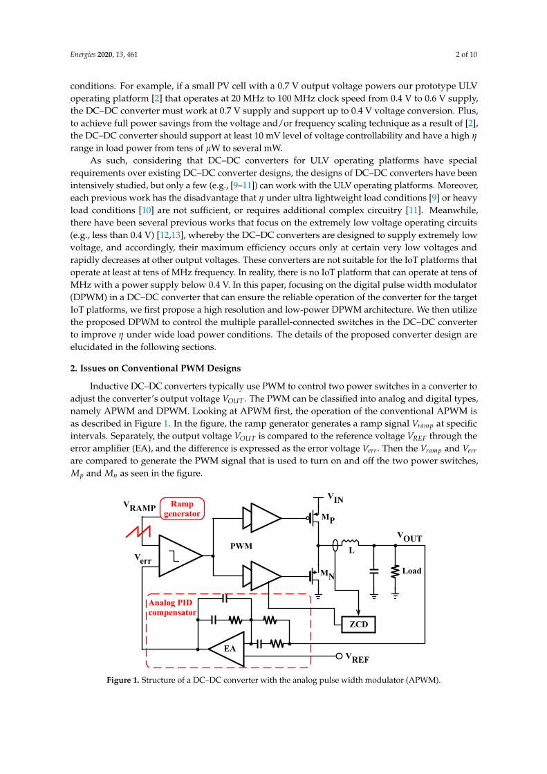
Inductive DC–DC converters typically use PWM to control two power switches in a converter toadjust the converter’s output voltage VOUT . The PWM can be classified into analog and digital types,namely APWM and DPWM. Looking at APWM first, the operation of the conventional APWM isas described in Figure 1. In the figure, the ramp generator generates a ramp signal Vramp at specificintervals. Separately, the output voltage VOUT is compared to the reference voltage VREF through theerror amplifier (EA), and the difference is expressed as the error voltage Verr. Then the Vramp and Verr
are compared to generate the PWM signal that is used to turn on and off the two power switches,Mp and Mn as seen in the figure.
Ramp generator
Verr
VREF EA
VINVRAMP
PWM
ZCD
L
VOUT
MP
MNLoad
Analog PID compensator
Figure 1. Structure of a DC–DC converter with the analog pulse width modulator (APWM).
Energies 2020, 13, 461 3 of 10
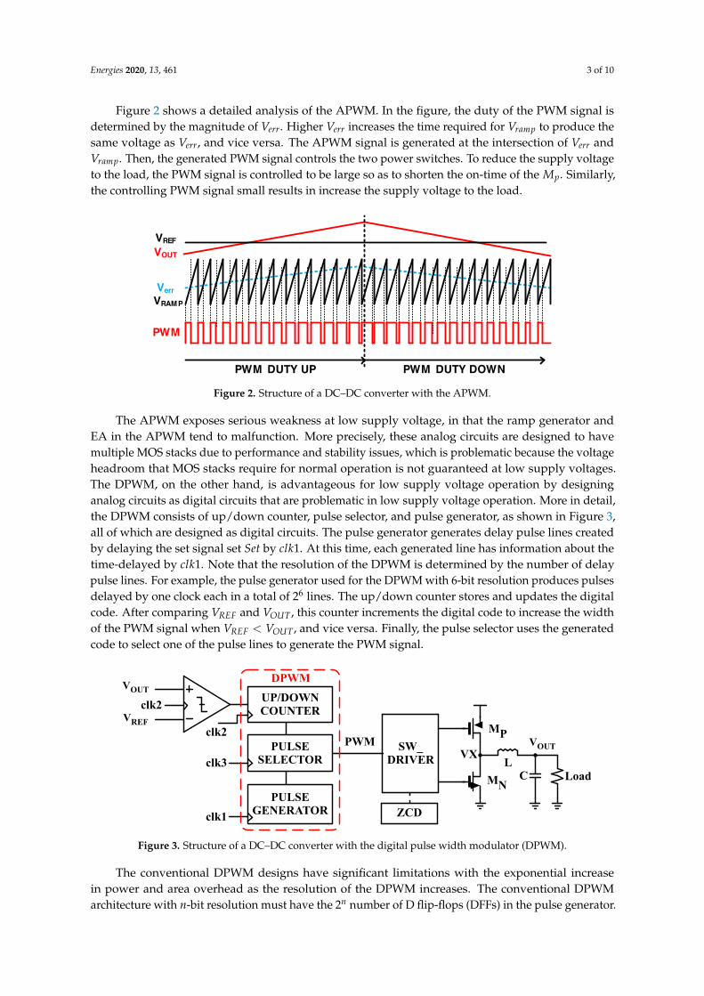
Figure 2 shows a detailed analysis of the APWM. In the figure, the duty of the PWM signal isdetermined by the magnitude of Verr. Higher Verr increases the time required for Vramp to produce thesame voltage as Verr, and vice versa. The APWM signal is generated at the intersection of Verr andVramp. Then, the generated PWM signal controls the two power switches. To reduce the supply voltageto the load, the PWM signal is controlled to be large so as to shorten the on-time of the Mp. Similarly,the controlling PWM signal small results in increase the supply voltage to the load.
VOUT
VREF
VerrVRAMP
PWM
PWM DUTY UP PWM DUTY DOWN
Figure 2. Structure of a DC–DC converter with the APWM.
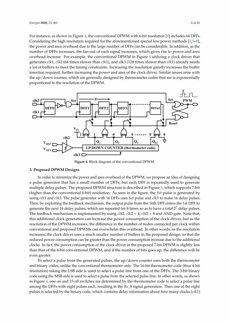
The APWM exposes serious weakness at low supply voltage, in that the ramp generator andEA in the APWM tend to malfunction. More precisely, these analog circuits are designed to havemultiple MOS stacks due to performance and stability issues, which is problematic because the voltageheadroom that MOS stacks require for normal operation is not guaranteed at low supply voltages.The DPWM, on the other hand, is advantageous for low supply voltage operation by designinganalog circuits as digital circuits that are problematic in low supply voltage operation. More in detail,the DPWM consists of up/down counter, pulse selector, and pulse generator, as shown in Figure 3,all of which are designed as digital circuits. The pulse generator generates delay pulse lines createdby delaying the set signal set Set by clk1. At this time, each generated line has information about thetime-delayed by clk1. Note that the resolution of the DPWM is determined by the number of delaypulse lines. For example, the pulse generator used for the DPWM with 6-bit resolution produces pulsesdelayed by one clock each in a total of 26 lines. The up/down counter stores and updates the digitalcode. After comparing VREF and VOUT , this counter increments the digital code to increase the widthof the PWM signal when VREF < VOUT , and vice versa. Finally, the pulse selector uses the generatedcode to select one of the pulse lines to generate the PWM signal.
MN
ZCD
UP/DOWNCOUNTER
PULSEGENERATOR
LoadLC
VXSW_DRIVER
PULSESELECTOR
PWM
clk2
VOUT
VREFclk2
clk3
clk1
MP
DPWM
VOUT
Figure 3. Structure of a DC–DC converter with the digital pulse width modulator (DPWM).
The conventional DPWM designs have significant limitations with the exponential increasein power and area overhead as the resolution of the DPWM increases. The conventional DPWMarchitecture with n-bit resolution must have the 2n number of D flip-flops (DFFs) in the pulse generator.
Energies 2020, 13, 461 4 of 10
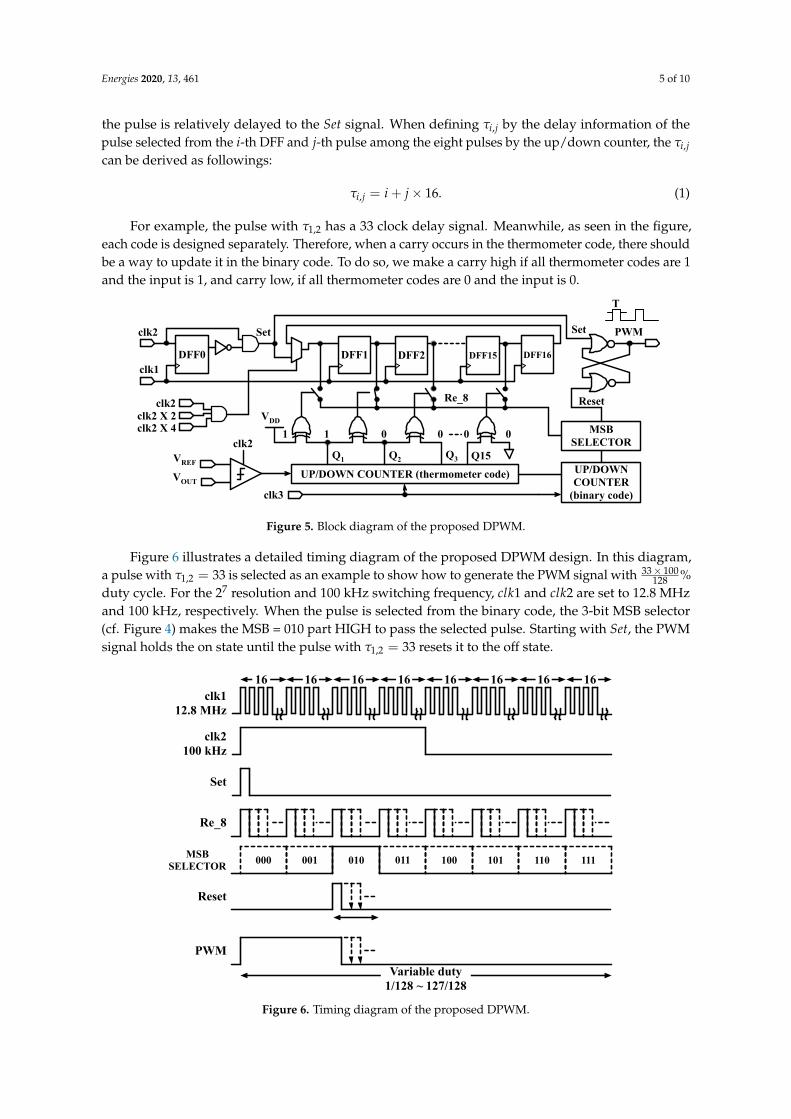
For instance, as shown in Figure 4, the conventional DPWM with 6-bit resolution [9] includes 64 DFFs.Considering the high resolution required for the aforementioned special low power methods [2,5–8],the power and area overhead due to the large number of DFFs can be considerable. In addition, as thenumber of DFFs increases, the fan-out of each signal increases, which gives rise to power and areaoverhead increase. For example, the conventional DPWM in Figure 4 utilizing a clock driver thatgenerates clk1, clk2 (64 times slower than clk1), and clk3 (128 times slower than clk1) already needsa lot of buffers to meet the timing constraints. Increasing the resolution greatly increases the bufferinsertion required, further increasing the power and area of the clock driver. Similar issues arise withthe up/down counter, which are generally designed by thermometer codes that are is exponentiallyproportional to the resolution of the DPWM.
DFF0
clk2
clk1
Set
DFF1 DFF2 DFF3
T
DFF63
Set PWM
T
ResetVIN
Q1 Q2 Q3
1 1 0 0 0 0
Q62
UP/DOWN COUNTER (thermometer code)VREF
VOUT
clk2
clk3
Figure 4. Block diagram of the conventional DPWM.
3. Proposed DPWM Designs
In order to minimize the power and area overhead of the DPWM, we propose an idea of designinga pulse generator that has a small number of DFFs, but each DFF is repeatedly used to generatemultiple delay pulses. The proposed DPWM structure is described in Figure 5, which supports 7-bit(higher than the conventional 6-bit) resolution. As seen in the figure, the Set pulse is generated byusing clk1 and clk2. The pulse generator with 16 DFFs uses Set pulse and clk1 to make 16 delay pulses.Then, by exploiting the feedback mechanism, the output pulse from the 16th DFF enters the 1st DFF togenerate the next 16 delay pulses, which are repeated for 8 times so as to have a total 27 delay pulses.The feedback mechanism is implemented by using clk2, clk2 × 4, clk2 × 8 and AND gate. Note that,this additional clock generation can increase the power consumption of the clock driver, but as theresolution of the DPWM increases, the difference in the number of nodes connected per clock withinconventional and proposed DPWMs can overwhelm this overhead. In other words, as the resolutionincreases, the clock driver uses a much smaller number of buffers in the proposed design, so that thereduced power consumption can be greater than the power consumption increase due to the additionalclocks. In fact, the power consumption of the clock driver in the proposed 7-bit DPWM is slightly lessthan that of the 6-bit conventional DPWM, and if the number of bits goes up, the difference will beeven greater.
To select a pulse from the generated pulses, the up/down counter uses both the thermometerand binary codes, unlike the conventional thermometer only. The 16-bit thermometer code (thus 4-bitresolution) taking the LSB side is used to select a pulse line from one of the DFFs. The 3-bit binarycode using the MSB side is used to select a pulse from the selected pulse line. In other words, as shownin Figure 4, one on and 15 off switches are determined by the thermometer code to select a pulse lineamong the DFFs with eight pulses each, resulting in the Re_8 signal generation. Then one of the eightpulses is selected by the binary code, which contains delay information about how many clocks (clk1)
Energies 2020, 13, 461 5 of 10
the pulse is relatively delayed to the Set signal. When defining τi,j by the delay information of thepulse selected from the i-th DFF and j-th pulse among the eight pulses by the up/down counter, the τi,jcan be derived as followings:
τi,j = i + j × 16. (1)
For example, the pulse with τ1,2 has a 33 clock delay signal. Meanwhile, as seen in the figure,each code is designed separately. Therefore, when a carry occurs in the thermometer code, there shouldbe a way to update it in the binary code. To do so, we make a carry high if all thermometer codes are 1and the input is 1, and carry low, if all thermometer codes are 0 and the input is 0.
DFF0
clk2
clk1
Set
DFF1 DFF2 DFF16
Set
Re_8
VDD
Q1 Q2 Q3
1 1 0 0 0 0
Q15
UP/DOWN COUNTER (thermometer code)VREF
VOUT
clk2
clk3
clk2clk2 X 2
UP/DOWN COUNTER
(binary code)
Reset
MSBSELECTOR
DFF15
clk2 X 4
PWM
T
Figure 5. Block diagram of the proposed DPWM.
Figure 6 illustrates a detailed timing diagram of the proposed DPWM design. In this diagram,a pulse with τ1,2 = 33 is selected as an example to show how to generate the PWM signal with 33× 100
128 %duty cycle. For the 27 resolution and 100 kHz switching frequency, clk1 and clk2 are set to 12.8 MHzand 100 kHz, respectively. When the pulse is selected from the binary code, the 3-bit MSB selector(cf. Figure 4) makes the MSB = 010 part HIGH to pass the selected pulse. Starting with Set, the PWMsignal holds the on state until the pulse with τ1,2 = 33 resets it to the off state.
clk112.8 MHz
clk2100 kHz
Set
Re_8
16
MSBSELECTOR 000 001 010 011 100 101 110 111
16 16 16 16 16 16 16
Reset
PWM
Variable duty 1/128 ~ 127/128
Figure 6. Timing diagram of the proposed DPWM.
Energies 2020, 13, 461 6 of 10
Finally, the proposed DPWM and the conventional DPWM are both fabricated in Samsung 65nm CMOS technology. For the ULV operation, we use the width sizing technique [14,15], so that allthe digital circuits including DFFs, comparator, etc. in the proposed DPWM use the six times largerwidth transistors than the minimum sized transistor in the technology. In case for the conventionalDPWM design, the width of the transistor is sized 24 to 30 times larger than the minimum sizedtransistor of the technology, in order to support a large number of fan-outs. In addition, we adopt thestacking limiting technique [16,17], so that the number of the stacked transistors is limited to four. Themeasured results of the fabricated chip demonstrates that the proposed one achieves significant areareduction and power savings (thereby power conversion efficiency enhancement), compared to theconventional one. The details will be presented in Experimental work.
4. Leverage the Proposed DPWM for Low Power Dynamic Switch Modulation
Dynamic switch width modulation (DSM, or power switch splitting method) is a special techniquefor increasing η under various load power conditions. This technique adaptively turns on or offsome of the multiple parallel-connected switches in a DC–DC converter in response to dynamicallychanging load conditions, maximizing η at a given load power Pload [18–20]. Unfortunately,inevitable area/control overhead caused by the additional logics to detect the load conditions andcontrol the switch selections has limited the efficacy of this technique. Furthermore, this overheadbecomes even more severe when the DC–DC converter powers the ULP platform.
To tackle the overhead problem of the DSM and utilize it to improve η in full load power regionof the ULP platforms, we propose a method that exploits the proposed DPWM design to controlthe power switch selection, instead of using additional detecting logics of the load condition in theconventional DSM. In other words, the proposed DC–DC converter design measures the load conditionusing a digital code originally designed for use in determining the duty cycle of the PWM signal inthe proposed DPWM, which allows the selection of the appropriate switch among several switches.This eliminates the need for load condition detection circuitry for conventional DSMs. For example,the fabricated DC–DC converter targets the ULP platform in [2] is designed to have two different sizesof the power switches (i.e., the width of the big switch and that of the small switch are set to 4:1),and if the PWM duty cycle is less than 3/8, the small switch is selected, otherwise, the large switchis selected. In other words, the digital code 0110000[2] is used as a condition to determine the size ofthe switches. As a result, the minimum conversion efficiency ηmin is higher than 27% @ Pload = 20µW,and the conversion efficiency becomes higher than 60% when Pload ≥ 100µW, and reaches up to themaximum efficiency ηmax = 92.77% @ Pload = 10 mW. Detailed experimental results will be providedin the following section.
5. Experimental Work
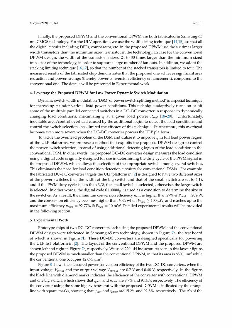
Prototype chips of two DC–DC converters each using the proposed DPWM and the conventionalDPWM design were fabricated in Samsung 65 nm technology, shown in Figure 7a, the test boardof which is shown in Figure 7b. These DC–DC converters are designed specifically for poweringthe ULP IoT platform in [2]. The layout of the conventional DPWM and the proposed DPWM areshown left and right in Figure 7c, respectively. We used 220 µH inductor. As seen in this layout figure,the proposed DPWM is much smaller than the conventional DPWM, in that its area is 8500 µm2 whilethe conventional one occupies 42,075 µm2.
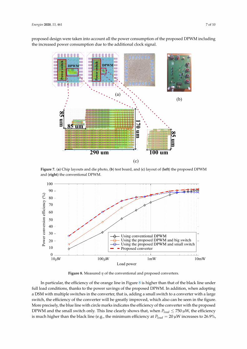
Figure 8 shows the measured power conversion efficiency of the two DC–DC converters, when theinput voltage Vinput and the output voltage Voutput are 0.7 V and 0.48 V, respectively. In the figure,the black line with diamond marks indicates the efficiency of the converter with conventional DPWMand one big switch, which shows that ηmin and ηmax are 8.7% and 91.4%, respectively. The efficiency ofthe converter using the same big switches but with the proposed DPWM is indicated by the orangeline with square marks, showing that ηmin and ηmax are 15.2% and 92.8%, respectively. The η’s of the
Energies 2020, 13, 461 7 of 10
proposed design were taken into account all the power consumption of the proposed DPWM includingthe increased power consumption due to the additional clock signal.
290 um
170 um
85 um
85 um
85 um
100 um(A) (B)(c)
(a)(b)
Pow
er s
witc
h
DPWMPo
wer
sw
itch
DPWM
Figure 7. (a) Chip layouts and die photo, (b) test board, and (c) layout of (left) the proposed DPWMand (right) the conventional DPWM.
10 Wµ<latexit sha1_base64="UxDiKlqS1SSutNz8+sU3Pma6eRA=">AAACxnicjVHLSsNAFD2Nr1pfVZdugkVwFRIRdFlw02VF2wptkSSd1tC8mMwopQj+gFv9NPEP9C+8M05BLaITkpw5954zc+8N8jgqhOu+lqyFxaXllfJqZW19Y3Orur3TLjLJQ9YKszjjV4FfsDhKWUtEImZXOWd+EsSsE4zPVLxzy3gRZemlmOSsn/ijNBpGoS+Iuugl8rpacx1XL3seeAbUYFYzq76ghwEyhJBIwJBCEI7ho6CnCw8ucuL6mBLHCUU6znCPCmklZTHK8Ikd03dEu65hU9orz0KrQzolppeT0sYBaTLK44TVabaOS+2s2N+8p9pT3W1C/8B4JcQK3BD7l26W+V+dqkVgiFNdQ0Q15ZpR1YXGRequqJvbX6oS5JATp/CA4pxwqJWzPttaU+jaVW99HX/TmYpV+9DkSryrW9KAvZ/jnAftI8dzHe/8uFZ3zKjL2MM+DmmeJ6ijgSZa5D3CI57wbDWs1JLW3WeqVTKaXXxb1sMHiB2QQw==</latexit><latexit sha1_base64="UxDiKlqS1SSutNz8+sU3Pma6eRA=">AAACxnicjVHLSsNAFD2Nr1pfVZdugkVwFRIRdFlw02VF2wptkSSd1tC8mMwopQj+gFv9NPEP9C+8M05BLaITkpw5954zc+8N8jgqhOu+lqyFxaXllfJqZW19Y3Orur3TLjLJQ9YKszjjV4FfsDhKWUtEImZXOWd+EsSsE4zPVLxzy3gRZemlmOSsn/ijNBpGoS+Iuugl8rpacx1XL3seeAbUYFYzq76ghwEyhJBIwJBCEI7ho6CnCw8ucuL6mBLHCUU6znCPCmklZTHK8Ikd03dEu65hU9orz0KrQzolppeT0sYBaTLK44TVabaOS+2s2N+8p9pT3W1C/8B4JcQK3BD7l26W+V+dqkVgiFNdQ0Q15ZpR1YXGRequqJvbX6oS5JATp/CA4pxwqJWzPttaU+jaVW99HX/TmYpV+9DkSryrW9KAvZ/jnAftI8dzHe/8uFZ3zKjL2MM+DmmeJ6ijgSZa5D3CI57wbDWs1JLW3WeqVTKaXXxb1sMHiB2QQw==</latexit><latexit sha1_base64="UxDiKlqS1SSutNz8+sU3Pma6eRA=">AAACxnicjVHLSsNAFD2Nr1pfVZdugkVwFRIRdFlw02VF2wptkSSd1tC8mMwopQj+gFv9NPEP9C+8M05BLaITkpw5954zc+8N8jgqhOu+lqyFxaXllfJqZW19Y3Orur3TLjLJQ9YKszjjV4FfsDhKWUtEImZXOWd+EsSsE4zPVLxzy3gRZemlmOSsn/ijNBpGoS+Iuugl8rpacx1XL3seeAbUYFYzq76ghwEyhJBIwJBCEI7ho6CnCw8ucuL6mBLHCUU6znCPCmklZTHK8Ikd03dEu65hU9orz0KrQzolppeT0sYBaTLK44TVabaOS+2s2N+8p9pT3W1C/8B4JcQK3BD7l26W+V+dqkVgiFNdQ0Q15ZpR1YXGRequqJvbX6oS5JATp/CA4pxwqJWzPttaU+jaVW99HX/TmYpV+9DkSryrW9KAvZ/jnAftI8dzHe/8uFZ3zKjL2MM+DmmeJ6ijgSZa5D3CI57wbDWs1JLW3WeqVTKaXXxb1sMHiB2QQw==</latexit><latexit sha1_base64="UxDiKlqS1SSutNz8+sU3Pma6eRA=">AAACxnicjVHLSsNAFD2Nr1pfVZdugkVwFRIRdFlw02VF2wptkSSd1tC8mMwopQj+gFv9NPEP9C+8M05BLaITkpw5954zc+8N8jgqhOu+lqyFxaXllfJqZW19Y3Orur3TLjLJQ9YKszjjV4FfsDhKWUtEImZXOWd+EsSsE4zPVLxzy3gRZemlmOSsn/ijNBpGoS+Iuugl8rpacx1XL3seeAbUYFYzq76ghwEyhJBIwJBCEI7ho6CnCw8ucuL6mBLHCUU6znCPCmklZTHK8Ikd03dEu65hU9orz0KrQzolppeT0sYBaTLK44TVabaOS+2s2N+8p9pT3W1C/8B4JcQK3BD7l26W+V+dqkVgiFNdQ0Q15ZpR1YXGRequqJvbX6oS5JATp/CA4pxwqJWzPttaU+jaVW99HX/TmYpV+9DkSryrW9KAvZ/jnAftI8dzHe/8uFZ3zKjL2MM+DmmeJ6ijgSZa5D3CI57wbDWs1JLW3WeqVTKaXXxb1sMHiB2QQw==</latexit>
100 Wµ<latexit sha1_base64="UxDiKlqS1SSutNz8+sU3Pma6eRA=">AAACxnicjVHLSsNAFD2Nr1pfVZdugkVwFRIRdFlw02VF2wptkSSd1tC8mMwopQj+gFv9NPEP9C+8M05BLaITkpw5954zc+8N8jgqhOu+lqyFxaXllfJqZW19Y3Orur3TLjLJQ9YKszjjV4FfsDhKWUtEImZXOWd+EsSsE4zPVLxzy3gRZemlmOSsn/ijNBpGoS+Iuugl8rpacx1XL3seeAbUYFYzq76ghwEyhJBIwJBCEI7ho6CnCw8ucuL6mBLHCUU6znCPCmklZTHK8Ikd03dEu65hU9orz0KrQzolppeT0sYBaTLK44TVabaOS+2s2N+8p9pT3W1C/8B4JcQK3BD7l26W+V+dqkVgiFNdQ0Q15ZpR1YXGRequqJvbX6oS5JATp/CA4pxwqJWzPttaU+jaVW99HX/TmYpV+9DkSryrW9KAvZ/jnAftI8dzHe/8uFZ3zKjL2MM+DmmeJ6ijgSZa5D3CI57wbDWs1JLW3WeqVTKaXXxb1sMHiB2QQw==</latexit><latexit sha1_base64="UxDiKlqS1SSutNz8+sU3Pma6eRA=">AAACxnicjVHLSsNAFD2Nr1pfVZdugkVwFRIRdFlw02VF2wptkSSd1tC8mMwopQj+gFv9NPEP9C+8M05BLaITkpw5954zc+8N8jgqhOu+lqyFxaXllfJqZW19Y3Orur3TLjLJQ9YKszjjV4FfsDhKWUtEImZXOWd+EsSsE4zPVLxzy3gRZemlmOSsn/ijNBpGoS+Iuugl8rpacx1XL3seeAbUYFYzq76ghwEyhJBIwJBCEI7ho6CnCw8ucuL6mBLHCUU6znCPCmklZTHK8Ikd03dEu65hU9orz0KrQzolppeT0sYBaTLK44TVabaOS+2s2N+8p9pT3W1C/8B4JcQK3BD7l26W+V+dqkVgiFNdQ0Q15ZpR1YXGRequqJvbX6oS5JATp/CA4pxwqJWzPttaU+jaVW99HX/TmYpV+9DkSryrW9KAvZ/jnAftI8dzHe/8uFZ3zKjL2MM+DmmeJ6ijgSZa5D3CI57wbDWs1JLW3WeqVTKaXXxb1sMHiB2QQw==</latexit><latexit sha1_base64="UxDiKlqS1SSutNz8+sU3Pma6eRA=">AAACxnicjVHLSsNAFD2Nr1pfVZdugkVwFRIRdFlw02VF2wptkSSd1tC8mMwopQj+gFv9NPEP9C+8M05BLaITkpw5954zc+8N8jgqhOu+lqyFxaXllfJqZW19Y3Orur3TLjLJQ9YKszjjV4FfsDhKWUtEImZXOWd+EsSsE4zPVLxzy3gRZemlmOSsn/ijNBpGoS+Iuugl8rpacx1XL3seeAbUYFYzq76ghwEyhJBIwJBCEI7ho6CnCw8ucuL6mBLHCUU6znCPCmklZTHK8Ikd03dEu65hU9orz0KrQzolppeT0sYBaTLK44TVabaOS+2s2N+8p9pT3W1C/8B4JcQK3BD7l26W+V+dqkVgiFNdQ0Q15ZpR1YXGRequqJvbX6oS5JATp/CA4pxwqJWzPttaU+jaVW99HX/TmYpV+9DkSryrW9KAvZ/jnAftI8dzHe/8uFZ3zKjL2MM+DmmeJ6ijgSZa5D3CI57wbDWs1JLW3WeqVTKaXXxb1sMHiB2QQw==</latexit><latexit sha1_base64="UxDiKlqS1SSutNz8+sU3Pma6eRA=">AAACxnicjVHLSsNAFD2Nr1pfVZdugkVwFRIRdFlw02VF2wptkSSd1tC8mMwopQj+gFv9NPEP9C+8M05BLaITkpw5954zc+8N8jgqhOu+lqyFxaXllfJqZW19Y3Orur3TLjLJQ9YKszjjV4FfsDhKWUtEImZXOWd+EsSsE4zPVLxzy3gRZemlmOSsn/ijNBpGoS+Iuugl8rpacx1XL3seeAbUYFYzq76ghwEyhJBIwJBCEI7ho6CnCw8ucuL6mBLHCUU6znCPCmklZTHK8Ikd03dEu65hU9orz0KrQzolppeT0sYBaTLK44TVabaOS+2s2N+8p9pT3W1C/8B4JcQK3BD7l26W+V+dqkVgiFNdQ0Q15ZpR1YXGRequqJvbX6oS5JATp/CA4pxwqJWzPttaU+jaVW99HX/TmYpV+9DkSryrW9KAvZ/jnAftI8dzHe/8uFZ3zKjL2MM+DmmeJ6ijgSZa5D3CI57wbDWs1JLW3WeqVTKaXXxb1sMHiB2QQw==</latexit>
1mW 10mWLoad power
Pow
er c
onve
rsio
n ef
ficie
ncy
(%)
10
20
30
40
50
60
70
80
90
100
0
Using conventional DPWM Using the proposed DPWM and big switchUsing the proposed DPWM and small switchProposed converter
Figure 8. Measured η of the conventional and proposed converters.
In particular, the efficiency of the orange line in Figure 8 is higher than that of the black line underfull load conditions, thanks to the power savings of the proposed DPWM. In addition, when adoptinga DSM with multiple switches in the converter, that is, adding a small switch to a converter with a largeswitch, the efficiency of the converter will be greatly improved, which also can be seen in the figure.More precisely, the blue line with circle marks indicates the efficiency of the converter with the proposedDPWM and the small switch only. This line clearly shows that, when Pload ≤ 750µW, the efficiencyis much higher than the black line (e.g., the minimum efficiency at Pload = 20µW increases to 26.9%,
Energies 2020, 13, 461 8 of 10
which can be translated to the 18.2% efficiency improvement.) Finally, without additional circuitry,the DC–DC converter utilizes only digital code (e.g., 0110000[2]) in the proposed DPWM to selectivelycombine orange and blue lines to maximize efficiency under all load conditions. This combined line isshown by the red dotted line in the figure.
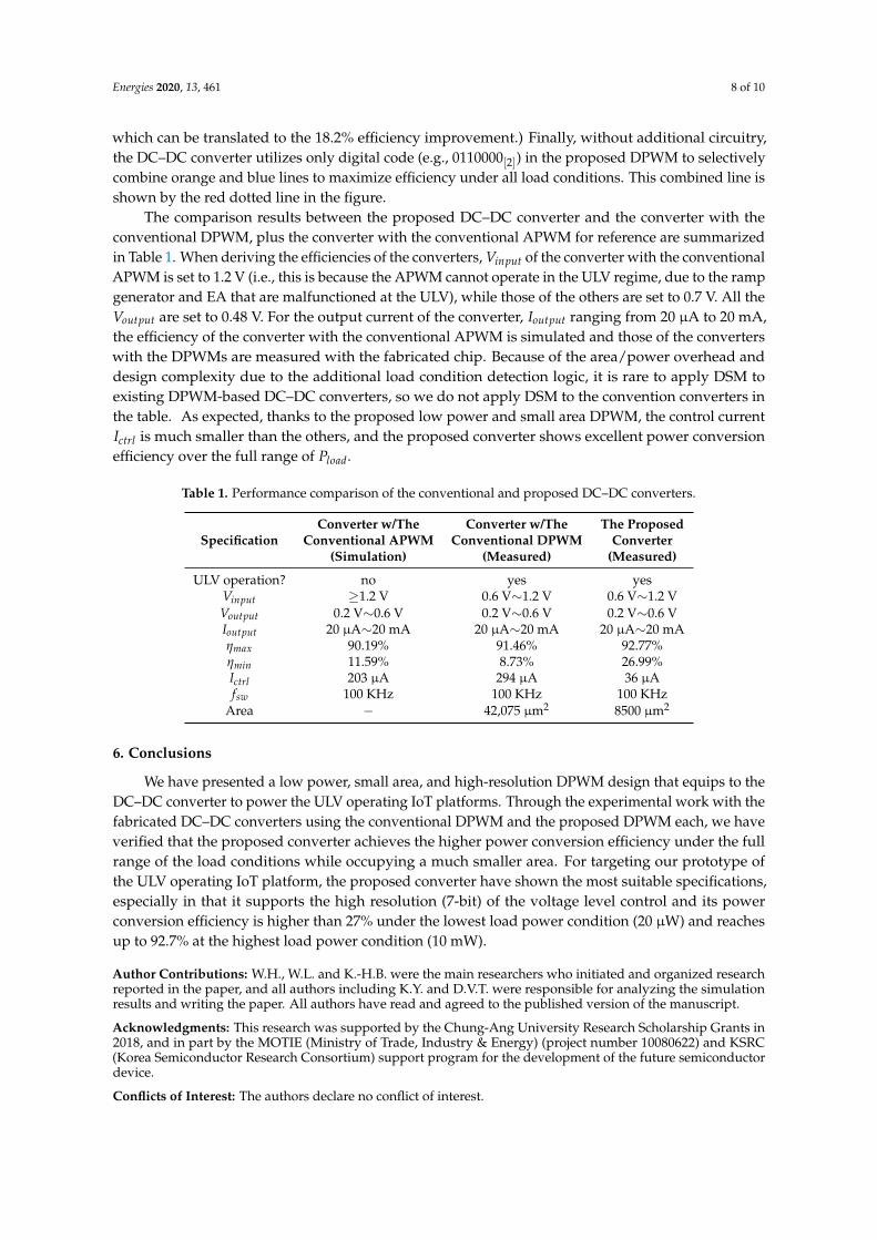
The comparison results between the proposed DC–DC converter and the converter with theconventional DPWM, plus the converter with the conventional APWM for reference are summarizedin Table 1. When deriving the efficiencies of the converters, Vinput of the converter with the conventionalAPWM is set to 1.2 V (i.e., this is because the APWM cannot operate in the ULV regime, due to the rampgenerator and EA that are malfunctioned at the ULV), while those of the others are set to 0.7 V. All theVoutput are set to 0.48 V. For the output current of the converter, Ioutput ranging from 20 µA to 20 mA,the efficiency of the converter with the conventional APWM is simulated and those of the converterswith the DPWMs are measured with the fabricated chip. Because of the area/power overhead anddesign complexity due to the additional load condition detection logic, it is rare to apply DSM toexisting DPWM-based DC–DC converters, so we do not apply DSM to the convention converters inthe table. As expected, thanks to the proposed low power and small area DPWM, the control currentIctrl is much smaller than the others, and the proposed converter shows excellent power conversionefficiency over the full range of Pload.
Table 1. Performance comparison of the conventional and proposed DC–DC converters.
SpecificationConverter w/The Converter w/The The Proposed
Conventional APWM Conventional DPWM Converter(Simulation) (Measured) (Measured)
ULV operation? no yes yesVinput ≥1.2 V 0.6 V∼1.2 V 0.6 V∼1.2 VVoutput 0.2 V∼0.6 V 0.2 V∼0.6 V 0.2 V∼0.6 VIoutput 20 µA∼20 mA 20 µA∼20 mA 20 µA∼20 mAηmax 90.19% 91.46% 92.77%ηmin 11.59% 8.73% 26.99%Ictrl 203 µA 294 µA 36 µAfsw 100 KHz 100 KHz 100 KHz
Area − 42,075 µm2 8500 µm2
6. Conclusions
We have presented a low power, small area, and high-resolution DPWM design that equips to theDC–DC converter to power the ULV operating IoT platforms. Through the experimental work with thefabricated DC–DC converters using the conventional DPWM and the proposed DPWM each, we haveverified that the proposed converter achieves the higher power conversion efficiency under the fullrange of the load conditions while occupying a much smaller area. For targeting our prototype ofthe ULV operating IoT platform, the proposed converter have shown the most suitable specifications,especially in that it supports the high resolution (7-bit) of the voltage level control and its powerconversion efficiency is higher than 27% under the lowest load power condition (20 µW) and reachesup to 92.7% at the highest load power condition (10 mW).
Author Contributions: W.H., W.L. and K.-H.B. were the main researchers who initiated and organized researchreported in the paper, and all authors including K.Y. and D.V.T. were responsible for analyzing the simulationresults and writing the paper. All authors have read and agreed to the published version of the manuscript.
Acknowledgments: This research was supported by the Chung-Ang University Research Scholarship Grants in2018, and in part by the MOTIE (Ministry of Trade, Industry & Energy) (project number 10080622) and KSRC(Korea Semiconductor Research Consortium) support program for the development of the future semiconductordevice.
Conflicts of Interest: The authors declare no conflict of interest.
Energies 2020, 13, 461 9 of 10
References
1. Karnik, T.; Kurian, D.; Aseron, P.; Dorrance, R.; Alpman, E.; Nicoara, A.; Popov, R.; Azarenkov, L.;Moiseev, M.; Zhao, L.; et al. A cm-scale self-powered intelligent and secure IoT edge mote featuringan ultra-low-power SoC in 14nm tri-gate CMOS.In Proceedings of the 2018 IEEE International Solid-StateCircuits Conference-(ISSCC), San Francisco, CA, USA, 11–15 Febuary 2018; pp. 46–48.
2. Han, K.; Lee, S.; Lee, J.J.; Lee, W.; Pedram, M. TIP: A Temperature Effect Inversion-Aware Ultra-Low PowerSystem-on-Chip Platform. In Proceedings of the 2019 IEEE/ACM International Symposium on Low PowerElectronics and Design (ISLPED), Lausanne, Switzerland, 29–31 July 2019; pp. 1–6.
3. NXP. K32W0x MCUs for Wireless IoT Applications. Available online: https://www.nxp.com/docs/en/fact-sheet/K32W0XFS.pdf (accessed on 20 Sepember 2019).
4. Samsung. Bio-Processor. Available online: https://www.samsung.com/semiconductor/products/bio-processor (accessed on 20 Sepember 2019).
5. Lee, W.; Han, K.; Wang, Y.; Cui, T. TEI-power: Temperature effect inversion-aware dynamic thermalmanagement. ACM Trans. Des. Autom. Electron. Syst. 2017, 22, 51:1–51:25. [CrossRef]
6. Rossi, D.; Pullini, A.; Loi, I.; Gautschi, M.; Gurkaynak, F.K.; Teman, A.; Constantin, J.; Burg, A.;Miro-Panades, I.; Beignè, E.; et al. 193 MOPS/mW @ 162 MOPS, 0.32 V to 1.15 V voltage range multi-coreaccelerator for energy efficient parallel and sequential digital processing. In Proceedings of the 2016 IEEESymposium in Low-Power and High-Speed Chips (COOL CHIPS XIX), Yokohama, Japan, 20–22 April 2016;pp. 1–3.
7. Lee, W.; Kang, T.; Lee, J.J.; Han, K.; Kim, J.; Pedram, M. TEI-ULP: Exploiting body biasing to improve theTEI-aware ultra-low power methods. IEEE Trans. Comput.-Aided Des. Integr. Circuits Syst. 2019, 38, 1758–1770.[CrossRef]
8. Han, K.; Lee, J.J.; Lee, J.; Lee, W.; Pedram, M. TEI-NoC: Optimizing Ultra low Power NoCs Exploitingthe Temperature Effect Inversion. IEEE Trans. Comput.-Aided Des. Integr. Circuits Syst. 2018, 37, 458–471.[CrossRef]
9. Zhang, X.; Chen, P.H.; Okuma, Y.; Ishida, K.; Ryu, Y.; Watanabe, K.; Sakurai, T.; Takamiya, M. A 0.6V InputCCM/DCM Operating Digital Buck Converter in 40nm CMOS. IEEE J. Solid-State Circuits 2014, 49, 2377–2386.[CrossRef]
10. Liu, C.W.; Chung, M.J.; Lee, H.H.; Liao, P.C.; Chen, P.H. A single-inductor triple-input-triple-output (SITITO)energy harvesting interface with cycle-by-cycle source tracking and adaptive peak-inductor-current control.In Proceedings of the 2017 IEEE Asian Solid-State Circuits Conference (A-SSCC), Seoul, Korea, 6–8 November2017; pp. 113–116.
11. Chen, P.H.; Cheng, H.C.; Ai, Y.A.; Chung, W.T. Automatic Mode-Selected Energy Harvesting Interface With>80% Power Efficiency Over 200 nW to 10 mW. IEEE Trans. Very Large Scale Integr. (VLSI) Syst. 2018, 26,2898–2906. [CrossRef]
12. Zhang, X.; Pu, Y.; Ishida, K.; Ryu, Y.; Okuma, Y.; Chen, P.H.; Takamiya, M. A 1-V input, 0.2-V to 0.47-Voutput switched-capacitor DC–DC converter with pulse density and width modulation (PDWM) for 57%ripple reduction. In Proceedings of the 2010 IEEE Asian Solid-State Circuits Conference, Beijing, China,8–10 November 2010; pp. 1-4.
13. Turnquist, M.; Hiienkari, M.; Mäkipää, J.; Jevtic, R.; Pohjalainen, E.; Kallio, T.; Koskinen, L. Fully integratedDC–DC converter and a 0.4 V 32-bit CPU with timing-error prevention supplied from a prototype 1.55 VLi-ion battery. In Proceedings of the 2015 Symposium on VLSI Circuits (VLSI Circuits), Kyoto, Japan,17–19 June 2015; pp. C320–C321.
14. Kwong, J.; Ramadass, Y.K.; Verma, N.; Chandrakasan, A.P. A 65nm Sub-Vt Microcontroller with IntegratedSRAM and Switched-Capacitor DC–DC Converter. IEEE J. Solid-State Circuits 2008, 44, 115–126. [CrossRef]
15. Alioto, M. Ultra-Low Power VLSI Circuit Design Demystified and Explained: A Tutorial. IEEE Trans. CircuitsSyst. Regul. Pap. 2012, 59, 3–29. [CrossRef]
16. Zhai, B.; Pant, S.; Nazhandali, L.; Hanson, S.; Olson, J.; Reeves, A.; Blaauw, D. Energy-Efficient SubthresholdProcessor Design. IEEE Trans. Very Large Scale Integr. (VLSI) Syst. 2009, 17, 1127–1137. [CrossRef]
17. Jain, S.; Khare, S.; Yada, S.; Ambili, V.; Salihundam, P.; Ramani, S.; Ramanarayanan, R. A 280mV-to-1.2Vwide-operating-range IA-32 processor in 32nm CMOS. In Proceedings of the 2012 IEEE InternationalSolid-State Circuits Conference, San Francisco, CA, USA, 19–23 Febuary 2012; pp. 66–68.

Energies 2020, 13, 461 10 of 10
18. Kudva, S.S.; Harjani, R. Fully-Integrated On-Chip DC–DC Converter With a 450X Output Range. IEEE J.Solid-State Circuits 2011, 46, 1940–1951. [CrossRef]
19. Lee, W.; Wang, Y.; Shin, D.; Chang, N.; Pedram, M. Optimizing the Power Delivery Network in a SmartphonePlatform. IEEE Trans. Comput.-Aided Des. Integr. Circuits Syst. 2014, 33, 36–49. [CrossRef]
20. Lee, W. Tutorial: Design and Optimization of Power Delivery Network.s IEIE Trans. Smart Processing andComputing 2016, 5, 349–357. [CrossRef]
c© 2020 by the authors. Licensee MDPI, Basel, Switzerland. This article is an open accessarticle distributed under the terms and conditions of the Creative Commons Attribution(CC BY) license (http://creativecommons.org/licenses/by/4.0/).
Copyright © 2022 FDOKUMEN