Parallel-Operation of Discrete SiC BJTs in a 6-kW/250-kHz DC/DC Boost Converter
10
2482 IEEE TRANSACTIONS ON POWER ELECTRONICS, VOL. 29, NO. 5, MAY2014 Parallel-Operation of Discrete SiC BJTs in a 6-kW/250-kHz DC/DC Boost Converter Jacek Rabkowski, Member, IEEE, Dimosthenis Peftitsis, Member, IEEE, and Hans-Peter Nee, Senior Member, IEEE Abstract—This paper describes issues related to parallel connec- tion of SiC bipolar junction transistors (BJTs) in discrete pack- ages. The devices are applied in a high-frequency dc/dc boost converter where the switching losses significantly exceed the con- duction losses. The design and construction of the converter is dis- cussed with special emphasis on successful parallel-operation of the discrete BJTs. All considerations are experimentally illustrated by a 6-kW, 250-kHz boost converter (300 V/600 V). A special solution for the base-drive unit, based on the dual-source driver concept, is also shown in this paper. The performance of this driver and the current sharing of the BJTs are both presented. The power losses and thermal performance of the parallel-connected transis- tors have been determined experimentally for different powers and switching frequencies. An efficiency of 98.23% (±0.02%) was mea- sured using a calorimetric setup, while the maximum temperature difference among the four devices is 12 ◦ C. Index Terms—Bipolar junction transistor (BJT), dc/dc boost converter, parallel-connected switches, silicon carbide (SiC). I. INTRODUCTION M OST types of the available silicon carbide (SiC) power transistors can be found as various designs of unipo- lar devices. The most known examples of such devices are the SiC junction-field-effect transistor (SiC JFET) and the SiC metal-oxide-semiconductor field-effect-transistor (SiC MOS- FET) [1]–[3]. Apart from the unipolar SiC devices, a SiC bipolar junction transistor (SiC BJT) has also been released a few years ago as engineering samples [4]. The features of the SiC BJTs are comparable to the ones of the unipolar devices of the same voltage and current range. Furthermore, the specific on-state re- sistance of the SiC BJTs (down to 2.3 mΩ·cm 2 ) is even lower than for a majority of the currently available SiC field-effect transistors (FETs) [5], [6], while the switching performance is comparable. A drawback of the SiC BJT is the requirement for a continuously supplied base current while the device is kept in the on-state. This significantly increases the power consumption Manuscript received February 4, 2013; revised July 4, 2013; accepted Septem- ber 6, 2013. Date of current version January 10, 2014. Recommended for pub- lication by Associate Editor M. Bakowski. J. Rabkowski is with Institute of Control and Industrial Electronics, Warsaw University of Technology, Koszykowa 75, 00-660 Warsaw, Poland, and also with Laboratory of Electrical Energy Conversion, KTH Royal Institute of Technol- ogy, SE 10044 Stockholm, Sweden (e-mail: [email protected]). D. Peftitsis and H.-P. Nee are with the Laboratory of Electrical Energy Conver- sion (E2C), School of Electrical Engineering, KTH Royal Institute of Technol- ogy, Teknikringen 33, SE-10044 Stockholm, Sweden (e-mail: [email protected]; [email protected]). Color versions of one or more of the figures in this paper are available online at http://ieeexplore.ieee.org. Digital Object Identifier 10.1109/TPEL.2013.2283083 of the base-drive unit compared to the drivers for FETs. On the other hand, the current gain of currently available SiC BJTs is above 50, which makes the use of SiC BJTs more feasible from the base-driver power consumption point-of-view [5]–[7] com- pared to the silicon counterparts of the eighties. In contrast to, for instance the JFET, the bipolar transistor is unable to conduct reverse currents which may count as a drawback in many ap- plications. Thus, an antiparallel diode is necessary for instance when the SiC BJTs operate in an inverter leg. However, in some topologies, such as the dc/dc boost converter, reverse conduc- tion is not required, and hence, the SiC BJT seems to be a good candidate among various power devices for such converters if high efficiency and high switching frequency are both targeted. A 2-kW dc/dc boost converter where a 1200-V/6-A SiC BJT is employed and having an efficiency of approximately 99% at 100 kHz of switching frequency has been presented in [8]. This 2-kW dc/dc boost converter was also compared to a 2-kW boost converter employing a 1200-V SiC JFET. It is found that the efficiency of the BJT converter exceeds the one of the JFET converter assuming approximately equal speeds of the drive units and the same output power [9]. Despite the similar oper- ating conditions of the two converters, the comparison is not entirely fair due to the different chip sizes of the two SiC de- vices. Additional boost converters with SiC BJTs are described in [10] and [11]. Moreover, several successful examples of dc/dc converters where SiC JFETs are employed have already been demonstrated [12]–[18]. In all the cases, however, the limited chip size of the available SiC power devices counts as a crucial problem when higher power ratings are required. The main rea- son for this is probably the low fabrication yields if large chips are fabricated. It is, therefore, clear that the only ways to reach higher current ratings is to either connect discrete SiC devices in parallel or to build SiC modules populated with several SiC chips [19]–[24]. However, there are clear indications that the second solution still suffers from imperfect switching perfor- mance of the module if high switching speeds are desired. In particular, the stray inductances not only of the collector and emitter connections, but also of the base/gate leads, affect the switching performance of the module. At present, therefore, if both high currents and fast switching is desired, the only way to proceed is to parallel-connect several discrete devices [22]. Moreover, in this case, the stray inductances between the legs of the devices might be properly adjusted if they are mounted in an appropriate way in the circuit layout [20]. This paper presents various issues related to parallel connection of discrete SiC BJTs, which are employed in a high-frequency dc/dc boost converter rated at 6 kW and having a 0885-8993 © 2013 IEEE. Personal use is permitted, but republication/redistribution requires IEEE permission. See http://www.ieee.org/publications standards/publications/rights/index.html for more information.
-
Upload
independent -
Category
Documents
-
view
0 -
download
0
Transcript of Parallel-Operation of Discrete SiC BJTs in a 6-kW/250-kHz DC/DC Boost Converter

2482 IEEE TRANSACTIONS ON POWER ELECTRONICS, VOL. 29, NO. 5, MAY 2014
Parallel-Operation of Discrete SiC BJTsin a 6-kW/250-kHz DC/DC Boost Converter
Jacek Rabkowski, Member, IEEE, Dimosthenis Peftitsis, Member, IEEE,and Hans-Peter Nee, Senior Member, IEEE
Abstract—This paper describes issues related to parallel connec-tion of SiC bipolar junction transistors (BJTs) in discrete pack-ages. The devices are applied in a high-frequency dc/dc boostconverter where the switching losses significantly exceed the con-duction losses. The design and construction of the converter is dis-cussed with special emphasis on successful parallel-operation of thediscrete BJTs. All considerations are experimentally illustrated bya 6-kW, 250-kHz boost converter (300 V/600 V). A special solutionfor the base-drive unit, based on the dual-source driver concept,is also shown in this paper. The performance of this driver andthe current sharing of the BJTs are both presented. The powerlosses and thermal performance of the parallel-connected transis-tors have been determined experimentally for different powers andswitching frequencies. An efficiency of 98.23% (±0.02%) was mea-sured using a calorimetric setup, while the maximum temperaturedifference among the four devices is 12 ◦C.
Index Terms—Bipolar junction transistor (BJT), dc/dc boostconverter, parallel-connected switches, silicon carbide (SiC).
I. INTRODUCTION
MOST types of the available silicon carbide (SiC) powertransistors can be found as various designs of unipo-
lar devices. The most known examples of such devices arethe SiC junction-field-effect transistor (SiC JFET) and the SiCmetal-oxide-semiconductor field-effect-transistor (SiC MOS-FET) [1]–[3]. Apart from the unipolar SiC devices, a SiC bipolarjunction transistor (SiC BJT) has also been released a few yearsago as engineering samples [4]. The features of the SiC BJTsare comparable to the ones of the unipolar devices of the samevoltage and current range. Furthermore, the specific on-state re-sistance of the SiC BJTs (down to 2.3 mΩ·cm2 ) is even lowerthan for a majority of the currently available SiC field-effecttransistors (FETs) [5], [6], while the switching performance iscomparable. A drawback of the SiC BJT is the requirement fora continuously supplied base current while the device is kept inthe on-state. This significantly increases the power consumption
Manuscript received February 4, 2013; revised July 4, 2013; accepted Septem-ber 6, 2013. Date of current version January 10, 2014. Recommended for pub-lication by Associate Editor M. Bakowski.
J. Rabkowski is with Institute of Control and Industrial Electronics, WarsawUniversity of Technology, Koszykowa 75, 00-660 Warsaw, Poland, and also withLaboratory of Electrical Energy Conversion, KTH Royal Institute of Technol-ogy, SE 10044 Stockholm, Sweden (e-mail: [email protected]).
D. Peftitsis and H.-P. Nee are with the Laboratory of Electrical Energy Conver-sion (E2C), School of Electrical Engineering, KTH Royal Institute of Technol-ogy, Teknikringen 33, SE-10044 Stockholm, Sweden (e-mail: [email protected];[email protected]).
Color versions of one or more of the figures in this paper are available onlineat http://ieeexplore.ieee.org.
Digital Object Identifier 10.1109/TPEL.2013.2283083
of the base-drive unit compared to the drivers for FETs. On theother hand, the current gain of currently available SiC BJTs isabove 50, which makes the use of SiC BJTs more feasible fromthe base-driver power consumption point-of-view [5]–[7] com-pared to the silicon counterparts of the eighties. In contrast to,for instance the JFET, the bipolar transistor is unable to conductreverse currents which may count as a drawback in many ap-plications. Thus, an antiparallel diode is necessary for instancewhen the SiC BJTs operate in an inverter leg. However, in sometopologies, such as the dc/dc boost converter, reverse conduc-tion is not required, and hence, the SiC BJT seems to be a goodcandidate among various power devices for such converters ifhigh efficiency and high switching frequency are both targeted.A 2-kW dc/dc boost converter where a 1200-V/6-A SiC BJTis employed and having an efficiency of approximately 99%at 100 kHz of switching frequency has been presented in [8].This 2-kW dc/dc boost converter was also compared to a 2-kWboost converter employing a 1200-V SiC JFET. It is found thatthe efficiency of the BJT converter exceeds the one of the JFETconverter assuming approximately equal speeds of the driveunits and the same output power [9]. Despite the similar oper-ating conditions of the two converters, the comparison is notentirely fair due to the different chip sizes of the two SiC de-vices. Additional boost converters with SiC BJTs are describedin [10] and [11]. Moreover, several successful examples of dc/dcconverters where SiC JFETs are employed have already beendemonstrated [12]–[18]. In all the cases, however, the limitedchip size of the available SiC power devices counts as a crucialproblem when higher power ratings are required. The main rea-son for this is probably the low fabrication yields if large chipsare fabricated. It is, therefore, clear that the only ways to reachhigher current ratings is to either connect discrete SiC devicesin parallel or to build SiC modules populated with several SiCchips [19]–[24]. However, there are clear indications that thesecond solution still suffers from imperfect switching perfor-mance of the module if high switching speeds are desired. Inparticular, the stray inductances not only of the collector andemitter connections, but also of the base/gate leads, affect theswitching performance of the module. At present, therefore, ifboth high currents and fast switching is desired, the only wayto proceed is to parallel-connect several discrete devices [22].Moreover, in this case, the stray inductances between the legsof the devices might be properly adjusted if they are mountedin an appropriate way in the circuit layout [20].
This paper presents various issues related to parallelconnection of discrete SiC BJTs, which are employed in ahigh-frequency dc/dc boost converter rated at 6 kW and having a
0885-8993 © 2013 IEEE. Personal use is permitted, but republication/redistribution requires IEEE permission.See http://www.ieee.org/publications standards/publications/rights/index.html for more information.

RABKOWSKI et al.: PARALLEL-OPERATION OF DISCRETE SiC BJTs IN A 6-kW/250-kHz DC/DC BOOST CONVERTER 2483
switching frequency of up to 250 kHz. Four parallel-connected6-A SiC BJTs are employed in order to reach the desired powerlevel. The crucial parameters affecting the feasibility of theparallel-connected SiC BJTs are presented in Section II, whileSection III deals with the design process of the converter pro-totype. Details regarding the design of the base-drive unit arecovered in Section IV. Finally, the experimental results showingboth the electrical and the thermal performance of the systemare given in Section V.
II. PARAMETERS INFLUENCING
PARALLEL-CONNECTION OF BJTS
In the ideal case, the nominal current of n parallel-connectedtransistors is n times higher than the nominal current of each sin-gle device; the dissipated power is equally distributed, while thejunction temperatures are the same. Such a situation is obviouslyimpossible to achieve in a real system, but it should be consid-ered as a target during the design of the system with parallel-connected transistors [25]. In practice three main sources ofunbalances might appear [26]:
1) variations in the transistor parameters;2) different driving conditions for the transistors;3) differences in the main circuit layout.
A. Spread in the Device Parameters
The fabrication process of SiC BJTs may lead to differencesin the static transfer characteristics, the current gain β, and/orin the amount of charge required to turn the BJT ON and OFF.Furthermore, the thermal resistance and capacitance is also ex-pected to vary among the parallel-connected devices. Theseissues are, however, out of the scope of this paper, due to thelimited amount of available BJT samples.
B. Nonidentical Driving
As the SiC BJT is a current-controlled device, it requiresa steady-state base current during the on-state and dynamiccurrent peaks during the turn-on and turn-off processes. Thus,any driver mismatches may affect both the conduction and theswitching processes when the transistors are connected in par-allel [25]. Moreover, the base–emitter voltage, VBE , which isquite important from the base driver point-of-view, has a nega-tive temperature coefficient (approximately −1.2 mV/ ◦C) [6].
Any difference in the steady-state base currents of the parallel-connected BJTs will result in an uneven distribution of thecollector currents and, therefore, a steady-state operating pointwhere the devices have different junction temperatures is antic-ipated. A simple attempt to reduce this problem is to use a basedriver with a common supply voltage and a separate base resis-tor for each individual BJT. Then, the hotter transistor with thelower VBE , will be supplied with a slightly higher base current.On the other hand, the relatively low value of the temperaturecoefficient of VBE is reducing the impact of the difference injunction temperatures on the base currents.
A more crucial problem deals with the dynamic base currentvariations as they significantly affect the switching processes.
The turn-on and turn-off transitions of the SiC BJT are mainlyinfluenced by the amount of charge delivered or released to/fromthe base junction. In the ideal case, the shapes of the base currentpeaks at turn-on or turn-off are expected to be the same in orderfor the parallel-connected BJTs to perform in a similar manner.However, devices having the same parameters and driven withuneven current peaks, will have differences in collector cur-rents and, therefore, in the switching energies. The importanceof the problem is accentuated at high switching frequenciesand, especially, at higher switching speeds. As higher and morerapid base current peaks are required, the parasitic parametersof the base-drive circuit and transistor package also becomesignificant.
C. Power Circuit
Moreover, as shown in [20], the circuit layout (see Fig. 2) isalso a crucial factor which affects the switching performance ofthe parallel-connected devices. The stray inductances betweenthe pin connections of the BJTs and the diode in a dc/dc boostconverter, for instance, might contribute to further transient cur-rent mismatches. Thus, an uneven switching loss distribution isexpected, and the importance of the problem increases as theswitching speed does. As the parasitics are part of every realcircuit, the only possible solution is to design the circuit layoutin such a way that the stray inductances of the switching loopsare well balanced.
III. DESIGN AND CONSTRUCTION OF THE 6-kW BOOST
CONVERTER WITH PARALLEL-CONNECTED BJTS
There are three design directions when SiC power devicesare employed in a power converter: high efficiency, high tem-perature, and/or high frequency. In the presented case, a combi-nation between operation at high switching frequency and highefficiency is considered. The four parallel-connected BJTs witha low-voltage drop should switch very fast in order to facilitatelow switching losses at high switching frequencies such thatthe size and volume of the inductor of the 6-kW dc/dc boostconverter could be minimized. Thus, the goal was to switch at afrequency of 250 kHz with a reasonable total efficiency above98% (including the losses associated with the base driver andpassive components). There is no doubt that the key issue ishow to deal with the parallel-connection of four discrete BJTs,and especially the minimization of dynamic mismatches in thecurrent.
By mounting the parallel-connected devices in a correct wayin the circuit layout, transient current mismatches due to differ-ent stray inductances can be reduced or even eliminated. Thestarting point is to extend the simple circuit schematic (seeFig. 1a) into full circuit schematic taking into account para-sitics related to real converter geometry as it is, for instance,proposed in Fig. 1b. This issue may be also studied with thepartial elements equivalent circuit method [27], [28]. In sim-plified approach applied in this paper, the internal parasitic in-ductances (base, collector, and source electrodes) are assumedto be equal among the transistors and, therefore, omitted onthis schematic as they do not influence the mismatches between

2484 IEEE TRANSACTIONS ON POWER ELECTRONICS, VOL. 29, NO. 5, MAY 2014
Fig. 1. (a) Simplified schematic diagram of the dc/dc boost converter and(b) detailed schematic diagram showing the stray-inductances of the proposedcircuit layout.
Fig. 2. BJTs mounted on the base driver and power board to achieve equalparasitic inductances of the package.
parallel-connected devices. This assumption is correct whenthe way of connecting the transistors to the base driver printedcircuit board (PCB) and power board is the same for everyparallel-connected device (see photograph in Fig. 2). Anotherremarkable observation from Fig. 2 is that the impact of thecommon-emitter inductances may be limited by soldering thePCB of the base driver board (discussed in Section IV) as close tothe devices as possible. Again, those inductances are not shownin Fig. 1(b) as they are expected to be equal when the transistorsare mounted in similar manner. The main concern regardingthe design is to keep the inductances of the interconnectionsbalanced in order to make the switching-loop inductances ofthe transistors similar. The output capacitance COUT which isessential during the switching is distributed into three branchesC1 , C2 , and C3 , each placed between the two transistors (C1 be-tween T1 and T2 ,C2 between T2 and T3 , and C3 between T3and T4 , respectively). This makes the circuit more symmetricalas the parasitic inductances of the emitter circuit (LE 11 to LE 34)can be balanced by keeping the same distances between the tran-sistors and the capacitors [see Fig. 3(b)]. The common-collectorcircuit is more advantageous as only one diode per four transis-tors is considered and full symmetry is impossible. The centralplacement of the diode [Fig. 3(a), diode D is mounted below thepower board] contributes to the circuit symmetry, assuming that
Fig. 3. Placement of the elements: (a) without capacitors and drivers and(b) fully mounted dc/dc converter.
the distances between devices and method of the TO-247 mount-ing were the same. Balancing of the parasitic inductances maylead to similar switching loop inductances for the inner transis-tors T2 and T3 (LC 12 + LE 22 equal to LC 34 + LE 23) as wellas the outer transistors T1 and T4 (LC 1 + LC 12 + LE 2 + LE 11equal to LC 3 + LC 34 + LE 3 + LE 34). In spite of all design ef-forts, the outer transistors (T1 , T4) will always perform in aslightly different way than the inner transistors (T2 , T3) due tothe higher parasitic loop inductance. Moreover, the rechargingcurrent of the parasitic capacitance CL of the main inductor isalso more likely to flow through T2 and T3 .
All in all, the presented design process of the dc/dc boostconverter, where a symmetrical placement of the four parallel-connected BJTs and the SiC Schottky diode has been used in thecircuit layout, is shown in Figs. 2 and 3. Most of the convertervolume (approximately 1.5 dm3 , dimensions of 175 × 100 ×90 mm) is occupied by the heat sink with air-forced coolingand the input inductor L. A special inductor design using a PM74/59 core with Litz wire has been made in order to obtain lowresistive as well as magnetic power losses. Taking into accountthe expected power losses in the input inductor (150 μH/25 A),the maximum switching frequency was chosen to be 250 kHz.
From the electrical parameters point-of-view, the boost con-verter was designed to show the performance of four parallel-connected SiC BJTs. It is, therefore, clear that the ratings of theconverter have been chosen according to the current and voltageratings of the BJTs. Based on the ratings of the BJT devices(1200 V/6 A), the rated power of the converter was chosen tobe 6 kW. This means that assuming an input direct voltage of
RABKOWSKI et al.: PARALLEL-OPERATION OF DISCRETE SiC BJTs IN A 6-kW/250-kHz DC/DC BOOST CONVERTER 2485
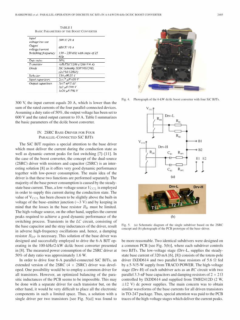
TABLE IBASIC PARAMETERS OF THE BOOST CONVERTER
300 V, the input current equals 20 A, which is lower than thesum of the rated currents of the four parallel-connected devices.Assuming a duty ratio of 50%, the output voltage has been set to600 V and the rated output current to 10 A. Table I summarizesthe basic parameters of the dc/dc boost converter.
IV. 2SRC BASE-DRIVER FOR FOUR
PARALLEL-CONNECTED SiC BJTS
The SiC BJT requires a special attention to the base driverwhich must deliver the current during the conduction state aswell as dynamic current peaks for fast switching [7]–[11]. Inthe case of the boost converter, the concept of the dual-source(2SRC) driver with resistors and capacitor (2SRC) is an inter-esting solution [8] as it offers very good dynamic performancetogether with low-power consumption. The main idea of thedriver is that these two functions are performed separately. Themajority of the base power consumption is caused by the steady-state base current. Thus, a low-voltage source VCCL is employedin order to supply this current during the conduction state. Thevalue of VCCL has been chosen to be slightly above the built-involtage of the base–emitter junction (∼3 V) and by keeping inmind that the losses in the base resistor RB must be limited.The high-voltage source, on the other hand, supplies the currentpeaks required to achieve a good dynamic performance of theswitching process. Transients in the LC circuit, consisting ofthe base capacitor and the stray inductances of the driver, resultin adverse high-frequency oscillations and, hence, a dampingresistor RDP is necessary. This solution of the base driver wasdesigned and successfully employed to drive the 6-A BJT op-erating in the 100-kHz/2-kW dc/dc boost converter presentedin [8]. The measured power consumption of the 2SRC driver at50% of duty ratio was approximately 1.6 W.
In order to drive four 6-A parallel-connected SiC BJTs, anextended version of the 2SRC (4 × 2SRC) driver was devel-oped. One possibility would be to employ a common driver forall transistors. However, an optimized balancing of the para-sitic inductances of the PCB seems to be impossible. This maybe done with a separate driver for each transistor but, on theother hand, it would be very difficult to place all the electroniccomponents in such a limited space. Thus, a solution with asingle driver per two transistors [see Fig. 5(a)] was found to
Fig. 4. Photograph of the 6-kW dc/dc boost converter with four SiC BJTs.
Fig. 5. (a) Schematic diagram of the single subdriver based on the 2SRCconcept and (b) photograph of the PCB prototype of the base–driver.
be more reasonable. Two identical subdrivers were designed ona common PCB [see Fig. 5(b)], where each subdriver controlstwo BJTs. The low-voltage stage (Drv-L, supplies the steady-state base current of 320 mA [6], [8]) consists of the totem-poledriver IXDD614 and two parallel base resistors of 5.6 Ω fedby a 5-V/5-W supply from TRACO POWER. The high-voltagestage (Drv-H) of each subdriver acts as an RC circuit with twoparallel 3.3-nF base capacitors and damping resistors of 2 × 2 Ωcontrolled by IXDD614 and supplied from TMH2412D (2 W,±12 V) dc power supplies. The main concern was to obtainsimilar waveforms of the base currents for all driven transistorsin TO-247 package. Thus, special attention was paid to the PCBtraces of the high-voltage stages which deliver the current peaks.

2486 IEEE TRANSACTIONS ON POWER ELECTRONICS, VOL. 29, NO. 5, MAY 2014
Fig. 6. Base currents of four parallel-connected transistors (all traces 1A/div,time-scale: 100 ns/div).
On the other hand, the dimensions of the TO-247 packages andthe necessary distance between the transistors due to coolingrequirements result in choosing a trace length in the range of15–25 mm. The accompanied parasitic inductances of the tracesare higher than in the case of a single transistor and higher valuesof damping resistors (RDP1 , RDP2) are necessary. Furthermore,it was very hard to ensure exactly the same distances betweenthe high-voltage stages (Drv-H) and all base/emitter connectionpoints in the real design. As a consequence, the parasitic induc-tance of the base loop might be slightly higher for T1 and T3(see Fig. 5b).
V. EXPERIMENTS
A. Base-Driver Performance
The first set of measurements conducted with the completed6-kW/250-kHz dc/dc converter was focused on the performanceof the base driver. Four base currents were measured using Ultra-mini Rogowski coils [29] in order to compare the waveformsand verifying similar driving conditions. Test results for thesingle switching cycle are presented in Fig. 6. Note that thesemeasurements might not be very precise due to the very denseplacement of the devices. Consequently, the Rogowski coilsmight also interact to each other resulting in measurement er-rors. At first sight, all waveforms look to be uniform, while it isonly the base current of T3 which shows a more negative peakat turn-off. All four traces were recorded as data files and plot-ted using MATLAB in order to show the differences betweenthe waveforms. The average current of the four base currentwaveforms was calculated [see Fig. 7(a)], and then the devia-tion of each base current was also computed [see Fig. 7b(b)] asa difference between the given base current and averaged one.A more detailed analysis of the waveforms in Fig. 7 revealsthat the 2SRC base driver provides a positive current peak of2.3 A at turn-on, and a negative peak of 1.5 A at turn-off. Themaximum deviation observed in Fig. 7(b) for T3 is above 0.5 A,but most of the base current deviations are lower than 0.2 A.Especially important is that all base currents perform similarlyin the first nanoseconds of the turn-on or the turn-off processeswhen they have significant impact on the dynamic sharing ofcollector currents.
Fig. 7. (a) Calculated average base current and (b) deviations for all fourtransistors using MATLAB.
An estimation of the base driver power consumption was per-formed based on the equations presented in [8]. It is found thatan amount of 2.1 W per transistor for a switching frequency of250 kHz and a duty ratio of 50% is expected. Due to this expec-tation, an optional air cooling of the drivers is reasonable (seeFigs. 2–5). The measured power consumption of the 4 × 2SRCdriver was 8.5 W at nominal conditions (switching frequency of250 kHz and 50% of duty ratio, including additional fans).
B. Current Sharing During the Switching Process
A closer look at the mounting of the devices shown in Fig. 2reveals that the access to the collector, which is the middle leg ofthe TO-247 package, is advantageous and again the Rogowskicoils are placed close to each other (and might interact witheach other). However, four coils were connected to measure thecurrent sharing among the transistors which is especially inter-esting during the switching transitions. As the maximum recom-mended operation temperature of the applied coils is 70 ◦C [29],the presented results in Fig. 8 were recorded during the firstminutes of operation at full power (6 kW/250 kHz) beforethe transistor cases and the heat sink reached their steady-state

RABKOWSKI et al.: PARALLEL-OPERATION OF DISCRETE SiC BJTs IN A 6-kW/250-kHz DC/DC BOOST CONVERTER 2487
Fig. 8. Collector currents of four parallel-connected transistors during the(a) turn-on and (b) turn-off processes recorded during operation at nominalpower of 6 kW (all traces: 5 A/div, time scale: 20 ns/div).
temperatures. On the other hand, the switching losses of the SiCtransistors are almost independent of the temperature [1]–[3].The observed waveforms in Fig. 8 show a very good sharing ofthe collector currents, especially during the turn-on transition.All currents rise to 5 A in less than 20 ns (what turns the diodeOFF), then, after 25–40 ns the steady state is reached.
All the presented collector current waveforms were recordedas data files and one additional measurement with the collector–emitter voltage was also conducted. Then, the data were syn-chronized and processed in MATLAB in order to compare theperformance of the transistors during the switching processes.Even though the current deviations would be interesting, themost important values are the switching energies as they influ-ence the switching losses. Fig. 9(a) shows the deviation of theswitching energies from the average values: EONAVG = 43μJand EOFFAVG = 19μJ (turn-on energy is higher due to the col-lector current overshoot). The fastest device is T4 [most positivebase current at turn-on—see Fig. 7(b)] and, in consequence, T4dissipates more turn-on energy than the other devices, espe-cially in comparison to the slowest T1 [again good agreementwith the base current waveform in Fig. 7(b)]. The most im-portant time period is the first nanoseconds of the transitionwhen the collector–emitter voltage is still high. In spite of thehigher current overshoot supplied to T3 (observed after approxi-mately 30 ns), the transistor T2 takes more losses as its collector
Fig. 9. Deviations of the switching energies for all four transistors.
Fig. 10. Recorded waveforms of the inductor current and the collector–emittervoltage during operation at nominal conditions (6 kW and 250 kHz) (VCE :200 V/div, iL : 10 A/div, time scale: 2 μs/div).
current rises faster. An opposite performance may be observedduring turn-off. The collector currents of T1 and T3 fall slower[base currents are less negative during the first nanoseconds—see Fig. 7b(b)] and, in result, they dissipate more turn-off energythan T2 and T4 . In addition, the collector current of T3 is moreoscillative which also contributes to higher power losses. Allin all, the total amount of the switching energy varies between67.2 μJ (T3) and 59 μJ (T2).
C. Electrical Measurements
An experimental investigation of the 6-kW dc/dc boost con-verter was performed at the rated output power with a resistiveload and at various switching frequencies. Various electricalquantities were recorded in order to show the performance ofthe converter. The case temperatures of the parallel-connectedSiC BJTs were also measured under different operating condi-tions. Fig. 10 shows an oscilloscope screenshot with the wave-forms of the inductor current and the collector–emitter voltageof the BJT at an output power of 6 kW when the switching fre-quency equals 250 kHz. These two traces show that the converteroperates normally having a duty ratio around 50%. Besides theinductor current ripple (approximately 5 A as expected), current
2488 IEEE TRANSACTIONS ON POWER ELECTRONICS, VOL. 29, NO. 5, MAY 2014
Fig. 11. Screenshot of the power meter recorded during operation at nominalconditions and a switching frequency of 250 kHz (main circuit losses only).
spikes caused by fast changes of the voltage across the inductorare also observed. It must be noted that the inductor current hasbeen measured using a Rogowski coil (CWT1B) and that onlythe ac component is visible.
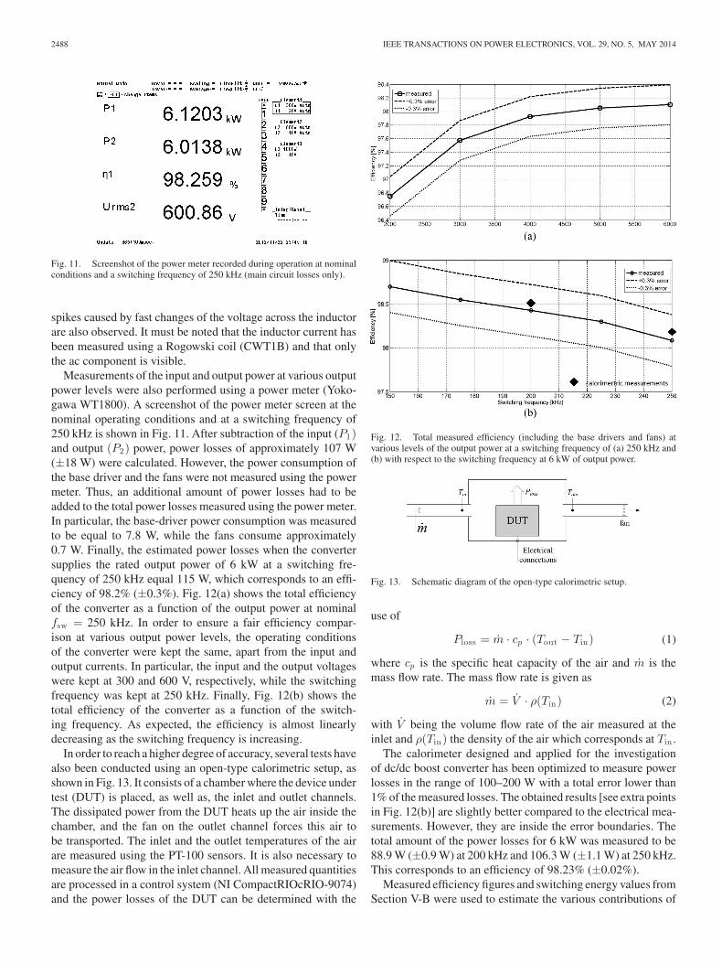
Measurements of the input and output power at various outputpower levels were also performed using a power meter (Yoko-gawa WT1800). A screenshot of the power meter screen at thenominal operating conditions and at a switching frequency of250 kHz is shown in Fig. 11. After subtraction of the input (P1)and output (P2) power, power losses of approximately 107 W(±18 W) were calculated. However, the power consumption ofthe base driver and the fans were not measured using the powermeter. Thus, an additional amount of power losses had to beadded to the total power losses measured using the power meter.In particular, the base-driver power consumption was measuredto be equal to 7.8 W, while the fans consume approximately0.7 W. Finally, the estimated power losses when the convertersupplies the rated output power of 6 kW at a switching fre-quency of 250 kHz equal 115 W, which corresponds to an effi-ciency of 98.2% (±0.3%). Fig. 12(a) shows the total efficiencyof the converter as a function of the output power at nominalfsw = 250 kHz. In order to ensure a fair efficiency compar-ison at various output power levels, the operating conditionsof the converter were kept the same, apart from the input andoutput currents. In particular, the input and the output voltageswere kept at 300 and 600 V, respectively, while the switchingfrequency was kept at 250 kHz. Finally, Fig. 12(b) shows thetotal efficiency of the converter as a function of the switch-ing frequency. As expected, the efficiency is almost linearlydecreasing as the switching frequency is increasing.
In order to reach a higher degree of accuracy, several tests havealso been conducted using an open-type calorimetric setup, asshown in Fig. 13. It consists of a chamber where the device undertest (DUT) is placed, as well as, the inlet and outlet channels.The dissipated power from the DUT heats up the air inside thechamber, and the fan on the outlet channel forces this air tobe transported. The inlet and the outlet temperatures of the airare measured using the PT-100 sensors. It is also necessary tomeasure the air flow in the inlet channel. All measured quantitiesare processed in a control system (NI CompactRIOcRIO-9074)and the power losses of the DUT can be determined with the
Fig. 12. Total measured efficiency (including the base drivers and fans) atvarious levels of the output power at a switching frequency of (a) 250 kHz and(b) with respect to the switching frequency at 6 kW of output power.
Fig. 13. Schematic diagram of the open-type calorimetric setup.
use of
Ploss = m · cp · (Tout − Tin) (1)
where cp is the specific heat capacity of the air and m is themass flow rate. The mass flow rate is given as
m = V · ρ(Tin ) (2)
with V being the volume flow rate of the air measured at theinlet and ρ(Tin ) the density of the air which corresponds at Tin .
The calorimeter designed and applied for the investigationof dc/dc boost converter has been optimized to measure powerlosses in the range of 100–200 W with a total error lower than1% of the measured losses. The obtained results [see extra pointsin Fig. 12(b)] are slightly better compared to the electrical mea-surements. However, they are inside the error boundaries. Thetotal amount of the power losses for 6 kW was measured to be88.9 W (±0.9 W) at 200 kHz and 106.3 W (±1.1 W) at 250 kHz.This corresponds to an efficiency of 98.23% (±0.02%).
Measured efficiency figures and switching energy values fromSection V-B were used to estimate the various contributions of
RABKOWSKI et al.: PARALLEL-OPERATION OF DISCRETE SiC BJTs IN A 6-kW/250-kHz DC/DC BOOST CONVERTER 2489
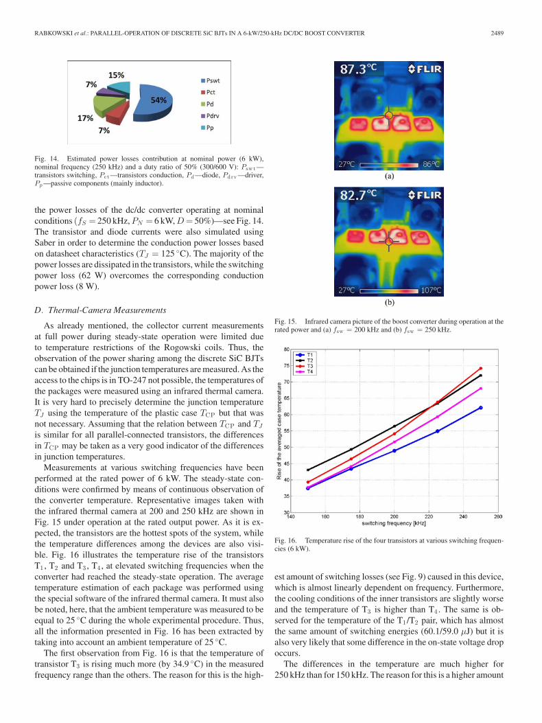
Fig. 14. Estimated power losses contribution at nominal power (6 kW),nominal frequency (250 kHz) and a duty ratio of 50% (300/600 V): Psw t —transistors switching, Pct —transistors conduction, Pd —diode, Pdrv —driver,Pp —passive components (mainly inductor).
the power losses of the dc/dc converter operating at nominalconditions (fS = 250 kHz, PN = 6 kW, D = 50%)—see Fig. 14.The transistor and diode currents were also simulated usingSaber in order to determine the conduction power losses basedon datasheet characteristics (TJ = 125 ◦C). The majority of thepower losses are dissipated in the transistors, while the switchingpower loss (62 W) overcomes the corresponding conductionpower loss (8 W).
D. Thermal-Camera Measurements
As already mentioned, the collector current measurementsat full power during steady-state operation were limited dueto temperature restrictions of the Rogowski coils. Thus, theobservation of the power sharing among the discrete SiC BJTscan be obtained if the junction temperatures are measured. As theaccess to the chips is in TO-247 not possible, the temperatures ofthe packages were measured using an infrared thermal camera.It is very hard to precisely determine the junction temperatureTJ using the temperature of the plastic case TCP but that wasnot necessary. Assuming that the relation between TCP and TJ
is similar for all parallel-connected transistors, the differencesin TCP may be taken as a very good indicator of the differencesin junction temperatures.
Measurements at various switching frequencies have beenperformed at the rated power of 6 kW. The steady-state con-ditions were confirmed by means of continuous observation ofthe converter temperature. Representative images taken withthe infrared thermal camera at 200 and 250 kHz are shown inFig. 15 under operation at the rated output power. As it is ex-pected, the transistors are the hottest spots of the system, whilethe temperature differences among the devices are also visi-ble. Fig. 16 illustrates the temperature rise of the transistorsT1 , T2 and T3 , T4 , at elevated switching frequencies when theconverter had reached the steady-state operation. The averagetemperature estimation of each package was performed usingthe special software of the infrared thermal camera. It must alsobe noted, here, that the ambient temperature was measured to beequal to 25 ◦C during the whole experimental procedure. Thus,all the information presented in Fig. 16 has been extracted bytaking into account an ambient temperature of 25 ◦C.
The first observation from Fig. 16 is that the temperature oftransistor T3 is rising much more (by 34.9 ◦C) in the measuredfrequency range than the others. The reason for this is the high-
Fig. 15. Infrared camera picture of the boost converter during operation at therated power and (a) fsw = 200 kHz and (b) fsw = 250 kHz.
Fig. 16. Temperature rise of the four transistors at various switching frequen-cies (6 kW).
est amount of switching losses (see Fig. 9) caused in this device,which is almost linearly dependent on frequency. Furthermore,the cooling conditions of the inner transistors are slightly worseand the temperature of T3 is higher than T4 . The same is ob-served for the temperature of the T1 /T2 pair, which has almostthe same amount of switching energies (60.1/59.0 μJ) but it isalso very likely that some difference in the on-state voltage dropoccurs.
The differences in the temperature are much higher for250 kHz than for 150 kHz. The reason for this is a higher amount

2490 IEEE TRANSACTIONS ON POWER ELECTRONICS, VOL. 29, NO. 5, MAY 2014
of power losses in total, but also a higher ratio of switchinglosses to conduction losses. It must be noted that the conductionlosses are almost the same regardless the switching frequency.However, the corresponding switching losses are proportionalto the switching frequency. Thus, the power sharing conditionsdiffer as the ratio between the switching losses to conductionlosses is also changing in the measured range of the switchingfrequencies.
Finally, the package temperature differences of the parallel-connected SiC BJTs at steady-state operation under the nom-inal conditions and at a switching frequency of 250 kHz canbe found in Fig. 16. It is clear that the temperature distributionamong the SiC BJTs is not uniform. The temperature differencesindicate that besides the mismatch in the parasitic inductances,there might also be a parameter among the BJTs. The maxi-mum difference appears between the transistor T1 (low switch-ing energy, good cooling conditions) and T3 (highest switchingenergy, slightly worse cooling conditions). In particular, a differ-ence of approximately 12 ◦C was recorded at nominal conditionswhile maximum temperature rise was 74 ◦C (T3). All in all, therecorded temperature differences among the transistors are onan acceptable level and the system of parallel-connected BJTsis operating with a sufficient margin from thermal destruction ofthe hottest transistor (maximum junction temperature of 175 ◦Cis mainly influenced by the TO-247 package).
VI. CONCLUSION
A 6-kW dc/dc boost converter having a nominal switchingfrequency of 250 kHz is presented in this paper. Even thoughthe compact design was not the main goal, the volume of the con-verter is approximately 1.5 dm3 , which means a power densityof 4 kW/L. Four parallel-connected 6-A SiC BJTs are employedas the main switch of the converter and they are driven usinga special version of the dual-source base driver. The driver isdesigned to provide a steady-state base current (320 mA) andhigh current peaks (+2.3/–1.5 A) during turn-on and turn-offtransients of the transistors. The conducted measurements haveshown that the base current waveforms are in a good agree-ment and, besides the turn-off of transistor T3 , the deviationsfrom average value are lower than 0.2 A. Nonsimilarities in thedriving conditions, along with mismatches in the parasitic in-ductances of the power board and, possible differences in thedevice parameters affect the current sharing among the tran-sistors. The parasitic inductances of the switching loops arebalanced by suitable mounting of the transistors and placementof distributed capacitors. However, a fully symmetrical designof the dc/dc boost converter circuit with four transistors andsingle diode is not possible. In result, the amount of measuredswitching energies varies between 59 and 67.2 μJ (12% of vari-ations) and a strong correlation with driving mismatches is vis-ible. Temperature measurements using an infrared camera werealso conducted under operation at full power of the converterand they are in a good agreement with electrical measurements.For instance, the strongest dependence on frequency shows thecase temperature of transistor T3 , which has the highest amountof switching energy. All in all, the package temperature dif-
ferences, which imply junction temperature variations of theBJTs, are on an acceptable level even at nominal conditions.The recorded waveforms show that the transistors are switchingvery fast (tens of nanoseconds) and this fact, in conjunction withthe low on-state voltage drop results in a very high efficiency atthis range of power and switching frequency (250 kHz/6 kW).Last but not least, the high efficiency of the presented dc/dcconverter was verified using a calorimetric measurement setup.The efficiency of the hard-switched dc/dc converter at the ratedconditions was measured to be equal to 98.23% (±0.02%). Themajority of the power losses are caused in the transistors, whilethe power consumption of the base drivers is almost 7.5% of thetotal losses (8.5 W).
REFERENCES
[1] P. Friedrichs, “Silicon carbide power semiconductors—New opportunitiesfor high efficiency,” in Proc. IEEE 3rd Conf. Ind. Electron. Appl., Jun.3–5, 2008, pp. 1770–1774.
[2] N. Kaminski, “State of the art and future of wide band-gap devices,”presented at 13th Eur. Conf. Power Electron. Appl., Barcelona, Spain,2009.
[3] J. Rabkowski, D. Peftitsis, and H. P. Nee, “SiC power transistors—A newera in power electronics is initiated,” IEEE Ind. Electron. Mag., vol. 6,no. 2, pp. 17–26, Jun. 2012.
[4] H.-S. Lee, M. Domeij, C.-M. Zetterling, R. Ghandi, M. Ostling,F. Allerstam, and E. O. Sveinbjornsson, “1200 V 4H-SiC BJTs with acommon emitter current gain of 60 and low on-resistance,” presented atthe Int. Conf. SiC Related Mater., Otsu, Japan, Oct. 2007.
[5] M. Domeij, A Konstantinov, A. Lindgren, C. Zaring, K. Gumaelius, andM. Reimark, “Large Area 1200 V SiC BJTs with β > 100 and ρon <3 mΩcm2 ,” Mat. Sci. Forum, vol. 717–720, pp. 1123–1126, May 2012.
[6] BitSiC1206BB-P1 datasheet, Transic, 2010.[7] Drive circuit and switching, Appl. Note TSC-TR001, Transic, 2010.[8] J. Rabkowski, G. Tolstoy, D. Peftitsis, and H.-P. Nee, “Low-loss high–
performance base-drive unit for SiC BJTs,” IEEE Trans. Power Electron.,vol. 27, no. 5, pp. 2633–2643, May 2012.
[9] D. Peftitsis, J. Rabkowski, G. Tolstoy, and H.-P. Nee, “Experimental com-parison of dc/dc boost converters with SiC JFETs and SiC bipolar transis-tors,” presented at the 14th Eur. Conf. Power Electron. Appl., Birmingham,U.K., Sep. 2011.
[10] P. Haaf and M. Domeij, “Silicon carbide BJT’s in boost applications,”presented at the PCIM Power Electron. Conf., Nuremberg, Germany,2012.
[11] S. Araujo, L. Menzes, T. Hjort, and P. Zacharias, “The renaissance of theBJT as a highly efficient power device based on SiC material,” presentedat the PCIM Power Electron. Conf., Nuremberg, Germany, 2012.
[12] S. K. Mazumder and P. Jedraszczak, “Evaluation of a SiC dc/dc converterfor plug-in hybrid-electric-vehicle at high inlet-coolant temperature,” IETPower Electron., vol. 4, no. 6, pp. 708–714, Jul. 2011.
[13] E. Cilio, G. Mitchell, M. Schupbach, and A. Lostetter, “SiC intelligentmulti module DC/DC converter system for space applications,” in Proc.IEEE Aerospace Conf., Mar. 7–14, 2009, pp. 1–19.
[14] A. M. Abou-Alfotouh and A. V. Radun, “Comparison among SiC JFETsat 1 MHz hard-switched DC/DC converter,” presented at the IEEE 31stAnnu. Conf. Ind. Electron. Soc., Raleigh, NC, USA, Nov. 2005.
[15] R. Kelley, M. S. Mazzola, and V. Bondarenko, “A scalable SiC devicefor DC/DC converters in future hybrid electric vehicles,” presented at theIEEE 21st Annu. Appl. Power Electron. Conf. Expo., Dallas, TX, USA,Mar. 2006.
[16] R. Kelley and M. S. Mazzola, “SiC JFET gate driver design for use inDC/DC converters,” presented at the IEEE 21st Annu. Appl. Power Elec-tron. Conf. Expo., Dallas, TX, USA, Mar. 19–23 2006.
[17] J. Wang, X. Zhou, J. Li, T. Zhao, A. Q. Huang, R. Callanan, F. Husna, andA. Agarwal, “10-kV SiC MOSFET-based boost converter,” IEEE Trans.Ind. Appl., vol. 45, no. 6, pp. 2056–2063, Nov./Dec. 2009.
[18] A. M. Abou-Alfotouh, A. V. Radun, H.-R. Chang, and C. Winterhalter, “A1 MHz hard-switched silicon carbide DC/DC converter,” in Proc. IEEE18th Annu. Appl. Power Electron. Conf. Expo., Feb. 9–13, 2003, vol. 1,pp. 132–138.

RABKOWSKI et al.: PARALLEL-OPERATION OF DISCRETE SiC BJTs IN A 6-kW/250-kHz DC/DC BOOST CONVERTER 2491
[19] M. Chinthavali, P. Ning, Y. Cui, and L. Tolbert, “Investigation on theparallel operation of discrete SiC BJTs and JFET,” in Proc. IEEE 26thAnnu. Appl. Power Electron. Conf., 2011, pp. 1076–1083.
[20] D. Peftitsis, R. Baburske, J. Rabkowski, J. Lutz, G. Tolstoy, and H-P. Nee,“Challenges regarding parallel-connection of SiC JFETs,” IEEE Trans.Power Electron., vol. 28, no. 3, pp. 1449–1463, Mar. 2013.
[21] F. Xu, D. Jiang, J. Wang, F. Wang, L. M. Tolbert, T. J. Han, and S. J. Kim,“Characterization of a high temperature multichip SiC JFET-based mod-ule,” in Proc. IEEE Energy Convers. Congr. Expo., Sep. 17–22, 2011,pp. 2405–2412.
[22] F. Xu, D. Jiang, J. Wang, F. Wang, L. M. Tolbert, T. J. Han, J. Nagashima,and S. J. Kim, “High temperature packaging of 50 kW three-phase SiCpower module,” in Proc. IEEE 8th Int. Conf. on Power Electron. ECCEAsia, Jun. 2011, pp. 2427–2433.
[23] P. Ning, T. G. Lei, F. Wang, G.-Q. Lu, K. D. T. Ngo, and K. Rajashekara,“A novel high-temperature planar package for Sic multichip phase-legpower module,” IEEE Trans. Power Electron., vol. 25, no. 8, pp. 2059–2067, Aug. 2010.
[24] M. Domeij, A. Konstantinov, M. Bast, R. Eisele, L. Wang, andA. Johansson, “1200 V, 3.3 mΩ SiC bipolar junction transistor powermodules,” in Proc. 8th Eur. Conf. Silicon Carbide Related Mat., 2012,pp. 970–973.
[25] J. B. Forsythe, “Paralleling of Power MOSFETs For High Power Output,”App. Rep. [Online]. Available: www.irf.com
[26] M. N. Jovanovic and F. Lee, “Design considerations for paralleling bipolartransistors,” IEEE Trans. Power Electron., vol. PE-2, no. 4, pp. 328–336,Oct. 1987.
[27] S. Forster and A. Lindemann, “Combined optimisation of thermal behaviorand electrical parasitics in power semiconductor components,” in Proc.13th Eur. Power Electron. Conf., 2009, pp. 1–10.
[28] M. Besacier, M. Coyaud, J. L. Schanen, J. Roudet, and B. Rivet, “HybridSi-SiC fast switching cell modeling and characterization including para-sitic environment description by PEEC method,” in Proc. of 33rd Annu.Power Electron. Spec. Conf., 2002, pp. 1753–1757.
[29] CWT Ultra Miniature Specification, (2010). [Online]. Available: www.pemuk.com
Jacek Rabkowski (M’10) received the M.Sc. andPh.D. degrees in electrical engineering from the War-saw University of Technology, Warsaw, Poland, in2000 and 2005, respectively.
In 2005, he joined the Institute of Control and In-dustrial Electronics, Warsaw University of Technol-ogy, as an Assistant Professor. During 2010–2013,he was a Guest Researcher with the Electrical En-ergy Conversion Laboratory, KTH Royal Institute ofTechnology, Stockholm, Sweden. His research inter-ests include novel topologies of power converters and
pulsewidth modulation techniques, particularly drive units and converters withSiC devices.
Dr. Rabkowski serves as a Chairman of the Joint Industrial Electronics So-ciety/Power Electronics Society Chapter of the IEEE Poland Section.
Dimosthenis Peftitsis (S’03–M’13) was born inKavala, Greece, in 1985. He received the Diplomadegree in electrical and computer engineering fromthe Democritus University of Thrace, Xanthi, Greece,in 2008 and the Ph.D. degree from the KTH Royal In-stitute of Technology, Stockholm, Sweden, in 2013.
He is currently with the Department of ElectricalEnergy Conversion, KTH Royal Institute of Technol-ogy. In 2008, he was at ABB Corporate Research,Vasteras, Sweden, for six months, where he was in-volved in working on his diploma thesis. His current
research interests include gate and base driver design for SiC JFETs and BJTs,as well as protection circuits for normally-ONSiC JFETs.
Hans-Peter Nee (S’91–M’96–SM’04) was born inVasteras, Sweden, in 1963. He received the M.Sc.,Licentiate, and Ph.D. degrees in electrical engi-neering from the KTH Royal Institute of Technol-ogy, Stockholm, Sweden, in 1987, 1992, and 1996,respectively.
In 1999, he became a Professor of power elec-tronics at the KTH Royal Institute of Technology,where he is currently the Head of the Electrical En-ergy Conversion Laboratory. His current research in-terests include power electronic converters, semicon-
ductor components, and control aspects of utility applications, such as flexibleac transmission systems and high-voltage dc transmissions, and variable-speeddrives.
Dr. Nee is a Member of the European Power Electronics and Drives As-sociation, involved with the Executive Council and the International ScientificCommittee. He received several awards for his research. He is an AssociateEditor of the IEEE TRANSACTIONS ON POWER ELECTRONICS. He was on theBoard of the IEEE Sweden Section for several years, serving as its Chairmanduring 2002–2003.