MULTI-PORT DC-DC POWER CONVERTER FOR ... - CORE
135
MULTI-PORT DC-DC POWER CONVERTER FOR RENEWABLE ENERGY APPLICATION A Thesis by HUNG-MING CHOU Submitted to the Office of Graduate Studies of Texas A&M University in partial fulfillment of the requirements for the degree of MASTER OF SCIENCE August 2009 Major Subject: Electrical Engineering brought to you by CORE View metadata, citation and similar papers at core.ac.uk provided by Texas A&M University
-
Upload
khangminh22 -
Category
Documents
-
view
1 -
download
0
Transcript of MULTI-PORT DC-DC POWER CONVERTER FOR ... - CORE

MULTI-PORT DC-DC POWER CONVERTER
FOR
RENEWABLE ENERGY APPLICATION
A Thesis
by
HUNG-MING CHOU
Submitted to the Office of Graduate Studies ofTexas A&M University
in partial fulfillment of the requirements for the degree of
MASTER OF SCIENCE
August 2009
Major Subject: Electrical Engineering
brought to you by COREView metadata, citation and similar papers at core.ac.uk
provided by Texas A&M University

MULTI-PORT DC-DC POWER CONVERTER
FOR
RENEWABLE ENERGY APPLICATION
A Thesis
by
HUNG-MING CHOU
Submitted to the Office of Graduate Studies ofTexas A&M University
in partial fulfillment of the requirements for the degree of
MASTER OF SCIENCE
Approved by:
Chair of Committee, Mehrdad EhsaniCommittee Members, Shankar Bhattacharyya
Karen Butler-PurryWon-jong Kim
Head of Department, Costas N. Georghiades
August 2009
Major Subject: Electrical Engineering

iii
ABSTRACT
Multi-port DC-DC Power Converter
for Renewable Energy Application. (August 2009)
Hung-ming Chou, B.S., National Chiao Tung University
Chair of Advisory Committee: Dr. Mehrdad Ehsani
In recent years, there has been lots of emphasis put on the development of renew-
able energy. While considerable improvement on renewable energy has been made,
there are some inherent limitations for these renewable energies. For example, for
solar and wind power, there is an intermittent nature. For the fuel cell, the dynamics
of electro-chemical reaction is quite slow compared to the electric load. This will
not be acceptable for modern electric application, which requires constant voltage of
constant frequency.
This work proposed and evaluated a new power circuit that can deal with the
problem of the intermittent nature and slow response of the renewable energy.
The proposed circuit integrates different renewable energy sources as well as
energy storage. By integrating renewable energy sources with statistical tendency to
compensate each other, the effect of the intermittent nature can be greatly reduced.
This integration will increase the reliability and utilization of the overall system.
Moreover, the integration of energy storage solves the problem of the slow response
of renewable energy. It can provide the extra energy required by load or absorb the
excessive energy provided by the energy sources, greatly improving the dynamics of
overall system.
To better understand the proposed circuit, “Dual Active Bridge” and “Triple
Active Bridge” were reviewed first. The operation principles and the modeling were

iv
presented. Analysis and design of the overall system were discussed. Controller
design and stability issues were investigated. Furthermore, the function of the central
controller was explained. In the end, different simulations were made and discussed.
Results from the simulations showed that the proposed multi-port DC-DC power
converter had satisfactory performance under different scenarios encountered in prac-
tical renewable energy application. The proposed circuit is an effective solution to the
problem due to the intermittent nature and slow response of the renewable energy.

v
To my beloved family

vi
ACKNOWLEDGMENTS
I would like to express my sincerest appreciation to Dr. M. Ehsani for his inspir-
ing guidance, constant encouragement, and stimulating suggestions throughout the
course of my graduate studies. I also deeply appreciate the members of my commit-
tee, Dr. Shankar Bhattacharyya, Dr. Karen L. Butler-Purry, and Dr. Won-jong Kim
for their valuable comments and interest in this project. My thanks are extended
to the past and present lab members at Texas A&M University: Alex Skorcz, Hugo
E. Mena, Billy Yancey, Guadalupe Gonzalez, Ronald Y. Barazarte, Ali Eskandari,
Sriram Emani, and Richard Smith.
Without my family’s sacrifice and support, this work would not have been pos-
sible. I would like to affirm my indebtedness to my parents, my younger sister, and
my girl friend for their unconditional love, care, support, and encouragement.

vii
TABLE OF CONTENTS
CHAPTER Page
I INTRODUCTION . . . . . . . . . . . . . . . . . . . . . . . . . . 1
A. Introduction . . . . . . . . . . . . . . . . . . . . . . . . . . 1
B. The Importance of Energy Storage . . . . . . . . . . . . . 4
1. For Wind Power . . . . . . . . . . . . . . . . . . . . . 4
2. For Solar Photovoltaics . . . . . . . . . . . . . . . . . 6
3. For Fuel Cell . . . . . . . . . . . . . . . . . . . . . . . 7
4. On Energy Storage . . . . . . . . . . . . . . . . . . . . 7
C. Concept of Hybrid Distributed Generation System . . . . . 8
D. Benefits of Multi-port Converter . . . . . . . . . . . . . . . 9
E. Previous Research Work . . . . . . . . . . . . . . . . . . . 12
F. Research Objective . . . . . . . . . . . . . . . . . . . . . . 13
G. Thesis Outline . . . . . . . . . . . . . . . . . . . . . . . . . 14
II REVIEW OF DUAL ACTIVE BRIDGE . . . . . . . . . . . . . 15
A. Introduction . . . . . . . . . . . . . . . . . . . . . . . . . . 15
B. Circuit Description . . . . . . . . . . . . . . . . . . . . . . 15
C. Phase Shifting Technique . . . . . . . . . . . . . . . . . . . 18
D. Gyrator Model Analysis . . . . . . . . . . . . . . . . . . . 24
1. Introduction to Gyrator . . . . . . . . . . . . . . . . . 24
2. Modeling DAB by Gyrator . . . . . . . . . . . . . . . 25
E. Design . . . . . . . . . . . . . . . . . . . . . . . . . . . . . 27
F. Control . . . . . . . . . . . . . . . . . . . . . . . . . . . . . 30
G. Simulation . . . . . . . . . . . . . . . . . . . . . . . . . . . 31
H. Conclusion . . . . . . . . . . . . . . . . . . . . . . . . . . . 32
III REVIEW OF TRIPLE ACTIVE BRIDGE . . . . . . . . . . . . 34
A. Introduction . . . . . . . . . . . . . . . . . . . . . . . . . . 34
B. Circuit Description of Triple Active Full Bridge . . . . . . 36
C. Circuit Description of Triple Active Half Bridge . . . . . . 41
D. Comparison of Full-Bridge and Half-Bridge TAB . . . . . . 43
E. Controller Design . . . . . . . . . . . . . . . . . . . . . . . 44
F. Simulation . . . . . . . . . . . . . . . . . . . . . . . . . . . 47
1. Simulation for Full-Bridge TAB . . . . . . . . . . . . . 48

viii
CHAPTER Page
2. Simulation for Half-Bridge TAB . . . . . . . . . . . . 50
G. Conclusion . . . . . . . . . . . . . . . . . . . . . . . . . . . 52
IV PROPOSED MULTI-PORT POWER CONVERTER . . . . . . 53
A. Introduction . . . . . . . . . . . . . . . . . . . . . . . . . . 53
B. Circuit Description . . . . . . . . . . . . . . . . . . . . . . 54
C. Design of Proposed Multi-port Power Converter . . . . . . 56
1. Transformer Turn Ratios . . . . . . . . . . . . . . . . 57
2. Leakage Inductance of Transformer . . . . . . . . . . . 57
3. Output Filter Capacitor . . . . . . . . . . . . . . . . . 58
4. Input Inductor L0, L1 . . . . . . . . . . . . . . . . . . 58
5. DC Bus Capacitor CDC . . . . . . . . . . . . . . . . . 59
6. Energy Storage Capacitor . . . . . . . . . . . . . . . . 60
7. Current and Voltage Rating of Switches . . . . . . . . 60
D. Modeling of Proposed Multi-port Power Converter . . . . . 61
1. Transfer Function of v1 . . . . . . . . . . . . . . . . . 63
2. Transfer Function of P0 . . . . . . . . . . . . . . . . . 67
3. How to Find the Operating Point . . . . . . . . . . . . 68
E. Control of Proposed Multi-port Power Converter . . . . . . 70
1. Controller Design for φ10 and φ20 . . . . . . . . . . . . 71
2. Current Control . . . . . . . . . . . . . . . . . . . . . 74
3. DC Bus Voltage Regulation . . . . . . . . . . . . . . . 75
4. Control Strategy for Different Set of Switches . . . . . 77
5. Benefits of PI Controller . . . . . . . . . . . . . . . . . 79
F. Central Controller . . . . . . . . . . . . . . . . . . . . . . . 81
1. Starting of the Circuit . . . . . . . . . . . . . . . . . . 81
2. Power Management . . . . . . . . . . . . . . . . . . . 87
3. Controller Scheduling . . . . . . . . . . . . . . . . . . 88
G. Stability Analysis . . . . . . . . . . . . . . . . . . . . . . . 89
H. Integration of Current Source . . . . . . . . . . . . . . . . 93
V SIMULATION AND DISCUSSION . . . . . . . . . . . . . . . . 96
A. Starting of the Circuit . . . . . . . . . . . . . . . . . . . . 96
B. Dynamics in Load . . . . . . . . . . . . . . . . . . . . . . . 99
C. Large Dynamics in Load . . . . . . . . . . . . . . . . . . . 101
D. Control of Load Voltage . . . . . . . . . . . . . . . . . . . 105
E. Dynamics in Source . . . . . . . . . . . . . . . . . . . . . . 106
F. Integration of Current Sources . . . . . . . . . . . . . . . . 108

ix
CHAPTER Page
G. Power Management . . . . . . . . . . . . . . . . . . . . . . 108
VI CONCLUSION AND FUTURE WORK . . . . . . . . . . . . . . 110
A. Conclusion . . . . . . . . . . . . . . . . . . . . . . . . . . . 110
B. Future Work . . . . . . . . . . . . . . . . . . . . . . . . . . 111
REFERENCES . . . . . . . . . . . . . . . . . . . . . . . . . . . . . . . . . . . 113
APPENDIX A . . . . . . . . . . . . . . . . . . . . . . . . . . . . . . . . . . . 116
VITA . . . . . . . . . . . . . . . . . . . . . . . . . . . . . . . . . . . . . . . . 120

x
LIST OF TABLES
TABLE Page
I Component values for DAB . . . . . . . . . . . . . . . . . . . . . . . 30
II Component values for full-bridge TAB . . . . . . . . . . . . . . . . . 48
III Component values for half-bridge TAB . . . . . . . . . . . . . . . . . 50
IV Specs of the proposed circuit . . . . . . . . . . . . . . . . . . . . . . 57
V Operation time for different conditions . . . . . . . . . . . . . . . . . 61
VI Voltage rating and current rating of all switches . . . . . . . . . . . . 62
VII The dependence of switches . . . . . . . . . . . . . . . . . . . . . . . 79
VIII The feedback signal for different control variables . . . . . . . . . . . 79
IX Controller scheduling . . . . . . . . . . . . . . . . . . . . . . . . . . . 89
X Sweeping range for variables . . . . . . . . . . . . . . . . . . . . . . . 93

xi
LIST OF FIGURES
FIGURE Page
1 Annual investment in new renewable energy capacity [1] . . . . . . . 1
2 Renewable electricity nameplate capacity(MW) and percent cu-
mulative increase from previous year [2] . . . . . . . . . . . . . . . . 2
3 Price range of renewable electricity by technology [2] . . . . . . . . . 3
4 Characteristics of wind turbines [4] . . . . . . . . . . . . . . . . . . . 5
5 Characteristics of photovoltaic [4] . . . . . . . . . . . . . . . . . . . . 6
6 Characteristics of fuel cell [5] . . . . . . . . . . . . . . . . . . . . . . 7
7 Conventional structure of integrating renewable energy sources . . . . 10
8 Application of multi-port DC-DC power converter . . . . . . . . . . . 11
9 Circuit representation of the DAB . . . . . . . . . . . . . . . . . . . 16
10 Switching signal for the switches in the DAB . . . . . . . . . . . . . 17
11 Equivalent circuit of the DAB . . . . . . . . . . . . . . . . . . . . . . 18
12 Power transfer versus phase shift of DAB . . . . . . . . . . . . . . . . 19
13 3 step phase shifting from φ = 0o to 900 for DAB . . . . . . . . . . . 21
14 Signal waveform of phase changing technique with several phase
difference command (a)phase old and phase new [degree], (b)ONTIME
flag (c)TRANSITION flag (d)SL14 . . . . . . . . . . . . . . . . . . . 22
15 Current waveform with continuously changing phase difference
command (a)phase [degree], (b)Iprime [A], (c)Isecond [A] . . . . . . . . 23
16 Symbolic representation of a gyrator . . . . . . . . . . . . . . . . . . 25
17 Gyrator model of the DAB . . . . . . . . . . . . . . . . . . . . . . . 26

xii
FIGURE Page
18 Current waveform at the primary side of the transformer . . . . . . . 29
19 Feedback control block diagram of DAB . . . . . . . . . . . . . . . . 31
20 Voltage control of DAB (a)Vload [V], (b)φ [degree], (c)Ileakage [A] . . . 32
21 Voltage regulation of DAB (a)Vload [V],(b)Pload [W], (c)φ [degree],
(d)Ileakage [A] . . . . . . . . . . . . . . . . . . . . . . . . . . . . . . . 33
22 System overview of three-port power converter . . . . . . . . . . . . . 35
23 Circuit representation of TAB . . . . . . . . . . . . . . . . . . . . . . 36
24 Primary-referred simplified π-model representation of TAB . . . . . . 38
25 Voltage generated by the three TAB bridge . . . . . . . . . . . . . . 41
26 Triple active half bridge . . . . . . . . . . . . . . . . . . . . . . . . . 42
27 Transfer function for TAB . . . . . . . . . . . . . . . . . . . . . . . . 46
28 System block derived by Hao . . . . . . . . . . . . . . . . . . . . . . 47
29 Simulation of full-bridge TAB (a)Vload [V], (b)Pin [W], (c)Pload [W] . 49
30 Simulation of full-bridge TAB (a)φ10 and φ20 [degree], (b)Ileakage
[A], (c)Iin [A], (d)Iin−avg [A] . . . . . . . . . . . . . . . . . . . . . . . 49
31 Simulation of full-bridge TAB (a)Vload [V], (b)Pin [W], (c)Pload [W] . 51
32 Simulation of full-bridge TAB (a)φ10 and φ20 [degree], (b)Ileakage
[A], (c)Iin [A], (d)VDC [V] . . . . . . . . . . . . . . . . . . . . . . . . 51
33 Proposed multi-port power converter . . . . . . . . . . . . . . . . . . 54
34 Transfer function of the system . . . . . . . . . . . . . . . . . . . . . 68
35 Power flow between 3 ports . . . . . . . . . . . . . . . . . . . . . . . 69
36 Flow chart for finding operating point: Φ10 and Φ20 . . . . . . . . . . 70
37 Transfer function of TAB under normal condition . . . . . . . . . . . 71

xiii
FIGURE Page
38 Simplified transfer function of TAB . . . . . . . . . . . . . . . . . . . 72
39 Design procedure for coupled systems . . . . . . . . . . . . . . . . . . 73
40 Inductor circuit during different time period . . . . . . . . . . . . . . 75
41 Current waveform during the current control [23] . . . . . . . . . . . 75
42 DC regulation circuit . . . . . . . . . . . . . . . . . . . . . . . . . . . 76
43 Block diagram for DC voltage regulation . . . . . . . . . . . . . . . . 77
44 Signals for the feedback system . . . . . . . . . . . . . . . . . . . . . 80
45 Flow chart for starting the circuit . . . . . . . . . . . . . . . . . . . . 84
46 Bidirectional current switch connected on load side . . . . . . . . . . 86
47 Flow chart for starting the circuit with all components relaxed . . . . 87
48 Input power command Pin1 for different conditions . . . . . . . . . . 88
49 Block diagram for controller scheduling . . . . . . . . . . . . . . . . . 90
50 Transfer functions of coupled system . . . . . . . . . . . . . . . . . . 91
51 Simplified transfer function of coupled system . . . . . . . . . . . . . 92
52 The poles of closed loop transfer functions under the sweeping of
variables . . . . . . . . . . . . . . . . . . . . . . . . . . . . . . . . . . 94
53 Modified circuit to integrate current source . . . . . . . . . . . . . . 95
54 Block diagram of Pin1 control for current source . . . . . . . . . . . . 95
55 Starting with some component energized (a)IL0 and IL0−cmd [A],
(b)IL1 and IL1−cmd [A], (c) Vload [V], (d) φ10 and φ20 [degree] . . . . 97
56 Starting with some component energized (a) φ10 and φ20 [degree]
, (b)SP2, (c) SPP2, (d)SC14 . . . . . . . . . . . . . . . . . . . . . . 97
57 Starting with all components relaxed (a)VDC [V], (b) VC [V],
(c)Vload [V], (d)controlSS, (e)controlSC , (f)controlSL . . . . . . . . . 98

xiv
FIGURE Page
58 Starting with all components relaxed (a)Pin0, Pin1 [W], (b)φ10 and
φ20 [degree], (c)Ileakage [A], (d)Isecond [A], (e)Itertiary [A] . . . . . . . . 99
59 Simulation of dynamic load (a) Pload [W], (b) Pin0 and Pin1 [W],
(c) Vload [V] . . . . . . . . . . . . . . . . . . . . . . . . . . . . . . . . 100
60 Simulation of dynamic load (a) VC [V], (b) IL0 and IL1 [A], (c)
Ileakage [A] . . . . . . . . . . . . . . . . . . . . . . . . . . . . . . . . . 100
61 Large increase in load power (a)Vload and VC [V], (b)Pin0 and Pin1
[W], (c)Pload [W] . . . . . . . . . . . . . . . . . . . . . . . . . . . . . 101
62 Large increase in load power (a)φ10 and φ20 [degree], (b)IL0 and
IL1 [A], (c)Ileakage [A] . . . . . . . . . . . . . . . . . . . . . . . . . . 102
63 Large decrease in load power (a)Vload and VC [V], (b)Pin0 and Pin1
[W], (c)Pload [W] . . . . . . . . . . . . . . . . . . . . . . . . . . . . . 102
64 Large decrease in load power (a)φ10 and φ20 [degree], (b)IL0 and
IL1 [A], (c)Ileakage [A] . . . . . . . . . . . . . . . . . . . . . . . . . . 103
65 Large decrease to no load (a)Vload and VC [V], (b)Pin0 and Pin1
[W], (c)Pload [W] . . . . . . . . . . . . . . . . . . . . . . . . . . . . . 104
66 Large decrease to no load (a)φ10 and φ20 [degree], (b)IL0 and IL1
[A], (c)Ileakage [A] . . . . . . . . . . . . . . . . . . . . . . . . . . . . 104
67 Output voltage control (a)Pload [W], (b)Pin0 and Pin1 [W], (c) Vload
[V] . . . . . . . . . . . . . . . . . . . . . . . . . . . . . . . . . . . . 105
68 Output voltage control (a)VC [V],(b)IL0 and IL1 [A], (c)Ileakage [A] . 106
69 Pin0 increases (a)Pin0 [W], (b)Pload and Pin1 [W], (c)Vload [V],
(d)VC [V] . . . . . . . . . . . . . . . . . . . . . . . . . . . . . . . . . 107
70 Pin0 decreases (a)Pin0 [W], (b)Pload and Pin1 [W], (c)Vload [V],
(d)VC [V] . . . . . . . . . . . . . . . . . . . . . . . . . . . . . . . . . 107
71 Different input power from current source (a)Pin1 and Pin1−cmd
[W], (b)Vload [V], (c)Pload and Pin0 [W] . . . . . . . . . . . . . . . . . 108

xv
FIGURE Page
72 Control of Pin1 (a)P load [W], (b)Pin0 and Pin1 [W], (c)Vload [V],
(d)VC [V] . . . . . . . . . . . . . . . . . . . . . . . . . . . . . . . . . 109
73 Waveform of dual active bridge . . . . . . . . . . . . . . . . . . . . . 119

1
CHAPTER I
INTRODUCTION
A. Introduction
Due to the environmental problem, e.g., climate change, and political and eco-
nomical reasons, e.g., less dependence on the foreign energy import, high oil price,
renewable energy has attracted enormous attention. Investment worldwide in renew-
able energy has gone from below $10 billion in 1995 to over $70 billion in 2007 [1],
shown in Fig. 1. Since 2000, renewable electricity installations in the U.S., excluding
hydro power, have nearly doubled, and in 2007 there is 33 GW of installed capacity.
Wind power and solar power are the fastest growing renewable energy sectors. In
Fig. 1. Annual investment in new renewable energy capacity [1]
The journal model is IEEE Transactions on Automatic Control.

2
2007, wind capacity installations grew 45% and solar PV grew 40% from the previous
year [2]. Fig. 2 shows the increase of renewable energy from 2000 to 2007.
Fig. 2. Renewable electricity nameplate capacity(MW) and percent cumulative in-
crease from previous year [2]
As great advance in renewable energy has been made, the price for electricity
produced with renewable energy drops. The national average electricity price is about
10 cents per kWh. From Fig. 3, the price for certain kinds of renewable energy is lower
than 10 cents per kWh [2]. As the cost of conventional energy resources is increasing
every year, the receding trend in the cost of renewable technologies is encouraging,
making renewable energy an economical means of power generation in the near future.
Renewable energy technologies not only can solve the climate change and reduce
the dependence on foreign energy import, it is also suitable for distributed power
generation. In remote areas, where there are no transmission lines or the cost of
building new transmission lines is high, renewable energy can provide power without
expensive and complicated grid infrastructure. Distributed power generation system

3
Fig. 3. Price range of renewable electricity by technology [2]
has several advantages [3].
• It can reduce or avoid the necessity to build new transmission/distribution lines
or upgrade existing ones.
• It can be configured to meet peak power needs.
• It can diversify the energy sources and increase the reliability of the grid net-
work.
• It can be configured to provide premium power, when coupled with uninter-
ruptible power supply (UPS).
• It can be located close to the user and can be installed in small increments to
match the load requirement of the customer.

4
B. The Importance of Energy Storage
In spite of the advances made in renewable energy, there are some inherent
problems. One is the intermittent nature. The output power from renewable energy
sources is not constant. Another problem is slow response compared with electric
load. Electric loads may change their power demand in very short time. However, it
takes much longer time to change the output power from renewable energy sources.
A unique feature of renewable energy application is that renewable energy sources
are operated in their optimal operating points. Since the cost of implementing renew-
able energy sources is high, it is desirable to get as much power as possible from the
renewable energy sources. Maximum power points is tracked during the operation.
Therefore, the power output from these sources tends to be constant, no matter how
much the load power is. This concept is like hybrid vehicles. The engine, which pro-
vides power to a electric motor, is operated at its optimal operating point, no matter
how much power the electric motor requires. The difference between the power com-
ing from the engine and the power required by the motor is compensated by energy
storage.
The following subsections will describe several examples and show the importance
of energy storage in renewable energy applications.
1. For Wind Power
Fig. 4 shows the characteristics of wind turbines for different wind speeds (v)
[4]. The X-axis is the rotor speed of the wind turbine, while the Y-axis is the power
extracted by the wind turbine. It can be seen that for a given wind speed, there is
one operating point, where the power output is maximum. For example, if the wind
speed is v1, the rotor speed of the wind turbine is controlled to be ω1 so that the power

5
from the wind turbine is maximum. This is the optimal operating point at which the
wind turbine is controlled to operate. This is called maximum power tracking. There
Fig. 4. Characteristics of wind turbines [4]
are two dynamics encountered in the wind power application. Firstly, if the wind
speed is constant, the load power is changed , for example, from 1000 W to 500 W.
Since the wind turbine is producing 1000 W, if there is no energy storage, the rotor
speed had to be reduced such that the output power from the wind turbine is 500
W. However, it may take longer time for the wind turbine to adjust its rotor speed
because of mechanical dynamics. Also if the rotor speed is changed, the operating
point of the wind turbine would not be optimal, wasting the capability of the wind
turbine. However, if there is energy storage installed in this system, the wind turbine
can still produce 1000 W while the load power is 500 W. This extra 500 W will go to
the energy storage. Therefore, with energy storage, the wind turbine can be operated
at its optimal operating point even if the load requires different power.
Another dynamics is that the wind speed changes while the load power is con-
stant. For example, when the wind speed changes from v1 to v2, the power from the
wind turbine increases. If there is energy storage, this extra power will go into the

6
energy storage while the same power is supplied to the load. Therefore, with the
energy storage, the load can be supplied constant power even if the wind speed is not
constant.
2. For Solar Photovoltaics
Fig. 5 shows the characteristics for solar photovoltaics [4]. The X-axis is the
terminal voltage of the photovoltaic cell while the Y-axis is the power output of the
cell. It can be seen that for a given solar irradiance, there is one point, where the
output power is maximum. The power electronics is controlled such that the terminal
voltage of the solar photovoltaic is the voltage where the optimal operating point is.
Just like wind turbine, the dynamics of the load and the photovoltaics require the
Fig. 5. Characteristics of photovoltaic [4]
usage of energy storage if we want to operate the solar photovoltaic in its optimal
operating points. Then energy storage will provide the deficit power and absorb the
excessive power of the system.

7
3. For Fuel Cell
Fig. 6 shows the characteristics for fuel cells [5]. It can be seen that there is a
point where the efficiency is maximum. This is the operating point at which we want
to operate the fuel cell. At this operating point, the output power from the fuel cell
is fixed. If the load power is changed, the energy storage will compensate the power
difference without changing the output power of the fuel cell.
Fig. 6. Characteristics of fuel cell [5]
Because of the electrochemical reaction, the time to change the output power
of the fuel cell is long compared to the dynamics of electric loads. Energy storage
is needed to provide the rest of the load power. The usage of energy storage will
increase the dynamics of overall system.
4. On Energy Storage
There are many different types of energy storage, including battery, super-capacitor,
flywheel, SMES, hydrogen, compressed air, to name a few. In this work, instead of
batteries, super-capacitors are used as energy storage because they have:
• higher power density

8
• linear relationship between its state-of-charge and its terminal voltage
• longer life
• faster response.
However, the price of super-capacitors is expensive. How to reduce the requirement
of energy storage is vital to reduce the cost of the system. One way to reduce the
requirement of energy storage is by integrating different renewable energy sources
that can compensate with each other so that the energy storage does not need to
provide the whole load power for a long time. This concept will be discussed in the
next section.
C. Concept of Hybrid Distributed Generation System
Hybrid distributed generation system (HDGS) has gained attention in recent
years. This system integrates different kinds of renewable energy sources to increase
the overall stability and utilization [6].
A secure supply based on only one renewable energy source requires a substantial
energy storage. The reason is that the renewable energy is not available during some
period of time. For example, the photovoltaic cells produce zero power during the
night or little power during the cloudy day. Wind energy may not be available if
the wind speed is under certain speed, under which the wind turbine can not extract
energy from the wind. If the system has to provide the power to load during the time
when renewable energy source produces little power, the only way is to use the power
from the energy storage.
If two or even more different renewable energy sources are integrated, the storage
capacity requirement would be greatly reduced, since the fluctuations of these two

9
renewable energy sources may have a statistical tendency to compensate each other.
For example, solar power is high during the day, while the wind power is high at
night. Combining these two sources will approximately produce a constant power to
the load during the entire day.
Another example of HDGS is the integration of photovoltaics and fuel cell. Since
the output power of photovoltaics depends on the solar irradiance. Solar irrandiance
varies during the day. In order to have a constant power output, the output power of
fuel cell is adjusted according to the output power of photovoltaics. In this way, the
total power from the photovoltaics and the fuel cell will be the same even though the
solar irradiannce is not constant. Therefore, a combination of photovoltaic and fuel
cell forms a good pair for HDGS application.
D. Benefits of Multi-port Converter
There are two ways to integrate different renewable energy sources and energy
storage. The conventional way is to use a common DC bus. Separated DC-DC power
converters are used to connect different renewable energy sources to the DC bus. Fig.
7 shows the conventional structure.
However, there are several disadvantages for this structure. First, there are more
power electronic devices, resulting in higher cost. For each renewable energy source,
there has to be a DC-DC converter, which connects the renewable energy source to
the DC bus. Also, there are more conversion steps. The power is transformed from
DC to DC, then from DC to AC if the load is AC load. The efficiency is lower because
of more conversion steps. Another problem is related to voltage levels of renewable
energy sources. If the voltage levels for different renewable energy sources are quite
different, and the DC bus voltage is much higher than that of the renewable energy

10
Fig. 7. Conventional structure of integrating renewable energy sources
sources, the DC-DC converters are operated in extreme case, where duty ratio is closed
either to 1 or 0. In this operating point, the efficiency of the DC-DC converter is much
lower than that when operating in normal case. The last issue is about control. In
the conventional structure, the control is separated. The controller only controls the
DC-DC converter without considering the overall system performance. Although this
control is easy, there should be a central controller such that the power management
can be achieved, and the interaction between the renewable energy sources, energy
storage and load can be taken care of.
Another way of integration is by using multi-port power converters. The multi-
port power converter will connect all renewable energy sources and energy storage.
Some ports are bi-directional if they are connected with energy storage, while some
are uni-directional if they are connected with energy source. Fig. 8 shows one of
the applications of the multi-port DC-DC power converter. This converter integrates
fuel cell, photovoltaic cells, energy storage and the load. If the load is AC, an extra

11
inverter is needed to convert the DC power into the AC power.
Fig. 8. Application of multi-port DC-DC power converter
In this multi-port DC-DC power converter, there will be fewer power devices,
which means the cost of the power converter will be lower than that of the conventional
one. Also, the conversion steps are minimized, resulting in higher efficiency. Due
to the presence of the transformer in some circuits, electric isolation is available,
which is important for safety. With the turn ratio of the transformer in certain
topologies, it will be more efficient to integrate different renewable energy sources of
different voltage levels. Finally, there is a central controller. The controller not only
controls the individual switches, but also manages the whole system. For example,
the controller may give the increase power command to the renewable energy source
in order to charge the depleted energy storage. Another example is the controller can
control the switch to perform the ”Maximum Power Point (MPP)” tracking for the
photovoltaic cell such that the output power is maximum at any operating points.
The central controller will enhance the overall performance of the system.

12
E. Previous Research Work
The concept of multi-port DC-DC converter has been discussed in several papers.
Sachin Jain and Vivek Agarwal [6] and A. Di Napoli, et al., [7] connect different
renewable energy sources in parallel across a common DC bus. Another method
to connect different sources is by using series connection [8]. In this work, the AC
voltage produced by the wind turbine is rectified by a uncontrolled rectifier. This DC
voltage is connected in series with the DC voltage of PV generators. The combined DC
voltage is the input to the PWM voltage source inverter to provide power to AC loads.
Another method of integrating sources is by adding the flux in the multi-winding
transformer [9]. In this circuit, there are two current-source input stage circuits,
three-winding coupled transformer and a common output stage. These components
are connected around the transformer. Magnetic flux addition is used to transfer
power to the load.
However, the above topologies are uni-directional and suitable for low power
application. For renewable energy application, the circuit has to be bi-directional
to integrate energy storage. Also the circuit has to be for high power application.
Therefore, there are some literatures proposing other topologies. There topologies
is based on the two-port circuit proposed by Dr. Doncker [10], where the power
transferred is controlled by phase difference of switching signals. This circuit consists
of two sets of full-bridge circuits. Another version uses two sets of half-bridge circuits
[11], where the number of switches is reduced. Based on two-port topologies, a three-
port circuit, consisting of three sets of full-bridge circuits was proposed by M. Michon,
J. L. Duarte, et al. [12]. H. Tao, A. Kotsopoulos et al. improved this circuit by duty
ratio control to increase the soft-switching operation range and designed the controller
to regulate the load voltage and the input power from renewable energy source. The

13
version of half-bridge was proposed by Danwei Liu and Hui Li, where there are three
sets of half-bridge circuits [13]. The concept of the above circuit is quite similar.
The leakage inductance of the transformer is used to transfer power and two phase
differences are used to control the power flowing between the three ports.
However, these literatures didn’t address how to change phase difference properly
to avoid the un- symmetrical current flowing in the leakage inductance, which may
result in the saturation of the inductor. Also, the controller was designed with trial
and error. Some of the models were derived incorrectly for designing the controller.
Moreover, there is no analysis on the stability issue. Moreover, the practical issues,
such as starting of the circuit, influence of dynamic load, the current ripple of renew-
able energy sources, the variation of input power of renewable energy sources, and
large load variance were not addressed in these literatures.
F. Research Objective
In this work, a new kind of multi-port DC-DC power converter will be proposed
in order to integrate different renewable energy sources and energy storage effec-
tively and economically. The proposed circuit will be analyzed, modeled, designed,
controlled, and simulated. Certain issues related to practical application will be dis-
cussed to verify the usefulness of the propose circuit. They will include the stability
of the circuit under different operating points, how to start this circuit without exter-
nal assistance, how to manage the power flow between the source, the load and the
energy storage, how to control to circuit to regulate or control the load voltage while
keeping the input power from the renewable energy sources almost constant under
the influence of the dynamic load, how to maintain a fixed load voltage under the
influence of the variation of input voltage of renewable energy sources, and how to

14
integrate current-source like renewable energy sources.
G. Thesis Outline
In Chapter I, the trend in the renewable energy will be discussed. The need for
the multi-port DC-DC power converter will be explained. Previous research will be
described and the research objective of this work will be presented.
Chapter II will review the dual active bridge (DAB). This circuit is the funda-
mental circuit of the proposed circuit. Some description and analysis will be made
and some simulation and design will be performed on this circuit.
In Chapter III, triple active bridge (TAB) will be described. This circuit is an
extension of DAB, and is the predecessor of the proposed circuit. The fundamental
circuit operation will be describe and analysis will be made. Some simulation of this
circuit will be presented.
In Chapter IV, the proposed circuit will be described. The analysis and design
will be performed. The mathematical model of the circuit will be derived. Based on
the model, with some techniques in control theories, the controller will be designed.
Stability analysis will be performed. The central controller will be designed and some
practical issues will be addressed.
In Chapter V, the simulation will be performed for different scenarios encounter
in the context of renewable energy application. Performance evaluation and discussion
will be made in this chapter.
Chapter VI will conclude the entire work and future work will be described.

15
CHAPTER II
REVIEW OF DUAL ACTIVE BRIDGE
A. Introduction
High-power-density DC-DC converters have been a hot topic recently, especially
in power supply application, hybrid vehicle, hybrid energy storage system and renew-
able energy. In order to have higher power density, the size of the converter has to be
small. One way to achieve it is by operating the converter at higher frequencies, which
will reduce the size of reactive components, transformers and filters. However, when
the switching frequency is high, the switching losses will be high. There are some
ways of switching that will reduce switching losses. One of them is by soft-switching.
Examples of soft-switched dc/dc converters are the parallel output SRC [14], the
pseudo-resonant converter, the resonant pole [15] and quasi-resonant converters[16].
In this work, dual active bridge (DAB) [10], invented by Dr. De Doncker, will be used
as a building block. Therefore, in this chapter, a brief review of the DAB operation
and analysis will be made and the control and simulation will be performed.
B. Circuit Description
The DAB, shown in Fig. 9, is a DC-AC-DC converter which allows energy trans-
fer between the source and the load. The source side and the load side both are
full-bridge circuits, operated at a fixed frequency. Full bridge circuits have the fol-
lowing features: 1)minimal voltage and current stresses in the devices and 2)minimum
VA rating of the transformer. The two full bridges are connected via a high frequency
transformer. The transformer has several functions. It can integrate different voltage
levels with the turn ratio of the transformer. Also, the transformer provides electrical

16
isolation, which may be required by the industry standard. Finally, the leakage in-
ductor of the transformer can be used as an energy transfer element. In every cycle,
a small fraction of energy from the source is stored in this leakage inductor before it
is transfered to the load. The inductance can be added by using external inductors
connected in series with the transformer.
Fig. 9. Circuit representation of the DAB
The switches of the DAB circuit are operated at a constant frequency. The
switching sequence of the switches on the source side is SS1SS4, SS2SS3, SS1SS4 while
the switching sequence on the load side is SL1SL4, SL2SL3, SL1SL4. The switches
are operated at a fixed frequency and with a fixed duty cycle of 50%. These two
switching sequences do not need to be synchronized. As will be explained later,
the phase difference between these two switching sequences is the important control
variable which can be used to control the power transferred between the source side
and the load side. The switching signal for these switches is shown in Fig. 10.
The equation of the power transferred between these two ports was derived in
Appendix A. Equation (2.1) was obtained by averaging the current flowing out of the

17
V_prime
V_secondary
t
t
t
t
t
SS_14
SS_23
SL_14
SL_23
V_in
V_out
Fig. 10. Switching signal for the switches in the DAB
source.
P =VinVout
NωLlk
φ(1 − | φ |π
) (2.1)
where φ is the phase difference between the two ports.
From this equation, it is clear that the equation is like the power equation in
power systems, where the power transferred is related to source voltage Vin, the load
voltage Vout, the inductor Llk and the phase difference. Since the switches on both
sides are switched with 50% duty cycle, the voltage across the primary side and

18
secondary side of the transformer are square waves. These two square waves have
different phases and magnitudes. If we disregard the magnetizing inductance of the
transformer, the transformer can be represented as a leakage inductor connecting
these two ports. The following equivalent circuit is shown in Fig 11. The equivalent
circuit is quite similar to the equivalent circuit in power systems, except that the
voltage in this case is square wave.
Fig. 11. Equivalent circuit of the DAB
If φ is positive, source side will lead the load side. From Equation (2.1), the
power is positive, which means the power is transferred from the source side to the
load side. If φ is negative, the source side will lag the load side. The power will be
negative, which means the power is transferred back to source side from the load side.
From the Fig 12, which plots power versus phase angle, we can see that when
the angle is 90 degrees, the power transferred is maximum.
C. Phase Shifting Technique
The equation (2.1) calculates the power transferred. Since in nominal cases, Vin,
Vout and Llk are constant, the power transferred can be controlled by the variation of

19
−100 −50 0 50 100−1
−0.8
−0.6
−0.4
−0.2
0
0.2
0.4
0.6
0.8
1
Phase
Pow
er (
p.u.
)
Fig. 12. Power transfer versus phase shift of DAB
phase difference φ between the two ports. The higher phase difference, the higher the
power transferred. In typical operation, the output voltage is required to be constant
even though the load changes. In order to regulate the output voltage under different
loads, the phase difference needs to be changed accordingly. A PI controller is used to
generate phase difference command. With this phase difference command, the gating
signals can be generated.
The PI controller continuously generates phase difference command. If there is
no special techniques by which the phase difference is changed, the current in the
leakage inductor of the transformer will be un-symmetric. If this current is large
enough, the transformer will be saturated.

20
Therefore, in order to change the phase difference properly, which is called phase
shifting, some algorithm is needed to make the current of the leakage inductor sym-
metric, even though the phase difference command is continuously changing. This
algorithm was invented by Dr. M. Ehsani, which was described in [17].
The shortest transient switching sequence for phase shifting in the DAB, without
causing the leakage inductor current imbalance, has three-step. If a change of phase
difference φ in time is ∆tφ, the three transient steps of the sequence are:
∆t(3)1 = ∆t1 −
∆tφ
2(2.2)
∆t(3)2 = ∆t1 −
∆tφ
2(2.3)
∆t(3)3 = ∆t1 (2.4)
where ∆t(3)1 ,∆t
(3)2 ,∆t
(3)3 are the first, second and third steps of a three-step sequence
and ∆t1 is the original switching time interval. The change of phase difference ∆tφ
is divided and distributed in two switching sequences. Figure 13 shows an example
where the phase difference φ is changed from 0o to 90o.
In the above example, the phase difference was changed from one value to another
value. However, in the feedback control scheme, the phase difference command φ
is always changing. The output of the PI controller depends on the controller’s
parameters and the difference between the actual value and the reference value. There
are two problems.
First, since the phase difference command φ is always changing, the change in
phase difference command ∆φ exists even when the circuit is undergoing the proce-
dure of the three-step transient switching sequence to change the phase difference.

21
V_prime
V_secondary
I_prime
I_secondar y
I
phase =0 phase =90
t
t
t
t
t
Delta_t_1
Delta_t_2
Delta_t_3
Fig. 13. 3 step phase shifting from φ = 0o to 900 for DAB
Another problem is that even though it is not the right time to change the
phase difference, the change in phase difference command ∆φ still exists. For proper
operation, the three-step transient switching sequence can not begin until the time
is right. In the example shown in Fig. 13, the right time to begin the three-step
transient switching sequence is when the gating signal is changing. The switching
sequence starts when SS14 is turned on. In other words, the right time is when the
voltage across the transformer changes its polarity. If the phase difference is not

22
changed at the right time, it will be hard to maintain the current balance of the
transformer.
To solve these two problems, a specific program was designed. In this program,
”TRANSITION” flag was used to tell the program when the system was undergoing
the three-steps procedure. Another flag was ”On-Time” flag. This flag told the
program when was the right time to start the three-steps phase shifting procedure.
The program is attached in Appendix B.
Fig. 14. Signal waveform of phase changing technique with several phase differ-
ence command (a)phase old and phase new [degree], (b)ONTIME flag
(c)TRANSITION flag (d)SL14
In Fig 14 , there are two phase shiftings: from 45o to 90o and from 90o to 45o. In
the waveforms, phase old is the current phase difference while phase new is the new
phase difference. The correct time to change phase difference is when the ONTIME
flag is equal to one. Only when the ONTIME flag is equal to one will phase old
become phase new. In this case, phase new is changed from 45o to 90o at 20ms.

23
Since the time is not right, the program will wait until the time is right. As soon
as ONTIME flag becomes one, the program undergoes the three-step phase shifting
procedure. During the transition from 45o to 90o, where TRANSITION flag is equal
to one, the phase new is again changed back to 45o. The program will block the
change of phase new since the system is undergoing the transition procedure. The
program waits until the three-step phase shifting procedure is completed. When it
completes the process, and the time is right, the phase old becomes phase new, and
the system undergoes another three-step phase shifting procedure from 90o to 45o.
In Fig 15, it can be seen that the phase changing technique is successful even
though the phase is continuously changing. Note that the current on the primary
side and on the secondary side of the transformer is symmetric.
Fig. 15. Current waveform with continuously changing phase difference command
(a)phase [degree], (b)Iprime [A], (c)Isecond [A]

24
D. Gyrator Model Analysis
There is another way to analyze the DAB. Gyrator theory, discussed in [18], can
be used in analyzing power converters. It is a very powerful tool. If a switching
circuit is a gyrator, it can be easily analyzed and simulated without considering these
switches. Also, the description of the circuit gained from gyrator models is valid both
in the steady state and transient state. In the following, the gyrator will be briefly
described and the DAB will be analyzed by the gyrator theory.
1. Introduction to Gyrator
A gyrator shown in Fig 16 is a realizable network that couples an input port to
an output port via a gyrastatic coefficient. It has no losses and no storage, and it
transforms one-port network into its dual with its gyration conductance. It can be
described by the following equations:
i1 = gv2 (2.5)
i2 = −gv1 (2.6)
where g is called the gyration conductance and has the unit 1Ω
If the input power and output power are calculated, we will find they are the
same:
v1i1 + v2i2 = v1i1 + (1
gi1)(−gv1) = 0 (2.7)
which means there’s no losses and no storage inside the gyrator.
The gyrator converts a network on one port to its dual with respect to the gyrator
conductance on the other port. A voltage source on the input port is converted as a

25
Fig. 16. Symbolic representation of a gyrator
current source on the output port. Capacitors are transformed into inductors. Also,
circuits in series on the one port of gyrator are transformed into circuits in parallel on
the other port. All of these transformations can be performed in opposite directions.
2. Modeling DAB by Gyrator
Using the gyrator transformation mentioned previously, DAB can be represented
with the gyrator model, which is shown in Fig 17. The circuit consists of two full-
bridge circuits and the transformer.
Since
P =VinVout
NωLlk
φ(1 − | φ |π
) (2.8)
The input power should be equal to the output power. Therefore
Pin = VinIin (2.9)
Pout = VoutIout (2.10)
Pin = Pout = P (2.11)

26
The following is obtained:
Iin =Vout
NωLlk
φ(1 − | φ |π
)
= gVout
(2.12)
From Equation 2.12, the input current of DAB is the product of a constant and the
output voltage. Therefore, the DAB is a gyrator, and the gyrator conductance is
g =1
NωLlk
φ(1 − | φ |π
) (2.13)
Fig. 17. Gyrator model of the DAB
As seen in Fig. 17, with the gyrator conductance the gyrator model of DAB
can be obtained. This circuit is reflected to the load side. The voltage source on the
source side is transformed into the current source with gyrator conductance. This
model is valid for the steady state and transient state.
In steady state, the capacitor is an open circuit, and all the current from the

27
source side is flowing into the resistor. The voltage gain will be
Vout
Vin
= gR (2.14)
In addition to gyrator theory, there is another method to calculate the voltage
gain. Since
P =VinVout
NωLlk
φ(1 − | φ |π
) (2.15)
=V 2
out
R(2.16)
Therefore
Vout
Vin
=1
NωLlk
φ(1 − | φ |π
)R = gR (2.17)
which is the same as (2.14).
E. Design
In this DAB, some circuit components need to be designed, including switching
frequency, turn ratio, leakage inductance of the transformer, filter capacitor, and the
voltage rating and current rating of the switches.
First of all, switching frequency fs needs to be selected. 5 kHz is selected in this
work in order to have smaller reactive component size and less switching losses.
If DAB is required to supply 120V AC voltage, an inverter is needed, and the
output voltage of DAB needs to be 135V.
From the power equation 2.1
P =VinVout
NωLlk
φ(1 − | φ |π
)
the turn ratio, leakage inductance, and the phase difference determine the power

28
transferred. Usually, the phase difference is kept around 45o, not near 90o because of
reactive power issue.
As soon as the input voltage, output voltage, switching frequency, and phase dif-
ference are known, the remaining variables are the turn ratio and leakage inductance
of the transformer. Since the smaller the leakage inductance, the large the current
variation flowing in the transformer. Therefore, it is desirable to have larger leakage
inductance. In order to have larger leakage inductance of transformer while main-
taining the same level of power transferred, the turn ratio, as seen from the equation,
has to be small. Therefore, in this design, turn ratio is chosen to be 1.
Based on the required power transferred, the leakage inductance can be deter-
mined according the following equation.
Llk =VinVout
NωPφ(1 − | φ |
π) (2.18)
Moreover, the current rating and the voltage rating of these switches can be
determined. Since the input voltage of DAB is 100V, the voltage rating of the switches
at the input side is 100V. Since the output voltage of DAB is regulated at 135V,
the voltage rating of the switches at the output side is 135V. The current in the
transformer will flow in these switches. Therefore, the current in the transformer is
the current rating of these switches. The magnitude of current will depend on the
phase shift, input voltage, and output voltage. The current is maximum when the
phase difference is 90o. From the Fig.18, the current in the transformer is changing
rapidly from the highest value to the lowest value in half cycle. The magnitude of
the current can be calculated with the following equation:
| Iprime |=1
2
(
−Vin − V ‘out
)
+(
Vin − V ‘out
)
T4
Llk
(2.19)
where T is the switching period= 1fs
and V ‘out is the referred voltage to the primary

29
Va
Vb
VL_lk
I_prime
Vin
Vout’
t
t
t
t
I_second
(if N=1)
T/2 T
T/4 3T/4
I_ripple
V_ripple
T/2
Fig. 18. Current waveform at the primary side of the transformer
side which is Vout
N.
For the filter capacitor size, it can be simplified by three approximations: 1)
the secondary current is like a triangular waveform; 2) all secondary current flows
into the filter capacitor; 3) the direction of secondary current and that of the current
flowing into the capacitor is the same. With the following equation, the size of the

30
filter capacitor can be found.
Q = C ∗ V (2.20)
T
2Iripple = C ∗ Vripple (2.21)
The designed values of all components in this DAB circuit is summarized in Table I.
Table I. Component values for DAB
component value
input voltage 100V
output voltage 135V
output power 250W
nominal phase π4
switching frequency 5000Hz
turn ratio 1
current rating 80A
voltage rating at input 100V
voltage rating at output 135V
leakage inductor 0.0011H
filter capacitor 7e-5F
F. Control
The load voltage is related to the power transferred and the power transferred is
related to the phase difference, which can be described as:

31
Phase- shifting PWM
Dual Active Bridge
PI Controller
Vload*
phase
Vload
Fig. 19. Feedback control block diagram of DAB
P =VinVout
NωLlk
φ(1 − | φ |π
)
P =V 2
load
R
Therefore, the load voltage can be controlled by the phase difference. In this system,
a PI controller is used to regulate the output voltage under the influence of dynamic
load. In addition to regulating the load voltage, the PI controller can also control the
load voltage Vload to be different value, no matter the load resistance is changing or
fixed.
By using trial and error, the coefficient of the PI controller can be found. Fig 19
shows the block diagram of the feedback system.
G. Simulation
This work used PSIM to simulate the proposed circuit. The reason is PSIM can
incorporate C code into its control circuit with DLL block while in Matlab it is hard
to write this kind of program. Moreover, PSIM has higher simulation speed which
reduces the simulation time greatly.
In the first simulation shown in Fig 20, the output voltage is controlled at three
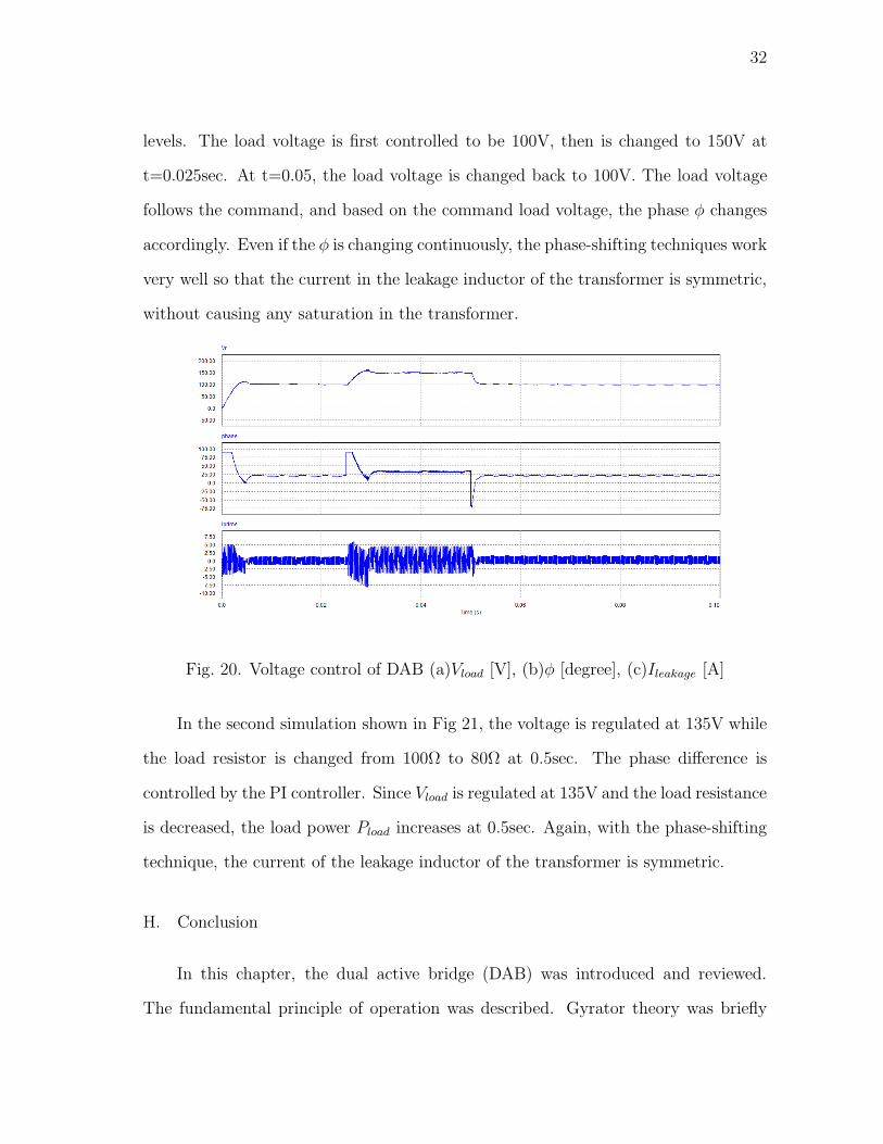
32
levels. The load voltage is first controlled to be 100V, then is changed to 150V at
t=0.025sec. At t=0.05, the load voltage is changed back to 100V. The load voltage
follows the command, and based on the command load voltage, the phase φ changes
accordingly. Even if the φ is changing continuously, the phase-shifting techniques work
very well so that the current in the leakage inductor of the transformer is symmetric,
without causing any saturation in the transformer.
Fig. 20. Voltage control of DAB (a)Vload [V], (b)φ [degree], (c)Ileakage [A]
In the second simulation shown in Fig 21, the voltage is regulated at 135V while
the load resistor is changed from 100Ω to 80Ω at 0.5sec. The phase difference is
controlled by the PI controller. Since Vload is regulated at 135V and the load resistance
is decreased, the load power Pload increases at 0.5sec. Again, with the phase-shifting
technique, the current of the leakage inductor of the transformer is symmetric.
H. Conclusion
In this chapter, the dual active bridge (DAB) was introduced and reviewed.
The fundamental principle of operation was described. Gyrator theory was briefly

33
Fig. 21. Voltage regulation of DAB (a)Vload [V],(b)Pload [W], (c)φ [degree], (d)Ileakage
[A]
introduced and the gyrator model was used to facilitate the analysis of DAB. Also the
component designing was performed according to the desired requirement. Finally,
the simulation was performed to validate the design. From the result, it is clear that
DAB can be used as a fundamental building block in the proposed muiti-port DC-DC
converter since it is easy to control the transferred power simply with phase difference
between the two ports. Since a transformer is used in DAB, it is easy to expand from
the two ports to three ports with three-winding transformers, which will be discussed
in the next chapter.

34
CHAPTER III
REVIEW OF TRIPLE ACTIVE BRIDGE
A. Introduction
Most of electric loads require constant power input or constant voltage input.
However, the power from renewable energy sources may be changing with the solar
radiation or wind speed. Energy storage is used to provide constant power to the
load.
Also if the load requires different power, it takes long time for renewable energy
sources to change their output power. It requires energy storage to provide or absorb
the power difference between the required load power and supplied power from these
sources.
In order to connect energy storage, one way is to use three-port power converter.
This converter connects the renewable energy source, energy storage and load. The
power converter should be able to satisfy the power demand of the load while main-
taining the renewable energy output power constant. By keeping the output power
of renewable energy source constant, this renewable energy source can be operated at
the optimal operating point, which will have higher efficiency and higher utilization
of renewable energy sources. This concept is like hybrid vehicles, where the engine is
operated at optimal operating point to generate electricity. With the electricity pro-
vided by the engine and the electricity from the storage, the electric motor provides
variable power required by the vehicle while the engine is providing constant power.
Fig. 22 shows the system overview. From this figure, the power flow between
the power converter and the energy storage has to be bidirectional since the power
difference between the renewable energy source and the load is compensated by the

35
Three-port Power
Converter
Renewable Energy Source
Load
Energy Storage
Fig. 22. System overview of three-port power converter
energy storage. If for some reason the load requires less power than the output power
from the renewable energy source, this extra power will be absorbed by the energy
storage. If the load requires more power than the output power from the renewable
energy source, the deficit power will be provided by the energy storage to the load.
In this way, even if the load power is changing, the output power of the renewable
energy source can remain constant.
The power flow between the power converter and the load can be uni-directional
or bi-directional, depending on the application. For some applications, the load will
send energy back into the converter, such as in the regenerative braking in hybrid
vehicle. In most cases, uni-direction will be sufficient.
In this chapter, two kinds of three-port active bridges will be presented, including
full-bridge and half-bridge. Their operation principles will be discussed and some
simulations will be made.

36
B. Circuit Description of Triple Active Full Bridge
Fig.23 shows a three-port full-bridge converter, which is the extension of dual ac-
tive bridge, discussed in previous chapter. This circuit supports bi-directional energy
flow, so this circuit fulfill the requirement presented in Fig. 22.
Fig. 23. Circuit representation of TAB
In this circuit, each of the three ports is full-bridge, operating at fixed switching
frequency and at fixed 50% duty cycle. It will operate with soft-switching capability
under the condition that the voltage on each port remains the same. If the voltage on
any one of these three ports changes a lot, there will be no soft-switching. Therefore,
in this circuit, there is a range for soft switching. Some literatures [19] and [20]
proposed some techniques which change the duty cycle of switches to increase the
soft-switching range. In this work, this circuit will be focused on the overall system
operation and power management, so the switches of this circuit will be operated at
fixed duty cycle.

37
As in the case in dual active bridge, the power flow between these three ports
can be controlled with phase difference. The voltages of these three ports are phase
shifted from each other by controlled angles. There are two phases: Φ10 and Φ20.
The former is the phase difference between the source side and the load side, while
the other is the phase difference between the source side and the energy storage side.
If the phase is positive, it means the source side is leading. On the other hand, if the
phase is negative, the source side is lagging. From the previous chapter, it is seen
that the power is flowing from the leading side to the lagging side, just like the power
transferred in power systems.
Basically, this circuit can be viewed as a network of inductors, including the
magnetizing inductance and the leakage inductance of the transformer. This network
of inductors is driven by squared-wave voltages, which have phase differences between
each other. To calculate the power flow between these three ports, the inductances
between these three ports have to be found. The π-equivalent transformer represen-
tation can facilitate this calculation. The equations provided by [21] can be used. Fig
24 shows equivalent circuit.
n1 =l3
l0l3N1 (3.1)
n2 =l3
l0l3N2 (3.2)
L10 = [l0 + (1
l1+
1
l2+
1
l3)−1][l1 + (
1
l2+
1
l3)−1] ∗ (
1
l2+
1
l3)l0 + l3
l3(3.3)
L20 = [l0 + (1
l1+
1
l2+
1
l3)−1][l2 + (
1
l1+
1
l3)−1] ∗ (
1
l1+
1
l3)l0 + l3
l3(3.4)
L21 = [l1 + (1
l0+
1
l2+
1
l3)−1][l2 + (
1
l0+
1
l3)−1] ∗ (
1
l0+
1
l3)l0 + l3
l3(3.5)
L00 = l0 + l3 (3.6)

38
L_10
L_20 L_21
v_2
v_1
v_0
Fig. 24. Primary-referred simplified π-model representation of TAB
where
l0 is the leakage inductance of the transformer on the source side
l1 is the leakage inductance of the transformer on the load side
l2 is the leakage inductance of the transformer on the energy storage side
l3 is the magnetizing inductance of the transformer
N1 is the turn ratio between source side and the load side
N2 is the turn ratio between source side and the energy storage side
L10 is the inductance between the load side and the source side
L21 is the inductance between the energy storage side and the load side
L20 is the inductance between the energy storage side and the source side
For the design process, usually, L10, L20, and L12 are designed. How to convert

39
these values into l1, l2, and l3 is shown in the following equations.
M0 = L00 (3.7)
M01 = (1
L00+
1
L10+
1
L20 + L21)−1 (3.8)
M02 = (1
L00+
1
L20+
1
L10 + L21)−1 (3.9)
M1 = n21
[
L00 + (1
L10+
1
L20 + L21)−1
]
(3.10)
M10 = n21
[ 1
L10
+1
L20 + L21
]
−1
(3.11)
M12 = n21
[ 1
L21
+1
L10 + ( 1L00+L20
)−1
]
−1
(3.12)
M2 = n22
[
L00 + (1
L20+
1
L10 + L21)−1
]
(3.13)
M20 = n22
[ 1
L20+
1
L10 + L21
]
−1
(3.14)
M21 = n22
[ 1
L21+
1
L20 + ( 1L00+L10
)−1
]
−1
(3.15)
∆M01 = M0 − M01 (3.16)
∆M02 = M0 − M02 (3.17)
l3 =
√
∆M01∆M02
1 − 12(M21
M2
+ M12
M1
)(3.18)
l0 = M0 − l3 (3.19)
l1 = M1(1 − ∆M01
l3) (3.20)
l2 = M2(1 − ∆M02
l3) (3.21)
N1 =
√∆M01M1
l3(3.22)
N2 =
√∆M02M2
l3(3.23)
As soon as the inductances are found, the power transferred between these three ports

40
can be calculated:
P10 =V0V1
N1ωL10φ10(1 −
| φ10 |π
) (3.24)
P20 =V0V2
N2ωL20
φ20(1 −| φ20 |
π) (3.25)
P21 =V1V2
N1N2ωL21φ21(1 − | φ21 |
π) (3.26)
P0 = P10 + P20 (3.27)
P1 = P10 + P12 (3.28)
P2 = P20 + P21 (3.29)
where
P0 is the power delivered from the source side
P1 is the power consumed by the load
P2 is the power into the energy storage unit
P10 is the power delivered from the source side to the load side
P20 is the power delivered from the source side to the energy storage unit
P21 is the power delivered from the load side to the energy storage unit
From the above equations, there are two variables that can be used to control
the power flow. If φ10 and φ20 are used as control variables, φ12 will be determined,
which is φ10 − φ20. Therefore φ10 and φ20 control the power flow between these three
ports.
Fig.25 shows the voltage waveforms imposed on the three terminals of the trans-
former. These phase differences φ10, φ20, and φ12 are shown in this figure.

41
v_0
v_1
v_2
phi_10
phi_20
t
Fig. 25. Voltage generated by the three TAB bridge
C. Circuit Description of Triple Active Half Bridge
The circuit mentioned above is voltage source triple active bridge. The input of
this three-port power converter is voltage source. There is another version of triple
active bridge which is current source version. In this circuit shown in Fig.26, the
source side is current-fed with a boost half-bridge while the load side and the energy
storage side are full-bridge. The input voltage source is connected in series with an
inductor Ls. The boost half-bridge has two functions. One is to boost the low voltage
V0 of source side to high voltage VDC (= Va + Vb). The other function is to serve
as an inverter that produces high frequency ac voltage imposed on the transformer,

42
whose amplitude is 0.5VDC.
Fig. 26. Triple active half bridge
A three-winding high-frequency transformer is used to link these three bridges.
This transformer electrically isolates these three ports. With turn ratio of the trans-
former, the voltages of the three ports can be of different levels. Moreover, the
leakage inductance of the transformer is used as the energy transfer element in the
power transferring process.
In order to analyze this circuit, the following assumptions need to be made.
• The inductance of Ls is large enough to maintain the current ILs to be constant
• All switching devices are ideal
• The output filter capacitors are large enough that VDC is almost constant.
The operation of this circuit is quite similar to the operation of triple active full bridge
described in previous section. The voltages imposed on these three terminals of the
transformer are square wave with different phases, but with fixed duty-cycle. The

43
equivalent circuit of half-bridge TAB can be obtained with the same technique shown
in (3.1) to (3.6). By using π-representation of transformer, the equivalent circuit can
be obtained. The same power equation as (3.24) and (3.29) can be derived. Hence
the power flow between these three ports can be controlled by these phase differences,
which are φ10 and φ20.
D. Comparison of Full-Bridge and Half-Bridge TAB
Since the number of power devices in full-bridge TAB is higher than that in half-
bridge TAB, the cost of full-bridge TAB is higher. However the power rating of the
full-bridge TAB is higher than that of half-bridge TAB, since in half bridge version,
the high frequency current has to pass through the capacitors. This will be of great
concern if the current is high. Therefore, for high power application, full-bridge TAB
is more suitable.
However, there is a big advantage for the half-bridge TAB over the full-bridge
version. In the half-bridge version, the renewable energy source is connected to the
circuit through an inductor. Because of the inductor, the current tends to be constant,
provided that the inductor is large enough. With proper design and control, the
output current of the renewable energy, which is also inductor current,will have less
current ripple than that in the case of full-bridge. In the full-bridge TAB, the output
current of the renewable energy source oscillate tremendously, changing from positive
value to negative value. This large current ripple is not desirable for renewable energy
source. Although this big current ripple can be filtered out by connecting a capacitor
in parallel with the renewable energy source, the size of the capacitor will be large
if the internal resistance of the renewable energy source is small. Therefore, the
half-bridge TAB is suitable for the renewable energy application.

44
However, there is two major problems in half-bridge TAB. Because the switches
SS14 and SS23 are operated with 50% duty cycle, VDC, in the steady state, should
be two times of V0, resulting in less flexibility of VDC choice.
Another problem is about the regulation of VDC .Since there are only two control
variables φ10 and φ20, it is impossible to regulate the output power of the renewable
energy source Pin, the DC bus voltage VDC and the load voltage Vload at the same
time. If VDC is not regulated, the power from the primary side of the transformer P0
will consist of two components: the power from the energy source Pin and the power
from the DC bus capacitor PC . That is,
P0 = Pin + PC (3.30)
Even it is possible to regulate P0 and Vload by controlling φ10 and φ20, the performance
of the system will degrade, or even go into unstable region if VDC is off its nominal
value. If VDC is not regulated, PC is not zero. Even P0 is regulated, Pin, which is
P0-PC , is not regulated. This is undesirable situation since we want to regulate the
power from the renewable energy source. In the simulation shown later, it can be
found that the performance is not that good because of certain oscillation in Pin if
VDC is not regulated.
These problems will be solved in the proposed circuit, where the input voltage of
the renewable energy source can be flexible and the voltage of DC bus is regulated.
E. Controller Design
The purpose of control is to regulate the load voltage Vload and input power
from the renewable energy source Pin under the influence of dynamic load. With
two variables to control, there should be two control variables. These two control

45
variables in this system are φ10 and φ20. Since φ10 and φ20 both affect the power
going into the load and the power coming from the energy source, the system is
coupled. That is, φ10 can affect Vload and Pin, so can φ20. In Hao’s paper[19], he
derived the mathematical model of TAB and solved the problem of coupling by using
two controllers with different bandwidth. The following summarizes the work by Hao.
Since
I0 =P0
V0(3.31)
I1 =P1
V1(3.32)
I2 =P2
V2(3.33)
(3.34)
The above equations are not linear functions of φ10 and φ20, so they should be lin-
earized at the operating point. They can be derived with partial differentiation:
G01 =∂I0
∂φ10|φ10O
,φ20O(3.35)
G02 =∂I0
∂φ20
|φ10O,φ20O
(3.36)
G11 =∂I1
∂φ10|φ10O
,φ20O(3.37)
G12 =∂I1
∂φ20|φ10O
,φ20O(3.38)
where φ10Oand φ20O
are the operating points. By using the above equations, the
change in the current of each port due to the change of these two phase differences
can be represented with the following matrix:
∆I0
∆I1
=
G01 G02
G11 G12
∆φ10
∆φ20
(3.39)

46
The equation (3.39) can be shown in Fig.27. From this figure, it can clearly seen
that ∆I0 and ∆I1 are both influenced by ∆φ10 and ∆φ20. When ∆φ10 is changed to
obtain certain ∆I0, ∆I1 will also be changed. It seems to be impossible to control
∆I0 and ∆I1 by controlling ∆φ10 and ∆φ20 independently.
Fig. 27. Transfer function for TAB
In order to solve this problem of coupling, the bandwidth of controllers Gc0(s)
and Gc1(s) are tuned at different values. The bandwidth of Gc0(s) is much higher
than that of Gc1(s) to minimize the interaction between these two control variables.
Since Gc0(s) has higher bandwidth, which means the system has faster response of the
load variation, the controller is called ”master”. On the other hand, the bandwidth
of Gc1(s) is lower, which means the system has slower response of the input power
regulation. This controller is called ”slave”.
The work described above was done by Hao. However, he messed up the concept
of small signal and large signal. In his paper, he multiplied the output of the transfer
functions he derived, ∆I2 and ∆I1, with other transfer function to get Vload and Pin,

47
shown in Fig 28. Because Vload and Pin are large signals, they can not be found simply
by multiplying the small signal ∆I2 and ∆I1 with some other transfer functions Hv(s)
and Vfc · Hp(s).
However, Hao’s method of dealing with coupled system with band width differ-
ence of the two controllers can be used in the control of the proposed system, shown
in next chapter.
Fig. 28. System block derived by Hao
F. Simulation
In this simulation, the parameters of the two PI controllers were found by trial
and error. The purpose was to regulate the load voltage Vload and the input power
Pin under dynamic load by controlling the phase differences φ10 and φ20.

48
Table II. Component values for full-bridge TAB
input voltage 54V
output voltage 135V
output power 450W
switching frequency 5000Hz
turn ratio n1 7.6
turn ratio n2 0.8
leakage inductor 0.000011H
filter capacitor 5e-5F
energy storage capacitor 1F
1. Simulation for Full-Bridge TAB
Table II shows the component value for this circuit. In this simulation, shown
in Fig 29 and Fig 30, the load resistance changed from 40Ω to 20Ω at 0.1sec. The
load voltage Vload and the input power Pin were regulated at 135V and 1kW, respec-
tively. The current of the leakage inductor of the transformer, shown in Fig 30 (b), is
symmetric, meaning that the phase-shifting technique works. The major drawback of
this topology is that the current of the energy source Iin is oscillating at a very fast
speed. Although the average value Iin−avg was the value that gave the average power
from the energy source, the large variation of current was not desirable for renewable
energy sources.

49
Fig. 29. Simulation of full-bridge TAB (a)Vload [V], (b)Pin [W], (c)Pload [W]
Fig. 30. Simulation of full-bridge TAB (a)φ10 and φ20 [degree], (b)Ileakage [A], (c)Iin
[A], (d)Iin−avg [A]

50
2. Simulation for Half-Bridge TAB
Table III. Component values for half-bridge TAB
input voltage 54 V
output voltage 135 V
output power 450 W
switching frequency 5000 Hz
turn ratio n1 7.6
turn ratio n2 0.8
input inductor 1 mH
DC bus capacitor 1 mF
leakage inductor 0.000011 H
filter capacitor 5e-5 F
energy storage capacitor 1 F
Table III shows the component value for this circuit. Just like the case for full-
bridge topology, in the simulation shown in Fig 31 and Fig 32, the load changed
at 0.1sec from 40Ω to 20Ω. The load voltage Vload and the input power Pin were
regulated at 135V and 1kW, respectively. From the results, the oscillation in Pin was
larger than that in full-bridge case, due to the variation of DC bus voltage VDC , even
though the variation was about 10%. Since the DC bus capacitance was not small,
even small variation in the voltage of the capacitor caused the power to be provided
or absorbed by the DC bus capacitor. This power could not be neglected.
Another interesting point is that the current of energy source Iin was not oscil-
lating. It had some current ripple, but not that large. This was desirable for the
renewable energy sources.

51
Fig. 31. Simulation of full-bridge TAB (a)Vload [V], (b)Pin [W], (c)Pload [W]
Fig. 32. Simulation of full-bridge TAB (a)φ10 and φ20 [degree], (b)Ileakage [A], (c)Iin
[A], (d)VDC [V]

52
G. Conclusion
In this chapter, full-bridge and half-bridge TAB were reviewed. The fundamental
operating principle was described. The advantages and disadvantages of these two
circuits were elaborated. Also how to control the circuit and why the derivation of
dynamic equation is wrong in other literature were explained. From the simulation, it
can be seen that the concept of TAB is suitable for integrating energy storage in the
system, although there are several disadvantages for both full bridge and half bridge.
In spite of that, the fundamental operating principle is the backbone of the proposed
multi-port DC-DC power converter, which will be discussed in the next chapter. The
proposed circuit will solve the problems encountered in TAB.

53
CHAPTER IV
PROPOSED MULTI-PORT POWER CONVERTER
A. Introduction
The proposed multi-port DC-DC power converter is an improved version of the
triple active bridge (TAB). It uses the same operating principle to transfer power as
the TAB. It also has some unique features over other similar circuits:
• It can integrate energy storage and multiple sources, whether they are voltage
sources or current sources.
• Under the influence of dynamic load, it can regulate and control the output
voltage while regulating the output power of the two renewable energy sources.
• The central controller of the circuit will start the circuit without external assis-
tance.
• Power management is performed in this circuit and the state-of-charge of the
energy storage is monitored.
• Depending on the current load command, the central controller will change the
corresponding controllers to achieve better performance.
• The stability is assured under different operating points.
In this chapter, the operation principles, modeling, analysis, design and control
will be elaborated respectively.
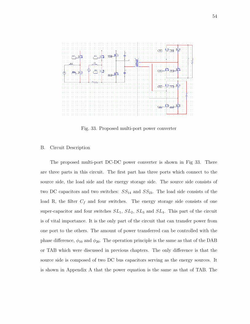
54
Fig. 33. Proposed multi-port power converter
B. Circuit Description
The proposed multi-port DC-DC power converter is shown in Fig 33. There
are three parts in this circuit. The first part has three ports which connect to the
source side, the load side and the energy storage side. The source side consists of
two DC capacitors and two switches: SS14 and SS23. The load side consists of the
load R, the filter Cf and four switches. The energy storage side consists of one
super-capacitor and four switches SL1, SL2, SL3 and SL4. This part of the circuit
is of vital importance. It is the only part of the circuit that can transfer power from
one port to the others. The amount of power transferred can be controlled with the
phase difference, φ10 and φ20. The operation principle is the same as that of the DAB
or TAB which were discussed in previous chapters. The only difference is that the
source side is composed of two DC bus capacitors serving as the energy sources. It
is shown in Appendix A that the power equation is the same as that of TAB. The

55
power equation for this part of circuit is:
P10 =V0V1
ωL10φ10(1 −
| φ10 |π
) (4.1)
P20 =V0V2
ωL20
φ20(1 −| φ20 |
π) (4.2)
P21 =V1V2
ωL21φ21(1 −
| φ21 |π
)P0 = P10 + P20 (4.3)
P1 = P10 + P12 (4.4)
P2 = P20 + P21 (4.5)
where
V0 = 0.5VDC
V1 is the referred voltage of the load side to the primary side.
V2 is the referred voltage of the energy storage side to the primary side.
P0 is the power delivered from the source side.
P1 is the power going into the load side.
P2 is the power into the energy storage side.
P10 is the power delivered from the source side to the load side.
P20 is the power delivered from the source side to the energy storage side.
P21 is the power delivered from the load side to the energy storage side.
The second part of the circuit consists of one voltage source, one inductor, two
switches, SP1 and SP2, and the DC bus capacitors. The voltage source can be a
renewable energy source. The function of this part of the circuit is that by controlling
the current of the inductor L0, the DC bus voltage VDC, which consists of two DC
bus capacitors, can be regulated. The reason for this is that the DC bus voltage
will decrease while these DC bus capacitors provide energy to the load side and
energy storage side. Therefore the voltage source behind the inductor has to provide

56
the proper amount of energy to support the DC bus voltage such that the DC bus
voltage can be kept constant. The reason why DC bus voltage has to be kept constant
will be elaborated later.
The third part is exactly the same as the second part, which consists of one
voltage source, one inductor L1, and two switches, SPP1 and SPP2. However, the
purpose of the third part is that it will integrate another renewable energy source and
regulate its output power at a fixed value, which is specified by the central controller.
If this renewable energy source is a voltage source, the power from this source can
be controlled by controlling the current flowing in the inductor L1. If the source is a
current source, the inductor L1 has to be removed and the power can be controlled
by duty ratio(D) control. The power of the third part can be calculated with the
following equations:
Pin1 = Vin1 · IL1 for voltage source (4.6)
Pin1 = (DVDC) · Iin1 for current source (4.7)
C. Design of Proposed Multi-port Power Converter
There are several components to be designed, including the transformer turn
ratio, the leakage inductor of the transformer, the input inductors, the DC bus ca-
pacitor, the energy storage capacitor, the load filter capacitor, and the current rating
and voltage rating of the switches.
Table IV shows the specs of the proposed circuit, which is given for the design
process.

57
Table IV. Specs of the proposed circuit
parameter symbol value unit
DC bus voltage VDC 108 Volt
Primary energy source voltage Vin0 54 Volt
Auxiliary energy source voltage Vin1 50 Volt
Energy storage capacitor voltage VC 54 Volt
Switching frequency fs 5 KHz
Load Power Pload 1000 ±10% Watt
Load Voltage Vload 155:115 (135) Volt
Primary energy source power Pin0 1000 Watt
Auxiliary energy source power Pin1 500:50 (300) Watt
1. Transformer Turn Ratios
To minimize the current on the leakage inductor of the transformer, the voltage
on both side of the leakage inductor should be the same. This can be seen from the
derivation in Appendix A. Therefore, the turn ratios are:
n1 =135
54= 2.5 (4.8)
n2 =1
1= 1 (4.9)
2. Leakage Inductance of Transformer
Assume that all the load power is provided by the energy source, not from the
energy storage capacitor. Therefore, P10 will be 1000 W. From Equation (4.1), the
smaller the inductor L10 ,the greater the power transferred with the same phase φ10.
However, if the inductor is too small, the current rating of the inductor will be large.

58
A trade-off has to be made. Therefore, φ10 is designed to be around 20o when P10 is
1000 W. Then L10 can be found to be 30 µH. In the same way, L20 and L12 can be
designed. From Eq. 3.7 to 3.21 , the value of l1, l1 and l2 can be calculated.
3. Output Filter Capacitor
The current flowing into the load side, which is port 1, has DC value and some
harmonics. To have a constant load voltage, a filter capacitor needs to be connected
in parallel with the load resistor. The conductances of these two components are:
GCf= −j2πfCf (4.10)
GRload=
1
Rload
(4.11)
To filter out the harmonic current, GCfshould be large enough at frequency f so
that the harmonics of frequency f will flow into the filter capacitor Cf . In this way,
there will be DC current flowing in the load resistor, making the load voltage almost
constant. Since the switching frequency fs is 5000 Hz, and R is about 18 Ω when the
output power is 1000W, Cf is selected to be 1mF such that the conductance of Cf at
the switching frequency is about 500 times the conductance of R.
4. Input Inductor L0, L1
There are two requirements for designing the input inductors. First, the current
ripple of inductor current should be small since the inductor current is the output
current of the renewable energy sources. It is desirable for renewable energy sources
to have small current ripple. However, since the inductor current is also a control
variable controlled by the central controller, if the inductance is too large, it takes a
longer time to change the inductor current, resulting in slow dynamics. There is a
tradeoff to be made.

59
Since ”constant-frequency control with turn-on at clock time” current control
method is used, the switching time of the switches is not fixed. It depends on the
current in the inductor. Therefore, the worst case design will be performed. The
worst case is that the switch SP1 or SPP1 are turned on during the whole period. If
the allowable current ripple for IL0 is 1A, the following equations is used:
∆IL0 =Vin0
L0(
1
fs
) (4.12)
The value of L0 is designed to be 10mH.
The allowable current ripple for IL1 is 0.1 A. With the same method, the value
of L1 is 54mH.
5. DC Bus Capacitor CDC
The DC bus voltage should remain at constant value. In triple active bridge,
there will be some energy in the DC bus capacitor going into the other two ports,
which are the load and the energy storage. In order to maintain the DC bus voltage,
the renewable energy source has to provide the necessary energy to the DC bus
capacitor. In the control mechanism that regulates the DC bus voltage, discussed
in a later section, the energy provided by these energy sources is first stored in the
input inductor L0. Then this energy will be transferred to the DC bus capacitors by
resonance. However, the resonance time constant is set much longer that the period of
the switching speed of the switch. In this way, the DC bus voltage can be controlled
without going through the entire cycle of resonance. The current in the inductor
remains almost constant with some ripple while the voltage in the DC bus capacitor
is regulated with some ripple. To have a stiff DC bus, the capacitance of the DC bus
capacitors should be larger than the inductance of the input inductors. The ripple of
the DC bus voltage will be smaller than the ripple of the inductor current. Therefore,

60
the capacitance of the DC bus capacitors is designed to be 0.1 F.
6. Energy Storage Capacitor
The size of the energy capacitor depends on several requirements: 1) the input
power from the two renewable energy sources, 2) the load power, 3) the allowable
range of voltage for energy storage capacitors. By using the concept of energy con-
versation, the size of energy capacitor can be designed.
The time of proper operation for different conditions can be calculated as follows:
T =12C(V 2
cmax − V 2cmin)
Pinput−total − Poutput − Ploss
(4.13)
Table V shows the duration of operation for different conditions, assuming that Pin0
and Pin1 are all constant. No central controller is used to control Pin1. In the table,
if the time T is positive, it means the energy capacitor is being discharged, that is,
providing energy. If the time T is negative, it means the energy capacitor is being
charged, that is, absorbing energy.
7. Current and Voltage Rating of Switches
Because the inductor current in the energy source side is controlled by the current
controller, which will be mentioned in the later section, the current rating of the
switches SP1, SP2, SPP1, SPP2 is related to the current command range. The
current rating of the switches connected to the transformer depends on the current
flowing in the transformer. The current in the transformer depends on the phase
differences and turn ratios. If the range of phase differences is known and the turn
ratios are designed, the current flowing in the transformer can be found. As for the
voltage rating, it depending on the voltage source to which the switches are connected
to. Table VI summarizes the rating of all switches.

61
Table V. Operation time for different conditions
Vload=135 V, Pin0=1 kW, Pin1=100 W
Pload = 1200W Pload = 1000W Pload = 856.8W
T = 7.7088s T = -18.99s T = -5.471s
Vload=155 V, Pin0=1 kW, Pin1=100 W
Pload =1582.7W Pload =1318.2W Pload = 1129.5W
T = 2.0961s T = 4.2252s T = 15.35s
Vload=115 V, Pin0=1 kW, Pin1=100 W
Pload = 871.2W Pload = 725.6W Pload =621.7W
T = -5.892 s T = -3.3108 s T =-2.5222 s
D. Modeling of Proposed Multi-port Power Converter
The reason why modeling is important is that with the mathematical models, the
controller of this power converter can be designed more efficiently, instead of using
lots of trial and error. Also, with the mathematical models, some analysis can be
done, such as stability issues at different operating points. The issue of stability will
be discussed later.
Before modeling the circuit, there is one question we need to ask. What do we
do with this circuit? The purpose of this circuit is to integrate two energy sources,
one energy storage and one dynamic load. What do we mean by integrate? Here is
the problem statement:
Under the influence of dynamic load, the load voltage Vload and the
output power from the renewable energy sources Pin0 and Pin1 are regulated
or controlled.

62
Table VI. Voltage rating and current rating of all switches
voltage rating (V) current rating (A)
SP1 VDC IL0
SP2 VDC IL0
SPP1 VDC IL1
SPP2 VDC IL1
SS14 0.5 VDC 150
SS23 0.5 VDC 150
SL1 Vload 60
SL2 Vload 60
SL3 Vload 60
SL4 Vload 60
SC1 VC 150
SC2 VC 150
SC3 VC 150
SC4 VC 150
This problem can be solved by controlling two variables: φ10 and φ20. Two PI
controllers will be used for φ10 and φ20, and the feedback signals are load voltage,Vload,
and the output power from the source side, P0. Due to the above requirement, the
mathematical models are needed between the Vload and φ10, and between P0 and φ20.
In power electronics, state space averaging technique is widely used to derive
transfer functions. However, in this work it can not be applied because the current
of the leakage inductor of the transformer varies substantially. The large variation
of current does not meet the requirement of state space averaging technique, where

63
it requires that all the state variables, including the voltage of capacitors and the
current of inductors, should have small variation. Therefore, another method of
deriving transfer functions has to be found.
Because the equation is non-linear, which will be seen shortly, the method of
perturbation and linearization are used during the derivation of transfer functions.
1. Transfer Function of v1
The power going into port 1, P1, can be found as the sum of the power going
into port 1 from port 0, P10, and the power going into port 1 from port 2, P12. P10
and P20 can be expressed as:
p10 =v0v1
ωL10φ10(1 − φ10
π) (4.14)
p12 =v1v1
ωL12φ12(1 − φ12
π) (4.15)
where v1 and v2 are the referred voltages to the primary side of the load voltage vload
and the energy storage capacitor voltage vc.
From this equation, it can be seen that the system is a nonlinear system. In order
to find the transfer function, perturbation and linearlization have to be applied.

64
Assuming that the operating points are:
v0 = V0
v1 = V1
v2 = V2
φ10 = Φ10
φ20 = Φ20
Now the perturbation signals are added into the above variables. Since v0 is normally
the constant in our application, there is no perturbation in v0.
v1 = V1 + v1
v2 = V2 + v2
φ10 = Φ10 + φ10
φ20 = Φ20 + φ20
65
Therefore,
p1 = p10 + p12 =v0v1
ωL10φ10(1 − φ10
π) +
v1v2
ωL12φ12(1 −
φ12
π)
= [V0(V1 + v1)
ωL10· (Φ10 + φ10) · (1 − Φ10 + φ10
π)]
+ [(V1 + v1)(V2 + v2)
ωL12
· (Φ10 − Φ20 + φ10 − φ20) · (1 − Φ10 − Φ20 + φ10 − φ20
π)]
=(V0V1
ωL10
Φ10 +V0V1
ωL10
φ10 +V0v1
ωL10
Φ10 +V0v1
ωL10
φ10]
− [V0V1
ωL10
Φ10 +V0V1
ωL10
φ10 +V0v1
ωL10
Φ10 +V0v1
ωL10
φ10] ·Φ10
π
− [V0V1
ωL10Φ10 +
V0V1
ωL10φ10 +
V0v1
ωL10Φ10 +
V0v1
ωL10φ10] ·
φ10
π
)
+V1V2 + V1v2 + V2v1 + v1v2
ωL12[Φ10 − Φ20 + φ10 − φ20]
+V1V2 + V1v2 + V2v1 + v1v2
ωL12π[Φ10 − Φ20 + φ10 − φ20]
2
After simplification and reduction, the following can be found:
p1 =[
(V0Φ10
ωL10
− V0Φ210
ωL10π) + (
Φ10 − Φ20
ωL12
+(Φ10 − Φ20)
2
ωL12π)V2
]
v1 (4.16)
+[
(V0V1
ωL10− 2V0V1Φ10
ωL10π) +
V1V2
ωL12− 2V1V2(Φ10 − Φ20)
ωL12π
]
φ10
+[Φ10 − Φ20
ωL12V1 −
(Φ10 − Φ20)2
ωL12πV1
]
v2
+[−V1V2
ωL12
+2V1V2(Φ10 − Φ20)
ωL12π
]
φ20
= a · v1 + b · phi10 + c · v2 + D · φ20

66
where
a(V0, V1, V2, Φ10, Φ20) = (V0Φ10
ωL10− V0Φ
210
ωL10π) + (
Φ10 − Φ20
ωL12+
(Φ10 − Φ20)2
ωL12π)V2 (4.17)
b(V0, V1, V2, Φ10, Φ20) = (V0V1
ωL10
− 2V0V1Φ10
ωL10π) +
V1V2
ωL12
− 2V1V2(Φ10 − Φ20)
ωL12π(4.18)
c(V0, V1, V2, Φ10, Φ20) =Φ10 − Φ20
ωL12
V1 −(Φ10 − Φ20)
2
ωL12πV1 (4.19)
d(V0, V1, V2, Φ10, Φ20) =−V1V2
ωL12+
2V1V2(Φ10 − Φ20)
ωL12π(4.20)
On the other hand, the power going into the load side P1 can also be expressed
as:
p1 = P1 + p1 =(V1 + v1)
2
R+
d
dt
(1
2Cf · (V1 + v1)
2)
(4.21)
After simplification, p1 can be expressed as:
p1 =2V1
Rv1 + CfV1
d
dtv1 (4.22)
Using the Laplace transform, the above equation can be written as:
p1 =2V1
Rv1 + s · CfV1v1 (4.23)
= (s · CfV1 +2V1
R)v1
From (4.16) and (4.23), v1 can be expressed as:
v1 =b
s · CfV1 + 2V1
R− a
· φ10 +d
s · CfV1 + 2V1
R− a
· φ20 +c
s · CfV1 + 2V1
R− a
· v2
(4.24)
= A · φ10 + B · φ20 + C · v2 (4.25)

67
2. Transfer Function of P0
In the similar way, the transfer function of P0 can be derived as follows:
p0 = p10 + p20 =v0v1
ωL10
φ10(1 − φ10
π) +
v0v2
ωL20
φ12(1 − φ20
π)
= [V0(V1 + v1)
ωL10· (Φ10 + φ10) · (1 −
Φ10 + φ10
π)]
+ [V0(V2 + v2)
ωL20· (Φ20 + φ20) · (1 −
Φ20 + φ20
π)]
After the simplification and reduction, we get,
p0 = [V0Φ10
ωL10− V0Φ
210
ωL10π] · v1 + [
V0V1
ωL10− 2Φ10V0V1
ωL10π] · φ10 (4.26)
+ [V0Φ20
ωL20− V0Φ
220
ωL20π] · v2 + [
V0V2
ωL20− 2Φ20V0V2
ωL20π] · φ20
= D · v1 + E · φ10 + F · v2 + G · φ20
where
D(V0, V1, V2, Φ10, Φ20) =V0Φ10
ωL10
− V0Φ210
ωL10π(4.27)
E(V0, V1, V2, Φ10, Φ20) =V0V1
ωL10
− 2Φ10V0V1
ωL10π(4.28)
F (V0, V1, V2, Φ10, Φ20) =V0Φ20
ωL20− V0Φ
220
ωL20π(4.29)
G(V0, V1, V2, Φ10, Φ20) =V0V2
ωL20− 2Φ20V0V2
ωL20π(4.30)
In (4.24) and (4.26), there are two points worthy of attention. First, the relation-
ship between vload and φ10 and the relationship between p0 and φ20 are not simple.
They are coupled. φ20, v2 have effect on v1. Also, φ10, v1 and v2 also have impact on
p0. Fig 34 shows the coupling between the variables.
Secondly, the coefficients in (4.24) and (4.26) depend on the operating points V0,
V1, V2, Φ10 and Φ20. These coefficients change as the operating points change. In

68
A
B
C
E
G
F
~V 2
+
+
D
~£X 10 ~V 1
~P 0
~£X 20
Fig. 34. Transfer function of the system
order to use these transfer functions, the operating points have to be found first.
3. How to Find the Operating Point
In normal operation, the power from port 0 will be equal to the power into port
1. In other word, the power into the energy storage C from the source side will be
equal to the power into the load side from the energy storage C. The net power of C
is zero. The above condition can be expressed as follows:
P1 = P0
P20 = P12
We can see from Fig 35 that P1 consist of two part: one is P10, the other is P12. We
have to find out the ratio of P10 to P12 so that the operating point Φ10 and Φ20 can
be calculated.
The given value will be P1 and we need to find the ratio Q. First, we set the ratio

69
Fig. 35. Power flow between 3 ports
Q as 1. Then P10 can be found as:
P10 = P1 · Q =V0V1
ωL10Φ10(1 − Φ10
π)
Φ10 can be solved.
As soon as Φ10 is found, Φ20 can be solved from the following equation:
P20 = P12
V2V0
ωL20Φ20(1 − Φ20
π) =
V1V0
ωL12(Φ10 − Φ20)(1 − Φ10 − Φ20
π)
When both Φ10 and Φ20 are known, P1 can be calculated from:
P1−cal = P10 + P12
=V0V1
ωL10φ10(1 − φ10
π) +
V1V2
ωL12φ12(1 − φ12
π)
Compare P1−cal and P1. If the error is not within the limit, decrease the ratio Q and
do the above procedure again till the error is within the satisfactory range. The flow
chart of finding the operating point is shown in Fig 36.

70
Specify the load power
P 1
Ratio=1
P 10 =P 1 *Ratio
With P 10 =P 1 *Ratio find phi 10
With P 20 = P 12 find phi 20
With phi 10 and phi 20
f ind P 1_cal
| P 1 -P 1_cal | < error
Decrease the Ratio
yes
No
Output phi 10 and phi 20
Fig. 36. Flow chart for finding operating point: Φ10 and Φ20
E. Control of Proposed Multi-port Power Converter
After the model of the system is obtained, the controllers can be designed. In
this proposed circuit, there are several things to be controlled. The purpose of the
control is, under the influence of dynamic load, to 1) regulate or control the load
voltage Vload and 2) regulate or control the input power from these two renewable
energy sources. To achieve this purpose, there are several controls that need to be
done. The first one is to use φ10 and φ20 to control the load voltage, Vload, and the
input power from the primary side, P0. The second one is to regulate the DC bus
voltage, VDC . The third one is to control the current, IL0 and IL1, flowing in the two

71
energy sources. How to design the controller for φ10 and φ20, how to regulate VDC ,
and how to control IL0 and IL1 will be discussed in the section.
1. Controller Design for φ10 and φ20
The transfer functions of φ10 to Vload and of φ20 to P0 were found in the previous
section. However, the transfer functions are complicated. They are coupled, and
their coefficients depend on the operating points. It seems like the system is hard to
control.
However, if the operation points are found according to the normal operation,
where Vload is 135V, P0 is 1000 W, the coefficient of these transfer functions can be
found. Fig. 37 shows the transfer functions when the system operates at normal
operation.
5498 ---------------- 0.33s + 17.17
-2864 ---------------- 0.33s + 17.17
6.437 ---------------- 0.33s + 17.17
2634
2863
6.44
~V 2
+
+
12.38
~£X 10 ~V 1
~P 0
~£X 20
Fig. 37. Transfer function of TAB under normal condition

72
From this graph, it can be seen that some coefficients are much larger than other
coefficients. Therefore, it is logical to say some variables are more influential than
some other variables. In this case, the coefficient of the transfer function from v2 to
v1 is much smaller than that from φ10 to v1 and from φ20 to v1. Also, the coefficient of
the transfer function from v2 to p0 and from v1 to p0 is much smaller than that from
φ10 to p0 and from φ20 to p0. Therefore, the impact of v2 on v1 and p0 can be ignored.
The above arguments simplified the transfer functions of the system as shown in Fig
38.
5498 ---------------- 0.33s + 17.17
-2864 ---------------- 0.33s + 17.17
2634
2863
+
+
~£X 10 ~V 1
~P 0
~£X 20
Fig. 38. Simplified transfer function of TAB
Since the simplified transfer functions are obtained, it is possible to design the
controllers to meet certain performance requirements. However, due to the coupling,
it is hard to design controllers by using conventional methods. Most designing meth-
ods are for single-input-single-output systems. There are many literatures on how

73
to design controllers for multi-input-multi-output coupled systems. In this work the
method, proposed by He, Mao-Jun [22], is adopted. The procedure for this method is
shown in Fig 39. The concept is simple. In this method, the controllers are designed,
first, without considering the effect of coupling. Then, depending on the effects of
coupling between variables, the procedure detunes the parameters of these controllers
to make the system stable. The effects of coupling between variables are measured
by the matrix called dRI. This method ensures this feedback system be stable.
Pair input and outputs
Design controller for uncoupled system
Construct P
Set i=1
Calculate the critical frequency w cri
Calculate dRI £p ii,n-1
Calculate k £li,n-1 and £c £li,n-1 for MMF £l i,n-1
Calculate detuning factor f ki and f £ci
Detuning controller parameters
i<n ?
i=i+1
End
Fig. 39. Design procedure for coupled systems
Due to the conservativeness of this method, the performance of the system is not
optimal. Therefore, several fine-tunings have to be done. In conclusion, this method
is used to get the approximate value of the parameters of these controllers, which will

74
facilitate the design process.
2. Current Control
There are several methods to control the current flowing in the inductors, in-
cluding:
• Tolerance band control,
• Constant-off time control,
• Constant-frequency control with turn-on at clock time.
The method adopted in this work is constant-frequency current control. The bene-
fits is that the operation frequency is fixed, which makes designing the filter easier
compared to the other methods of current control. [23]
When the time is at clock time, the switche, SP2 or SPP2, is turned on. As soon
as the current reaches the specified value, the switche, SP2 or SPP2, is turned off and
switche, SP1 or SPP1, is turned on. This will result in the decrease of the current.
This will last during the rest of the period. Till the time is at clock time, SP1 or
SPP1 is turned off and SP2 or SPP2 is turned on again. Then the procedure repeats.
Fig. 40 shows the circuit when switches are turned on and off. Fig. 41 shows the
current waveform during the current control, and Equation 4.31 and 4.32 describe
the mathematical equations for these two different configurations.
dIL
dt=
Vin
Lwhen SP2 or SPP2 are turned on (4.31)
dIL
dt=
Vin − VDC
Lwhen SP1 or SPP1 are turned on (4.32)

75
Fig. 40. Inductor circuit during different time period
Fig. 41. Current waveform during the current control [23]
3. DC Bus Voltage Regulation
To regulate the DC bus voltage, the proposed system uses the switches, SP1 and
SP2, on the primary energy source. In this part of the circuit, shown in Fig. 42,
there are one voltage source, one inductor, two switches and two DC bus capacitors.
There are two ways to regulate the DC bus voltage. One is to use duty ratio control.
The other is to use current control. For duty ratio control, the DC bus voltage can
be regulated by controlling the duty ratio of the switches. From the analysis of power

76
Fig. 42. DC regulation circuit
electronics, the voltage gain for this circuit can be expressed as follows:
VDC
Vin1=
1
1 − D(4.33)
where D is the ratio of time to the period when SP2 is on.
With the feedback signal of VDC , one PI controller is used to give the duty ratio
command D to regulate the DC bus voltage. However, there are several shortcomings
for this method. The dynamic response is slow compared to the current control
method. Another shortcoming is that the current in the inductor may be large,
depending on the value of D. If the dynamics of PI is fast to strictly regulate the DC
bus voltage, the inductor current may be large, which is undesirable.
Another way to regulate the DC bus voltage is to use current control. The
inductor current is controlled by the method of constant-frequency control with turn-
on at clock time, as discussed in previous section. The current command is given by
the PI controller whose input signal is the reference DC bus voltage, and the feedback
signal of the PI controller is the DC bus voltage. After the PI controller, a limiter
is inserted before the current command goes into the current controller. With the

77
limiter, the peak inductor current can be confined. This method has better dynamic
performance, and ensures the current be within the allowable range as well. Fig. 43
shows the block diagram for the DC bus regulation.
PI Controller
V DC
V DC_ref Current
Controller Gate Drive of SP1, SP2
Fig. 43. Block diagram for DC voltage regulation
4. Control Strategy for Different Set of Switches
There are 14 switches in the proposed circuit. The switches on the load side
are SL1, SL2, SL3, and SL4. The switches on the energy storage side are SC1, SC2,
SC3, and SC4. The switches on the source side can be categorized into three groups:
SS14 and SS23 connecting the DC bus capacitor with the transformer; SP1 and SP2
connecting the primary energy source; and SPP1 and SPP2 connecting the auxiliary
energy source.
The control variables φ10 and φ20 control the gating signals of SS14, SS23, SL1,
SL2, SL3, SL4, SC1, SC2, SC3 and SC4. The hysteresis control of input power Pin1
controls the gating signals of SPP1 and SPP2. But what control strategy is applied
to SP1 and SP2?
From the transfer functions of the proposed circuit, the feedback signal for φ20
control loop should be the signal of P0. However, the value of P0 can not be measured
easily. Since the current flowing in the primary side of the transformer is oscillating
tremendously, it will be hard to find the average value of this current, which means
it will be hard to find the average power from the primary side. Even if it is possible
to measure the exact P0 and by feedback control, φ20 is controlled such that P0 is

78
regulated, it is possible that Pin0 is not regulated. Since
P0 = Pin0 + Pin1 + Pc (4.34)
If the DC bus voltage is not regulated, the value of Pc depends on the DC bus voltage
and its rate of change. This can be seen from the energy and power of the DC bus
capacitors:
Ec =1
2C · V 2
DC (4.35)
and
Pc =d
dtEc = C · VDC · dVDC
dt(4.36)
Therefore, the proposed control strategy will control the switch SP1 and SP2 to
regulate the DC bus voltage, VDC , such that Pc is almost zero. That is
Pc∼= 0 (4.37)
Also, the input power of the auxiliary source, Pin1 is regulated at constant value K
by hysteresis control.
Pin1 = K(constant) (4.38)
Therefore, P0 can be expressed as follows:
P0 = Pin0 + K (4.39)
From the above equation, it can been seen that Pin0 can be controlled by P0. Since
P0 is controlled by φ20, Pin0 can be indirectly controlled by φ20. This is the reason
why the proposed control strategy uses Pin0 as the feedback signal for the φ20 control
loop.

79
Table VII. The dependence of switches
Switches Dependence
SS14, SS23 , SL1, SL2, SL3, SL4 φ10
SC1, SC2, SC3, SC4 φ20
SP1, SP2 DC bus voltage regulation
SPP1, SPP2 input power Pin1 regulation
Table VIII. The feedback signal for different control variables
Feedback signal Controller
Vload φ10
P10 φ20
Table VII summarizes the control of all switches, and Table VIII lists the feedback
signal for φ10 and φ20.
5. Benefits of PI Controller
In this work, the operating points are found at first and, based on the operating
points, the controllers are designed. Because perturbation and linearlization are used
to derive the transfer functions of the system, the signal input for these transfer
functions should be small signals, namely, vload and p10.
However, the input to the phase shifting controllers is the whole signal, consisting
of the DC signal and the small signal. The DC signals are Φ10 and Φ20 while the small
signals are φ10 and φ20. The DC signals have to be derived first from the operating
points and then are added with small signals to produce the whole signals for the
phase shifting controllers.

80
There are two interesting points in the actual implementation of control. Since it
is impossible to get the small signals, which are ˜vload and p10, as the feedback signals.
The feedback signals are the whole signals, which are vload and p10. Therefore, the
reference signal to the feedback controller should be the reference DC signal, not 0.
This is shown in Fig. 44.
PI Controller (master)
0
~v load Gate
Driving Circuit
Multi-port Converter
PI Controller
(slave)
0
~P 10
ĵ 10
ĵ 20
~ 10
~ 20 20
10
PI Controller (master)
v load Gate
Driving Circuit
Multi-port Converter
PI Controller
(slave)
ĵ 10
ĵ 20
~ 10
~ 20 20
10
p 10
V load-ref
P 10-ref
Fig. 44. Signals for the feedback system
Another point worth mentioning is that Φ10 and Φ20 do not have to be calculated
precisely. Because of the integrator in the PI controllers, the PI controllers produce
proper value such that the whole signals φ10 and φ20 are correct for current operating
points. Because of the PI controllers, it is possible to go from one operating point
to another. Even though the value Φ10 and Φ20 are not correct for these different

81
operating points, the PI controllers will adjust φ10 and φ20 such that these two signals
contain certain DC values to give the correct whole signals for these different operating
points.
The only difference between having correct or incorrect value of Φ10 and Φ20 is
the time to reach steady state. If Φ10 and Φ20 are correct, it takes less time to reach
steady states. While Φ10 and Φ20 are incorrect, it takes longer time to reach steady
states.
F. Central Controller
In addition to the controller that controls the phases, φ10 and φ20, there is a
central controller in the proposed system. The central controller does the following
tasks.
• Gives control signal during the start-up process of the circuit
• Gives the power command to the auxiliary energy source
• Selects the controller for different load voltages
1. Starting of the Circuit
Before the circuit enters the normal operation, the circuit has to be started
first. During the start-up of the circuit, the central controller controls φ10 and φ20
to determine the power flow among the three ports. Also the central controller will
send the gating signals to the switches of the proposed circuit. By controlling these
switches, we can open or close some of the ports, which is very important during the
starting procedure.
There are two cases for starting. In the first case, some energy storage compo-
nents have been energized, including the DC bus capacitors and the energy storage

82
capacitor. This scenario may be encountered when the circuit is connected to the grid,
and there are some external circuits that pre-charge these capacitors. In the second
case, all the energy storage components are relaxed. No energy is stored in these
components. This scenario may be encountered when the circuit is stand-alone. All
the energy is provided by renewable energy sources, and no external energy sources
or charging circuits exist.
Some components are energized
Before the circuit is started, the voltage of the DC bus capacitors, VDC, and the
voltage of the energy storage capacitor, VC , are set up, which is easily done by first
charging these capacitors to specified voltages by external circuits and connecting
these capacitors to the proposed circuit. Except the above components, all other
components are relaxed. These components including the filter capacitor, Cload, the
input inductors, L0 and L1, the leakage inductance of the transformer, Lleakage. The
following shows the state before starting the circuit.
VDC = 108 V
VC = 54 V
Vload = 0 V
IL0 = 0 A
IL1 = 0 A
Ileakage = 0 A
During the starting of the circuit, φ10 is set at 40 and the switches on the energy
storage side are all open. The above setting lets the power go from the energy source

83
side into the load side, charging the load capacitors. This value is constant, since φ10
is constant.
Because the inductor currents, IL0 and IL1, are zero at the beginning, the current
controllers of these two inductor currents close the switches SP2 and SPP2 to increase
these two inductor currents linearly. During this period, the DC bus voltage decreases.
This is because there is no energy supply from energy source and the two DC bus
capacitors supply the energy to the load side, charging the load capacitor. As soon
as the inductor currents reach the specified values, the hysteresis control of current
will begin to be executed.
When the capacitor on the load side is charged to specified value, the starting
process ends and this circuit enters the normal state. The PI controllers, which control
φ10, φ20 and IL0−cmd, begin to function and the circuit of the energy storage side gets
connected back to the system.
Fig. 45 shows the procedure during the starting of the circuit.
No components are energized
For an isolated power system, it is more practical to assume that all the components
are relaxed in the beginning. There is no charger to charge the capacitors. Therefore,
the energy sources of the proposed circuit have to charge these capacitors first before
the circuit begins the normal operation.

84
start up
All PI controller keep dormant
Disconnect Energy Storage
I L0_ref = 18.5 A I L 1_ref = 6 A Phase 10 =40
Vload <= 135V
yes
No
Connect the Eenrgy Storage PI controllers kick in
Fig. 45. Flow chart for starting the circuit
The following shows the state at the beginning.
VDC = 0 V
VC = 0 V
Vload = 0 V
IL0 = 0 A
IL1 = 0 A
Ileakage = 0 A
First, assume that the voltages of the renewable energy sources are rising linearly
with time in the beginning. After these voltages rise to certain value, they are constant
afterward. This is more practical since it takes time for renewable energy sources to
warm up. During the increase in the voltage of the renewable energy sources, the

85
inductor currents are also increasing due to current control. This step is quite similar
to the previous case. During this period, DC bus capacitors are also being charged
because the current of the inductors will flow into the DC bus capacitors.
As soon as the DC bus voltage reaches the specified level, the energy storage
capacitor begins to be charged. During this period, φ20 is set at certain value and
the secondary side of the transformer, which is connected to the load port, is shorted.
The reason for shorting the secondary side of the transformer is that even though the
gating signals for all IGBTs on the load side are open, there will be small current
flowing into the load side via these diodes. This part of the circuit is like a current
source rectifier, consisting of four diodes and a current source. As soon as the current
flows into the load side, some power goes into the load side, which greatly increase the
time required to charge the energy storage capacitors. There are two ways of shorting
the secondary side of the transformer. One way is to use a bidirectional current switch,
which is shown in Fig. 46. During charging the energy storage capacitor, this switch
is conducting. The current flowing on the secondary side of the transformer will flow
though this switch without providing power to the load side. Another method is by
closing the switches SL1 and SL2 or SL3 and SL4. In this way, the current on the
secondary side of the transformer will flowing in these two switches, without providing
power to the load. In this way, the time to charge the energy storage capacitor will
be greatly decreased.
There is another problem left. What is the value of φ20? The value is hard to
determine because when the energy storage capacitor is being charged, the power
provided by the renewable energy sources, which is related to the inductor current,
IL0 and IL1, is flowing into the energy storage side. Since the power absorbed by
the energy storage capacitor varies with the voltage of the energy storage capacitor
Vc, it is impossible to find a constant value φ20 such that the power provided by

86
Fig. 46. Bidirectional current switch connected on load side
the renewable energy sources is equal to the power absorb by the energy storage
capacitor. The power difference will cause the voltage fluctuation in the DC bus.
That is, the power difference will go into the DC bus capacitor. This is not desirable.
The constant voltage of DC bus is preferred for the proper operation of the proposed
circuit.
To solve this problem,a PI controller is used to find φ20. The feedback signal
is the DC bus voltage, and output signal is φ20. Since the larger φ20 is, the more
power will go from the source side to energy storage side, which will decrease the
DC bus voltage. Due to this relation, the coefficient of the PI controller needs to be
negative. This will make the variation of DC bus voltage small during the charging
of the energy storage capacitor.
As soon as the voltage of the energy storage capacitor reaches the specified level,
the energy storage capacitor is disconnected from the proposed circuit by opening all
the switches connecting the energy storage capacitor. φ10 is set at 40o to charge the
filter capacitor on the load side. After the filter capacitor is charged, this circuit will
enter the normal state. All PI controllers kick in and the energy storage capacitor is
connected back to the circuit.
Fig. 47 summarizes the starting procedure.

87
start up
All PI controller keep dormant
Disconnect the load side
Charge the load capacitor
Connect the Eenrgy Storage PI controllers kick in
Increase inductor currents Charge DC bus capacitor
Charge the energy storage capacitor
Fig. 47. Flow chart for starting the circuit with all components relaxed
2. Power Management
According to the voltage of the energy storage capacitor, VC , the central con-
troller will give the corresponding power command to the auxiliary energy source. If
VC is too high, the central controller will decrease the power command of the auxil-
iary energy source to decrease the total input power, discharging the energy storage
capacitor. If VC is too low, the central controller will increase the power command
of the auxiliary energy source to increase the total input power, charging the energy
storage capacitor.
There are three levels of the power command for auxiliary energy source: 500W,

88
300W and 50W. The ranges of VC are 45-50, 50-60 and 60-65V. Intuitively, the cor-
responding input power command should be 500W(Pmax), 300W (Pnormal) and 50W
(Pmin) respectively. However, if we determine input power command just depending
on what VC is, there will be oscillation when the VC is closed to the turning point. To
solve this problem, not only the value of VC , but also the current input power com-
mand have to be considered. For different current input and different power command
for the auxiliary energy source, the new input power command will be different even
if the VC range is the same. Fig. 48 shows the corresponding input power command
under different conditions.
Fig. 48. Input power command Pin1 for different conditions
3. Controller Scheduling
The last thing the central controller does is to select the corresponding controller,
depending on the load voltage, Vload. This is called ”controller scheduling.”
Up to this point, the control purpose of the proposed circuit is to regulate the
load voltage, Vload. Is it possible that the load voltage can be controlled to be different
value? This problem will be controlling problem, instead of regulating problem.
If the stability analysis, which will be discussed in the next section, is performed,

89
it can be seen that the stability is good for a range of Vload. If we sweeping the Vload,
from 135V to 155V, the poles of the closed loop system will be on the left half plane.
Therefore, the designed controller is able to control the load voltage without being
unstable. However, because the controller is designed with the normal load voltage,
which is 135V, the performance for different load voltage will be not as good as that
for the case where load voltage is 135V.
In order to improve the performance for different load voltages, the concept of
”controller scheduling” is used in this work. There are three sets of controller, which
control the value of φ10 and φ20. These three sets of controllers are designed for each
different load voltage. Table IX shows the corresponding controller for each load
voltage.
Table IX. Controller scheduling
Load voltage command Controllers
115 V C11, C21
135 V C12, C22
155 V C13, C23
The central controller will choose the corresponding controller, depending on the
load voltage command. In this way, the dynamics for each load voltage command
will be better. Fig 49 shows the block diagram for controller scheduling.
G. Stability Analysis
From (4.24) and (4.26), the coefficients depend on the operating points. For the
dynamic load, the value of R is changing, resulting the change of the coefficients.
Also, during the operation, the voltage of the energy storage capacitor, VC , changes,

90
C 11
C 12
C 13
+/-
+/-
C 21
C 22
C 23
V load_ref
V load
P in0_ref
P in0
Selector
V load_ref
Gate Drive
Fig. 49. Block diagram for controller scheduling
depending on the power difference between the source and the load. The question
regarding the stability of the system arises. Will the change of R due to the dynamic
load let the system be unstable?
Because of the cross-coupling of the transfer function, the traditional way to
determine the stability due to the change of coefficient, such as Nyquist plot, Bode
plot is not practical. Fortunately, with the power of modern computer technology,
the poles of the system can be solved directly.
First, the transfer function of the coupled system need to be derived so that we
can use the traditional method to determine the stability of the system
The coupled system is represented in Fig. 50. The system can be represented by
Fig. 51. The function of g1 and g2 can be found by the following method.

91
g 11
g 21
g 12
g 22
C 1
C 2
+ +/-
+/-
+
x 2
x 1
y 1
y 2
u 1
u 2
Fig. 50. Transfer functions of coupled system
Since
y1 = u1 · g11 + u2 · g12 (4.40)
y2 = u2 · g22 + u1 · g21 (4.41)
and
u2 = −c2 · y2 = −c2 · (u2 · g22 + u1 · g21)
Therefore,
u2 =−c2 · g21
1 + c2 · g22· u1 (4.42)

92
g 1
C 1
C 2
+/-
+/-
x 2
x 1
y 1
y 2
u 1
u 2 g
2
Fig. 51. Simplified transfer function of coupled system
Combining (4.40) and (4.42), we get
y1 = (g11 +−c2 · g21 · g12
1 + c2 · g22)u1 (4.43)
= g1 · u1
where
g1 = g11 +−c2 · g21 · g12
1 + c2 · g22(4.44)
In the same way, we can found that
g2 = g22 +−c1 · g21 · g12
1 + c1 · g11(4.45)
As soon as g1 and g2 are calculated, the characteristic equation of the feedback
system can be found as:
Φ1(s) = 1 + c1 · g1 = 0 (4.46)
Φ2(s) = 1 + c2 · g2 = 0 (4.47)
The roots of the characteristic equations are the poles of the two feedback systems,
which are for the load voltage regulation and for the input power regulation. In order

93
to be stable, these poles have to have negative real part.
During the operation of the circuit, the operating points changes. It is necessary
to make sure that the system is stable during the operation. With the powerful
calculation capability of modern computers, it is easy to find all the poles for this
system by sweeping some variables. These variables include φ10, φ20, V2, and R. By
sweeping these variables in certain range, which depends on the actual operation, we
can find the stability of the system. Fig. 52 shows the poles of the closed loop, where
the sweep range for the variables are shown in Table X. In this graph, it can be seen
that all poles are on the left half plane. Therefore, the system is stable even though
the operating points changes during the operation of the circuit.
Table X. Sweeping range for variables
Variable Sweeping Range
φ10 0:15 (Degree)
φ20 0:15 (Degree)
V2 45:65 (V)
R 15:20 (Ω)
H. Integration of Current Source
Some renewable energy sources have the characteristic of current sources. They
will provide constant current while their output voltage varies. One example of re-
newable energy sources that has current source characteristics is photovoltaic cells.
The proposed circuit can integrate current source with little modification. Fig
53 shows the modified circuit. Assume that the current source provides Iin1 current.

94
Fig. 52. The poles of closed loop transfer functions under the sweeping of variables
The power provided by the current source can be controlled by the duty ratio of SPP1
and SPP2. If the duty cycle is defined as the on time of SPP1, then the power from
the current source can be expressed as:
Pin1 = D · Iin1 · VDC (4.48)
Since Iin1 and VDC are constant, the only way to control the power Pin1 is to control D.
Based on different power requirement, a table can be built to give the corresponding
D. To improve the control dynamics, a PI controller can be used, whose feedback
signal is power, while the output is duty ratio D. The block diagram is shown in Fig
54.

95
Fig. 53. Modified circuit to integrate current source
PI Controller Gate control for SPP1, and SPP2
P in1
P in1_ref Gate Drive D
Fig. 54. Block diagram of Pin1 control for current source

96
CHAPTER V
SIMULATION AND DISCUSSION
This chapter will present several simulations and discussion under different sce-
narios encountered in real application. In these simulations, the component values
are the values designed in the previous chapter. The input voltage of the renewable
energy source are 54V for Vin0 and 50V for Vin1. The nominal output load voltage
Vload is 135V and nominal input power, Pin0, is 1000W. The other input power, Pin1,
is controlled by the central controller to charge or discharge the energy capacitor.
A. Starting of the Circuit
If some energy storage components are initialy energized, the starting procedure
is easier. The initial voltage of the energy capacitor is 54V and the DC bus voltage is
108V. With the starting procedure described in the previous chapter, Vload increase,
shown in Fig 55 (c). As soon as Vload reaches 135V, the starting process stops, and the
two PI controllers kick in, shown by the two phase values φ10 and φ20 changing from
constant values to varying values at time=9ms. Also at the same time, the energy
storage is also connected back to the system, shown in the gating signal SC14. Fig
55 and Fig 56 show the simulation for this case.

97
Fig. 55. Starting with some component energized (a)IL0 and IL0−cmd [A], (b)IL1 and
IL1−cmd [A], (c) Vload [V], (d) φ10 and φ20 [degree]
Fig. 56. Starting with some component energized (a) φ10 and φ20 [degree] , (b)SP2,
(c) SPP2, (d)SC14

98
Another case for starting this circuit is that all components are relaxed. The
simulation results are shown in Fig 57 and Fig 58. In addition to charging the
output filter capacitor, the circuit has to charge the DC capacitors, the energy storage
capacitor. In the starting procedure expressed in Fig.47, the DC bus capacitor is first
charged to 108V with controlSS= controlSL= controlSC=0 and then energy storage
capacitor is charged to 54V with controlSS=1, controlSL=0, controlSC=1. Then the
output filter capacitor is being charged to 135V with controlSS=1, controlSL =1 and
controlSC=0. After that, the system exits the starting procedure and enters the
normal operation.
Fig. 57. Starting with all components relaxed (a)VDC [V], (b) VC [V], (c)Vload [V],
(d)controlSS, (e)controlSC , (f)controlSL

99
Fig. 58. Starting with all components relaxed (a)Pin0, Pin1 [W], (b)φ10 and φ20 [degree],
(c)Ileakage [A], (d)Isecond [A], (e)Itertiary [A]
B. Dynamics in Load
In this section, the load is changed at different time by changing the load resistor.
In Fig 59 and Fig 60, it can be seen that there are three levels of load, which are
1200W, 1000W and 800W. The controllers control the proposed circuit such that the
output voltage, Vload, is regulated and the input power from the renewable energy
sources, Pin0 and Pin1, remain constant regardless of the change of the load. The
difference of the input power, sum of Pin0 and Pin1, and load power, Pload is absorbed
by the energy storage capacitor. The voltage of energy storage capacitor shows that
there are some power going into and out of the energy storage capacitor. Also, from
the Fig. 60 (c) the current in the leakage inductor of the transformer is symmetric
due to the proper phase-shifting techniques.

100
Fig. 59. Simulation of dynamic load (a) Pload [W], (b) Pin0 and Pin1 [W], (c) Vload [V]
33
Fig. 60. Simulation of dynamic load (a) VC [V], (b) IL0 and IL1 [A], (c) Ileakage [A]

101
C. Large Dynamics in Load
Instead of small change in the load, in the following simulations, the load changes
tremendously. The load changes from normal load to two times of the load, changes
from normal load 1kW to 100W, change from normal load to 0W. The above cases
may be encountered in the stand-alone application, where short time over-ride or
short time no load are possible.
In Fig 61 and Fig 62, the load is increased from 1kW to 2kW at t=0.05 sec.
Before t=0.15, the regulation of Vload and Pin0 are quite good. Because the load
power increase to 2kW while the total input power is about 1.5kW, the deficit 500W
is supplied by the energy storage capacitor. Therefore, the voltage VC decreases very
fast. The function of control works fine until VC is too small. When VC is 0V at
t=0.18 sec, Pin0 tries to supply whole power required by load.
Fig. 61. Large increase in load power (a)Vload and VC [V], (b)Pin0 and Pin1 [W], (c)Pload
[W]

102
Fig. 62. Large increase in load power (a)φ10 and φ20 [degree], (b)IL0 and IL1 [A],
(c)Ileakage [A]
Fig. 63. Large decrease in load power (a)Vload and VC [V], (b)Pin0 and Pin1 [W], (c)Pload
[W]

103
Fig. 64. Large decrease in load power (a)φ10 and φ20 [degree], (b)IL0 and IL1 [A],
(c)Ileakage [A]
In Fig 63 and Fig 64, the load is decreased from 1kW to 100W at t=0.05 sec.
Before t=0.15, the regulation of Vload and Pin0 are quite good. Because the load power
decrease to 100W while the total input power is about 1.5kW, the extra 1400W is
absorbed by the energy storage capacitor. Therefore, the voltage VC increases very
fast. The function of control works fine even VC is way above the limit. But this is
not desirable. Extra large voltage can destroy the energy capacitor. Therefore there
exists limited time of operation for very low small load power.
Even the load power is reduced to 0W, the circuit works fine for short period
of time. From Fig 65 and Fig 66, the load power is reduced to 0W at 0.05sec. The
voltage VC increases very fast while Vload and Pin0 are kept at constant.

104
Fig. 65. Large decrease to no load (a)Vload and VC [V], (b)Pin0 and Pin1 [W], (c)Pload
[W]
Fig. 66. Large decrease to no load (a)φ10 and φ20 [degree], (b)IL0 and IL1 [A], (c)Ileakage
[A]
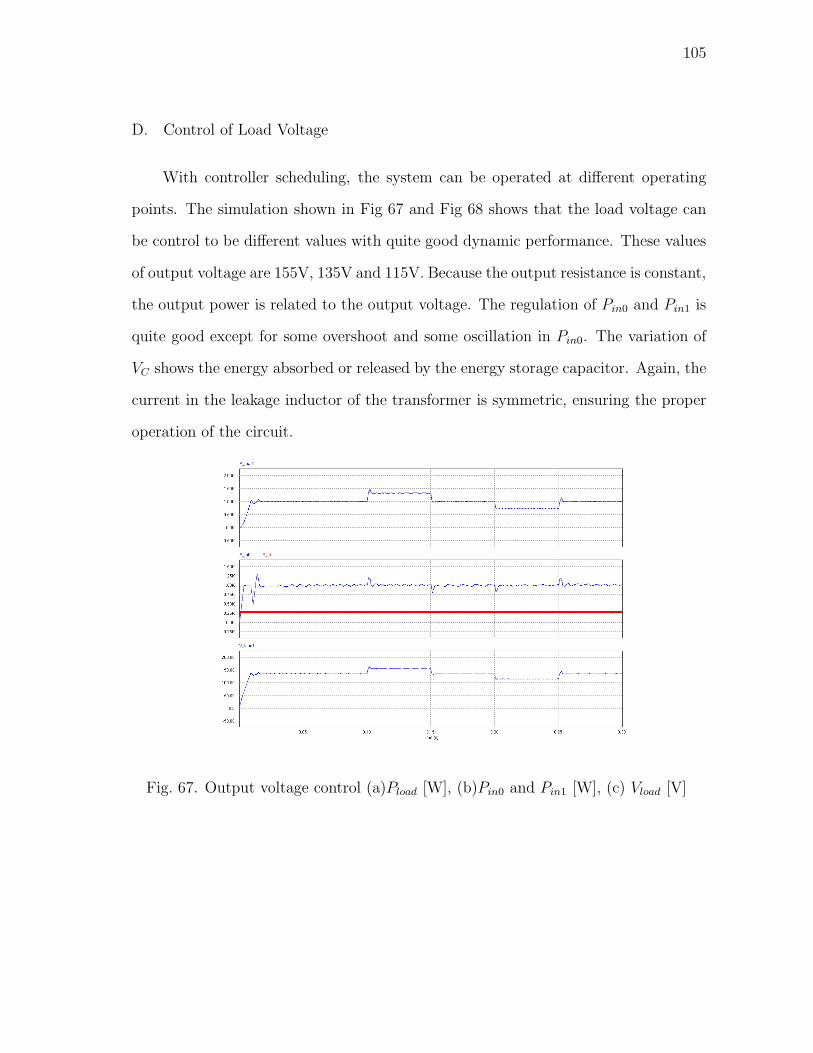
105
D. Control of Load Voltage
With controller scheduling, the system can be operated at different operating
points. The simulation shown in Fig 67 and Fig 68 shows that the load voltage can
be control to be different values with quite good dynamic performance. These values
of output voltage are 155V, 135V and 115V. Because the output resistance is constant,
the output power is related to the output voltage. The regulation of Pin0 and Pin1 is
quite good except for some overshoot and some oscillation in Pin0. The variation of
VC shows the energy absorbed or released by the energy storage capacitor. Again, the
current in the leakage inductor of the transformer is symmetric, ensuring the proper
operation of the circuit.
Fig. 67. Output voltage control (a)Pload [W], (b)Pin0 and Pin1 [W], (c) Vload [V]

106
Fig. 68. Output voltage control (a)VC [V],(b)IL0 and IL1 [A], (c)Ileakage [A]
E. Dynamics in Source
For renewable energy sources, the output power from these sources depends on
several factors, such as the wind speed, solar radiation, ambient temperature. The
proposed circuit shows the capability to make the output power constant under the
variation of input power of the input energy source. The difference of power is supplied
or absorbed by the energy storage capacitor. In Fig 69, the input power increases
from 1 kW to 1.5 kW while the load voltage and load power remain constant. The
extra power goes into the energy storage capacitor, resulting the increasing of VC .
In Fig 70, the input power decreases for 1 kW to 400 W while the load voltage and
load power also remain constant. The deficit power is supplied by the energy storage
capacitor. Therefore, the voltage of the capacitor VC is decreasing.

107
Fig. 69. Pin0 increases (a)Pin0 [W], (b)Pload and Pin1 [W], (c)Vload [V], (d)VC [V]
Fig. 70. Pin0 decreases (a)Pin0 [W], (b)Pload and Pin1 [W], (c)Vload [V], (d)VC [V]

108
F. Integration of Current Sources
In this simulation shown in Fig 71, the auxiliary energy source is a current source.
The power from the current source Pin1 is controlled at different values: 300W, 150W
and 350W. In this simulation, the load is changed at 0.075 second to 1.25kW and
changed back to 1kW at t=0.15 second. During the change of load, the Pin0 and Vload
are regulated at 1kW and 135V, respectively. This simulation shows that with the
integration of current source type energy source, the control of the circuit still works,
whose intend is to regulated load voltage Vload and primary input power Pin0.
Fig. 71. Different input power from current source (a)Pin1 and Pin1−cmd [W], (b)Vload
[V], (c)Pload and Pin0 [W]
G. Power Management
One of the roles of the central controller is to control the input powerPin1 from
the auxiliary energy source so that the voltage of energy storage capacitor VC remains
within a certain range. In this simulation in Fig 72, the capacitance of the energy

109
storage is reduced ten times so that it is easier to notice the voltage change of the
energy storage capacitor. When VC is below 45V, Pin1 is changed to 500W. When VC
reaches 60V, Pin1 is reduced so that VC won’t increase above the limit. At the same
time, the load power is changing at three levels, but the control requirements are still
met, which is to keep Vload and Pin0 at constant.
Fig. 72. Control of Pin1 (a)P load [W], (b)Pin0 and Pin1 [W], (c)Vload [V], (d)VC [V]

110
CHAPTER VI
CONCLUSION AND FUTURE WORK
A. Conclusion
In recent years, numerous investment and research have been put in renewable
energy. Because of inherent intermittent characteristics and slow response of renew-
able energy, energy storage has to be used in the system to provide the energy when
the energy from these renewable energy sources is low and supply when the energy
from these energy sources is high. In order to reduce the requirement of energy
storage, different kinds of renewable energy have to be integrated.
To integrate different renewable energy sources and energy storage devices, a new
multi-port DC-DC power converter is proposed because of the better performance,
lower cost, higher efficiency and system-level control.
The proposed circuit can integrate different renewable energy sources of differ-
ent voltage levels efficiently. Also the transformer in the circuit provides electrical
isolation between the source and the load. There are several desirable features of the
proposed circuit. This circuit can integrate voltage source type and current source
type of renewable energy sources effectively without any clamping circuits. Also un-
der wide range of different operating points, including normal load, large load, small
load, even no load, the system can remain stable and controlled. Furthermore, under
the fluctuation of power from the renewable energy sources, the load voltage can be
remained at constant.
This work first reviewed the previous work on ”Dual Active Bridge” and ”Triple
Active Bridge” to get some insight of the proposed circuit. In chapter four, the
description of fundamental operating principle was made. Design and Modeling were

111
made and based on the obtained transfer functions, the controllers were designed
accordingly. In addition to the low level control, central controller is used to deal
with various issues, including starting the circuit, maintaining the ”state-of-charge”
of the energy storage capacitor and selecting different controller for different operating
points. Also the stability and the robustness of the system were studied.
After simulations for different scenarios encountered in real application and some
dynamic stability test, it is shown that the proposed circuit is able to integrate renew-
able energy sources and energy storage economically and efficiently. Therefore the
proposed circuit will be an effective solution to the problem due to the intermittent
nature and slow response of the renewable energy.
B. Future Work
Because of the powerful capability of the proposed circuit, several applications
and extensions can be made. First, at the input side of the circuit, where renewable
energy sources are connected, some kinds of maximum power tracking techniques can
be done with the help of the central controller. By intelligently switching, based on
some maximum power tracking algorithm, the maximum power tracking can be made
for wind turbine and photovoltaic cells.
Another extension is to extend from three-port circuits to four-port or even five-
port circuits. Different ports are connected to different kinds of renewable energy
sources, whose voltage levels are different. Because there will be many phase dif-
ferences between these multiple ports, the interaction between these ports will be
complicated. How to deal with the interaction between ports and how to control
the power flow are challenging. With the technique of shorting of one port, used in
the starting procedure in this work, the interaction between different ports may be

112
reduced and can be controlled easily.
Another extension is to replace the energy storage capacitor with load. In this
topology, there will be two loads. With phase control, the two voltages at two different
outputs can be controlled independently, which may be of practical use for multi motor
drive application.
Instead of another load, another source can replace the energy storage capacitor
in this circuit. By controlling the phases, the power from source A to the load and
the power from source B to the load can be controlled independently as well. This
application is useful for load sharing application.
Therefore, the proposed circuit is suitable not only for the renewable energy
application, but also for the application of multi-source and multi-load application,
with little modification.

113
REFERENCES
[1] REN21 Steering Committee, (2007, June), “REN21 Renewables 2007 Global
Status Report,” Available: http:www.ren21.netdefault.asp
[2] U.S. Department of Energy, (2008, September), “Renewable Energy Data Book,”
Available: http:www1.eere.energy.govbapbadata books.html
[3] F. A. Farret and M. G. Simes, Integration of Alternative Sources of Energy, New
York: Wiley, 2006.
[4] P. Nema; R. K. Nema; S. Rangnekar, “A current and future state of art develop-
ment of hybrid energy system using wind and PV-solar: A review,” Renewable
and Sustainable Energy Reviews, vol.4, no.2, pp. 157-175, 2000.
[5] M. Ehsani; Y. Gao; S. E. Gay, Modern Electric, Hybrid Electric, and Fuel Cell
Vehicles: Fundamentals, Theory, and Design, Boca Raton, Florida: CRC, 2004.
[6] S. Jain; V. Agarwal, “An integrated hybrid power supply for distributed gener-
ation applications fed by nonconventional energy sources,” IEEE Trans. Energy
Conversion, vol.23, no.2, pp.622-631, June 2008.
[7] A. D. Napoli; F. Crescimbini; S. Rodo; L. Solero, “Multiple input dc-dc power
converter for fuel-cell powered hybrid vehicles,” Proc. IEEE Power Electronics
Specialist Conf., vol.4, pp.1685-1690, 2002.
[8] L. Solero; F. Caricchi; F. Crescimbini, O. Honorati; F. Mezzetti, “Performance
of a 10kW power electronic interface for combined windPV isolated generating
systems,” Proc. IEEE Power Electronics Specialist Conf., pp.1027-1032, June
1996.

114
[9] Y.M. Chen; Y.C. Liu; F.Y. Wu “Multi-input dc/dc converter based on the multi-
winding transformer for renewable energy application,” IEEE Trans. Ind. Appl.,
pp.1096-1104, 2002.
[10] R. D. Doncker; D. M. Divan; M. H. Kheraluwala, “A three-phase soft-switched
high-power-density DC/DC converter for high-power applications,” Industry Ap-
plications, IEEE Transactions on, vol.27, no.1, pp.63-73, Jan/Feb 1991.
[11] F. Z. Peng; H. Li; G-J Su; J. S. Lawler, “A new ZVS bidirectional DC-DC
converter for fuel cell and battery application,” Industry Applications, IEEE
Transactions on, vol.27, no.1, pp.63-73, Jan/Feb 1991.
[12] M. Michon; J. L. Duarte; M. Hendrix, “A three-port bi-directional converter for
hybrid fuel cell systems,” IEEE Power Electronics Specialists Conf., pp.4736-
4742, June 2004.
[13] D. Liu; H. Li, “A ZVS bi-directional DC-DC converter for multiple energy storage
elements,” IEEE Trans. Power Electronics, pp.1513-1517, Sept. 2006.
[14] R. L. Steigerwald; M. H. Kheraluwala, “High-frequency resonant transistor DC-
DC converters,” Industrial Electronics, IEEE Transactions on, vol.IE-31, no.2,
pp.181-191, May 1984.
[15] O. D. Patterson; D. M. Divan, “Pseudo-resonant full bridge DC/DC converter,”
Power Electronics, IEEE Transactions on, vol.6, no.4, pp.671-678, Oct 1991.
[16] K-H Liu, R. Oruganti, F-C Lee, “Resonant switches-topologies and character-
istics ,” presented at the 1998 IEEE Power Electron. Special Conf., Toulouse,
France.

115
[17] M. Ehsani, R. L. Kustom, Converter Circuit for Superconductive Magnetic En-
ergy Storage, College Station, Texas: Texas A&M Press, 1988.
[18] S. Singer, “Gyrators in power processing circuit,” Ind. Electron, IEEE Transac-
tions on, vol.IE-34, no.3, pp.313-318, Aug. 1987.
[19] H. Tao; A. Kotsopoulos; J. L. Duarte; M.A.M. Hendrix, “Design of a soft-
switched three-port converter with DSP control for power flow management in
hybrid fuel cell systems,” presented at the 2005 European Conf. on Power Elec-
tronics and Applications, Dresden, Germany.
[20] D. Xu; C. Zhao; H. Fan, “A PWM plus phase-shift control bidirectional DC-DC
converter,” Power Electronics, IEEE Transactions on , vol.19, no.3, pp. 666-675,
May 2004.
[21] M. Michon; J. L. Duarte; M. Hendrix; M.G. Simoes, “A three-port bi-directional
converter for hybrid fuel cell systems,” presented at the 2004 Power Electronics
Specialists Conf., Aachen, Germany.
[22] M-J He; W-J Cai; B-F Wu, “Design of decentralized IMC-PID controller based
on dRI analysis,” AlChE Journal, vol.52, no.11, pp. 3852-2863, Oct 2006.
[23] N. Mohan; T. M. Undeland; W. P. Robbins;, Power Electronics: Converter,
Applications, and Design, Boston: Wiley, 2002.

116
APPENDIX A
DERIVATION OF POWER EQUATION OF DAB AND TAB
In the DAB, the power equation can be found by averaging the current flowing in
the source side and the load side, because the voltage on the source side is DC value
while the voltage on the load side is almost constant with some ripple. The following
will show how to derive the power equation of DAB. There is one thing worth of
attention. The power derived here is the averaged power during the switching period,
which is a running average.
In the following derivation, V1 is assumed to be larger than V2 and the gating
signals of the load side lags that of the source side by φ. Fig 73 shows the waveform
of the circuit.
In order to find the average of input current, the time X needs to be find where
the current is crossing zero from negative to positive. The slope of the current when
the switch SS1 and SS4 are on is
m1 =V1 + V2
L(A.1)
and the slope of the current when the switch SS2 and SS3 are on is
m2 =V1 − V2
L(A.2)
The amplitude of the cuurent ix can be found as
∆ix =1
2[m1 · φ + m2 · (π − φ)] · T
2π(A.3)
=T
4πL(2V2φ + V1π − V2π)

117
We have to solve the following equation to get time X:
−∆ix + m1 · X = 0 (A.4)
X =2V2φ + (V1 − V2)π
2(V1 + V2)
T
2π
The length of y1 and y2 can be found as:
y1 = (φ − X) · m1 ·T
2π(A.5)
y2 = (π − φ) · m1 ·T
2π+ y1 (A.6)
The area of area 1, 2, 3 can be found as:
Area1 =1
2(φ − X) · y1 · (
T
2π)2 (A.7)
Area2 =1
2(π − φ) · (y1 + y2) · (
T
2π)2 (A.8)
Area3 =1
2X · y2 · (
T
2π)2 (A.9)
Total area will be:
Areatotal = Area1 + Area2 + Area3 (A.10)
=1
2
(
φy1 − Xy1 + y1π + y2π − φy1 − φy2 − Xy2
)
· ( T
2π)2
=1
2
(
(π − X)y1 + (π − φ − X)y2
)
· ( T
2π)2
Substitude y1, y2 and X, we will get the total area as:
Areatotal =V2
Lπφ(1 − φ
π)(
T
2π)2 (A.11)

118
Therefore, the average current will be
< Ix > =Areatotal
T2
(A.12)
=V2
ωL(1 − φ
π)
The power going out of the source port will be
< P >= V1· < Ix >=V1V2
ωL(1 − φ
π) (A.13)
For the case of triple active bridge(TAB), the power equation can be derived
similarly with the use of superposition theory.
For the proposed circuit, the power equation is the same as the ordinary TAB.
The only difference will be the V1 will be replaced by VDC/2.

119
V x
V y
V L
V 1
wt
wt
wt
wt
V 2
I L
I x
X
2
1
3 wt
y 1
y 2
phi
pi 2pi
phi
Fig. 73. Waveform of dual active bridge

120
VITA
Hung-ming Chou received his Bachelor of Electrical and Control Engineering
from National Chiao Tung University, Taiwan in 2004. After two years of military
service, he entered the graduate program in the Department of Electrical and Com-
puter Engineering at Texas A&M University and graduated in 2009. His research
interests include FACTS, HVDC, doubly-fed wind turbine, renewable energy integra-
tion, variable speed drive.
He can be reached at homing93@gmail or through his advisor Dr. M. Ehsani,
Power Electronics Laboratory, Department of Electrican and Computer Engineering,
Texas A&M University, College Station, Texas 77843-3128.