A High Step-up DC-DC Converter Based on the Voltage Lift ...
24
sustainability Article A High Step-up DC-DC Converter Based on the Voltage Lift Technique for Renewable Energy Applications Shahrukh Khan 1 , Arshad Mahmood 1 , Mohammad Zaid 1 , Mohd Tariq 1, * , Chang-Hua Lin 2, * , Javed Ahmad 2 , Basem Alamri 3 and Ahmad Alahmadi 3 Citation: Khan, S.; Mahmood, A.; Zaid, M.; Tariq, M.; Lin, C.-H.; Ahmad, J.; Alamri, B.; Alahmadi, A. A High Step-up DC-DC Converter Based on the Voltage Lift Technique for Renewable Energy Applications. Sustainability 2021, 13, 11059. https:// doi.org/10.3390/su131911059 Academic Editor: Pablo García Triviño Received: 27 July 2021 Accepted: 30 September 2021 Published: 7 October 2021 Publisher’s Note: MDPI stays neutral with regard to jurisdictional claims in published maps and institutional affil- iations. Copyright: © 2021 by the authors. Licensee MDPI, Basel, Switzerland. This article is an open access article distributed under the terms and conditions of the Creative Commons Attribution (CC BY) license (https:// creativecommons.org/licenses/by/ 4.0/). 1 Department of Electrical Engineering, ZHCET, Aligarh Muslim University, Aligarh 202002, India; [email protected] (S.K.); [email protected] (A.M.); [email protected] (M.Z.) 2 Department of Electrical Engineering, National Taiwan University of Science and Technology, Taipei City 10607, Taiwan; [email protected] 3 Department of Electrical Engineering, College of Engineering, Taif University, Taif 21944, Saudi Arabia; [email protected] (B.A.); [email protected] (A.A.) * Correspondence: [email protected] (M.T.); [email protected] (C.-H.L.) Abstract: High gain DC-DC converters are getting popular due to the increased use of renewable energy sources (RESs). Common ground between the input and output, low voltage stress across power switches and high voltage gain at lower duty ratios are desirable features required in any high gain DC-DC converter. DC-DC converters are widely used in DC microgrids to supply power to meet local demands. In this work, a high step-up DC-DC converter is proposed based on the voltage lift (VL) technique using a single power switch. The proposed converter has a voltage gain greater than a traditional boost converter (TBC) and Traditional quadratic boost converter (TQBC). The effect of inductor parasitic resistances on the voltage gain of the converter is discussed. The losses occurring in various components are calculated using PLECS software. To confirm the performance of the converter, a hardware prototype of 200 W is developed in the laboratory. The simulation and hardware results are presented to determine the performance of the converter in both open-loop and closed-loop conditions. In closed-loop operation, a PI controller is used to maintain a constant output voltage when the load or input voltage is changed. Keywords: high gain; low voltage stress; voltage lift (VL); renewable energy sources (RESs); equiva- lent series resistance (ESR) 1. Introduction The present alarming situation of depletion of non-renewable energy sources presents an opportunity to look for alternative energy sources. RESs are a good option to replace fossil fuel energy and nuclear energy for electrical power generation. In recent years, the share of RESs in power generation has increased significantly. Distributed generation (DG) technologies utilize RESs in the form of solar cells, fuel cells and wind turbines etc. [1,2]. To tackle the problem of environmental pollution and global warming caused by fossil fuels, sustainable energy production can be achieved by renewable [3,4] energy sources. Renewable energy systems and energy storage systems are going to play an important role in the future of low-carbon energy emission systems [5]. RESs are integrated with battery energy storage systems (BESSs), are not only envi- ronmentally friendly but also result in the wide use of DC (Direct Current) systems, i.e., DC generation and DC storage units. To inject this power into the alternating current (AC) Distribution Grid, DC-AC power electronic converters are used. Similarly, AC–DC and DC–AC conversion are used in AC drives. Moreover, the DC loads such as electric vehicles (EVs), light-Emitting Diode systems (LED), DC motors, data centres, and other battery-based devices are penetrating the market with a rising curve [6]. These systems require AC–DC conversion systems, so there are multiple stages of AC–DC conversion, Sustainability 2021, 13, 11059. https://doi.org/10.3390/su131911059 https://www.mdpi.com/journal/sustainability
-
Upload
khangminh22 -
Category
Documents
-
view
0 -
download
0
Transcript of A High Step-up DC-DC Converter Based on the Voltage Lift ...
sustainability
Article
A High Step-up DC-DC Converter Based on the Voltage LiftTechnique for Renewable Energy Applications
Shahrukh Khan 1 , Arshad Mahmood 1 , Mohammad Zaid 1, Mohd Tariq 1,* , Chang-Hua Lin 2,* ,Javed Ahmad 2 , Basem Alamri 3 and Ahmad Alahmadi 3
Citation: Khan, S.; Mahmood, A.;
Zaid, M.; Tariq, M.; Lin, C.-H.;
Ahmad, J.; Alamri, B.; Alahmadi, A.
A High Step-up DC-DC Converter
Based on the Voltage Lift Technique
for Renewable Energy Applications.
Sustainability 2021, 13, 11059. https://
doi.org/10.3390/su131911059
Academic Editor: Pablo García
Triviño
Received: 27 July 2021
Accepted: 30 September 2021
Published: 7 October 2021
Publisher’s Note: MDPI stays neutral
with regard to jurisdictional claims in
published maps and institutional affil-
iations.
Copyright: © 2021 by the authors.
Licensee MDPI, Basel, Switzerland.
This article is an open access article
distributed under the terms and
conditions of the Creative Commons
Attribution (CC BY) license (https://
creativecommons.org/licenses/by/
4.0/).
1 Department of Electrical Engineering, ZHCET, Aligarh Muslim University, Aligarh 202002, India;[email protected] (S.K.); [email protected] (A.M.); [email protected] (M.Z.)
2 Department of Electrical Engineering, National Taiwan University of Science and Technology,Taipei City 10607, Taiwan; [email protected]
3 Department of Electrical Engineering, College of Engineering, Taif University, Taif 21944, Saudi Arabia;[email protected] (B.A.); [email protected] (A.A.)
* Correspondence: [email protected] (M.T.); [email protected] (C.-H.L.)
Abstract: High gain DC-DC converters are getting popular due to the increased use of renewableenergy sources (RESs). Common ground between the input and output, low voltage stress acrosspower switches and high voltage gain at lower duty ratios are desirable features required in any highgain DC-DC converter. DC-DC converters are widely used in DC microgrids to supply power tomeet local demands. In this work, a high step-up DC-DC converter is proposed based on the voltagelift (VL) technique using a single power switch. The proposed converter has a voltage gain greaterthan a traditional boost converter (TBC) and Traditional quadratic boost converter (TQBC). Theeffect of inductor parasitic resistances on the voltage gain of the converter is discussed. The lossesoccurring in various components are calculated using PLECS software. To confirm the performanceof the converter, a hardware prototype of 200 W is developed in the laboratory. The simulation andhardware results are presented to determine the performance of the converter in both open-loop andclosed-loop conditions. In closed-loop operation, a PI controller is used to maintain a constant outputvoltage when the load or input voltage is changed.
Keywords: high gain; low voltage stress; voltage lift (VL); renewable energy sources (RESs); equiva-lent series resistance (ESR)
1. Introduction
The present alarming situation of depletion of non-renewable energy sources presentsan opportunity to look for alternative energy sources. RESs are a good option to replacefossil fuel energy and nuclear energy for electrical power generation. In recent years, theshare of RESs in power generation has increased significantly. Distributed generation (DG)technologies utilize RESs in the form of solar cells, fuel cells and wind turbines etc. [1,2].To tackle the problem of environmental pollution and global warming caused by fossilfuels, sustainable energy production can be achieved by renewable [3,4] energy sources.Renewable energy systems and energy storage systems are going to play an important rolein the future of low-carbon energy emission systems [5].
RESs are integrated with battery energy storage systems (BESSs), are not only envi-ronmentally friendly but also result in the wide use of DC (Direct Current) systems, i.e.,DC generation and DC storage units. To inject this power into the alternating current(AC) Distribution Grid, DC-AC power electronic converters are used. Similarly, AC–DCand DC–AC conversion are used in AC drives. Moreover, the DC loads such as electricvehicles (EVs), light-Emitting Diode systems (LED), DC motors, data centres, and otherbattery-based devices are penetrating the market with a rising curve [6]. These systemsrequire AC–DC conversion systems, so there are multiple stages of AC–DC conversion,
Sustainability 2021, 13, 11059. https://doi.org/10.3390/su131911059 https://www.mdpi.com/journal/sustainability
Sustainability 2021, 13, 11059 2 of 24
which reduce the overall efficiency and reliability of the systems. The increasing demandfor DC power at load has challenged the conventional AC distribution system, while theDC power systems are used for the transfer of DC power over long distances, mostly inhigh-voltage applications. The advantages of DC power systems have not been exploitedin low voltage (LV) (1.5 kV) and medium voltage (MV) (50 kV), leaving the power systemdomain to AC architecture [6,7]. To solve this problem, the concept of a DC microgrid isderived to meet local demands. Microgrids are interconnected to LV and MV distributionnetworks via direct connection or a power electronic interface. Easier integration of RESsand BESSs with DC microgrid means that the supply does not need to be converted intoAC; instead of the multiple AC–DC and DC–AC converter, DC power could be suppliedby a DC-DC converter, resulting in the reduction of primary energy consumption, leadingto efficient and smaller systems. Therefore, it is more efficient to have a DC distribution,including DC-DC converters, than AC counterparts [8].
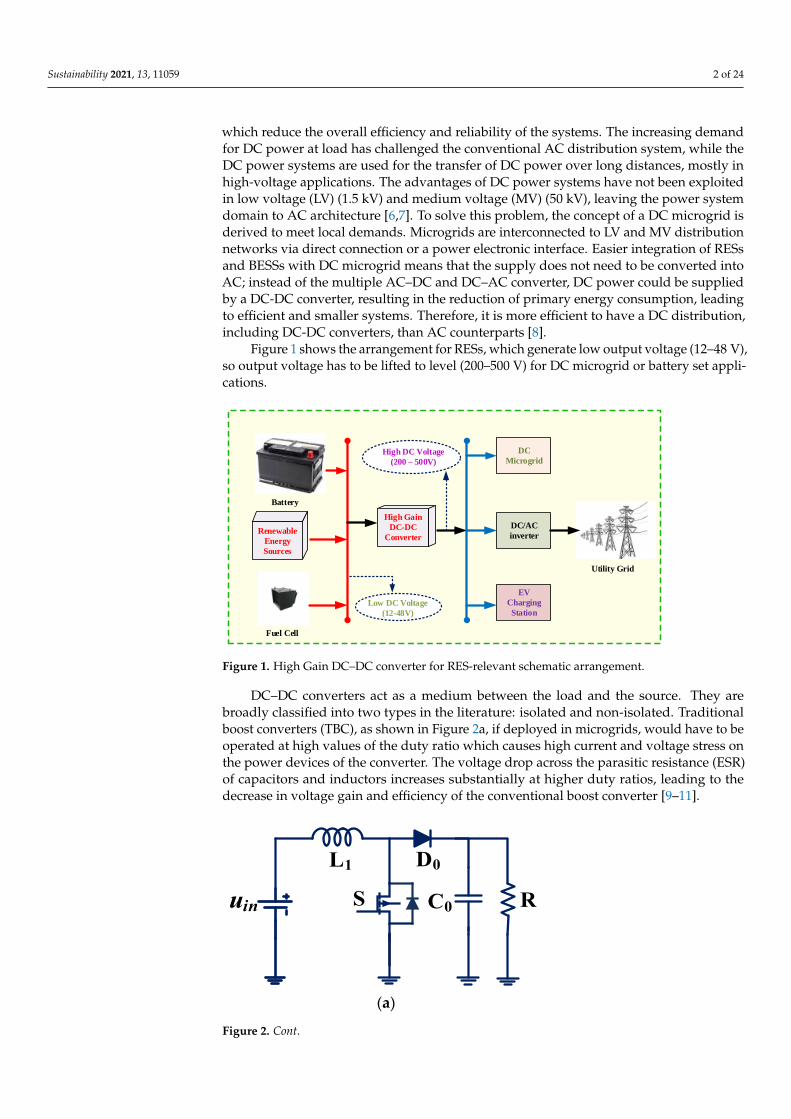
Figure 1 shows the arrangement for RESs, which generate low output voltage (12–48 V),so output voltage has to be lifted to level (200–500 V) for DC microgrid or battery set appli-cations.
Sustainability 2021, 131, 1059 2 of 25
tery-based devices are penetrating the market with a rising curve [6]. These systems re-
quire AC–DC conversion systems, so there are multiple stages of AC–DC conversion,
which reduce the overall efficiency and reliability of the systems. The increasing demand
for DC power at load has challenged the conventional AC distribution system, while the
DC power systems are used for the transfer of DC power over long distances, mostly in
high-voltage applications. The advantages of DC power systems have not been exploited
in low voltage (LV) (1.5 kV) and medium voltage (MV) (50 kV), leaving the power system
domain to AC architecture [6,7]. To solve this problem, the concept of a DC microgrid is
derived to meet local demands. Microgrids are interconnected to LV and MV distribution
networks via direct connection or a power electronic interface. Easier integration of RESs
and BESSs with DC microgrid means that the supply does not need to be converted into
AC; instead of the multiple AC–DC and DC–AC converter, DC power could be supplied
by a DC-DC converter, resulting in the reduction of primary energy consumption, leading
to efficient and smaller systems. Therefore, it is more efficient to have a DC distribution,
including DC-DC converters, than AC counterparts [8].
Figure 1 shows the arrangement for RESs, which generate low output voltage (12 V–
48 V), so output voltage has to be lifted to level (200 V–500 V) for DC microgrid or battery
set applications.
DC
Microgrid
Renewable
Energy
Sources
Battery
Fuel Cell
Low DC Voltage
(12-48V)
High Gain
DC-DC
Converter
High DC Voltage
(200 – 500V)
DC/AC
inverter
EV
Charging
Station
Utility Grid
Figure 1. High Gain DC–DC converter for RES-relevant schematic arrangement.
DC–DC converters act as a medium between the load and the source. They are
broadly classified into two types in the literature: isolated and non-isolated. Traditional
boost converters (TBC), as shown in Figure 2a, if deployed in microgrids, would have to
be operated at high values of the duty ratio which causes high current and voltage stress
on the power devices of the converter. The voltage drop across the parasitic resistance
(ESR) of capacitors and inductors increases substantially at higher duty ratios, leading to
the decrease in voltage gain and efficiency of the conventional boost converter [9–11].
uin
L1
C0 R
D0
S
(a)
Figure 1. High Gain DC–DC converter for RES-relevant schematic arrangement.
DC–DC converters act as a medium between the load and the source. They arebroadly classified into two types in the literature: isolated and non-isolated. Traditionalboost converters (TBC), as shown in Figure 2a, if deployed in microgrids, would have to beoperated at high values of the duty ratio which causes high current and voltage stress onthe power devices of the converter. The voltage drop across the parasitic resistance (ESR)of capacitors and inductors increases substantially at higher duty ratios, leading to thedecrease in voltage gain and efficiency of the conventional boost converter [9–11].
Sustainability 2021, 131, 1059 2 of 25
tery-based devices are penetrating the market with a rising curve [6]. These systems re-quire AC–DC conversion systems, so there are multiple stages of AC–DC conversion, which reduce the overall efficiency and reliability of the systems. The increasing demand for DC power at load has challenged the conventional AC distribution system, while the DC power systems are used for the transfer of DC power over long distances, mostly in high-voltage applications. The advantages of DC power systems have not been exploited in low voltage (LV) (1.5 kV) and medium voltage (MV) (50 kV), leaving the power system domain to AC architecture [6,7]. To solve this problem, the concept of a DC microgrid is derived to meet local demands. Microgrids are interconnected to LV and MV distribution networks via direct connection or a power electronic interface. Easier integration of RESs and BESSs with DC microgrid means that the supply does not need to be converted into AC; instead of the multiple AC–DC and DC–AC converter, DC power could be supplied by a DC-DC converter, resulting in the reduction of primary energy consumption, leading to efficient and smaller systems. Therefore, it is more efficient to have a DC distribution, including DC-DC converters, than AC counterparts [8].
Figure 1 shows the arrangement for RESs, which generate low output voltage (12 V–48 V), so output voltage has to be lifted to level (200 V–500 V) for DC microgrid or battery set applications.
DC Microgrid
Renewable Energy Sources
Battery
Fuel Cell
Low DC Voltage(12-48V)
High Gain DC-DC
Converter
High DC Voltage(200 – 500V)
DC/ACinverter
EV Charging Station
Utility Grid
Figure 1. High Gain DC–DC converter for RES-relevant schematic arrangement.
DC–DC converters act as a medium between the load and the source. They are broadly classified into two types in the literature: isolated and non-isolated. Traditional boost converters (TBC), as shown in Figure 2a, if deployed in microgrids, would have to be operated at high values of the duty ratio which causes high current and voltage stress on the power devices of the converter. The voltage drop across the parasitic resistance (ESR) of capacitors and inductors increases substantially at higher duty ratios, leading to the decrease in voltage gain and efficiency of the conventional boost converter [9–11].
uin
L1
C0 R
D0
S
(a)
Figure 2. Cont.
Sustainability 2021, 13, 11059 3 of 24Sustainability 2021, 131, 1059 3 of 25
uin
L1 D1 L2
C0R
D2
C2
D0
S
(b)
VL-1 VL-2
uin
L1
D1
D2 L2C1
S
D4
C0R
D3
C3
C2
D0
(c)
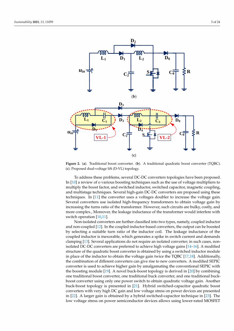
Figure 2. (a). Traditional boost converter. (b). A traditional quadratic boost converter (TQBC). (c). Proposed dual-voltage
lift (D-VL) topology.
To address these problems, several DC-DC converters topologies have been pro-
posed. In [10] a review of o various boosting techniques such as the use of voltage multi-
pliers to multiply the boost factor, and switched inductor, switched capacitor, magnetic
coupling, and multistage techniques. Several high-gain DC-DC converters are proposed
using these techniques. In [11] the converter uses a voltages doubler to increase the volt-
age gain. Several converters use isolated high-frequency transformers to obtain voltage
gain by increasing the turns ratio of the transformer. However, such circuits are bulky,
costly, and more complex., Moreover, the leakage inductance of the transformer would
interfere with switch operation [10,11].
Non-isolated converters are further classified into two types, namely, coupled induc-
tor and non-coupled [12]. In the coupled-inductor-based converters, the output can be
boosted by selecting a suitable turn ratio of the inductor coil. The leakage inductance of
the coupled inductor is inexorable, which generates a spike in switch current and de-
mands clamping [13]. Several applications do not require an isolated converter; in such
cases, non-isolated DC-DC converters are preferred to achieve high voltage gains [14–16].
A modified structure of the quadratic boost converter is obtained by using a switched
inductor module in place of the inductor to obtain the voltage gain twice the TQBC [17,18].
Additionally, the combination of different converters can give rise to new converters. A
modified SEPIC converter is used to achieve higher gain by amalgamating the conven-
tional SEPIC with the boosting module [19]. A novel buck-boost topology is derived in
[20] by combining one traditional boost converter, one traditional buck converter, and one
traditional buck-boost converter using only one power switch to obtain quadratic voltage
gain. Another buck-boost topology is presented in [21]. Hybrid switched-capacitor quad-
ratic boost converters with very high DC gain and low voltage stress on power devices
are presented in [22]. A larger gain is obtained by a hybrid switched-capacitor technique
in [23]. The low voltage stress on power semiconductor devices allows using lower-rated
Figure 2. (a). Traditional boost converter. (b). A traditional quadratic boost converter (TQBC).(c). Proposed dual-voltage lift (D-VL) topology.
To address these problems, several DC-DC converters topologies have been proposed.In [10] a review of o various boosting techniques such as the use of voltage multipliers tomultiply the boost factor, and switched inductor, switched capacitor, magnetic coupling,and multistage techniques. Several high-gain DC-DC converters are proposed using thesetechniques. In [11] the converter uses a voltages doubler to increase the voltage gain.Several converters use isolated high-frequency transformers to obtain voltage gain byincreasing the turns ratio of the transformer. However, such circuits are bulky, costly, andmore complex., Moreover, the leakage inductance of the transformer would interfere withswitch operation [10,11].
Non-isolated converters are further classified into two types, namely, coupled inductorand non-coupled [12]. In the coupled-inductor-based converters, the output can be boostedby selecting a suitable turn ratio of the inductor coil. The leakage inductance of thecoupled inductor is inexorable, which generates a spike in switch current and demandsclamping [13]. Several applications do not require an isolated converter; in such cases, non-isolated DC-DC converters are preferred to achieve high voltage gains [14–16]. A modifiedstructure of the quadratic boost converter is obtained by using a switched inductor modulein place of the inductor to obtain the voltage gain twice the TQBC [17,18]. Additionally,the combination of different converters can give rise to new converters. A modified SEPICconverter is used to achieve higher gain by amalgamating the conventional SEPIC withthe boosting module [19]. A novel buck-boost topology is derived in [20] by combiningone traditional boost converter, one traditional buck converter, and one traditional buck-boost converter using only one power switch to obtain quadratic voltage gain. Anotherbuck-boost topology is presented in [21]. Hybrid switched-capacitor quadratic boostconverters with very high DC gain and low voltage stress on power devices are presentedin [22]. A larger gain is obtained by a hybrid switched-capacitor technique in [23]. Thelow voltage stress on power semiconductor devices allows using lower-rated MOSFET
Sustainability 2021, 13, 11059 4 of 24
with low on-resistance to obtain better efficiency by reducing conduction and switchingloss [23].
The voltage lift (VL) technique is a well-known method widely used in electroniccircuit design. In recent years, it has been successfully used in DC-DC converter appli-cations and paved the way for the design of high voltage gain converters. The use ofthe VL technique was confirmed by Luo by developing DC-DC converters [24]. It usesextra energy storage elements inductors and capacitors to enhance the voltage gain of thecircuit. Luo proposed a series of positive output Luo converters, such as a self-lift circuit,re-lift circuit, triple-lift, and quadruple-lift boost converters. This technique was used toovercome the effects of the parasitic elements and to boost the voltage at the output. In [25]a high-gain converter using the VL technique to achieve gain equal to twice the traditionalboost converter using two inductors, but this converter has switch stress equal to the outputvoltage. A voltage doubler circuit such as Cockroft–Walton can be used to increase theoutput voltage [26], and it reduces the voltage stress across the switch. Additionally, the VLtechnique is used in [25–28] with a voltage doubler. A non-isolated DC-DC converter basedon the VL technique was used to obtain a negative voltage concerning the ground [29]. Theisolated category of converter bases on interleaving technique is proposed in ref. [30]
In this paper, the proposed non-isolated quadratic boost converter utilizes the dualvoltage lift (VL) technique to increase the gain of the converter. The proposed topology hasthe following advantages.
1. The voltage gain is greater than TBC and QBC.2. The voltage stress on the power switch is lower than the output voltage.3. The voltage doubler is avoided to increase the voltage gain.4. A single power switch that makes control easy reduces gate drive requirements.5. The low voltage stress on power devices reduces the power losses, hence the converter
efficiency is increased.6. A common ground connection is available between the source and load.
2. Operating Principle of the D-VL Converter
The proposed schematic illuminated in Figure 2c uses two voltage lift cells. Thecombination of L1, C1, and D1 is the first voltage lift cell (VL-1), whereas the similarcombination of L2, C2, and D2 is (VL-2). The proposed converter has two inductors, fourcapacitors, and five diodes. The converter utilizes a single power switch, so the controlis very easy. Taking a single voltage lift cell (VL-1), when Switch S is ON, the additionalcapacitor C1 is connected in parallel with Inductor L1 and charged by an input DC source.When the switch is OFF, the energy storage capacitor C1 is connected in series with DCinput, and Inductor L1 discharges energy to pure resistive load R. Same situation occurs inVL-2. This way, voltage gain improvement is achieved and reduced switch stress over atraditional quadratic boost converter (TQBC), as depicted in Figure 2b.
2.1. Continuous Conduction Mode (CCM) of the D-VL Converter
The continuous conduction mode of the D-VL converter can be analyzed in two modesof operation.
Mode 1 (t1 < t < t0): The equivalent circuit related to this mode is shown in Figure 3a.inductor L1 is charged by input source Uin through D3 and S. Moreover, inductor L2is charge by capacitors C1 and C2 through S. In this interval, inductor currents have apositive slope and store energy. The output DC load is fed by output capacitor voltage UC0.Waveform’s profile of the proposed converter is shown in Figure 4. The governing voltageequations are as follows
L1diL1dt = uL1 = uin
L2diL2dt = uL2 = uC3
uC1 = uC3 − uC2 + uinuC2 = uC3uC1 = uin
(1)
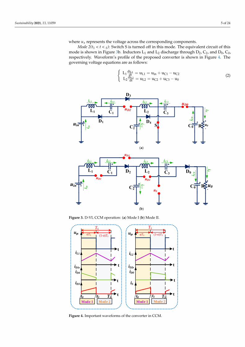
Sustainability 2021, 13, 11059 5 of 24
where ux represents the voltage across the corresponding components.Mode 2(t1 < t < S): Switch S is turned off in this mode. The equivalent circuit of this
mode is shown in Figure 3b. Inductors L1 and L2 discharge through D2, C2, and D0, C0,respectively. Waveform’s profile of the proposed converter is shown in Figure 4. Thegoverning voltage equations are as follows:
L1diL1dt = uL1 = uin + uC1 − uC2
L2diL2dt = uL2 = uC2 + uC3 − u0
(2)
Sustainability 2021, 131, 1059 5 of 25
⎩⎪⎪⎨⎪⎪⎧ L didt = u = uL didt = u = u u = u − u +uu = uu = u
(1)
where 𝑢 represents the voltage across the corresponding components. Mode 2(t1 < t < S): Switch S is turned off in this mode. The equivalent circuit of this
mode is shown in Figure 3b. Inductors L1 and L2 discharge through D2, C2, and D0, C0, respectively. Waveform’s profile of the proposed converter is shown in Figure 4. The gov-erning voltage equations are as follows: L didt = u = u + u − uL didt = u = u + u − u (2)
uin
L1
D1
uD2 L2C1
SD4
C0 R
D3
C3
C2
uD0iL1 iL2
+
+
+
+ +
-u0
i0
i C0
iC1 iC3iC2
i in
(a)
uin
L1 D2 L2C1
C0 R
C3
C2
D0uD1
uD3
uD4
uS
+
++
++
-u0i in
iL1 iC1 iL2 iC3
iC2
i C0
i0
(b)
Figure 3. D-VL CCM operation: (a) Mode I (b) Mode II. Figure 3. D-VL CCM operation: (a) Mode I (b) Mode II.
Sustainability 2021, 131, 1059 6 of 25
TS
aTS (1-a)TS
iL1
iD1,
iD4
ugs
iL2
ugs
iS
iD2,
iD0
iD3
aTS (1-a)TS
TS
t
t
t
t
t
t
t
tt0 t1 TS t0 t1 TS
Mode 1 Mode 2 Mode 1 Mode 2
Figure 4. Important waveforms of the converter in CCM.
Voltage Gain Calculation
During steady-state conditions, the average voltage across an inductor is zero, i.e.,
∫ 𝑢𝐿𝑑𝑡 = 0𝑇𝑠0
Using the derived voltage Equations (1) and (2), we can extract the volt-second bal-
ance equations as
uinα + (uin + uC1 − uC2)(1 − α) = 0uC3α + (uC2 + uC3 − u0)(1 − α) = 0
(3)
where α is the duty ratio.
Using Equations (1)–(3), the following results are obtained:
uC3 = (
2 − α
1 − α)uin
uC3 = (1 − α
2 − α)u0
(4)
Using (4) voltage gain Kccm for the proposed converter, the results are:
Kccm = u0uin
= (2 − α
1 − α)2
(5)
2.2. Mismatch Operating Modes of the Inductors of the proposed D VL Converter
The converter enters the DCM mode of operation when the inductor current goes to
zero at any time of interval. Consider two cases of operation:
2.2.1. Case I: Inductor L1 operating in DCM and L2 into CCM
Inductor L1 is sufficiently high so that ripple is neglected. A low value of inductance
of L2 makes the ripple high in inductor current L2, and the current goes to zero before the
time interval TS. The waveform of the considered operation is shown in Figure 5a.
Figure 4. Important waveforms of the converter in CCM.
Sustainability 2021, 13, 11059 6 of 24
Voltage Gain Calculation
During steady-state conditions, the average voltage across an inductor is zero, i.e.,∫ Ts0 uLdt = 0.
Using the derived voltage Equations (1) and (2), we can extract the volt-second balanceequations as
uinα+ (uin + uC1 − uC2)(1− α) = 0uC3α+ (uC2 + uC3 − u0)(1− α) = 0
(3)
where α is the duty ratio.Using Equations (1)–(3), the following results are obtained:
uC3 =( 2−α
1−α)uin
uC3 =(
1−α2−α
)u0
(4)
Using (4) voltage gain Kccm for the proposed converter, the results are:
Kccm =u0
uin=
(2− α
1− α
)2(5)
2.2. Mismatch Operating Modes of the Inductors of the Proposed D VL Converter
The converter enters the DCM mode of operation when the inductor current goes tozero at any time of interval. Consider two cases of operation:
2.2.1. Case I: Inductor L1 Operating in DCM and L2 into CCM
Inductor L1 is sufficiently high so that ripple is neglected. A low value of inductanceof L2 makes the ripple high in inductor current L2, and the current goes to zero before thetime interval TS. The waveform of the considered operation is shown in Figure 5a.
Sustainability 2021, 131, 1059 7 of 25
aTS a1TS
iL1,
iL2
iD2
ugs
t
t
tt0 t1 TS
1 2
ipkL1
3
aTS a1TS
iL1,
iL2
iD0
ugs
t
t
tt0 t1 TS
1 2 3
t2 t2
CASE I: DCM CASE II: DCM
(a) (b)
ipkL2
Figure 5. DCM waveforms (a) Case I: Inductor L1 operating in DCM and L2 into CCM (b) Case II:
Inductor L2 operating in DCM and L1 into CCM.
Mode 1(t0 < t < t1):
The power switch is ON for this duration. Inductor L1 starts to magnetize from zero
and reaches the maximum at the end at time DTS. This mode is the same as CCM Mode I.
The governing relations in this mode is given by Equation (1)
Mode 2(t1 < t < t2):
The power switch is OFF in this time interval. Inductor L1 starts to demagnetize, and
the current falls to null at the end of the interval α1Ts. The governing relations in this in-
terval are given by (2).
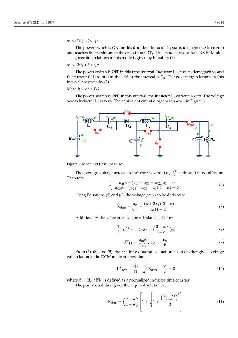
Mode 3(t2 < t < TS):
The power switch is OFF. In this interval, the Inductor L1 current is zero. The voltage
across Inductor L1 is zero. The equivalent circuit diagram is shown in Figure 6.
uin
L1 D2 L2C1
C0 R
C3
C2
uD0
uD1
uD3
uD4
uS
+
++
++
-u0i in
iL1=0 iC1 iL2 iC3
iC2
i C0
i0
Figure 6. Mode 3 of Case I of DCM.
The average voltage across an inductor is zero, i.e., ∫ uLdt = 0Ts0
in equilibrium.
Therefore,
uinα + (uin + uC1 − uC2)α1 = 0
uC3α + (uC2 + uC3 − u0)(1 − α) = 0 (6)
Figure 5. DCM waveforms (a) Case I: Inductor L1 operating in DCM and L2 into CCM (b) Case II:Inductor L2 operating in DCM and L1 into CCM.
Sustainability 2021, 13, 11059 7 of 24
Mode 1(t0 < t < t1):
The power switch is ON for this duration. Inductor L1 starts to magnetize from zeroand reaches the maximum at the end at time DTS. This mode is the same as CCM Mode I.The governing relations in this mode is given by Equation (1).
Mode 2(t1 < t < t2):
The power switch is OFF in this time interval. Inductor L1 starts to demagnetize, andthe current falls to null at the end of the interval α1Ts. The governing relations in thisinterval are given by (2).
Mode 3(t2 < t < TS):
The power switch is OFF. In this interval, the Inductor L1 current is zero. The voltageacross Inductor L1 is zero. The equivalent circuit diagram is shown in Figure 6.
Sustainability 2021, 131, 1059 7 of 25
aTS a1TS
iL1,iL2
iD2
ugs
t
t
tt0 t1 TS
1 2
ipkL1
3
aTS a1TS
iL1,iL2
iD0
ugs
t
t
tt0 t1 TS
1 2 3
t2 t2
CASE I: DCM CASE II: DCM
(a) (b)
ipkL2
Figure 5. DCM waveforms (a) Case I: Inductor L1 operating in DCM and L2 into CCM (b) Case II: Inductor L2 operating in DCM and L1 into CCM.
Mode 1(t0 < t < t1): The power switch is ON for this duration. Inductor L1 starts to magnetize from zero
and reaches the maximum at the end at time DTS. This mode is the same as CCM Mode I. The governing relations in this mode is given by Equation (1)
Mode 2(t1 < t < t2): The power switch is OFF in this time interval. Inductor L1 starts to demagnetize, and
the current falls to null at the end of the interval α1Ts. The governing relations in this in-terval are given by (2). Mode 3(t2 < t < TS):
The power switch is OFF. In this interval, the Inductor L1 current is zero. The voltage across Inductor L1 is zero. The equivalent circuit diagram is shown in Figure 6.
uin
L1 D2 L2C1
C0 R
C3
C2
uD0
uD1
uD3
uD4
uS
+
++
++
-u0i in
iL1=0 iC1 iL2 iC3
iC2
i C0
i0
Figure 6. Mode 3 of Case I of DCM.
The average voltage across an inductor is zero, i.e., u dt = 0 in equilibrium. Therefore, u α + (u + u − u )α = 0u α + (u + u − u )(1 − α) = 0 (6)
Figure 6. Mode 3 of Case I of DCM.
The average voltage across an inductor is zero, i.e.,∫ Ts
0 uLdt = 0 in equilibrium.Therefore,
uinα+ (uin + uC1 − uC2)α1 = 0uC3α+ (uC2 + uC3 − u0)(1− α) = 0
(6)
Using Equations (4) and (6), the voltage gain can be derived as
Kdcm =u0
uin=
(α+ 2α1)(2− α)
α1(1− α)(7)
Additionally, the value of α1 can be calculated as below:
12α1ipk
L1 = 〈iD2〉 =(
2− α
1− α
)〈i0〉 (8)
ipkL1 =
uinα
L1fs; 〈i0〉 =
u0
R(9)
From (7), (8), and (9), the resulting quadratic equation has roots that give a voltagegain relation in the DCM mode of operation.
K2dcm −
2(2− α)
(1− α)Kdcm −
α2
β= 0 (10)
where β = 2L1/RTS is defined as a normalized inductor time constant.The positive solution gives the required solution, i.e.,
Kdcm =
(2− α
1− α
)1 +
√√√√1 +
(α(1−α)
2−α
)2
β
(11)
Sustainability 2021, 13, 11059 8 of 24
Boundary Condition Mode:
In Mode 2, the inductor current of L1 becomes zero at the end of αTS. This mode istermed a boundary condition mode (BCM). In this mode, the voltage gain of CCM modeand DCM mode are equal, i.e.,
Kdcm = Kccm =
(2− α
1− α
)2=
(2− α
1− α
)1 +
√√√√1 +
(α(1−α)
2−α
)2
β
(12)
The following relation is yielded from (12):
β = βL1 BCM =α(1− α)4
(2− α)3 (13)
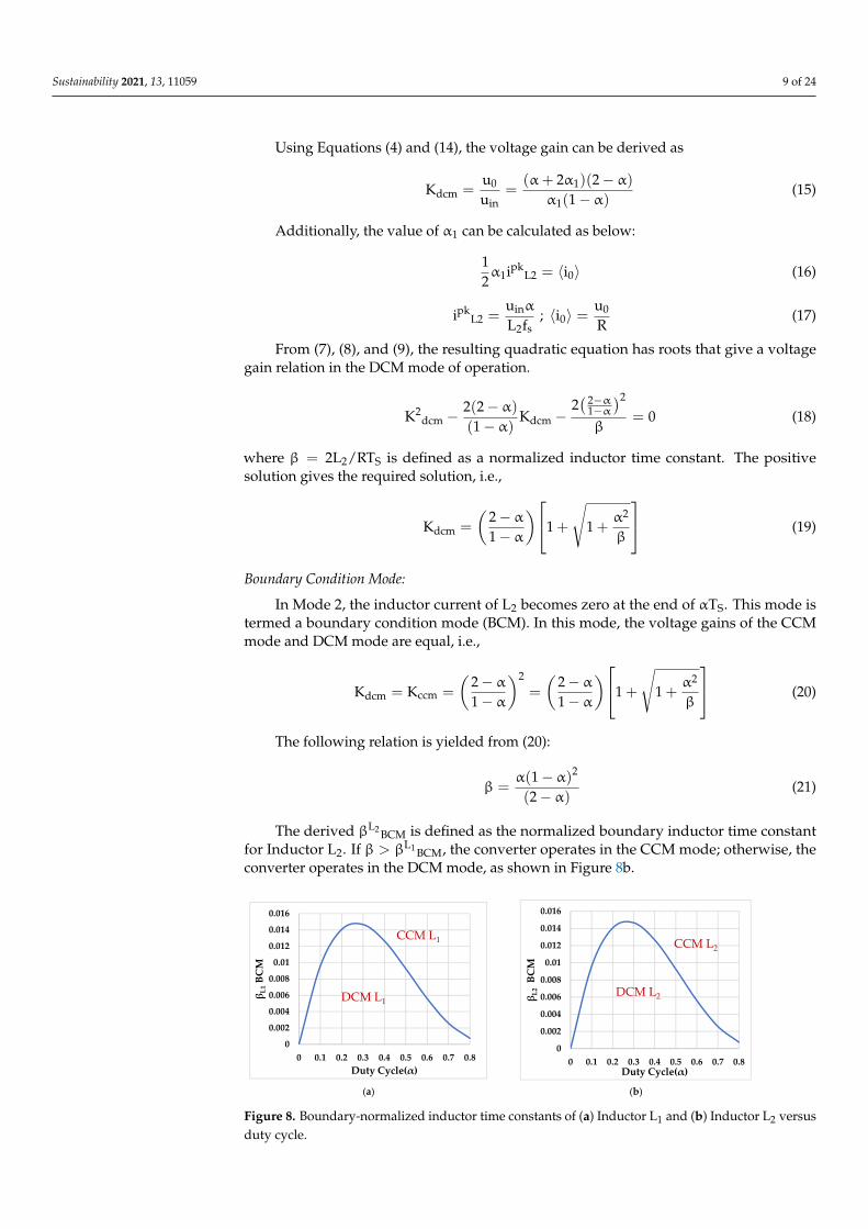
The derived βL1 BCM is defined as the normalized boundary inductor time constant forInductor L1. If β > βL1 BCM, the converter operates in CCM mode; otherwise, the converteroperates in DCM mode, as shown in Figure 8a.
2.2.2. Case II: Inductor L2 Operating in DCM and L1 into CCM
Inductor L2 is sufficiently high so that ripple is neglected. A low value of inductanceof L1 makes ripple high in inductor current L1, and the current goes to zero before the timeinterval TS. The waveform of the considered operation is shown in Figure 5b.
Mode 1(t0 < t < t1):
The power switch is ON for this duration. Inductor L1 starts to magnetize from zerovalue and reach the maximum at the end at time DTS. This mode is the same as CCMMode I. The governing relations in this mode are given by Equation (1):
Mode 2(t1 < t < t2):
The power switch is OFF in this time interval. Inductor L2 starts to demagnetize, andthe current falls to zero at the end of the interval α1Ts. The governing relations in thisinterval are given by Equation (2).
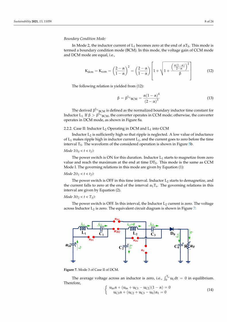
Mode 3(t2 < t < TS):
The power switch is OFF. In this interval, the Inductor L2 current is zero. The voltageacross Inductor L2 is zero. The equivalent circuit diagram is shown in Figure 7:
Sustainability 2021, 131, 1059 9 of 25
Mode 3(t2 < t < TS): The power switch is OFF. In this interval, the Inductor L2 current is zero. The voltage
across Inductor L2 is zero. The equivalent circuit diagram is shown in Figure 7:
uin
L1uD2 L2C1
C0 R
C3
C2
D0uD1
uD3
uD4
uS
+
++
++
-u0i in
iL1 iC1 iL2=0 iC3
iC2
i C0
i0
Figure 7. Mode 3 of Case II of DCM.
The average voltage across an inductor is zero, i.e., u dt = 0 in equilibrium. Therefore, u α + (u + u − u )(1 − α) = 0u α + (u + u − u )α = 0 (14)
Using Equations (4) and (14), the voltage gain can be derived as K = uu = (α + 2α1)(2 − α)α1(1 − α) (15)
Additionally, the value of α1 can be calculated as below: 12 α i = ⟨i ⟩ (16)
i = ; ⟨i ⟩ = (17)
From (7), (8), and (9), the resulting quadratic equation has roots that give a voltage gain relation in the DCM mode of operation.
K − 2(2 − α)(1 − α) K − 2 2 − α1 − αβ = 0 (18)
where β = 2L RT⁄ is defined as a normalized inductor time constant. The positive solu-tion gives the required solution, i.e.,
K = 2 − α1 − α 1 + 1 + αβ (29)
Boundary Condition Mode: In Mode 2, the inductor current of L2 becomes zero at the end of αTS. This mode is
termed a boundary condition mode (BCM). In this mode, the voltage gains of the CCM mode and DCM mode are equal, i.e.,
K = Kccm = 2 − α1 − α = 2 − α1 − α 1 + 1 + αβ (20)
The following relation is yielded from (20):
Figure 7. Mode 3 of Case II of DCM.
The average voltage across an inductor is zero, i.e.,∫ Ts
0 uLdt = 0 in equilibrium.Therefore,
uinα+ (uin + uC1 − uC2)(1− α) = 0uC3α+ (uC2 + uC3 − u0)α1 = 0
(14)
Sustainability 2021, 13, 11059 9 of 24
Using Equations (4) and (14), the voltage gain can be derived as
Kdcm =u0
uin=
(α+ 2α1)(2− α)
α1(1− α)(15)
Additionally, the value of α1 can be calculated as below:
12α1ipk
L2 = 〈i0〉 (16)
ipkL2 =
uinα
L2fs; 〈i0〉 =
u0
R(17)
From (7), (8), and (9), the resulting quadratic equation has roots that give a voltagegain relation in the DCM mode of operation.
K2dcm −
2(2− α)
(1− α)Kdcm −
2( 2−α
1−α)2
β= 0 (18)
where β = 2L2/RTS is defined as a normalized inductor time constant. The positivesolution gives the required solution, i.e.,
Kdcm =
(2− α
1− α
)1 +
√1 +
α2
β
(19)
Boundary Condition Mode:
In Mode 2, the inductor current of L2 becomes zero at the end of αTS. This mode istermed a boundary condition mode (BCM). In this mode, the voltage gains of the CCMmode and DCM mode are equal, i.e.,
Kdcm = Kccm =
(2− α
1− α
)2=
(2− α
1− α
)1 +
√1 +
α2
β
(20)
The following relation is yielded from (20):
β =α(1− α)2
(2− α)(21)
The derived βL2 BCM is defined as the normalized boundary inductor time constantfor Inductor L2. If β > βL1 BCM, the converter operates in the CCM mode; otherwise, theconverter operates in the DCM mode, as shown in Figure 8b.
Sustainability 2021, 131, 1059 10 of 25
β = α(1 − α)(2 − α) (21)
The derived β is defined as the normalized boundary inductor time constant for Inductor L2. If β > β , the converter operates in the CCM mode; otherwise, the converter operates in the DCM mode, as shown in Figure 8b.
(a) (b)
Figure 8. Boundary-normalized inductor time constants of (a) Inductor L1 and (b) Inductor L2 versus duty cycle.
2.3. Effect of ESR of Inductor on Voltage Gain Parasitic resistance ESR r is considered. Inductor L in Figure 2 is replaced by this
arrangement, as shown in Figure 9. The voltage across Inductor L can be determined in both modes as follows:
Switch-ON mode⇒ u = u − i r u = u − i r (22)
Switch-OFF mode⇒ u = u + u − u − i r u = u + u − u − i r (23)
The average value of voltage across the inductor is zero. Therefore, the following expressions are derived:
⎩⎪⎨⎪⎧u = (2 − α)u − i r(1 − α)u = (2 − α)u − i r(1 − α) (24)
Therefore, the effect of ESR on voltage gain can be calculated using (24): VV , = (2 − α 1 − α⁄ )1 + (2 − α)(1 − α) rR + (2 − α)(1 − α) rR (25)
If r = r = r , then VV = (2 − α 1 − α⁄ )1 + (2 − α)(3 − 3α + α )(1 − α) rR (26)
The effect of ESR of inductors on voltage is shown in Figure 10.
0
0.002
0.004
0.006
0.008
0.01
0.012
0.014
0.016
0 0.1 0.2 0.3 0.4 0.5 0.6 0.7 0.8
β L1
BCM
Duty Cycle(α)
DCM L1
CCM L1
0
0.002
0.004
0.006
0.008
0.01
0.012
0.014
0.016
0 0.1 0.2 0.3 0.4 0.5 0.6 0.7 0.8
β L2
BCM
Duty Cycle(α)
CCM L2
DCM L2
Figure 8. Boundary-normalized inductor time constants of (a) Inductor L1 and (b) Inductor L2 versusduty cycle.
Sustainability 2021, 13, 11059 10 of 24
2.3. Effect of ESR of Inductor on Voltage Gain
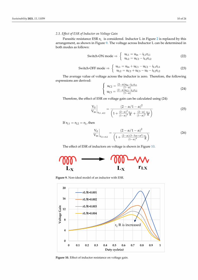
Parasitic resistance ESR rL is considered. Inductor L in Figure 2 is replaced by thisarrangement, as shown in Figure 9. The voltage across Inductor L can be determined inboth modes as follows:
Switch-ON mode⇒
uL1 = uin − iL1rL1uL2 = uC2 − iL2rL2
(22)
Switch-OFF mode⇒
uL1 = uin + uC1 − uC2 − iL1rL1uL2 = uC2 + uC3 − u0 − iL2rL2
(23)
The average value of voltage across the inductor is zero. Therefore, the followingexpressions are derived: uC2 = (2−α)uin−iL1rL1
(1−α)
uC3 = (2−α)uC2−iL2rL2(1−α)
(24)
Therefore, the effect of ESR on voltage gain can be calculated using (24):
V0
Vin
∣∣∣∣rL1 ,rL2
=(2− α/1− α)2(
1 + (2−α)2
(1−α)4rL1R + (2−α)
(1−α)2rL2R
) (25)
If rL1 = rL2 = rL, then
V0
Vin
∣∣∣∣rL1=rL2
=(2− α/1− α)2(
1 + (2−α)(3−3α+α2)
(1−α)4rLR
) (26)
The effect of ESR of inductors on voltage is shown in Figure 10.Sustainability 2021, 131, 1059 11 of 25
LX rLXLX Figure 9. Non-ideal model of an inductor with ESR.
Figure 10. Effect of inductor resistance on voltage gain.
2.4. Current Stress of Components If the converter is assumed loss-free, then
⎩⎪⎨⎪⎧ P = Pu ⟨i ⟩ = u ⟨i ⟩⟨i ⟩⟨i ⟩ = uu = K = 2 − α1 − α (27)
where ⟨i ⟩ is the average current of any element of the proposed converter. According to the modes of operation of the proposed converter, i , i are the capacitor currents when S is turned ON and i , i are the capacitor currents when S is turned OFF. The current expressions are shown in (28).
⎩⎪⎨⎪⎧ i = i − ii = −⟨i ⟩i = ii = i − ⟨i ⟩ (28)
Applying current–second balance on capacitor C1 and C0: i α + i (1 − α) = 0 (29)i α + i (1 − α) = 0 (30)
Using Equations (28)–(30), the average inductor currents ⟨i ⟩ and ⟨i ⟩ can be drawn out as ⟨iL1⟩ = 2 − α(1 − α)2 ⟨i0⟩⟨iL2⟩ = 11 − α ⟨i0⟩ (31)
0
4
8
12
16
20
0 0.1 0.2 0.3 0.4 0.5 0.6 0.7 0.8 0.9 1
Vol
tage
Gai
n
Duty cycle(α)
rL/R=0.001
rL/R=0.002
rL/R=0.003
rL/R=0.004
rL/R is increased
Figure 9. Non-ideal model of an inductor with ESR.
Sustainability 2021, 131, 1059 11 of 25
LX rLXLX Figure 9. Non-ideal model of an inductor with ESR.
Figure 10. Effect of inductor resistance on voltage gain.
2.4. Current Stress of Components If the converter is assumed loss-free, then
⎩⎪⎨⎪⎧ P = Pu ⟨i ⟩ = u ⟨i ⟩⟨i ⟩⟨i ⟩ = uu = K = 2 − α1 − α (27)
where ⟨i ⟩ is the average current of any element of the proposed converter. According to the modes of operation of the proposed converter, i , i are the capacitor currents when S is turned ON and i , i are the capacitor currents when S is turned OFF. The current expressions are shown in (28).
⎩⎪⎨⎪⎧ i = i − ii = −⟨i ⟩i = ii = i − ⟨i ⟩ (28)
Applying current–second balance on capacitor C1 and C0: i α + i (1 − α) = 0 (29)i α + i (1 − α) = 0 (30)
Using Equations (28)–(30), the average inductor currents ⟨i ⟩ and ⟨i ⟩ can be drawn out as ⟨iL1⟩ = 2 − α(1 − α)2 ⟨i0⟩⟨iL2⟩ = 11 − α ⟨i0⟩ (31)
0
4
8
12
16
20
0 0.1 0.2 0.3 0.4 0.5 0.6 0.7 0.8 0.9 1
Vol
tage
Gai
n
Duty cycle(α)
rL/R=0.001
rL/R=0.002
rL/R=0.003
rL/R=0.004
rL/R is increased
Figure 10. Effect of inductor resistance on voltage gain.
Sustainability 2021, 13, 11059 11 of 24
2.4. Current Stress of Components
If the converter is assumed loss-free, thenPin = Pout
uin〈iin〉 = u0〈i0〉〈iin〉〈i0〉
= u0uin
= Kccm =( 2−α
1−α)2
(27)
where 〈ix〉 is the average current of any element of the proposed converter. According tothe modes of operation of the proposed converter, iC1on , iC0on are the capacitor currentswhen S is turned ON and iC1off , iC0off are the capacitor currents when S is turned OFF. Thecurrent expressions are shown in (28).
iC1on = iL1 − iD3iC0on = −〈i0〉
iC1off = iL1iC0off = iL2 − 〈i0〉
(28)
Applying current–second balance on capacitor C1 and C0:
iC1onα+ iC1off(1− α) = 0 (29)
iC0onα+ iC0off(1− α) = 0 (30)
Using Equations (28)–(30), the average inductor currents 〈iL1〉 and 〈iL2〉 can be drawnout as 〈iL1〉 =
(2−α
(1−α)2
)〈i0〉
〈iL2〉 =(
11−α
)〈i0〉
(31)
Likewise, applying current–second balance on capacitor C2 and C3, the averagecurrent through power diodes (D0 to D4) and power Switch (S) can be obtained as
〈iD1〉 = 〈iD2〉 =( 2−α
1−α)〈i0〉
〈iD3〉 =(
2−α(1−α)2
)〈i0〉, 〈iD4〉 = 〈iD0〉 = 〈i0〉
〈iS〉 =(
3−2α(1−α)2
)〈i0〉
(32)
3. Design of Circuit Components
Inductors are designed based on current ripple, and capacitors are designed based onvoltage ripple.
(A) Inductor Design:Using Equation (1), the value of inductors L1 and L2 can be extracted as follows:
L1 = uinα∆iL1fs
L2 = uin(2−α)α(1−α)∆iL2fs
(33)
where ∆iL1 and ∆iL2 are the ripples in inductor currents L1 and L2, and fs is the switchingfrequency.
(B) Capacitor Design:The capacitor value depends upon its charging current, the voltage ripple ∆uCx across
it, duty ratio, and switching frequency fs.Using Equation (7), we can obtain the value of C0 and C1 as follows:
C0 =α〈i0〉
∆uC0fs, C1 =
(2− α)〈i0〉(1− α)∆uC1fs
(34)
Sustainability 2021, 13, 11059 12 of 24
Likewise, the rest capacitor value can be drawn out as
C2 =〈i0〉
(1− α)∆uC2fs, C3 =
〈i0〉∆uC3fs
(35)
where ∆uCx is the voltage ripple in capacitor voltage.(C) Selection of Diodes and Switch:The voltage across power diodes (D0 to D4) and the power Switch (S) are as follows:
uD0 =
(
2−α(1−α)2
)uin, 0 < t < αTs
0 , 0 < t < αTs
, (36)
uD1 =
0, 0 < t < αTs(
11−α
)uin, 0 < t < αTs
(37)
uD2 =
(1
1−α
)uin, 0 < t < αTs
0 , 0 < t < αTs, (38)
uD3 =
0, 0 < t < αTs(1
(1−α)2
)uin, 0 < t < αTs
(39)
uD4 =
0, 0 < t < αTs(2−α
(1−α)2
)uin, 0 < t < αTs
(40)
uS =
0, 0 < t < αTs(2−α
(1−α)2
)uin, 0 < t < αTs
(41)
where Ts is the switching period.
4. Power Loss Calculation in the Proposed Dual VL Converter
The equivalent circuit, including parasitic resistors, is also considered to analyze theproposed converter circuit. In a non-ideal equivalent circuit, all components are replacedwith their parasitic resistances, as shown in Figure 11, where rS is the switch on-resistance,rD is the diode on-resistance, and uF is the diode’s threshold voltage. The ESR of theinductor is taken as rL. The ESR of the capacitor is taken as rC. Assuming that the inductorcurrent has no ripple. The power output is given as
P0 = u0i0 = 〈i0〉2R
Sustainability 2021, 131, 1059 13 of 25
u = 0, 0 < t < αT2 − α(1 − α) u , 0 < t < αT (40)
u = 0, 0 < t < αT2 − α(1 − α) u , 0 < t < αT (41)
where Ts is the switching period.
4. Power Loss Calculation in the proposed Dual VL Converter The equivalent circuit, including parasitic resistors, is also considered to analyze the
proposed converter circuit. In a non-ideal equivalent circuit, all components are replaced with their parasitic resistances, as shown in Figure 11, where rS is the switch on-resistance, rD is the diode on-resistance, and uF is the diode’s threshold voltage. The ESR of the in-ductor is taken as rL. The ESR of the capacitor is taken as rC. Assuming that the inductor current has no ripple. The power output is given as P = u ⟨i ⟩ = ⟨i ⟩ R
L L rLr D
S Sr S
VDD
C C rC
Figure 11. Equivalent non-ideal model of components.
(a) Switch Losses The root mean square value of the current passing through the switch is i , and P and P are the switching loss and conduction loss of switch S.
⎩⎪⎪⎨⎪⎪⎧ i = 3 − 2α(1 − α) √α ⟨i ⟩
P = i r = (3 − 2α)(1 − α) α ⟨i ⟩ r = (3 − 2α)(1 − α) α rR PP = 12T (⟨i ⟩u ) (t + t ) (42)
where the rising and falling times of S are given by t and t , respectively. Total loss by the switch is calculated as P = P + P (43)
(b) Power losses in diodes The root mean square current of the diode is notified by i . The power loss due
to ON resistance of diodes is P and P is the loss due to forward voltage drop u of the diodes. Diode loss is calculated as P = u ⟨i ⟩ + i r (44)
Figure 11. Equivalent non-ideal model of components.
(a) Switch Losses
Sustainability 2021, 13, 11059 13 of 24
The root mean square value of the current passing through the switch is iSrms , andPSSW and PScon are the switching loss and conduction loss of switch S.
iSrms =
(3−2α
(1−α)2√α
)〈i0〉
PScon = iSrms2rS =
((3−2α)2
(1−α)4α
)〈i0〉2 rS =
((3−2α)2
(1−α)4α
)rSR P0
PSSW = 12TS
(〈is〉uS) (tr + tf )
(42)
where the rising and falling times of S are given by tr and tf, respectively. Total loss by theswitch is calculated as
PStotal = PScon + PSSW (43)
(b) Power losses in diodesThe root mean square current of the diode is notified by iDxrms . The power loss due to
ON resistance of diodes is PrDx and PuFx is the loss due to forward voltage drop uFx of thediodes. Diode loss is calculated as
PDx = uFx〈iDx〉+ iDxrms2rDx (44)
iD1rms =(2−α)〈i0〉(1−α)
√α
PD1 =( 2−α
1−α)uF1〈i0〉+
((2−α)2
α(1−α)2
)〈i0〉2rD1 =
( 2−α1−α
)uF1u0
P0 +
((2−α)2
α(1−α)2
)rD1R P0
iD2rms =(2−α)〈i0〉√
(1−α)3
PD2 =(
2−α(1−α)
)uF2〈i0〉+
((2−α)2
(1−α)3
)〈i0〉2rD2 =
( 2−α1−α
)uF2u0
P0 +
(2−α
(1−α)3
)rD2R P0
iD3rms =(2−α)〈i0〉(1−α)2√α
PD3 =
(2−α
(1−α)2
)uF3〈i0〉+
((2−α)2
α(1−α)4
)〈i0〉2rD3 =
(2−α
(1−α)2
)uF3u0
P0 +
((2−α)2
α(1−α)4
)rD3R P0
iD4rms =〈i0〉√α
PD4 = uF4〈i0〉+(
1α
)〈i0〉2rD4 = uF4
u0P0 +
(1α
)rD4R P0
iD0rms =〈i0〉√1−α
PD0 = uF0〈i0〉+(
11−α
)〈i0〉2rD4 = uF4
u0P0 +
(1
1−α
)rD4R P0
(45)
Total diode loss can be drawn out as follows:
PDtotal =4
∑i=0
PDi (46)
(c) Power loss in inductors due to ESRsThe root mean square current of the diode is notified by iLxrms . The power loss due to
ESRs and the rLx of the inductor is PLx.iL1rms =
(2−α
(1−α)2
)〈i0〉, iL2rms =
(1
1−α
)〈i0〉
PL1 = iL1rms2rL1 =
((2−α)2
(1−α)4
)〈i0〉2rL1 =
((2−α)2
(1−α)4
)rL1R P0
PL2 = iL2rms2rL2 =
(1
1−α
)2〈i0〉2rL2 =
(1
1−α
)2 rL2R P0
(47)
Total loss due to ESR of inductors can be obtained as
PLtotal =2
∑i=1
PLi (48)
(d) Power losses in capacitors
Sustainability 2021, 13, 11059 14 of 24
The root mean square current of the diode is denoted by iCxrms . The power loss due tothe ESRs and rCx of the inductor is PCx.
iC1rms =(2−α)〈i0〉√α√
(1−α)3 , iC2rms =〈i0〉√
α√
(1−α)3
iC3rms =〈i0〉√
α√
(1−α), iC0rms =
√α〈i0〉√(1−α)
PC1 = iC1rms2rC1 =
((2−α)2
α(1−α)3
)〈i0〉2rC1 =
((2−α)2
α(1−α)3
)rC1R P0
PC2 = iC2rms2rC2 =
(1
α(1−α)3
)〈i0〉2rC2 =
(1
α(1−α)3
)rC2R P0
PC3 = iC3rms2rC3 =
(1
α(1−α)
)〈i0〉2rC3 =
(1
α(1−α)
)rC3R P0
PC0 = iC0rms2rC0 =
(α
(1−α)
)〈i0〉2rC0 =
(α
(1−α)
)rC0R P0
(49)
For all capacitors, the loss can be calculated as
PCtotal =3
∑i=0
PCi (50)
The expression for the efficiency of the proposed converter circuit can be obtainedfrom Equations (43), (46), (48) and (50) as
η =P0
P0 + PStotal + PDtotal + PLtotal + PCtotal
(51)
5. Comparative Study
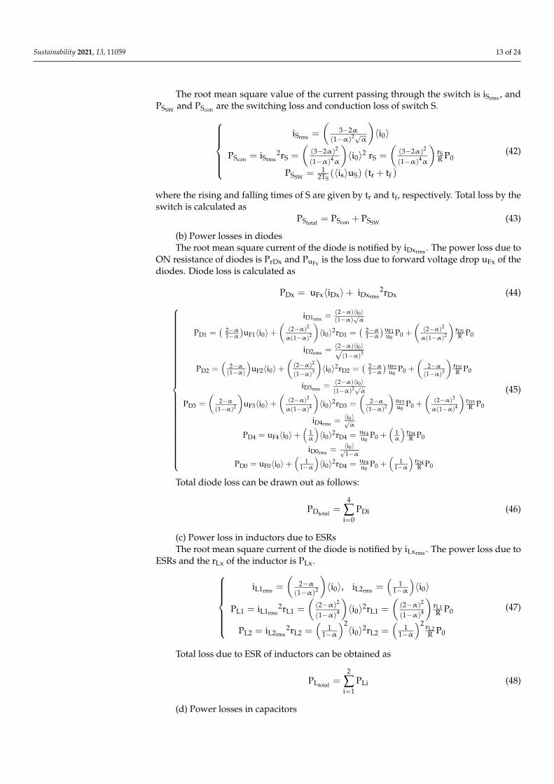
A detailed analysis of the proposed converter with similar non-isolated structures iscarried out in this section. The comparison is based on voltage gain, voltage stress, and thenumber of components in the converters, as listed in Table 1. Voltage gain is an importantindex to determine the performance of the converter. The voltage gain curve is shownin Figure 12. The proposed converter can achieve the highest voltage gain till duty ratio(α) of 0.6 after α > 0.6; topologies two and eight are greater than the proposed converter.Topology nine uses coupled inductors to boost the voltage gain up to eight times (notshown in Figures 12 and 13) because of the isolated category of DC-DC converters but hasthe maximum number of components compared to other converters listed in Table 1.
Sustainability 2021, 131, 1059 17 of 25
Figure 12. Voltage gain curve of the different topologies listed in Table 1.
Figure 13. Normalized switch voltage stress curve of the different topologies listed in Table 1.
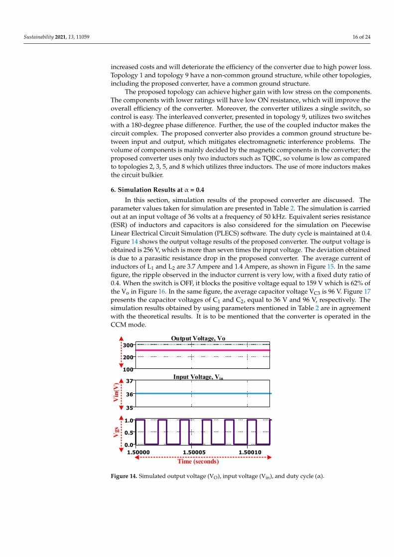
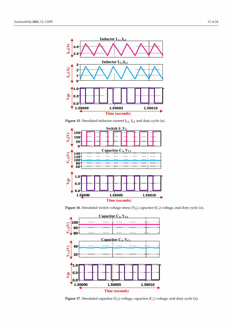
6. Simulation Results at α = 0.4 In this section, simulation results of the proposed converter are discussed. The pa-
rameter values taken for simulation are presented in Table 2. The simulation is carried out at an input voltage of 36 volts at a frequency of 50 kHz. Equivalent series resistance (ESR) of inductors and capacitors is also considered for the simulation on Piecewise Linear Elec-trical Circuit Simulation (PLECS) software. The duty cycle is maintained at 0.4. Figure 14 shows the output voltage results of the proposed converter. The output voltage is ob-tained is 256 V, which is more than seven times the input voltage. The deviation obtained is due to a parasitic resistance drop in the proposed converter. The average current of inductors of L1 and L2 are 3.7 Ampere and 1.4 Ampere, as shown in Figure 15. In the same figure, the ripple observed in the inductor current is very low, with a fixed duty ratio of 0.4. When the switch is OFF, it blocks the positive voltage equal to 159 V which is 62% of the Vo in Figure 16. In the same figure, the average capacitor voltage VC3 is 96 V. Figure 17
0
5
10
15
20
25
30
35
40
45
0.1 0.2 0.3 0.4 0.5 0.6 0.7 0.8
Vol
tage
Gai
n (K
CC
M)
Duty Ratio(α)
Proposed Topology-1 Topology-2/8Topology-3 Topology-4 Topology-5Topology-6 CQBC Topology-7
Proposed Converter
0
5
10
15
20
25
4 5 6 7 8 9 10 11 12 13 14 15
Switc
h V
olta
ge st
ress
(VS/V
in)
Voltage Gain (KCCM)
Proposed Topology-2/3/6/8
Topology-5 Topology-1/4
Topology-7
Proposed Converter
Figure 12. Voltage gain curve of the different topologies listed in Table 1.
Sustainability 2021, 13, 11059 15 of 24
Sustainability 2021, 131, 1059 17 of 25
Figure 12. Voltage gain curve of the different topologies listed in Table 1.
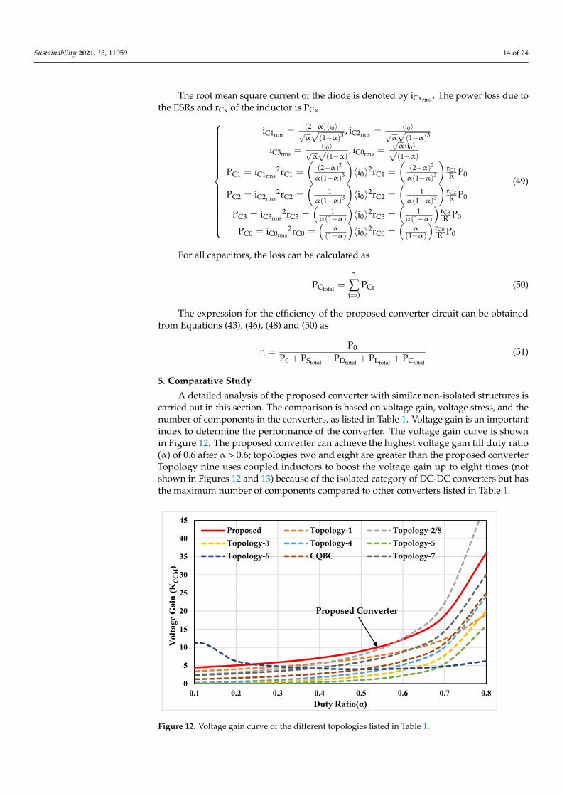
Figure 13. Normalized switch voltage stress curve of the different topologies listed in Table 1.
6. Simulation Results at α = 0.4 In this section, simulation results of the proposed converter are discussed. The pa-
rameter values taken for simulation are presented in Table 2. The simulation is carried out at an input voltage of 36 volts at a frequency of 50 kHz. Equivalent series resistance (ESR) of inductors and capacitors is also considered for the simulation on Piecewise Linear Elec-trical Circuit Simulation (PLECS) software. The duty cycle is maintained at 0.4. Figure 14 shows the output voltage results of the proposed converter. The output voltage is ob-tained is 256 V, which is more than seven times the input voltage. The deviation obtained is due to a parasitic resistance drop in the proposed converter. The average current of inductors of L1 and L2 are 3.7 Ampere and 1.4 Ampere, as shown in Figure 15. In the same figure, the ripple observed in the inductor current is very low, with a fixed duty ratio of 0.4. When the switch is OFF, it blocks the positive voltage equal to 159 V which is 62% of the Vo in Figure 16. In the same figure, the average capacitor voltage VC3 is 96 V. Figure 17
0
5
10
15
20
25
30
35
40
45
0.1 0.2 0.3 0.4 0.5 0.6 0.7 0.8
Vol
tage
Gai
n (K
CC
M)
Duty Ratio(α)
Proposed Topology-1 Topology-2/8Topology-3 Topology-4 Topology-5Topology-6 CQBC Topology-7
Proposed Converter
0
5
10
15
20
25
4 5 6 7 8 9 10 11 12 13 14 15
Switc
h V
olta
ge st
ress
(VS/V
in)
Voltage Gain (KCCM)
Proposed Topology-2/3/6/8
Topology-5 Topology-1/4
Topology-7
Proposed Converter
Figure 13. Normalized switch voltage stress curve of the different topologies listed in Table 1.
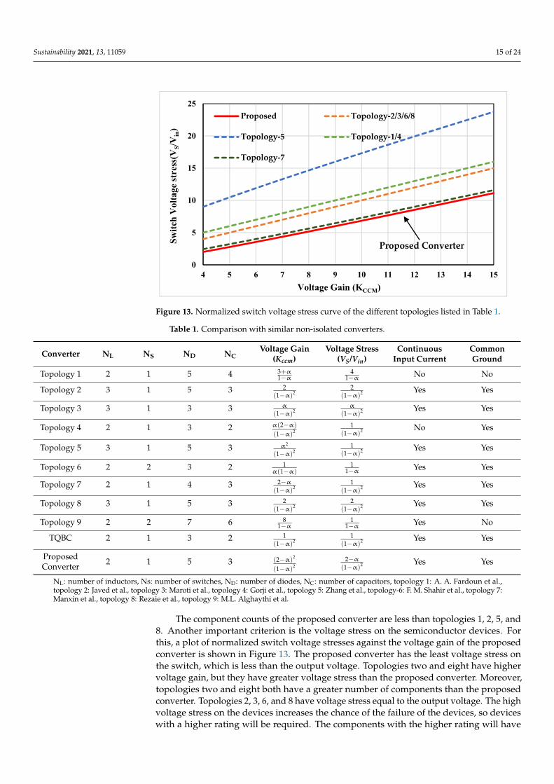
Table 1. Comparison with similar non-isolated converters.
Converter NL NS ND NCVoltage Gain
(Kccm)Voltage Stress
(VS/Vin)Continuous
Input CurrentCommonGround
Topology 1 2 1 5 4 3+α1−α
41−α No No
Topology 2 3 1 5 3 2(1−α)2
2(1−α)2 Yes Yes
Topology 3 3 1 3 3 α
(1−α)2α
(1−α)2 Yes Yes
Topology 4 2 1 3 2 α(2−α)
(1−α)21
(1−α)2 No Yes
Topology 5 3 1 5 3 α2
(1−α)21
(1−α)2 Yes Yes
Topology 6 2 2 3 2 1α(1−α)
11−α Yes Yes
Topology 7 2 1 4 3 2−α(1−α)2
1(1−α)2 Yes Yes
Topology 8 3 1 5 3 2(1−α)2
2(1−α)2 Yes Yes
Topology 9 2 2 7 6 81−α
11−α Yes No
TQBC 2 1 3 2 1(1−α)2
1(1−α)2 Yes Yes
ProposedConverter 2 1 5 3 (2−α)2
(1−α)22−α
(1−α)2 Yes Yes
NL: number of inductors, Ns: number of switches, ND: number of diodes, NC: number of capacitors, topology 1: A. A. Fardoun et al.,topology 2: Javed et al., topology 3: Maroti et al., topology 4: Gorji et al., topology 5: Zhang et al., topology-6: F. M. Shahir et al., topology 7:Manxin et al., topology 8: Rezaie et al., topology 9: M.L. Alghaythi et al.
The component counts of the proposed converter are less than topologies 1, 2, 5, and8. Another important criterion is the voltage stress on the semiconductor devices. Forthis, a plot of normalized switch voltage stresses against the voltage gain of the proposedconverter is shown in Figure 13. The proposed converter has the least voltage stress onthe switch, which is less than the output voltage. Topologies two and eight have highervoltage gain, but they have greater voltage stress than the proposed converter. Moreover,topologies two and eight both have a greater number of components than the proposedconverter. Topologies 2, 3, 6, and 8 have voltage stress equal to the output voltage. The highvoltage stress on the devices increases the chance of the failure of the devices, so deviceswith a higher rating will be required. The components with the higher rating will have
Sustainability 2021, 13, 11059 16 of 24
increased costs and will deteriorate the efficiency of the converter due to high power loss.Topology 1 and topology 9 have a non-common ground structure, while other topologies,including the proposed converter, have a common ground structure.
The proposed topology can achieve higher gain with low stress on the components.The components with lower ratings will have low ON resistance, which will improve theoverall efficiency of the converter. Moreover, the converter utilizes a single switch, socontrol is easy. The interleaved converter, presented in topology 9, utilizes two switcheswith a 180-degree phase difference. Further, the use of the coupled inductor makes thecircuit complex. The proposed converter also provides a common ground structure be-tween input and output, which mitigates electromagnetic interference problems. Thevolume of components is mainly decided by the magnetic components in the converter; theproposed converter uses only two inductors such as TQBC, so volume is low as comparedto topologies 2, 3, 5, and 8 which utilizes three inductors. The use of more inductors makesthe circuit bulkier.
6. Simulation Results at α = 0.4
In this section, simulation results of the proposed converter are discussed. Theparameter values taken for simulation are presented in Table 2. The simulation is carriedout at an input voltage of 36 volts at a frequency of 50 kHz. Equivalent series resistance(ESR) of inductors and capacitors is also considered for the simulation on PiecewiseLinear Electrical Circuit Simulation (PLECS) software. The duty cycle is maintained at 0.4.Figure 14 shows the output voltage results of the proposed converter. The output voltage isobtained is 256 V, which is more than seven times the input voltage. The deviation obtainedis due to a parasitic resistance drop in the proposed converter. The average current ofinductors of L1 and L2 are 3.7 Ampere and 1.4 Ampere, as shown in Figure 15. In the samefigure, the ripple observed in the inductor current is very low, with a fixed duty ratio of0.4. When the switch is OFF, it blocks the positive voltage equal to 159 V which is 62% ofthe Vo in Figure 16. In the same figure, the average capacitor voltage VC3 is 96 V. Figure 17presents the capacitor voltages of C1 and C2, equal to 36 V and 96 V, respectively. Thesimulation results obtained by using parameters mentioned in Table 2 are in agreementwith the theoretical results. It is to be mentioned that the converter is operated in theCCM mode.
Sustainability 2021, 131, 1059 18 of 25
presents the capacitor voltages of C1 and C2, equal to 36 V and 96 V, respectively. The simulation results obtained by using parameters mentioned in Table 2 are in agreement with the theoretical results. It is to be mentioned that the converter is operated in the CCM mode.
Table 2. Simulation parameters.
Parameters Value Input Voltage (V ) 36 V
Duty Cycle (α) 0.4 Frequency (f ) 50 kHz
Inductor (L1, L2) 330 μH, ESR = 0.92 Ω Capacitors (C1, C2, C3, andC0) 33 μF(each), ESR = 0.25 Ω
Power MOSFET SPW52N50C3, 0.07 Ω Diodes SF8L60USM
Load Resistance R = 300 Ω
100
200
300
35
36
37
1.50000 1.50005 1.500100.0
0.5
1.0
Time (seconds)
Vin
(V)
Vgs
Output Voltage, Vo
Input Voltage, Vin
Figure 14. Simulated output voltage (VO), input voltage (Vin), and duty cycle (α).
3.5
4.0
0123
1.50000 1.50005 1.500100.0
0.5
1.0
Time (seconds)
I L2(A
)I L
1(A)
Vgs
Inductor L1 , IL1
Inductor L2 ,IL2
Figure 15. Simulated inductor current IL1, IL2 and duty cycle (α).
Figure 14. Simulated output voltage (VO), input voltage (Vin), and duty cycle (α).
Sustainability 2021, 13, 11059 17 of 24
Sustainability 2021, 131, 1059 18 of 25
presents the capacitor voltages of C1 and C2, equal to 36 V and 96 V, respectively. The simulation results obtained by using parameters mentioned in Table 2 are in agreement with the theoretical results. It is to be mentioned that the converter is operated in the CCM mode.
Table 2. Simulation parameters.
Parameters Value Input Voltage (V ) 36 V
Duty Cycle (α) 0.4 Frequency (f ) 50 kHz
Inductor (L1, L2) 330 μH, ESR = 0.92 Ω Capacitors (C1, C2, C3, andC0) 33 μF(each), ESR = 0.25 Ω
Power MOSFET SPW52N50C3, 0.07 Ω Diodes SF8L60USM
Load Resistance R = 300 Ω
100
200
300
35
36
37
1.50000 1.50005 1.500100.0
0.5
1.0
Time (seconds)
Vin
(V)
Vgs
Output Voltage, Vo
Input Voltage, Vin
Figure 14. Simulated output voltage (VO), input voltage (Vin), and duty cycle (α).
3.5
4.0
0123
1.50000 1.50005 1.500100.0
0.5
1.0
Time (seconds)
I L2(A
)I L
1(A)
Vgs
Inductor L1 , IL1
Inductor L2 ,IL2
Figure 15. Simulated inductor current IL1, IL2 and duty cycle (α). Figure 15. Simulated inductor current IL1, IL2 and duty cycle (α).
Sustainability 2021, 131, 1059 19 of 25
050100150
6080100120140
1.50000 1.50005 1.500100.0
0.5
1.0
Time (seconds)
VS(V
)V
C3(V
)V
gs
Switch S ,VS
Capacitor C3, VC3
Figure 16. Simulated switch voltage stress (VS), capacitor (C3) voltage, and duty cycle (α).
8090100
20
40
1.50000 1.50005 1.500100.0
0.5
1.0
Time (seconds)
VC
2(V)
VC
1(V)
Vgs
Capacitor C2, VC2
Capacitor C1, VC1
Figure 17. Simulated capacitor (C2) voltage, capacitor (C1) voltage, and duty cycle (α).
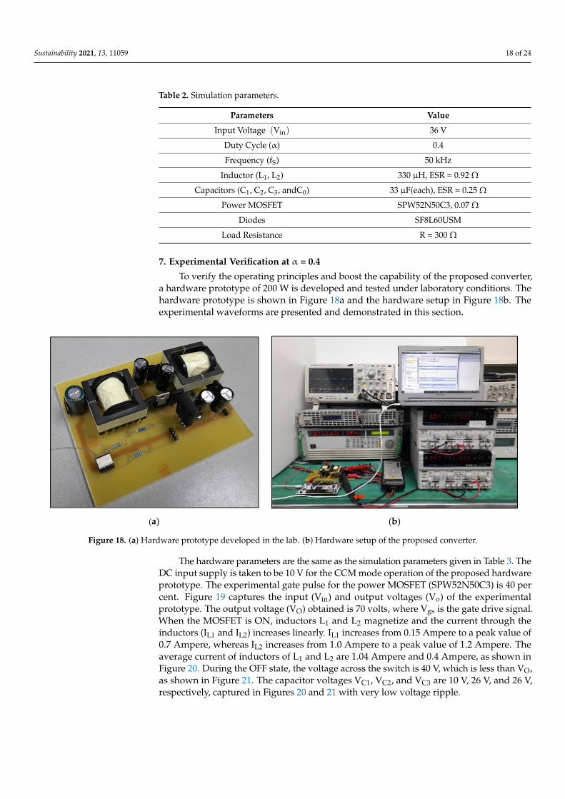
7. Experimental Verification at α = 0.4 To verify the operating principles and boost the capability of the proposed converter,
a hardware prototype of 200 W is developed and tested under laboratory conditions. The hardware prototype is shown in Figure 18a and the hardware setup in Figure 18b. The experimental waveforms are presented and demonstrated in this section.
Figure 16. Simulated switch voltage stress (VS), capacitor (C3) voltage, and duty cycle (α).
Sustainability 2021, 131, 1059 19 of 25
050100150
6080100120140
1.50000 1.50005 1.500100.0
0.5
1.0
Time (seconds)
VS(V
)V
C3(V
)V
gs
Switch S ,VS
Capacitor C3, VC3
Figure 16. Simulated switch voltage stress (VS), capacitor (C3) voltage, and duty cycle (α).
8090100
20
40
1.50000 1.50005 1.500100.0
0.5
1.0
Time (seconds)
VC
2(V)
VC
1(V)
Vgs
Capacitor C2, VC2
Capacitor C1, VC1
Figure 17. Simulated capacitor (C2) voltage, capacitor (C1) voltage, and duty cycle (α).
7. Experimental Verification at α = 0.4 To verify the operating principles and boost the capability of the proposed converter,
a hardware prototype of 200 W is developed and tested under laboratory conditions. The hardware prototype is shown in Figure 18a and the hardware setup in Figure 18b. The experimental waveforms are presented and demonstrated in this section.
Figure 17. Simulated capacitor (C2) voltage, capacitor (C1) voltage, and duty cycle (α).
Sustainability 2021, 13, 11059 18 of 24
Table 2. Simulation parameters.
Parameters Value
Input Voltage (Vin) 36 V
Duty Cycle (α) 0.4
Frequency (fS) 50 kHz
Inductor (L1, L2) 330 µH, ESR = 0.92 Ω
Capacitors (C1, C2, C3, andC0) 33 µF(each), ESR = 0.25 Ω
Power MOSFET SPW52N50C3, 0.07 Ω
Diodes SF8L60USM
Load Resistance R = 300 Ω
7. Experimental Verification at α = 0.4
To verify the operating principles and boost the capability of the proposed converter,a hardware prototype of 200 W is developed and tested under laboratory conditions. Thehardware prototype is shown in Figure 18a and the hardware setup in Figure 18b. Theexperimental waveforms are presented and demonstrated in this section.
Sustainability 2021, 131, 1059 20 of 25
(a) (b)
Figure 18. (a) Hardware prototype developed in the lab. (b) Hardware setup of the proposed converter.
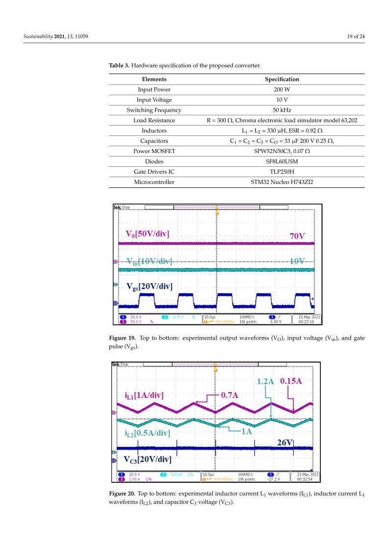
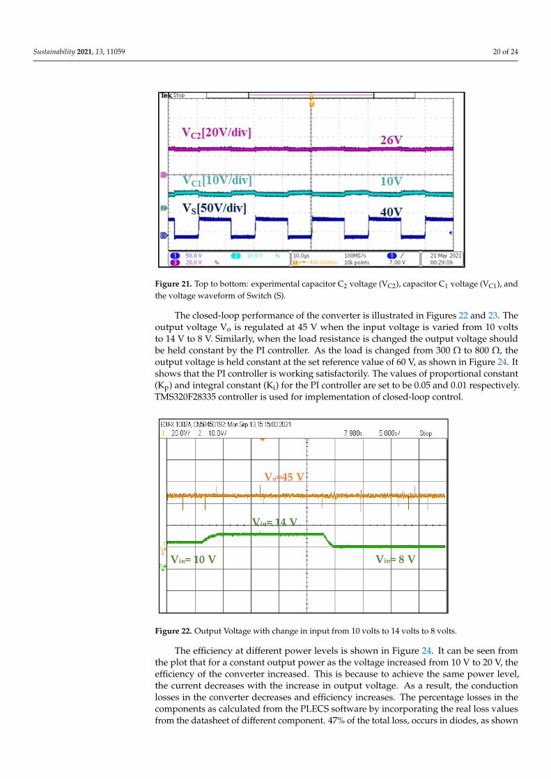
The hardware parameters are the same as the simulation parameters given in Table 3. The DC input supply is taken to be 10 V for the CCM mode operation of the proposed hardware prototype. The experimental gate pulse for the power MOSFET (SPW52N50C3) is 40 per cent. Figure 19 captures the input (Vin) and output voltages (Vo) of the experi-mental prototype. The output voltage (VO) obtained is 70 volts, where Vgs is the gate drive signal. When the MOSFET is ON, inductors L1 and L2 magnetize and the current through the inductors (IL1 and IL2) increases linearly. IL1 increases from 0.15 Ampere to a peak value of 0.7 Ampere, whereas IL2 increases from 1.0 Ampere to a peak value of 1.2 Ampere. The average current of inductors of L1 and L2 are 1.04 Ampere and 0.4 Ampere, as shown in Figure 20. During the OFF state, the voltage across the switch is 40 V, which is less than VO, as shown in Figure 21. The capacitor voltages VC1, VC2, and VC3 are 10 V, 26 V, and 26 V, respectively, captured in Figures 20 and 21 with very low voltage ripple.
Table 3. Hardware specification of the proposed converter.
Elements Specification Input Power 200 W
Input Voltage 10 V Switching Frequency 50 kHz
Load Resistance R = 300 Ω, Chroma electronic load simulator model 63,202 Inductors L1 = L2 = 330 μH, ESR = 0.92 Ω Capacitors C1 = C2 = C3 = CO = 33 μF 200 V 0.25 Ω,
Power MOSFET SPW52N50C3, 0.07 Ω Diodes SF8L60USM
Gate Drivers IC TLP250H Microcontroller STM32 Nucleo H743ZI2
Figure 18. (a) Hardware prototype developed in the lab. (b) Hardware setup of the proposed converter.
The hardware parameters are the same as the simulation parameters given in Table 3. TheDC input supply is taken to be 10 V for the CCM mode operation of the proposed hardwareprototype. The experimental gate pulse for the power MOSFET (SPW52N50C3) is 40 percent. Figure 19 captures the input (Vin) and output voltages (Vo) of the experimentalprototype. The output voltage (VO) obtained is 70 volts, where Vgs is the gate drive signal.When the MOSFET is ON, inductors L1 and L2 magnetize and the current through theinductors (IL1 and IL2) increases linearly. IL1 increases from 0.15 Ampere to a peak value of0.7 Ampere, whereas IL2 increases from 1.0 Ampere to a peak value of 1.2 Ampere. Theaverage current of inductors of L1 and L2 are 1.04 Ampere and 0.4 Ampere, as shown inFigure 20. During the OFF state, the voltage across the switch is 40 V, which is less than VO,as shown in Figure 21. The capacitor voltages VC1, VC2, and VC3 are 10 V, 26 V, and 26 V,respectively, captured in Figures 20 and 21 with very low voltage ripple.
Sustainability 2021, 13, 11059 19 of 24
Table 3. Hardware specification of the proposed converter.
Elements Specification
Input Power 200 W
Input Voltage 10 V
Switching Frequency 50 kHz
Load Resistance R = 300 Ω, Chroma electronic load simulator model 63,202
Inductors L1 = L2 = 330 µH, ESR = 0.92 Ω
Capacitors C1 = C2 = C3 = CO = 33 µF 200 V 0.25 Ω,
Power MOSFET SPW52N50C3, 0.07 Ω
Diodes SF8L60USM
Gate Drivers IC TLP250H
Microcontroller STM32 Nucleo H743ZI2Sustainability 2021, 131, 1059 21 of 25
Figure 19. Top to bottom: experimental output waveforms (VO), input voltage (Vin), and gate pulse (Vgs).
Figure 20. Top to bottom: experimental inductor current L1 waveforms (IL1), inductor current L1 waveforms (IL2), and capacitor C3 voltage (VC3).
Figure 21. Top to bottom: experimental capacitor C2 voltage (VC2), capacitor C1 voltage (VC1), and the voltage waveform of Switch (S).
Figure 19. Top to bottom: experimental output waveforms (VO), input voltage (Vin), and gatepulse (Vgs).
Sustainability 2021, 131, 1059 21 of 25
Figure 19. Top to bottom: experimental output waveforms (VO), input voltage (Vin), and gate pulse (Vgs).
Figure 20. Top to bottom: experimental inductor current L1 waveforms (IL1), inductor current L1 waveforms (IL2), and capacitor C3 voltage (VC3).
Figure 21. Top to bottom: experimental capacitor C2 voltage (VC2), capacitor C1 voltage (VC1), and the voltage waveform of Switch (S).
Figure 20. Top to bottom: experimental inductor current L1 waveforms (IL1), inductor current L1
waveforms (IL2), and capacitor C3 voltage (VC3).
Sustainability 2021, 13, 11059 20 of 24
Sustainability 2021, 131, 1059 21 of 25
Figure 19. Top to bottom: experimental output waveforms (VO), input voltage (Vin), and gate pulse (Vgs).
Figure 20. Top to bottom: experimental inductor current L1 waveforms (IL1), inductor current L1 waveforms (IL2), and capacitor C3 voltage (VC3).
Figure 21. Top to bottom: experimental capacitor C2 voltage (VC2), capacitor C1 voltage (VC1), and the voltage waveform of Switch (S).
Figure 21. Top to bottom: experimental capacitor C2 voltage (VC2), capacitor C1 voltage (VC1), andthe voltage waveform of Switch (S).
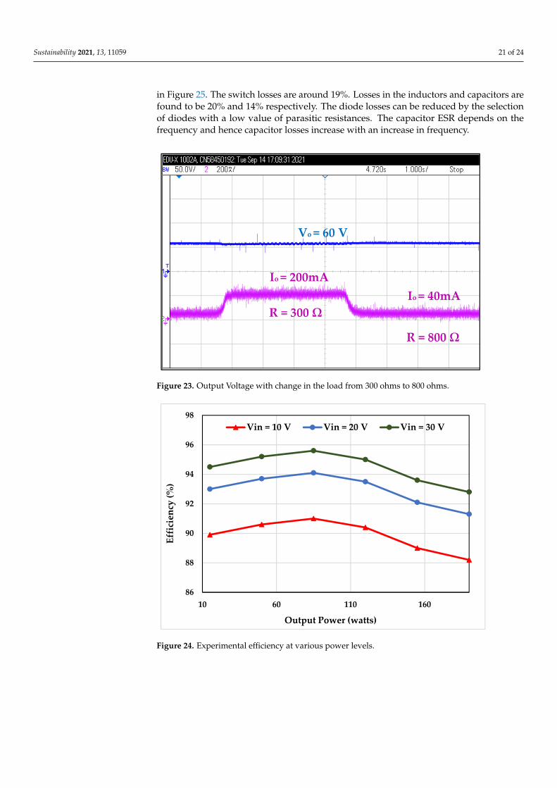
The closed-loop performance of the converter is illustrated in Figures 22 and 23. Theoutput voltage Vo is regulated at 45 V when the input voltage is varied from 10 voltsto 14 V to 8 V. Similarly, when the load resistance is changed the output voltage shouldbe held constant by the PI controller. As the load is changed from 300 Ω to 800 Ω, theoutput voltage is held constant at the set reference value of 60 V, as shown in Figure 24. Itshows that the PI controller is working satisfactorily. The values of proportional constant(Kp) and integral constant (Ki) for the PI controller are set to be 0.05 and 0.01 respectively.TMS320F28335 controller is used for implementation of closed-loop control.
Sustainability 2021, 131, 1059 22 of 25
The closed-loop performance of the converter is illustrated in Figures 22 and 23. The output voltage Vo is regulated at 45 V when the input voltage is varied from 10 volts to 14 V to 8 V. Similarly, when the load resistance is changed the output voltage should be held constant by the PI controller. As the load is changed from 300 Ω to 800 Ω, the output volt-age is held constant at the set reference value of 60 V, as shown in Figure 24. It shows that the PI controller is working satisfactorily. The values of proportional constant (Kp) and integral constant (Ki) for the PI controller are set to be 0.05 and 0.01 respectively. TMS320F28335 controller is used for implementation of closed-loop control.
The efficiency at different power levels is shown in Figure 24. It can be seen from the plot that for a constant output power as the voltage increased from 10 V to 20 V, the effi-ciency of the converter increased. This is because to achieve the same power level, the current decreases with the increase in output voltage. As a result, the conduction losses in the converter decreases and efficiency increases. The percentage losses in the components as calculated from the PLECS software by incorporating the real loss values from the datasheet of different component. 47% of the total loss, occurs in diodes, as shown in Fig-ure 25. The switch losses are around 19%. Losses in the inductors and capacitors are found to be 20% and 14% respectively. The diode losses can be reduced by the selection of diodes with a low value of parasitic resistances. The capacitor ESR depends on the frequency and hence capacitor losses increase with an increase in frequency.
Figure 22. Output Voltage with change in input from 10 volts to 14 volts to 8 volts.
Figure 23. Output Voltage with change in the load from 300 ohms to 800 ohms.
Vin= 8 V
Vin= 14 V
Vo=45 V
Vo = 60 V
R = 800 Ω
R = 300 Ω
Vin= 10 V
Io = 200mA Io = 40mA
Figure 22. Output Voltage with change in input from 10 volts to 14 volts to 8 volts.
The efficiency at different power levels is shown in Figure 24. It can be seen fromthe plot that for a constant output power as the voltage increased from 10 V to 20 V, theefficiency of the converter increased. This is because to achieve the same power level,the current decreases with the increase in output voltage. As a result, the conductionlosses in the converter decreases and efficiency increases. The percentage losses in thecomponents as calculated from the PLECS software by incorporating the real loss valuesfrom the datasheet of different component. 47% of the total loss, occurs in diodes, as shown
Sustainability 2021, 13, 11059 21 of 24
in Figure 25. The switch losses are around 19%. Losses in the inductors and capacitors arefound to be 20% and 14% respectively. The diode losses can be reduced by the selectionof diodes with a low value of parasitic resistances. The capacitor ESR depends on thefrequency and hence capacitor losses increase with an increase in frequency.
Sustainability 2021, 131, 1059 22 of 25
The closed-loop performance of the converter is illustrated in Figures 22 and 23. The output voltage Vo is regulated at 45 V when the input voltage is varied from 10 volts to 14 V to 8 V. Similarly, when the load resistance is changed the output voltage should be held constant by the PI controller. As the load is changed from 300 Ω to 800 Ω, the output volt-age is held constant at the set reference value of 60 V, as shown in Figure 24. It shows that the PI controller is working satisfactorily. The values of proportional constant (Kp) and integral constant (Ki) for the PI controller are set to be 0.05 and 0.01 respectively. TMS320F28335 controller is used for implementation of closed-loop control.
The efficiency at different power levels is shown in Figure 24. It can be seen from the plot that for a constant output power as the voltage increased from 10 V to 20 V, the effi-ciency of the converter increased. This is because to achieve the same power level, the current decreases with the increase in output voltage. As a result, the conduction losses in the converter decreases and efficiency increases. The percentage losses in the components as calculated from the PLECS software by incorporating the real loss values from the datasheet of different component. 47% of the total loss, occurs in diodes, as shown in Fig-ure 25. The switch losses are around 19%. Losses in the inductors and capacitors are found to be 20% and 14% respectively. The diode losses can be reduced by the selection of diodes with a low value of parasitic resistances. The capacitor ESR depends on the frequency and hence capacitor losses increase with an increase in frequency.
Figure 22. Output Voltage with change in input from 10 volts to 14 volts to 8 volts.
Figure 23. Output Voltage with change in the load from 300 ohms to 800 ohms.
Vin= 8 V
Vin= 14 V
Vo=45 V
Vo = 60 V
R = 800 Ω
R = 300 Ω
Vin= 10 V
Io = 200mA Io = 40mA
Figure 23. Output Voltage with change in the load from 300 ohms to 800 ohms.
Sustainability 2021, 131, 1059 23 of 25
Figure 24. Experimental efficiency at various power levels.
Figure 25. Power loss bifurcation of various components.
8. Discussion and Conclusions The proposed converter can achieve a voltage gain of more than 10 times at a duty
ratio of 0.6. The topology has a common ground structure with a single switch, so control is very easy with a reduced number of components. Due to parasitic resistances of com-ponents, the voltage gain of the proposed converter is severely affected at higher duty ratios. The total number of the elements in the proposed converter is less than the other converters for the same value of voltage gain. The maximum efficiency obtained was 94% at an input voltage of 20 V. The converter performance is found to be good in a closed-loop situation also with the PI controller. The PI controller is tuned to maintain a constant output voltage when the load or the input voltage changes. The converter is suitable for renewable energy applications for medium power applications due to the presence of con-tinuous input current and common ground between the input and the output sides.
86
88
90
92
94
96
98
10 60 110 160
Effi
cien
cy (%
)
Output Power (watts)
Vin = 10 V Vin = 20 V Vin = 30 V
Switch19%
Diodes47%
Inductors20%
Capacitors14%
Figure 24. Experimental efficiency at various power levels.

Sustainability 2021, 13, 11059 22 of 24
Sustainability 2021, 131, 1059 23 of 25
Figure 24. Experimental efficiency at various power levels.
Figure 25. Power loss bifurcation of various components.
8. Discussion and Conclusions The proposed converter can achieve a voltage gain of more than 10 times at a duty
ratio of 0.6. The topology has a common ground structure with a single switch, so control is very easy with a reduced number of components. Due to parasitic resistances of com-ponents, the voltage gain of the proposed converter is severely affected at higher duty ratios. The total number of the elements in the proposed converter is less than the other converters for the same value of voltage gain. The maximum efficiency obtained was 94% at an input voltage of 20 V. The converter performance is found to be good in a closed-loop situation also with the PI controller. The PI controller is tuned to maintain a constant output voltage when the load or the input voltage changes. The converter is suitable for renewable energy applications for medium power applications due to the presence of con-tinuous input current and common ground between the input and the output sides.
86
88
90
92
94
96
98
10 60 110 160
Effi
cien
cy (%
)
Output Power (watts)
Vin = 10 V Vin = 20 V Vin = 30 V
Switch19%
Diodes47%
Inductors20%
Capacitors14%
Figure 25. Power loss bifurcation of various components.
8. Discussion and Conclusions
The proposed converter can achieve a voltage gain of more than 10 times at a duty ratioof 0.6. The topology has a common ground structure with a single switch, so control is veryeasy with a reduced number of components. Due to parasitic resistances of components,the voltage gain of the proposed converter is severely affected at higher duty ratios. Thetotal number of the elements in the proposed converter is less than the other convertersfor the same value of voltage gain. The maximum efficiency obtained was 94% at an inputvoltage of 20 V. The converter performance is found to be good in a closed-loop situationalso with the PI controller. The PI controller is tuned to maintain a constant output voltagewhen the load or the input voltage changes. The converter is suitable for renewable energyapplications for medium power applications due to the presence of continuous inputcurrent and common ground between the input and the output sides.
Author Contributions: Conceptualization, S.K., A.M., M.Z. and M.T.; Formal analysis, S.K., A.M.,M.Z. and M.T.; Funding acquisition, M.T., C.-H.L., B.A. and A.A.; Investigation, S.K., A.M., M.Z.,M.T. and J.A.; Methodology, S.K., A.M., M.T. and J.A.; Supervision, M.Z.; Writing—original draft,S.K., A.M. and M.Z.; Writing—review and editing, S.K., M.T., C.-H.L., J.A., B.A. and A.A. All authorshave read and agreed to the published version of the manuscript.
Funding: This research was funded by the Ministry of Science and Technology, Taiwan, R.O.C., grantnumber MOST 110-2622-8-005-005-TE1.
Institutional Review Board Statement: Not applicable.
Informed Consent Statement: Not applicable.
Data Availability Statement: Not applicable.
Acknowledgments: The authors would like to acknowledge the financial support from Taif Univer-sity Researchers Supporting Project Number (TURSP-2020/121), Taif University, Taif, Saudi Arabia.This publication was made possible by the Collaborative Research Grant Scheme (CRGS) projectsponsored by the Capability Systems Centre, University of New South Wales—Canberra, Australia,to the Department of Electrical Engineering, Aligarh Muslim University, India, project grant no:(CRGS/Mohd Tariq/01 and CRGS/Mohd Tariq/02). The authors also acknowledge the supportprovided by the Hardware-In-the-Loop (HIL) Lab, Department of Electrical Engineering, AligarhMuslim University, India.
Conflicts of Interest: The authors declare no conflict of interest.

Sustainability 2021, 13, 11059 23 of 24
References1. Blaabjerg, F.; Ionel, D.M. Renewable Energy Devices and Systems—State-of-the-Art Technology, Research and Development,
Challenges and Future Trends. Electr. Power Compon. Syst. 2015, 43, 1319–1328. [CrossRef]2. Mohamad, F.; Teh, J.; Lai, C.-M. Optimum allocation of battery energy storage systems for power grid enhanced with solar energy.
Energy 2021, 223, 120105. [CrossRef]3. Mohamad, F.; Teh, J.; Abunima, H. Multi-Objective Optimization of Solar/Wind Penetration in Power Generation Systems. IEEE
Access 2019, 7, 169094–169106. [CrossRef]4. Teh, J.; Cotton, I. Reliability Impact of Dynamic Thermal Rating System in Wind Power Integrated Network. IEEE Trans. Reliab.
2015, 65, 1081–1089. [CrossRef]5. Teh, J. Adequacy Assessment of Wind Integrated Generating Systems Incorporating Demand Response and Battery Energy
Storage System. Energies 2018, 11, 2649. [CrossRef]6. Fotopoulou, M.; Rakopoulos, D.; Trigkas, D.; Stergiopoulos, F.; Blanas, O.; Voutetakis, S. State of the Art of Low and Medium
Voltage Direct Current (DC) Microgrids. Energies 2021, 14, 5595. [CrossRef]7. Kumar, D.; Zare, F.; Ghosh, A. DC Microgrid Technology: System Architectures, AC Grid Interfaces, Grounding Schemes, Power
Quality, Communication Networks, Applications, and Standardizations Aspects. IEEE Access 2017, 5, 12230–12256. [CrossRef]8. Dragicevic, T.; Lu, X.; Vasquez, J.C.; Guerrero, J. DC Microgrids—Part II: A Review of Power Architectures, Applications, and
Standardization Issues. IEEE Trans. Power Electron. 2016, 31, 3528–3549. [CrossRef]9. Forouzesh, M.; Siwakoti, Y.P.; Gorji, S.A.; Blaabjerg, F.; Lehman, B. Step-Up DC–DC Converters: A Comprehensive Review of
Voltage-Boosting Techniques, Topologies, and Applications. IEEE Trans. Power Electron. 2017, 32, 9143–9178. [CrossRef]10. Mahmood, A.; Zaid, M.; Ahmad, J.; Khan, M.A.; Khan, S.; Sifat, Z.; Lin, C.-H.; Sarwar, A.; Tariq, M.; Alamri, B. A Non-Inverting
High Gain DC-DC Converter With Continuous Input Current. IEEE Access 2021, 9, 54710–54721. [CrossRef]11. Khan, S.; Mahmood, A.; Tariq, M.; Zaid, M.; Khan, I.; Rahman, S. Improved Dual Switch Non-Isolated High Gain Boost Converter
for DC microgrid Application. In Proceedings of the 2021 IEEE Texas Power and Energy Conference (TPEC), College Station, TX,USA, 2–5 February 2021; pp. 1–6. [CrossRef]
12. Wu, G.; Ruan, X.; Ye, Z. Nonisolated High Step-Up DC–DC Converters Adopting Switched-Capacitor Cell. IEEE Trans. Ind.Electron. 2015, 62, 383–393. [CrossRef]
13. Zaid, M.; Khan, S.; Siddique, M.D.; Sarwar, A.; Ahmad, J.; Sarwer, Z.; Iqbal, A. A transformerless high gain dc–dc boost converterwith reduced voltage stress. Int. Trans. Electr. Energy Syst. 2021, 31, e12877. [CrossRef]
14. Khan, S.; Zaid, M.; Mahmood, A.; Ahmad, J.; Alam, A. A Single Switch High Gain DC-DC converter with Reduced Voltage Stress.In Proceedings of the 2020 IEEE 7th Uttar Pradesh Section International Conference on Electrical, Electronics and ComputerEngineering (UPCON), Prayagraj, India, 27–29 November 2020; pp. 1–6. [CrossRef]
15. Khan, S.; Mahmood, A.; Zaid, M.; Tariq, M.; Sadaf, S. A Single Inductor, Single Switch High Gain DC-DC Boost Converter. InProceedings of the 2020 IEEE International Women in Engineering (WIE) Conference on Electrical and Computer Engineering(WIECON-ECE), Bhubaneswar, India, 26–27 December 2020; pp. 98–101. [CrossRef]
16. Ahmad, J.; Zaid, M.; Sarwar, A.; Tariq, M.; Sarwer, Z. A New Transformerless Quadratic Boost Converter with High Voltage Gain.Smart Sci. 2020, 8, 163–183. [CrossRef]
17. Rezaie, M.; Abbasi, V. Effective combination of quadratic boost converter with voltage multiplier cell to increase voltage gain. IETPower Electron. 2020, 13, 2322–2333. [CrossRef]
18. Maroti, P.K.; Padmanaban, S.; Holm-Nielsen, J.B.; Bhaskar, M.S.; Meraj, M.; Iqbal, A. A New Structure of High Voltage GainSEPIC Converter for Renewable Energy Applications. IEEE Access 2019, 7, 89857–89868. [CrossRef]
19. Zhang, N.; Zhang, G.; See, K.; Zhang, B. A Single-Switch Quadratic Buck–Boost Converter With Continuous Input Port Currentand Continuous Output Port Current. IEEE Trans. Power Electron. 2017, 33, 4157–4166. [CrossRef]
20. Gorji, S.A.; Mostaan, A.; My, H.T.; Ektesabi, M. Non-isolated buck–boost dc–dc converter with quadratic voltage gain ratio. IETPower Electron. 2019, 12, 1425–1433. [CrossRef]
21. Chen, M.; Li, K.; Hu, J.; Ioinovici, A. Hybrid switched-capacitor quadratic boost converters with very high DC gain and lowvoltage stress on their semiconductor devices. In Proceedings of the 2016 IEEE Energy Conversion Congress and Exposition(ECCE), Milwaukee, WI, USA, 18–22 September 2016; pp. 1–8. [CrossRef]
22. Dasari, R.K.; Immanuel, D.G. Comprehensive Review of Single Switch DC-DC Converters for Voltage Lift in RES Application. InProceedings of the 2018 International Conference on Power, Energy, Control and Transmission Systems (ICPECTS), Chennai,India, 22–23 February 2018; pp. 281–288. [CrossRef]
23. Azar, M.A.; Shahir, F.M.; Taher, B. New single switch topology for non-isolated boost DC-DC converter based on voltage-lifttechnique. In Proceedings of the 2018 IEEE 12th International Conference on Compatibility, Power Electronics and PowerEngineering (CPE-POWERENG 2018), Doha, Qatar, 10–12 April 2018; pp. 1–6. [CrossRef]
24. Zhu, M.; Wang, T.; Luo, F.L. Analysis of voltage-lift-type boost converters. In Proceedings of the 2012 7th IEEE Conference onIndustrial Electronics and Applications (ICIEA), Singapore, 18–20 July 2012; pp. 214–219. [CrossRef]
25. Laha, A. A High Voltage Gain Quadratic Boost Converter using a Voltage Doubler and Voltage-Lift Technique. In Proceedings ofthe 2020 IEEE International Conference on Power Electronics, Smart Grid and Renewable Energy (PESGRE2020), Cochin, India,2–4 January 2020; pp. 1–6. [CrossRef]

Sustainability 2021, 13, 11059 24 of 24
26. Ramanaiah, G.V.; Sundar, S.N.S.; Ananthakrishnan, P.; Manikanta, K. Design and Analysis of Voltage Lift Technique Based BoostDC-DC Converter. In Proceedings of the 2019 International Conference on Power Electronics Applications and Technology inPresent Energy Scenario (PETPES), Mangalore, India, 29–31 August 2019; pp. 1–6. [CrossRef]
27. Zaid, M.; Lin, C.-H.; Khan, S.; Ahmad, J.; Tariq, M.; Mahmood, A.; Sarwar, A.; Alamri, B.; Alahmadi, A. A Family of Transformer-less Quadratic Boost High Gain DC-DC Converters. Energies 2021, 14, 4372. [CrossRef]
28. Khan, S.; Zaid, M.; Mahmood, A.; Nooruddin, A.S.; Ahmad, J.; Alghaythi, M.L.; Alamri, B.; Tariq, M.; Sarwar, A.; Lin, C.-H. ANew Transformerless Ultra High Gain DC–DC Converter for DC Microgrid Application. IEEE Access 2021, 9, 124560–124582.[CrossRef]
29. Shahir, F.M.; Babaei, E.; Farsadi, M. Extended Topology for a Boost DC–DC Converter. IEEE Trans. Power Electron. 2018, 34,2375–2384. [CrossRef]
30. Alghaythi, M.L.; O’Connell, R.M.; Islam, N.E.; Khan, M.M.S.; Guerrero, J.M. A High Step-Up Interleaved DC-DC Converter WithVoltage Multiplier and Coupled Inductors for Renewable Energy Systems. IEEE Access 2020, 8, 123165–123174. [CrossRef]