
Development of 50kW Isolated DC/DC Converter with High-Voltage IGBTs
6
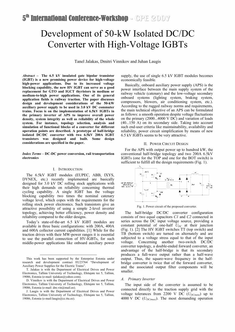
5 5 t t h h I I n n t t e e r r n n a a t t i i o o n n a a l l C C o o n n f f e e r r e e n n c c e e - - W W o o r r k k s s h h o o p p - C P E 2 0 0 7 Development of 50-kW Isolated DC/DC Converter with High-Voltage IGBTs Tanel Jalakas, Dmitri Vinnikov and Juhan Laugis Abstract – The 6.5 kV insulated gate bipolar transistor (IGBT) is a new promising power device for high-voltage high-power applications. Due to its increased voltage blocking capability, the new HV IGBT can serve as a good replacement for GTO and IGCT thyristors in medium or medium-to-high power applications. One of its general application fields is railway traction. The paper discusses design and development considerations of the 50-kW auxiliary power supply to be used in 3.0 kV DC commuter trains. Focus is on the implementation of 6.5kV IGBTs in the primary inverter of APS to improve overall power density, system integrity as well as reliability of the whole system. For instance, topology selection, analysis and simulation of functional blocks of a converter for different operation points are described. A prototype of half-bridge isolated DC/DC converter with two 6.5kV 200A IGBT transistors was designed and built. Some design considerations are specified in the paper. Index Terms – DC-DC power conversion, rail transportation electronics I. INTRODUCTION The 6.5kV IGBT modules (EUPEC, ABB, IXYS, DYNEX, etc.) recently implemented are basically designed for 3.0 kV DC rolling stock applications with their high demands on reliability concerning thermal cycling capability. A single IGBT has the voltage blocking capability two times the nominal catenary voltage level, which copes with the requirements for the rolling stock power electronics. Such transistors give an attractive possibility of using a simple 2-level inverter topology, achieving better efficiency, power density and reliability compared to the older designs. Today’s state-of-the-art 6.5 kV IGBT modules are available in three basic configurations: with 200A, 400A and 600A collector current capabilities. [1] While for the traction drives with their MW-power ranges it is essential to use the parallel connection of HV-IGBTs, for such middle-power applications like onboard auxiliary power This work has been supported by the Enterprise Estonia under research and development contract EU23764 “Development of Auxiliary Power Supplies for the Electric Trains”. T. Jalakas is with the Department of Electrical Drives and Power Electronics, Tallinn University of Technology, Ehitajate tee 5, Tallinn, 19086, Estonia (e-mail: [email protected]). D. Vinnikov is with the Department of Electrical Drives and Power Electronics, Tallinn University of Technology, Ehitajate tee 5, Tallinn, 19086, Estonia (e-mail: [email protected]). J. Laugis is with the Department of Electrical Drives and Power Electronics, Tallinn University of Technology, Ehitajate tee 5, Tallinn, 19086, Estonia (e-mail:[email protected]). supply, the use of single 6.5 kV IGBT modules becomes economically feasible. Basically, onboard auxiliary power supply (APS) is the power interface between the main supply system of the railway vehicle (catenary) and the low-voltage secondary onboard systems (lighting system, braking system, compressors, blowers, air conditioning system, etc.). According to the rugged railway norms and requirements, the main technical objective of an APS can be formulated as follows: a smooth operation despite voltage fluctuations on the primary (2000...4000 V DC) and variation of loads (40...150 A) on its secondary side. Taking into account such end-user criteria like maintainability, availability and reliability, power circuit simplification by means of new 6.5 kV IGBTs seems to be very attractive. II. POWER CIRCUIT DESIGN For the APS with output power up to hundred kW, the conventional half-bridge topology and two 200A 6.5kV IGBTs (one for the TOP and one for the BOT switch) is sufficient to fulfill all the design requirements (Fig. 1). Fig. 1. Power circuit of the proposed converter. The half-bridge DC/DC converter configuration consists of two equal capacitors C1 and C2 connected in series across the DC input voltage source, providing a constant potential of one-half U DC at their junction (Fig. 1). [2] The HV IGBT switches TT (top switch) and TB (bottom switch) are turned on alternately and are subjected to a voltage stress equal to that of the input voltage. Concerning another two-switch DC/DC converter topology, a double-ended forward converter, an andvantage of the half-bridge is that its secondary produces a full-wave output rather than a half-wave output. Thus, the square-wave frequency in the half- bridge converter is twice that of the forward converter, and the associated output filter components will be smaller. A. Primary Inverter The input side of the converter is assumed to be connected directly to the traction supply grid with the voltage tolerances from 2200 V DC (U DC(min) ) up to 4000 V DC (U DC(max) ). The most demanding operation
-
Upload
independent -
Category
Documents
-
view
1 -
download
0
Transcript of Development of 50kW Isolated DC/DC Converter with High-Voltage IGBTs
55tthh IInntteerrnnaattiioonnaall CCoonnffeerreennccee--WWoorrkksshhoopp - CPE 2007
Development of 50-kW Isolated DC/DC Converter with High-Voltage IGBTs
Tanel Jalakas, Dmitri Vinnikov and Juhan Laugis
Abstract – The 6.5 kV insulated gate bipolar transistor (IGBT) is a new promising power device for high-voltage high-power applications. Due to its increased voltage blocking capability, the new HV IGBT can serve as a good replacement for GTO and IGCT thyristors in medium or medium-to-high power applications. One of its general application fields is railway traction. The paper discusses design and development considerations of the 50-kW auxiliary power supply to be used in 3.0 kV DC commuter trains. Focus is on the implementation of 6.5kV IGBTs in the primary inverter of APS to improve overall power density, system integrity as well as reliability of the whole system. For instance, topology selection, analysis and simulation of functional blocks of a converter for different operation points are described. A prototype of half-bridge isolated DC/DC converter with two 6.5kV 200A IGBT transistors was designed and built. Some design considerations are specified in the paper.
Index Terms – DC-DC power conversion, rail transportation electronics
I. INTRODUCTION The 6.5kV IGBT modules (EUPEC, ABB, IXYS,
DYNEX, etc.) recently implemented are basically designed for 3.0 kV DC rolling stock applications with their high demands on reliability concerning thermal cycling capability. A single IGBT has the voltage blocking capability two times the nominal catenary voltage level, which copes with the requirements for the rolling stock power electronics. Such transistors give an attractive possibility of using a simple 2-level inverter topology, achieving better efficiency, power density and reliability compared to the older designs.
Today’s state-of-the-art 6.5 kV IGBT modules are available in three basic configurations: with 200A, 400A and 600A collector current capabilities. [1] While for the traction drives with their MW-power ranges it is essential to use the parallel connection of HV-IGBTs, for such middle-power applications like onboard auxiliary power
This work has been supported by the Enterprise Estonia under
research and development contract EU23764 “Development of Auxiliary Power Supplies for the Electric Trains”.
T. Jalakas is with the Department of Electrical Drives and Power Electronics, Tallinn University of Technology, Ehitajate tee 5, Tallinn, 19086, Estonia (e-mail: [email protected]).
D. Vinnikov is with the Department of Electrical Drives and Power Electronics, Tallinn University of Technology, Ehitajate tee 5, Tallinn, 19086, Estonia (e-mail: [email protected]).
J. Laugis is with the Department of Electrical Drives and Power Electronics, Tallinn University of Technology, Ehitajate tee 5, Tallinn, 19086, Estonia (e-mail:[email protected]).
supply, the use of single 6.5 kV IGBT modules becomes economically feasible.
Basically, onboard auxiliary power supply (APS) is the power interface between the main supply system of the railway vehicle (catenary) and the low-voltage secondary onboard systems (lighting system, braking system, compressors, blowers, air conditioning system, etc.). According to the rugged railway norms and requirements, the main technical objective of an APS can be formulated as follows: a smooth operation despite voltage fluctuations on the primary (2000...4000 V DC) and variation of loads (40...150 A) on its secondary side. Taking into account such end-user criteria like maintainability, availability and reliability, power circuit simplification by means of new 6.5 kV IGBTs seems to be very attractive.
II. POWER CIRCUIT DESIGN For the APS with output power up to hundred kW, the
conventional half-bridge topology and two 200A 6.5kV IGBTs (one for the TOP and one for the BOT switch) is sufficient to fulfill all the design requirements (Fig. 1).
Fig. 1. Power circuit of the proposed converter.
The half-bridge DC/DC converter configuration consists of two equal capacitors C1 and C2 connected in series across the DC input voltage source, providing a constant potential of one-half UDC at their junction (Fig. 1). [2] The HV IGBT switches TT (top switch) and TB (bottom switch) are turned on alternately and are subjected to a voltage stress equal to that of the input voltage. Concerning another two-switch DC/DC converter topology, a double-ended forward converter, an andvantage of the half-bridge is that its secondary produces a full-wave output rather than a half-wave output. Thus, the square-wave frequency in the half-bridge converter is twice that of the forward converter, and the associated output filter components will be smaller.
A. Primary Inverter The input side of the converter is assumed to be
connected directly to the traction supply grid with the voltage tolerances from 2200 V DC (UDC(min)) up to 4000 V DC (UDC(max)). The most demanding operation
55tthh IInntteerrnnaattiioonnaall CCoonnffeerreennccee--WWoorrkksshhoopp - CPE 2007
point is at the minimum input voltage and at the rated load conditions (i.e., maximum duty cycle operation). It is essential to prevent even short-time simultaneous conduction of TT and TB switches in these demanding conditions - it leads to the short circuit across the supply voltage and to the destruction of the converter. It means that the maximum on-state time ton(max) of each switch in the half-bridge must be set at 80% of a half-period to ensure that this does not happen. Pulse width at the maximum input voltage is minimal and may be determined as
)1(2
44.040002200
(max)(max)(max)
(min)(min) ⎟
⎠⎞
⎜⎝⎛=== sw
ononDC
DCon
TttUU
t
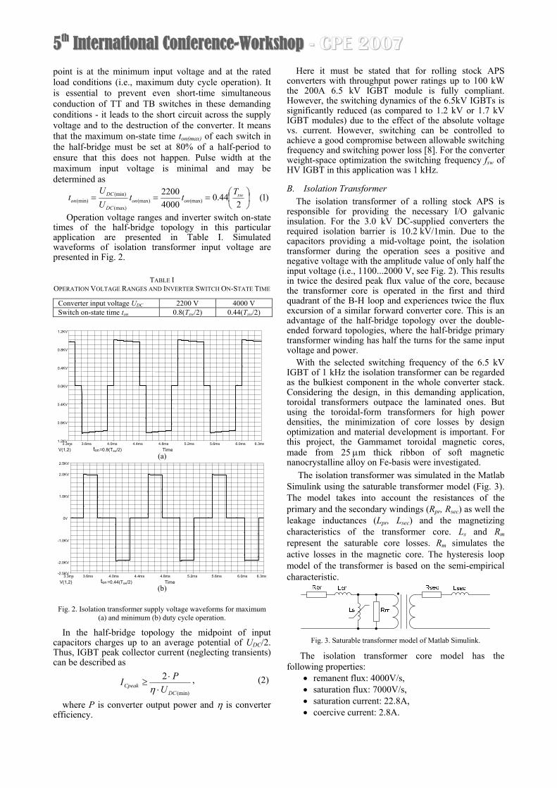
Operation voltage ranges and inverter switch on-state times of the half-bridge topology in this particular application are presented in Table I. Simulated waveforms of isolation transformer input voltage are presented in Fig. 2.
TABLE I OPERATION VOLTAGE RANGES AND INVERTER SWITCH ON-STATE TIME
Converter input voltage UDC 2200 V 4000 V Switch on-state time ton 0.8(Tsw/2) 0.44(Tsw/2)
Time 3.6ms 4.0ms 4.4ms 4.8ms 5.2ms 5.6ms 6.0ms3.3ms 6.3ms
V(1,2) D=0.8(Tsw/2)
1.2KV
0.8KV
0.4KV
0.0KV
0.4KV
0.8KV
1.2KV
Time3.6ms 4.0ms 4.4ms 4.8ms 5.2ms 5.6ms 6.0ms3.3ms 6.3ms
V(1,2) D=0.44(Tsw/2)
-2.0KV
-1.0KV
0V
1.0KV
2.0KV
-2.5KV
2.5KV
(a)
(b)
ton
ton
Fig. 2. Isolation transformer supply voltage waveforms for maximum
(a) and minimum (b) duty cycle operation.
In the half-bridge topology the midpoint of input capacitors charges up to an average potential of UDC/2. Thus, IGBT peak collector current (neglecting transients) can be described as
(min)
2
DCCpeak U
PI⋅
⋅≥
η, (2)
where P is converter output power and η is converter efficiency.
Here it must be stated that for rolling stock APS converters with throughput power ratings up to 100 kW the 200A 6.5 kV IGBT module is fully compliant. However, the switching dynamics of the 6.5kV IGBTs is significantly reduced (as compared to 1.2 kV or 1.7 kV IGBT modules) due to the effect of the absolute voltage vs. current. However, switching can be controlled to achieve a good compromise between allowable switching frequency and switching power loss [8]. For the converter weight-space optimization the switching frequency fsw of HV IGBT in this application was 1 kHz.
B. Isolation Transformer The isolation transformer of a rolling stock APS is
responsible for providing the necessary I/O galvanic insulation. For the 3.0 kV DC-supplied converters the required isolation barrier is 10.2 kV/1min. Due to the capacitors providing a mid-voltage point, the isolation transformer during the operation sees a positive and negative voltage with the amplitude value of only half the input voltage (i.e., 1100...2000 V, see Fig. 2). This results in twice the desired peak flux value of the core, because the transformer core is operated in the first and third quadrant of the B-H loop and experiences twice the flux excursion of a similar forward converter core. This is an advantage of the half-bridge topology over the double-ended forward topologies, where the half-bridge primary transformer winding has half the turns for the same input voltage and power.
With the selected switching frequency of the 6.5 kV IGBT of 1 kHz the isolation transformer can be regarded as the bulkiest component in the whole converter stack. Considering the design, in this demanding application, toroidal transformers outpace the laminated ones. But using the toroidal-form transformers for high power densities, the minimization of core losses by design optimization and material development is important. For this project, the Gammamet toroidal magnetic cores, made from 25 μm thick ribbon of soft magnetic nanocrystalline alloy on Fe-basis were investigated.
The isolation transformer was simulated in the Matlab Simulink using the saturable transformer model (Fig. 3). The model takes into account the resistances of the primary and the secondary windings (Rpr, Rsec) as well the leakage inductances (Lpr, Lsec) and the magnetizing characteristics of the transformer core. Ls and Rm represent the saturable core losses. Rm simulates the active losses in the magnetic core. The hysteresis loop model of the transformer is based on the semi-empirical characteristic.
Fig. 3. Saturable transformer model of Matlab Simulink.
The isolation transformer core model has the following properties:
• remanent flux: 4000V/s, • saturation flux: 7000V/s, • saturation current: 22.8A, • coercive current: 2.8A.
55tthh IInntteerrnnaattiioonnaall CCoonnffeerreennccee--WWoorrkksshhoopp - CPE 2007
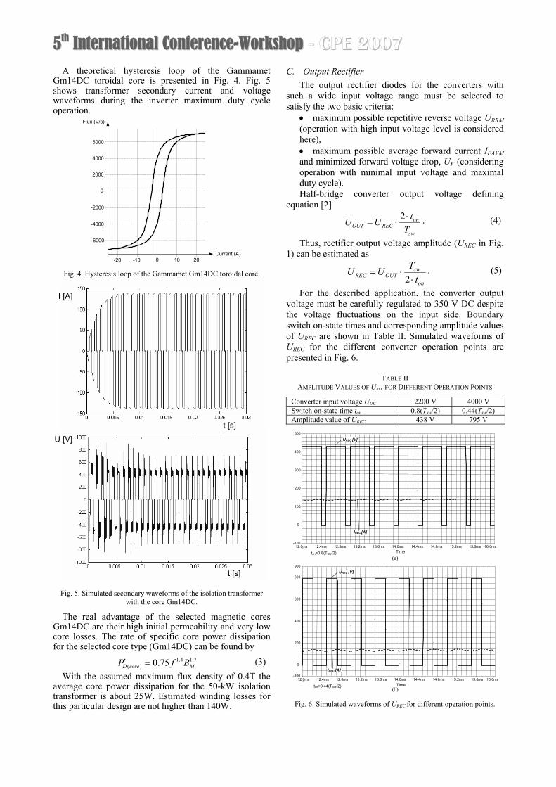
A theoretical hysteresis loop of the Gammamet Gm14DC toroidal core is presented in Fig. 4. Fig. 5 shows transformer secondary current and voltage waveforms during the inverter maximum duty cycle operation.
Current (A)
Flux (V/s)
0 10 20-20 -10
0
2000
4000
6000
-2000
-4000
-6000
Fig. 4. Hysteresis loop of the Gammamet Gm14DC toroidal core.
I [A]
U [V]
t [s]
t [s] Fig. 5. Simulated secondary waveforms of the isolation transformer
with the core Gm14DC.
The real advantage of the selected magnetic cores Gm14DC are their high initial permeability and very low core losses. The rate of specific core power dissipation for the selected core type (Gm14DC) can be found by
(3) 7.14.1)( 75.0 McoreD BfP =′
With the assumed maximum flux density of 0.4T the average core power dissipation for the 50-kW isolation transformer is about 25W. Estimated winding losses for this particular design are not higher than 140W.
C. Output Rectifier The output rectifier diodes for the converters with
such a wide input voltage range must be selected to satisfy the two basic criteria:
• maximum possible repetitive reverse voltage URRM (operation with high input voltage level is considered here), • maximum possible average forward current IFAVM and minimized forward voltage drop, UF (considering operation with minimal input voltage and maximal duty cycle). Half-bridge converter output voltage defining
equation [2]
sw
onRECOUT T
tUU ⋅⋅=2 . (4)
Thus, rectifier output voltage amplitude (UREC in Fig. 1) can be estimated as
on
swOUTREC t
TUU⋅
⋅=2
. (5)
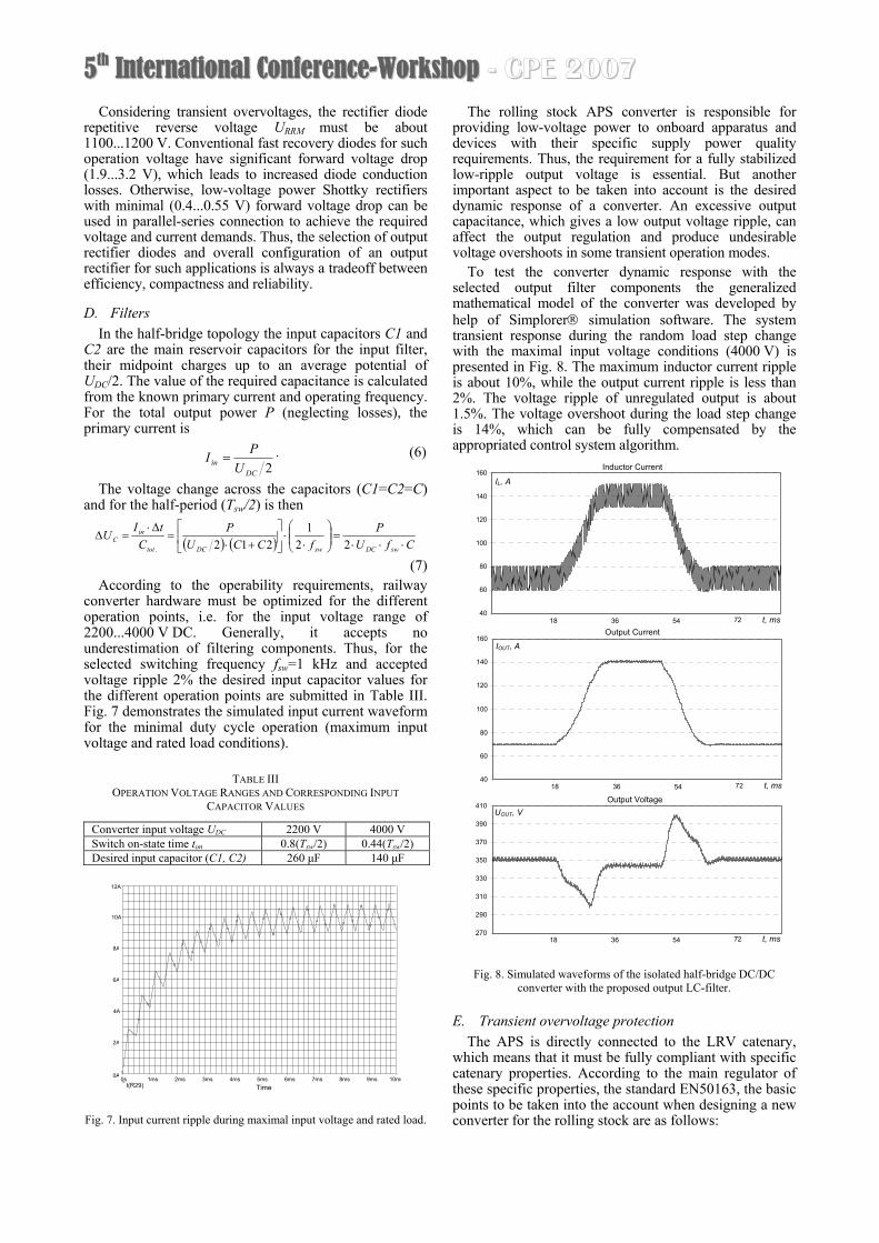
For the described application, the converter output voltage must be carefully regulated to 350 V DC despite the voltage fluctuations on the input side. Boundary switch on-state times and corresponding amplitude values of UREC are shown in Table II. Simulated waveforms of UREC
for the different converter operation points are presented in Fig. 6.
TABLE II AMPLITUDE VALUES OF UREC FOR DIFFERENT OPERATION POINTS
Converter input voltage UDC 2200 V 4000 V Switch on-state time ton 0.8(Tsw/2) 0.44(Tsw/2) Amplitude value of UREC 438 V 795 V
(a)
(b)
Time
12.0ms 12.4ms 12.8ms 13.2ms 13.6ms 14.0ms 14.4ms 14.8ms 15.2ms 15.6ms 16.0ms
UREC [V]
IREC [A]
ton=0.8(TSW/2)
500
400
300
200
100
0
-100
12.0ms 12.4ms 12.8ms 13.2ms 13.6ms 14.0ms 14.4ms 14.8ms 15.2ms 15.6ms 16.0ms
UREC [V]
IREC [A]
ton=0.44(TSW/2) Time
900
800
600
400
200
0
-100
Fig. 6. Simulated waveforms of UREC
for different operation points.
55tthh IInntteerrnnaattiioonnaall CCoonnffeerreennccee--WWoorrkksshhoopp - CPE 2007
Considering transient overvoltages, the rectifier diode repetitive reverse voltage URRM must be about 1100...1200 V. Conventional fast recovery diodes for such operation voltage have significant forward voltage drop (1.9...3.2 V), which leads to increased diode conduction losses. Otherwise, low-voltage power Shottky rectifiers with minimal (0.4...0.55 V) forward voltage drop can be used in parallel-series connection to achieve the required voltage and current demands. Thus, the selection of output rectifier diodes and overall configuration of an output rectifier for such applications is always a tradeoff between efficiency, compactness and reliability.
D. Filters In the half-bridge topology the input capacitors C1 and
C2 are the main reservoir capacitors for the input filter, their midpoint charges up to an average potential of UDC/2. The value of the required capacitance is calculated from the known primary current and operating frequency. For the total output power P (neglecting losses), the primary current is
2DCin U
PI = . (6)
The voltage change across the capacitors (C1=C2=C) and for the half-period (Tsw/2) is then
( ) ( ) CfUP
fCCUP
CtIU
swDCswDCtot
inC ⋅⋅⋅
=⎟⎟⎠
⎞⎜⎜⎝
⎛⋅
⋅⎥⎦
⎤⎢⎣
⎡+⋅
=Δ⋅
=Δ22
1212.
(7) According to the operability requirements, railway
converter hardware must be optimized for the different operation points, i.e. for the input voltage range of 2200...4000 V DC. Generally, it accepts no underestimation of filtering components. Thus, for the selected switching frequency fsw=1 kHz and accepted voltage ripple 2% the desired input capacitor values for the different operation points are submitted in Table III. Fig. 7 demonstrates the simulated input current waveform for the minimal duty cycle operation (maximum input voltage and rated load conditions).
TABLE III OPERATION VOLTAGE RANGES AND CORRESPONDING INPUT
CAPACITOR VALUES
Converter input voltage UDC 2200 V 4000 V Switch on-state time ton 0.8(Tsw/2) 0.44(Tsw/2) Desired input capacitor (C1, C2) 260 μF 140 μF
Time0s 1ms 2ms 3ms 4ms 5ms 6ms 7ms 8ms 9ms 10ms
I(R29)0A
2A
4A
6A
8A
10A
12A
Fig. 7. Input current ripple during maximal input voltage and rated load.
The rolling stock APS converter is responsible for providing low-voltage power to onboard apparatus and devices with their specific supply power quality requirements. Thus, the requirement for a fully stabilized low-ripple output voltage is essential. But another important aspect to be taken into account is the desired dynamic response of a converter. An excessive output capacitance, which gives a low output voltage ripple, can affect the output regulation and produce undesirable voltage overshoots in some transient operation modes.
To test the converter dynamic response with the selected output filter components the generalized mathematical model of the converter was developed by help of Simplorer® simulation software. The system transient response during the random load step change with the maximal input voltage conditions (4000 V) is presented in Fig. 8. The maximum inductor current ripple is about 10%, while the output current ripple is less than 2%. The voltage ripple of unregulated output is about 1.5%. The voltage overshoot during the load step change is 14%, which can be fully compensated by the appropriated control system algorithm.
Output Voltage, Uout
270
290
310
330
350
370
390
410
1 501 1001 1501 2001
Output Current, Iout
40
60
80
100
120
140
160
1 501 1001 1501 2001
40
60
80
100
120
140
160
1 501 1001 1501 2001
Inductor Current
Output Current
Output Voltage
IOUT, A
IL, A
UOUT, V
18 36 54 72 t, ms
18 36 54 72 t, ms
18 36 54 72 t, ms
Fig. 8. Simulated waveforms of the isolated half-bridge DC/DC
converter with the proposed output LC-filter.
E. Transient overvoltage protection The APS is directly connected to the LRV catenary,
which means that it must be fully compliant with specific catenary properties. According to the main regulator of these specific properties, the standard EN50163, the basic points to be taken into the account when designing a new converter for the rolling stock are as follows:
55tthh IInntteerrnnaattiioonnaall CCoonnffeerreennccee--WWoorrkksshhoopp - CPE 2007
• the continuous input voltage range, which specifies the maximum/minimum input voltage at which the APS can be operated to ensure that its output voltage lies within the specified range;
• the short-term overvoltages, which determine the ability of the APS to withstand the transient overvoltages or random overvoltages, caused by the external factors (iced contact wire, lightning, etc.).
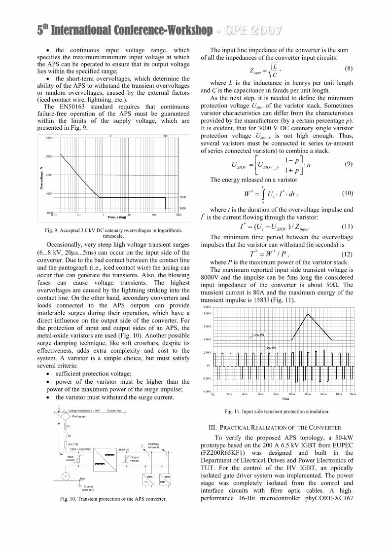
The EN50163 standard requires that continuous failure-free operation of the APS must be guaranteed within the limits of the supply voltage, which are presented in Fig. 9.
0.01 0.1 1 10 100 3500
4000
4500
5000
5500
Time, s (log)
3900
3600
2 300
1000
Ove
rvol
tage
. V
Fig. 9. Accepted 3.0 kV DC catenary overvoltages in logarithmic
timescale.
Occasionally, very steep high voltage transient surges (6...8 kV, 20μs...5ms) can occur on the input side of the converter. Due to the bad contact between the contact line and the pantograph (i.e., iced contact wire) the arcing can occur that can generate the transients. Also, the blowing fuses can cause voltage transients. The highest overvoltages are caused by the lightning striking into the contact line. On the other hand, secondary converters and loads connected to the APS outputs can provide intolerable surges during their operation, which have a direct influence on the output side of the converter. For the protection of input and output sides of an APS, the metal-oxide varistors are used (Fig. 10). Another possible surge damping technique, like soft crowbars, despite its effectiveness, adds extra complexity and cost to the system. A varistor is a simple choice, but must satisfy several criteria:
• sufficient protection voltage; • power of the varistor must be higher than the power of the maximum power of the surge impulse; • the varistor must withstand the surge current.
Pantograph
Contact lineVoltage transients 6 – 8kV
Rin 11Ω
Rail
Ground (zero ref.)
Input varistor
Output varistor
2200 – 4000VDC 350V DC
S1
F1
Switching transients
Fig. 10. Transient protection of the APS converter.
The input line impedance of the converter is the sum of all the impedances of the converter input circuits:
CLZinput = , (8)
where L is the inductance in henrys per unit length and C is the capacitance in farads per unit length.
As the next step, it is needed to define the minimum protection voltage Usiov of the varistor stack. Sometimes varistor characteristics can differ from the characteristics provided by the manufacturer (by a certain percentage p). It is evident, that for 3000 V DC catenary single varistor protection voltage Usiov-v is not high enough. Thus, several varistors must be connected in series (n-amount of series connected varistors) to combine a stack:
nppUU VSIOVSIOV ⋅⎥
⎦
⎤⎢⎣
⎡+−
⋅=11
_ (9)
The energy released on a varistor
, (10) dtIUW t
t
⋅⋅= ∫ *
0
*
where t is the duration of the overvoltage impulse and I* is the current flowing through the varistor: (11) inputSIOVt ZUUI /)(* −=
The minimum time period between the overvoltage impulses that the varistor can withstand (in seconds) is , (12) PWT /** =
where P is the maximum power of the varistor stack. The maximum reported input side transient voltage is
8000V and the impulse can be 5ms long the considered input impedance of the converter is about 50Ω. The transient current is 80A and the maximum energy of the transient impulse is 1583J (Fig. 11).
Time 0s
UDC [V]
UTX [V]
9.0KV
8.0KV
6.0KV
4.0KV
2.0KV
0V
-2.0KV
-4.0KV2ms 4ms 6ms 8ms 10ms 12ms 14ms 16ms 18ms
Fig. 11. Input side transient protection simulation.
III. PRACTICAL REALIZATION OF THE CONVERTER To verify the proposed APS topology, a 50-kW
prototype based on the 200 A 6.5 kV IGBT from EUPEC (FZ200R65KF1) was designed and built in the Department of Electrical Drives and Power Electronics of TUT. For the control of the HV IGBT, an optically isolated gate driver system was implemented. The power stage was completely isolated from the control and interface circuits with fibre optic cables. A high-performance 16-Bit microcontroller phyCORE-XC167
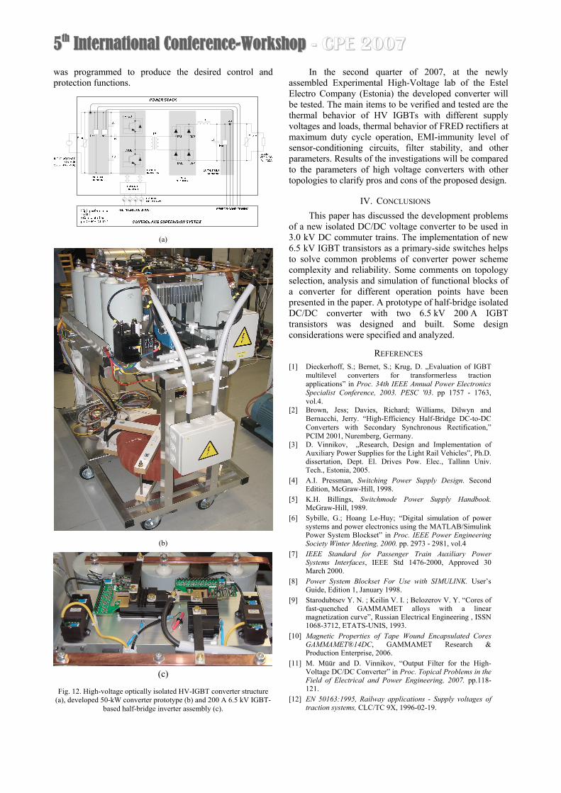
55tthh IInntteerrnnaattiioonnaall CCoonnffeerreennccee--WWoorrkksshhoopp - CPE 2007
was programmed to produce the desired control and protection functions.
(a)
(b)
(c)
Fig. 12. High-voltage optically isolated HV-IGBT converter structure (a), developed 50-kW converter prototype (b) and 200 A 6.5 kV IGBT-
based half-bridge inverter assembly (c).
In the second quarter of 2007, at the newly assembled Experimental High-Voltage lab of the Estel Electro Company (Estonia) the developed converter will be tested. The main items to be verified and tested are the thermal behavior of HV IGBTs with different supply voltages and loads, thermal behavior of FRED rectifiers at maximum duty cycle operation, EMI-immunity level of sensor-conditioning circuits, filter stability, and other parameters. Results of the investigations will be compared to the parameters of high voltage converters with other topologies to clarify pros and cons of the proposed design.
IV. CONCLUSIONS This paper has discussed the development problems
of a new isolated DC/DC voltage converter to be used in 3.0 kV DC commuter trains. The implementation of new 6.5 kV IGBT transistors as a primary-side switches helps to solve common problems of converter power scheme complexity and reliability. Some comments on topology selection, analysis and simulation of functional blocks of a converter for different operation points have been presented in the paper. A prototype of half-bridge isolated DC/DC converter with two 6.5 kV 200 A IGBT transistors was designed and built. Some design considerations were specified and analyzed.
REFERENCES [1] Dieckerhoff, S.; Bernet, S.; Krug, D. „Evaluation of IGBT
multilevel converters for transformerless traction applications” in Proc. 34th IEEE Annual Power Electronics Specialist Conference, 2003. PESC '03. pp 1757 - 1763, vol.4.
[2] Brown, Jess; Davies, Richard; Williams, Dilwyn and Bernacchi, Jerry. “High-Efficiency Half-Bridge DC-to-DC Converters with Secondary Synchronous Rectification,” PCIM 2001, Nuremberg, Germany.
[3] D. Vinnikov, „Research, Design and Implementation of Auxiliary Power Supplies for the Light Rail Vehicles”, Ph.D. dissertation, Dept. El. Drives Pow. Elec., Tallinn Univ. Tech., Estonia, 2005.
[4] A.I. Pressman, Switching Power Supply Design. Second Edition, McGraw-Hill, 1998.
[5] K.H. Billings, Switchmode Power Supply Handbook. McGraw-Hill, 1989.
[6] Sybille, G.; Hoang Le-Huy; “Digital simulation of power systems and power electronics using the MATLAB/Simulink Power System Blockset” in Proc. IEEE Power Engineering Society Winter Meeting, 2000. pp. 2973 - 2981, vol.4
[7] IEEE Standard for Passenger Train Auxiliary Power Systems Interfaces, IEEE Std 1476-2000, Approved 30 March 2000.
[8] Power System Blockset For Use with SIMULINK. User’s Guide, Edition 1, January 1998.
[9] Starodubtsev Y. N. ; Keilin V. I. ; Belozerov V. Y. “Cores of fast-quenched GAMMAMET alloys with a linear magnetization curve”, Russian Electrical Engineering , ISSN 1068-3712, ETATS-UNIS, 1993.
[10] Magnetic Properties of Tape Wound Encapsulated Cores GAMMAMET®14DC, GAMMAMET Research & Production Enterprise, 2006.
[11] M. Müür and D. Vinnikov, “Output Filter for the High-Voltage DC/DC Converter” in Proc. Topical Problems in the Field of Electrical and Power Engineering, 2007. pp.118-121.
[12] EN 50163:1995, Railway applications - Supply voltages of traction systems, CLC/TC 9X, 1996-02-19.