
36-75 Vdc DC/DC converter Output up to 80 A/128 W - Octopart
Upload
independentCategory
view
0download
0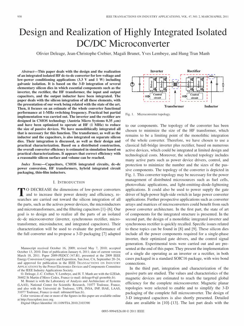
930 IEEE TRANSACTIONS ON INDUSTRY APPLICATIONS, VOL. 47, NO. 2, MARCH/APRIL 2011
Design and Realization of Highly Integrated IsolatedDC/DC Microconverter
Olivier Deleage, Jean-Christophe Crebier, Magali Brunet, Yves Lembeye, and Hung Tran Manh
Abstract—This paper deals with the design and the realizationof an integrated isolated HF dc-to-dc converter for low-voltage andlow-power conditioning applications (3.3 V and 1 W) includinggalvanic isolation. It is based on the 3-D integration of severalelementary silicon dies in which essential components such as theinverter, the rectifier, the HF transformer, the input and outputcapacitors, and the output inductor have been integrated. Thepaper deals with the silicon integration of all these elements, withthe presentation of our work being related with the state of the art.Then, it focuses on an estimate of the whole converter functionalperformance at 1-MHz switching frequency. Practical but partialimplementation was carried out. The inverter and the rectifier aredesigned in CMOS technology (Austria Micro Systems 0.35 μm)and have been optimized to operate at HF (1 MHz) to reducethe size of passive devices. We have monolithically integrated allthat is necessary for this function. The transformer, as well as theinductor and the capacitors, is also integrated on separate silicondies. Their integration is discussed, as well as their design andpractical characterization. Based on a distributed construction,the overall converter efficiency is estimated in simulation based onpractical characterizations. It appears that correct efficiency witha reasonable silicon surface and volume can be reached.
Index Terms—Capacitors, CMOS integrated circuits, dc–dcpower conversion, HF transformers, hybrid integrated circuitpackaging, thin-film inductors.
I. INTRODUCTION
TO DECREASE the dimensions of low-power convertersand to increase their power density and efficiency, re-
searches are carried out toward the silicon integration of allthe parts, such as the actives power devices, the microinductorsand microtransformers, and the filtering capacitors [1]–[6]. Ourgoal is to design and to realize all the parts of an isolateddc–dc microconverter (inverter, synchronous rectifier, micro-transformer, microinductor, and integrated capacitors). Theircharacterization will be used to evaluate the performance ofthe full converter and to propose a 3-D packaging [7] adapted
Manuscript received October 16, 2009; revised May 7, 2010; acceptedOctober 13, 2010. Date of publication January 6, 2011; date of current versionMarch 18, 2011. Paper 2009-PEDCC-347.R1, presented at the 2009 IEEEEnergy Conversion Congress and Exposition, San Jose, CA, September 20–24,and approved for publication in the IEEE TRANSACTIONS ON INDUSTRY
APPLICATIONS by the Power Electronics Devices and Components Committeeof the IEEE Industry Applications Society.
O. Deleage, J.-C. Crebier, Y. Lembeye, and H. T. Manh are with the G2Elab,38402 St Martin d’Hères Cedex, France (e-mail: [email protected]).
M. Brunet is with the Laboratory of Analysis and Architecture of Systems(LAAS), National Center for Scientific Research, 31077 Toulouse, France,and also with the Université de Toulouse, UPS, INSA, INP, ISAE, LAAS,31077 Toulouse, France (e-mail: [email protected]).
Color versions of one or more of the figures in this paper are available onlineat http://ieeexplore.ieee.org.
Digital Object Identifier 10.1109/TIA.2010.2103390
Fig. 1. Microconverter topology.
to our components. The topology of the converter has beenchosen to minimize the size of the HF transformer, whichremains to be a limiting point of the monolithic integrationof the whole converter. Therefore, we have chosen to use aclassical full-bridge inverter plus rectifier, based on numerousactive devices, which could be integrated at limited design andtechnological costs. Moreover, the selected topology includesmany active parts such as power device drivers, control, andprotection to minimize the number and the sizes of the pas-sive components. The topology of the converter is depicted inFig. 1. This converter topology may be necessary for the powermanagement of distributed microsources such as fuel cells,photovoltaic applications, and light-emitting-diode-lighteningapplications. It could also be used to power supply the gatedriver of high-power high-side switch in large power converterapplications. Further prospective applications such as converterarrays and matrices of microconverters could benefit from suchpower converter architecture. In the first part, the state of artof components for the integrated structure is presented. In thesecond part, the design of a monolithic integrated inverter andsynchronous rectifier is quickly recalled. Specific issues relatedto these topics can be found in [8] and [9]. These silicon diesinclude all the power components required for a single-phaseinverter, their optimized gate drivers, and the control signalgeneration. Experimental tests were carried out and are pre-sented at the end of this paper. They present the implementationof a single die operating as an inverter or a rectifier, in bothcases packaged in a standard SOIC16 package, with wire bondconnections.
In the third part, integration and characterization of thepassive parts are studied. The values and characteristics of themagnetic devices are estimated to reach the targeted globalefficiency for the complete microconverter. Magnetic planartopologies were selected to enable and to simplify the 3-Dpackaging of the complete full microconverter. The design of3-D integrated capacitors is also shortly presented. Detaileddata are available in [10]–[13]. The last part deals with the
0093-9994/$26.00 © 2011 IEEE
DELEAGE et al.: DESIGN AND REALIZATION OF HIGHLY INTEGRATED ISOLATED DC/DC MICROCONVERTER 931
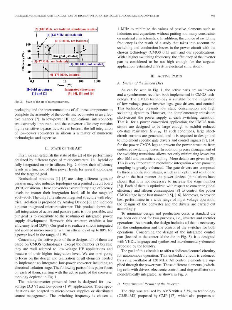
Fig. 2. State of the art of microconverters.
packaging and the interconnections of all these components tocomplete the assembly of the dc–dc microconverter in an effec-tive manner [7]. In low-power HF applications, interconnectsare extremely important, and the converter efficiency remainshighly sensitive to parasitics. As can be seen, the full integrationof low-power converters in silicon is a matter of numeroustechnologies and expertise.
II. STATE OF THE ART
First, we can establish the state of the art of the performanceobtained by different types of microconverters, i.e., hybrid orfully integrated on or in silicon. Fig. 2 shows their efficiencylevels as a function of their power levels for several topologiesand the targeted goal.
Nonisolated structures [1]–[5] are using different types ofpassive magnetic inductor topologies on a printed circuit board(PCB) or silicon. These converters exhibit fairly high efficiencylevels no matter their integration level, all in the range of80%–90%. The only fully silicon integrated structure with elec-trical isolation is proposed by Analog Device [6] and includesa planar integrated microtransformer. This product shows thatfull integration of active and passive parts is now possible, andour goal is to contribute to the roadmap of integrated powersupply development. However, this structure exhibits a lowefficiency level (33%). Our goal is to realize a silicon integratedand isolated microconverter with an efficiency of up to 80% fora power level in the range of 1 W.
Concerning the active parts of these designs, all of them arebased on CMOS technologies (except the number 2) becausethey are well adapted to low-voltage HF applications andbecause of their higher integration level. We are now goingto focus on the design and realization of all elements neededto implement an integrated low-power converter including anelectrical isolation stage. The following parts of this paper focuson each of them, starting with the active parts of the convertertopology depicted in Fig. 1.
The microconverter presented here is designed for low-voltage (3.3 V) and low-power (1 W) applications. These spec-ifications are adapted to micro-power supplies or distributedsource management. The switching frequency is chosen at
1 MHz to minimize the values of passive elements such asinductors and capacitors without putting too many constraintson material characteristics. In addition, the choice of switchingfrequency is the result of a study that takes into account theswitching and conduction losses in the power circuit with thechosen technology (CMOS 0.35 μm) and our specifications.With a higher switching frequency, the efficiency of the inverterpart is considered to be not high enough for the targetedapplication (estimated at 98% in electrical simulation).
III. ACTIVE PARTS
A. Design of the Silicon Dies
As can be seen in Fig. 1, the active parts are an inverterand a synchronous rectifier, both implemented in CMOS tech-nology. The CMOS technology is suitable for the integrationof low-voltage power inverter legs, gate drivers, and control.This technology presents low static consumption and highswitching dynamics. However, the complementary transistorsshort-circuit the power supply at each switching transition.That is, for a power conversion application, the CMOS tran-sistors are designed to be large enough to exhibit reducedON-state resistance RDSON. In such conditions, large short-circuit currents are generated, and it is required to design andto implement specific gate drivers and control signals [9], [14]for the power CMOS legs to prevent the power structure fromundesired switching losses. In addition, precise management ofthe switching transitions allows not only minimizing losses butalso EMI and parasitic coupling. More details are given in [8].This is very important in monolithic integration where parasiticcoupling is greatly enhanced. The gate drivers are composedby three amplification stages, which is an optimized solution todrive in the best manner the power devices (simulations haveshown that it is not necessary to increase the stage number[8]). Each of them is optimized with respect to converter globalefficiency and silicon consumption [8] to control the powerCMOS stage in the best manner [15], [16]. Moreover, to providebest performance in a wide range of input voltage operation,the designs of the converter and the drivers are carried outaccordingly.
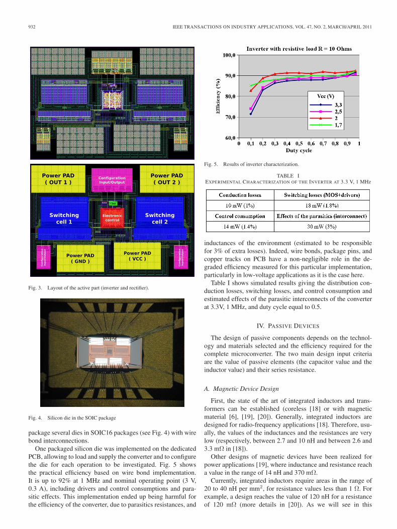
To minimize design and production costs, a standard diehas been designed for two purposes, i.e., inverter and rectifieroperations. As a result, the design includes all that is necessaryfor the configuration and the control of the switches for bothoperations. Concerning the design of the integrated controlpart (located at the center of the die in Fig. 3), it is designedwith VHDL language and synthesized into elementary elementsproposed by the foundry.
The goal of this circuit is to offer a dedicated control circuitryfor autonomous operation. This embedded circuit is cadencedby a ring oscillator at 120 MHz. All control elements are sup-plied through the power part. These different elements (switch-ing cells with drivers, electronic control, and ring oscillator) aremonolithically integrated, as shown in Fig. 3.
B. Experimental Results of the Inverter
The chip was realized by AMS with a 3.35-μm technology(C35B4M3) proposed by CMP [17], which also proposes to
932 IEEE TRANSACTIONS ON INDUSTRY APPLICATIONS, VOL. 47, NO. 2, MARCH/APRIL 2011
Fig. 3. Layout of the active part (inverter and rectifier).
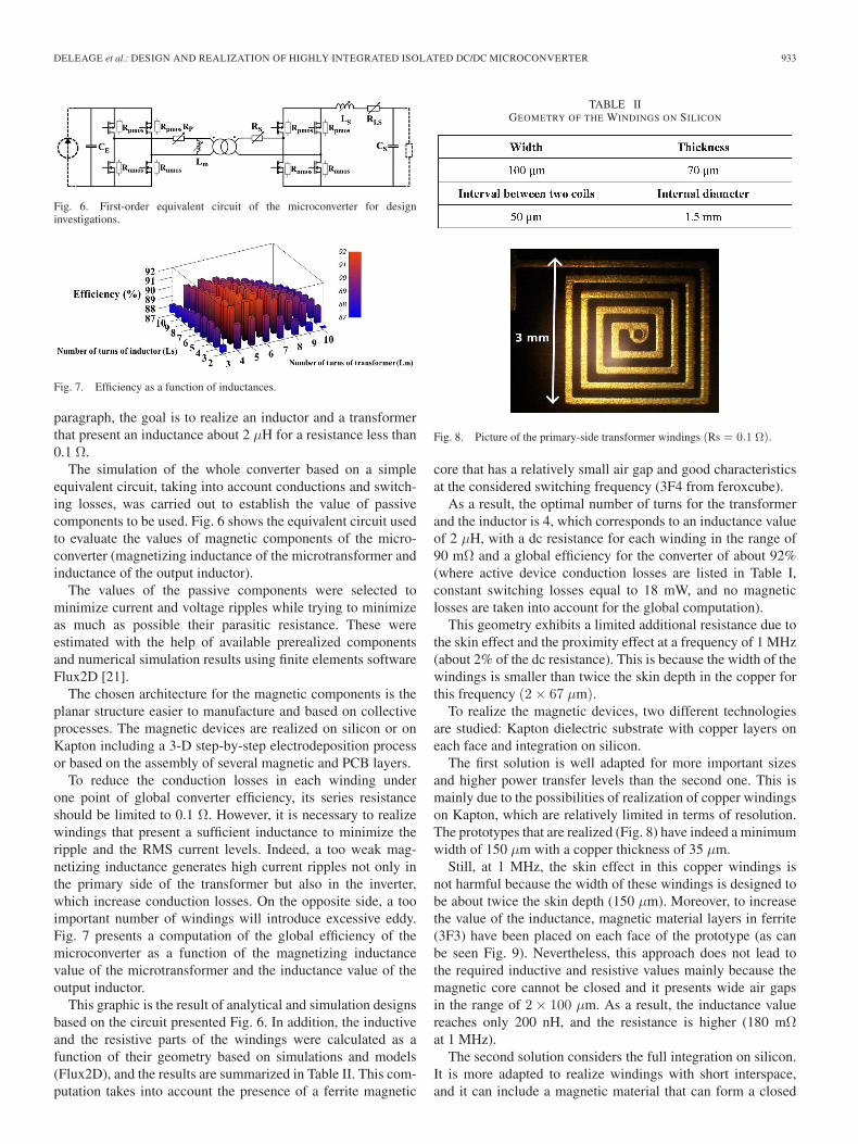
Fig. 4. Silicon die in the SOIC package
package several dies in SOIC16 packages (see Fig. 4) with wirebond interconnections.
One packaged silicon die was implemented on the dedicatedPCB, allowing to load and supply the converter and to configurethe die for each operation to be investigated. Fig. 5 showsthe practical efficiency based on wire bond implementation.It is up to 92% at 1 MHz and nominal operating point (3 V,0.3 A), including drivers and control consumptions and para-sitic effects. This implementation ended up being harmful forthe efficiency of the converter, due to parasitics resistances, and
Fig. 5. Results of inverter characterization.
TABLE IEXPERIMENTAL CHARACTERIZATION OF THE INVERTER AT 3.3 V, 1 MHz
inductances of the environment (estimated to be responsiblefor 3% of extra losses). Indeed, wire bonds, package pins, andcopper tracks on PCB have a non-negligible role in the de-graded efficiency measured for this particular implementation,particularly in low-voltage applications as it is the case here.
Table I shows simulated results giving the distribution con-duction losses, switching losses, and control consumption andestimated effects of the parasitic interconnects of the converterat 3.3V, 1 MHz, and duty cycle equal to 0.5.
IV. PASSIVE DEVICES
The design of passive components depends on the technol-ogy and materials selected and the efficiency required for thecomplete microconverter. The two main design input criteriaare the value of passive elements (the capacitor value and theinductor value) and their series resistance.
A. Magnetic Device Design
First, the state of the art of integrated inductors and trans-formers can be established (coreless [18] or with magneticmaterial [6], [19], [20]). Generally, integrated inductors aredesigned for radio-frequency applications [18]. Therefore, usu-ally, the values of the inductances and the resistances are verylow (respectively, between 2.7 and 10 nH and between 2.6 and3.3 mΩ in [18]).
Other designs of magnetic devices have been realized forpower applications [19], where inductance and resistance reacha value in the range of 14 nH and 370 mΩ.
Currently, integrated inductors require areas in the range of20 to 40 nH per mm2, for resistance values less than 1 Ω. Forexample, a design reaches the value of 120 nH for a resistanceof 120 mΩ (more details in [20]). As we will see in this
DELEAGE et al.: DESIGN AND REALIZATION OF HIGHLY INTEGRATED ISOLATED DC/DC MICROCONVERTER 933
Fig. 6. First-order equivalent circuit of the microconverter for designinvestigations.
Fig. 7. Efficiency as a function of inductances.
paragraph, the goal is to realize an inductor and a transformerthat present an inductance about 2 μH for a resistance less than0.1 Ω.
The simulation of the whole converter based on a simpleequivalent circuit, taking into account conductions and switch-ing losses, was carried out to establish the value of passivecomponents to be used. Fig. 6 shows the equivalent circuit usedto evaluate the values of magnetic components of the micro-converter (magnetizing inductance of the microtransformer andinductance of the output inductor).
The values of the passive components were selected tominimize current and voltage ripples while trying to minimizeas much as possible their parasitic resistance. These wereestimated with the help of available prerealized componentsand numerical simulation results using finite elements softwareFlux2D [21].
The chosen architecture for the magnetic components is theplanar structure easier to manufacture and based on collectiveprocesses. The magnetic devices are realized on silicon or onKapton including a 3-D step-by-step electrodeposition processor based on the assembly of several magnetic and PCB layers.
To reduce the conduction losses in each winding underone point of global converter efficiency, its series resistanceshould be limited to 0.1 Ω. However, it is necessary to realizewindings that present a sufficient inductance to minimize theripple and the RMS current levels. Indeed, a too weak mag-netizing inductance generates high current ripples not only inthe primary side of the transformer but also in the inverter,which increase conduction losses. On the opposite side, a tooimportant number of windings will introduce excessive eddy.Fig. 7 presents a computation of the global efficiency of themicroconverter as a function of the magnetizing inductancevalue of the microtransformer and the inductance value of theoutput inductor.
This graphic is the result of analytical and simulation designsbased on the circuit presented Fig. 6. In addition, the inductiveand the resistive parts of the windings were calculated as afunction of their geometry based on simulations and models(Flux2D), and the results are summarized in Table II. This com-putation takes into account the presence of a ferrite magnetic
TABLE IIGEOMETRY OF THE WINDINGS ON SILICON
Fig. 8. Picture of the primary-side transformer windings (Rs = 0.1 Ω).
core that has a relatively small air gap and good characteristicsat the considered switching frequency (3F4 from feroxcube).
As a result, the optimal number of turns for the transformerand the inductor is 4, which corresponds to an inductance valueof 2 μH, with a dc resistance for each winding in the range of90 mΩ and a global efficiency for the converter of about 92%(where active device conduction losses are listed in Table I,constant switching losses equal to 18 mW, and no magneticlosses are taken into account for the global computation).
This geometry exhibits a limited additional resistance due tothe skin effect and the proximity effect at a frequency of 1 MHz(about 2% of the dc resistance). This is because the width of thewindings is smaller than twice the skin depth in the copper forthis frequency (2 × 67 μm).
To realize the magnetic devices, two different technologiesare studied: Kapton dielectric substrate with copper layers oneach face and integration on silicon.
The first solution is well adapted for more important sizesand higher power transfer levels than the second one. This ismainly due to the possibilities of realization of copper windingson Kapton, which are relatively limited in terms of resolution.The prototypes that are realized (Fig. 8) have indeed a minimumwidth of 150 μm with a copper thickness of 35 μm.
Still, at 1 MHz, the skin effect in this copper windings isnot harmful because the width of these windings is designed tobe about twice the skin depth (150 μm). Moreover, to increasethe value of the inductance, magnetic material layers in ferrite(3F3) have been placed on each face of the prototype (as canbe seen Fig. 9). Nevertheless, this approach does not lead tothe required inductive and resistive values mainly because themagnetic core cannot be closed and it presents wide air gapsin the range of 2 × 100 μm. As a result, the inductance valuereaches only 200 nH, and the resistance is higher (180 mΩat 1 MHz).
The second solution considers the full integration on silicon.It is more adapted to realize windings with short interspace,and it can include a magnetic material that can form a closed

934 IEEE TRANSACTIONS ON INDUSTRY APPLICATIONS, VOL. 47, NO. 2, MARCH/APRIL 2011
Fig. 9. Transformer with magnetic circuit.
Fig. 10. Top view and cut view of a 1-μH inductor integrated on silicon.
Fig. 11. Proposed topology of the transformer on silicon and magnetic core.
magnetic core. If physical vapor deposition techniques (sput-tering, evaporation) are considered for the conductive and mag-netic layers deposition, the thickness will be limited. Therefore,the realization of the conductors and the magnetic core wasbased on the electrodeposition technique that allows depositingthick layers in a reasonable time and cost. A CoNiFe elec-troplating bath was developed [31] that gave the followingcharacteristics for the magnetic core layer: a saturation fluxdensity (Bsat) of 2.2 T, a coercive field (Hc) of 24 Oe, and arelative permeability of 250. An inductor (7 mm × 3 mm) with46-μm-thick copper conductors and 35-μm-thick laminatedmagnetic core was fully processed on silicon (Fig. 10). Itscharacterization gave the following values: 1 μH up to 1 MHzand a dc resistance of 1.2 Ω. Future components should presenta thicker copper conductor for decreasing the conductive losses.
The main drawback of this topology of inductor is the air gapbetween the two layers of electrodeposed NiFe, which reducesthe reachable value of inductance.
To realize an integrated microtransformer with a magneticcore with a minimum air gap and using optimized materials,the topology presented Fig. 11 is proposed.
This solution is based on the deposition of the two windingsof the microtransformer on a thin layer of SiO2 (1.3 μm) ob-tained from the thermal oxidation of a regular silicon substrate.Windings were realized by electrodeposition of copper from athin seed layer of Ti/Au obtained by evaporation (10 nm of Tiand 100 nm of Au).
The two holes on the center of the windings were realizedby deep reactive ion etching (DRIE). During this step, a trenchwas realized in the silicon substrate and between the two holes
Fig. 12. Details of the proposed topology of transformer.
Fig. 13. Prototype of the microtransformer on silicon and magnetic core.
(Fig. 12). It allows reducing the induced current in the substrate,which would otherwise generate extra losses. This allows im-plementing this technology on any substrate at a reasonablecost. After the realization of the holes and electrodepositionof the windings, the cores can be added by collective processon the whole wafer. For the prototype, the magnetic core ismachined in ferrite material.
Fig. 13 shows a picture of the prototype realized.The first realized specimen presents a nonhomogeneous and
a smaller thickness of copper, due to a problem during the elec-trodeposition process. In consequence, the windings present ahigher resistance than expected (0.7 Ω instead of 0.2 Ω with35 μm of electrodeposited copper). The magnetic characteriza-tion has been carried out at first with the inductor componentwhich is similar to the microtransformer but with only onewinding. Its inductance value is about 70 nH without mag-netic core (34 nH expected), and with the magnetic core, theinductance reaches the value of 1.6 μH (3 μH expected). Thedifference between measured and expected inductances is dueto the difficulties to realize the measures in good conditions andto estimate the air gap in the magnetic core, which depends verymuch on the roughness of the ferrite material.
Future work will focus on the improvement of the electrode-position of copper to reach thicker windings and on a goodexperimental implementation for the measurements.
B. Capacitor Design
For realizing output filters for dc–dc converters with highperformance, i.e., high power density and high efficiency,integrated capacitors should present high capacitance densitycombined with low series resistance (for minimum loss). Highcapacitance densities may be reached by decreasing the di-electric thickness, increasing the surface area or by using adielectric with high permittivity (k). High-k materials havewidely been investigated in microelectronics as a replacementfor silicon oxide in transistors, and they appear as well for
DELEAGE et al.: DESIGN AND REALIZATION OF HIGHLY INTEGRATED ISOLATED DC/DC MICROCONVERTER 935
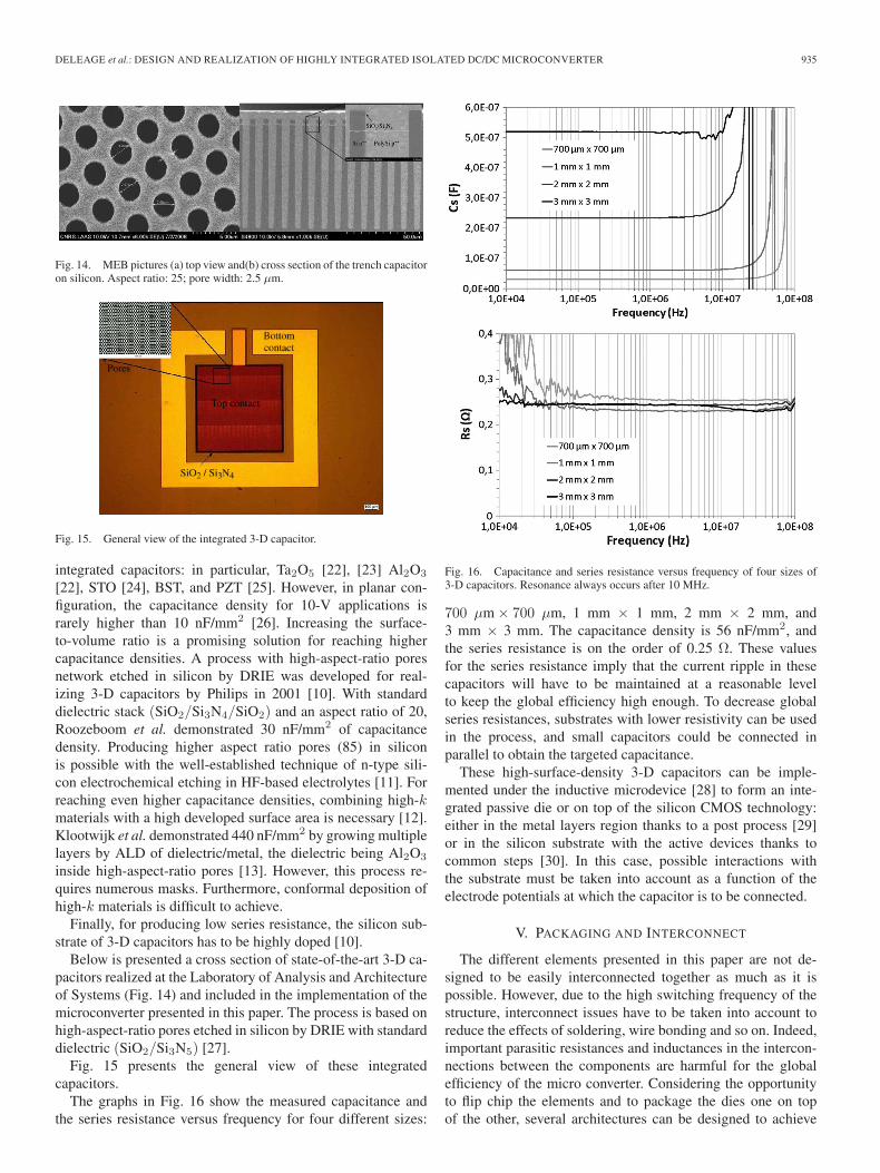
Fig. 14. MEB pictures (a) top view and(b) cross section of the trench capacitoron silicon. Aspect ratio: 25; pore width: 2.5 μm.
Fig. 15. General view of the integrated 3-D capacitor.
integrated capacitors: in particular, Ta2O5 [22], [23] Al2O3
[22], STO [24], BST, and PZT [25]. However, in planar con-figuration, the capacitance density for 10-V applications israrely higher than 10 nF/mm2 [26]. Increasing the surface-to-volume ratio is a promising solution for reaching highercapacitance densities. A process with high-aspect-ratio poresnetwork etched in silicon by DRIE was developed for real-izing 3-D capacitors by Philips in 2001 [10]. With standarddielectric stack (SiO2/Si3N4/SiO2) and an aspect ratio of 20,Roozeboom et al. demonstrated 30 nF/mm2 of capacitancedensity. Producing higher aspect ratio pores (85) in siliconis possible with the well-established technique of n-type sili-con electrochemical etching in HF-based electrolytes [11]. Forreaching even higher capacitance densities, combining high-kmaterials with a high developed surface area is necessary [12].Klootwijk et al. demonstrated 440 nF/mm2 by growing multiplelayers by ALD of dielectric/metal, the dielectric being Al2O3
inside high-aspect-ratio pores [13]. However, this process re-quires numerous masks. Furthermore, conformal deposition ofhigh-k materials is difficult to achieve.
Finally, for producing low series resistance, the silicon sub-strate of 3-D capacitors has to be highly doped [10].
Below is presented a cross section of state-of-the-art 3-D ca-pacitors realized at the Laboratory of Analysis and Architectureof Systems (Fig. 14) and included in the implementation of themicroconverter presented in this paper. The process is based onhigh-aspect-ratio pores etched in silicon by DRIE with standarddielectric (SiO2/Si3N5) [27].
Fig. 15 presents the general view of these integratedcapacitors.
The graphs in Fig. 16 show the measured capacitance andthe series resistance versus frequency for four different sizes:
Fig. 16. Capacitance and series resistance versus frequency of four sizes of3-D capacitors. Resonance always occurs after 10 MHz.
700 μm × 700 μm, 1 mm × 1 mm, 2 mm × 2 mm, and3 mm × 3 mm. The capacitance density is 56 nF/mm2, andthe series resistance is on the order of 0.25 Ω. These valuesfor the series resistance imply that the current ripple in thesecapacitors will have to be maintained at a reasonable levelto keep the global efficiency high enough. To decrease globalseries resistances, substrates with lower resistivity can be usedin the process, and small capacitors could be connected inparallel to obtain the targeted capacitance.
These high-surface-density 3-D capacitors can be imple-mented under the inductive microdevice [28] to form an inte-grated passive die or on top of the silicon CMOS technology:either in the metal layers region thanks to a post process [29]or in the silicon substrate with the active devices thanks tocommon steps [30]. In this case, possible interactions withthe substrate must be taken into account as a function of theelectrode potentials at which the capacitor is to be connected.
V. PACKAGING AND INTERCONNECT
The different elements presented in this paper are not de-signed to be easily interconnected together as much as it ispossible. However, due to the high switching frequency of thestructure, interconnect issues have to be taken into account toreduce the effects of soldering, wire bonding and so on. Indeed,important parasitic resistances and inductances in the intercon-nections between the components are harmful for the globalefficiency of the micro converter. Considering the opportunityto flip chip the elements and to package the dies one on topof the other, several architectures can be designed to achieve
936 IEEE TRANSACTIONS ON INDUSTRY APPLICATIONS, VOL. 47, NO. 2, MARCH/APRIL 2011
Fig. 17. Example of microconverter packaging.
Fig. 18. Microconverter using active parts with trench capacitors and micro-transformer with closed magnetic core in ferrite.
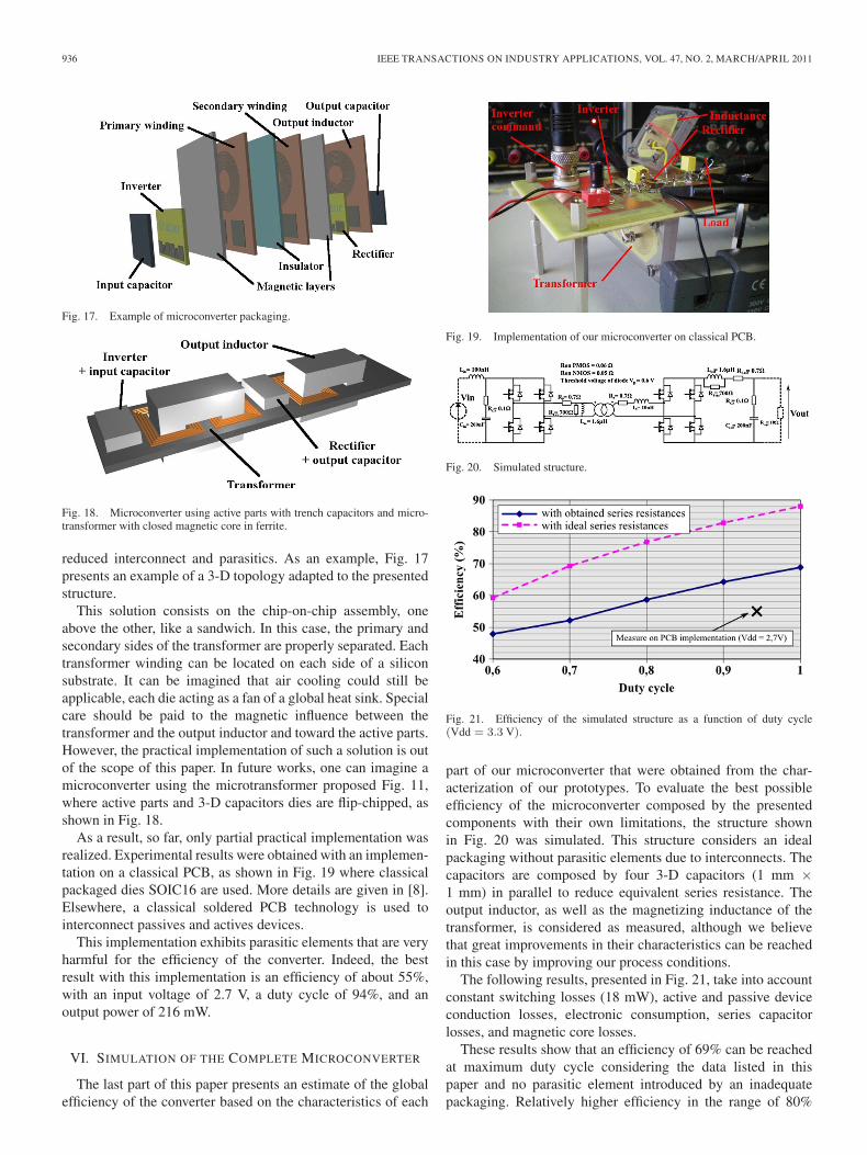
reduced interconnect and parasitics. As an example, Fig. 17presents an example of a 3-D topology adapted to the presentedstructure.
This solution consists on the chip-on-chip assembly, oneabove the other, like a sandwich. In this case, the primary andsecondary sides of the transformer are properly separated. Eachtransformer winding can be located on each side of a siliconsubstrate. It can be imagined that air cooling could still beapplicable, each die acting as a fan of a global heat sink. Specialcare should be paid to the magnetic influence between thetransformer and the output inductor and toward the active parts.However, the practical implementation of such a solution is outof the scope of this paper. In future works, one can imagine amicroconverter using the microtransformer proposed Fig. 11,where active parts and 3-D capacitors dies are flip-chipped, asshown in Fig. 18.
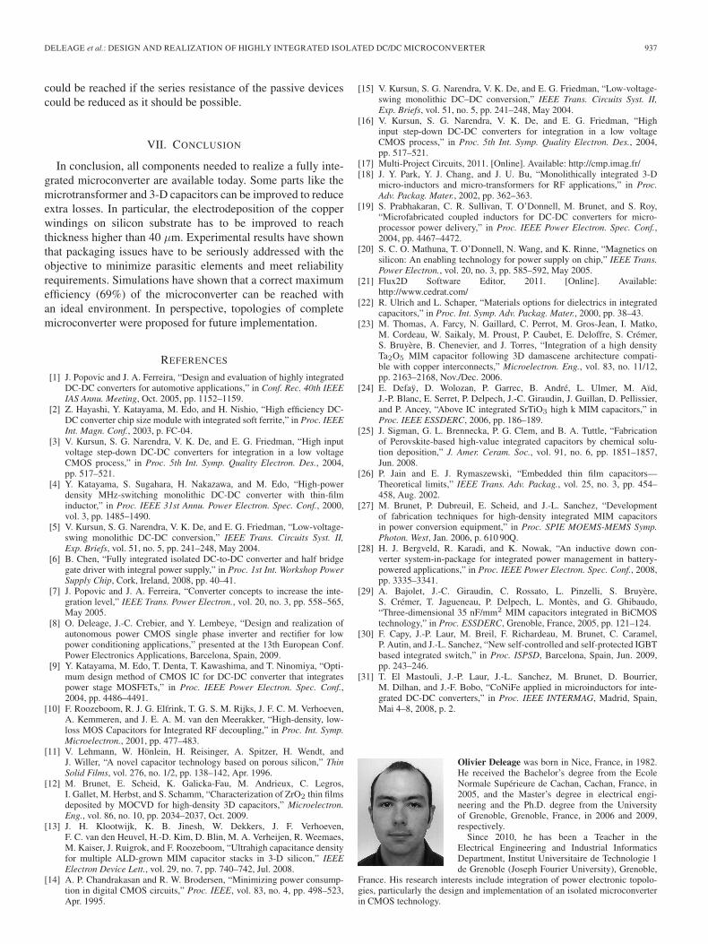
As a result, so far, only partial practical implementation wasrealized. Experimental results were obtained with an implemen-tation on a classical PCB, as shown in Fig. 19 where classicalpackaged dies SOIC16 are used. More details are given in [8].Elsewhere, a classical soldered PCB technology is used tointerconnect passives and actives devices.
This implementation exhibits parasitic elements that are veryharmful for the efficiency of the converter. Indeed, the bestresult with this implementation is an efficiency of about 55%,with an input voltage of 2.7 V, a duty cycle of 94%, and anoutput power of 216 mW.
VI. SIMULATION OF THE COMPLETE MICROCONVERTER
The last part of this paper presents an estimate of the globalefficiency of the converter based on the characteristics of each
Fig. 19. Implementation of our microconverter on classical PCB.
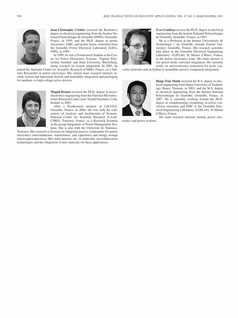
Fig. 20. Simulated structure.
Fig. 21. Efficiency of the simulated structure as a function of duty cycle(Vdd = 3.3 V).
part of our microconverter that were obtained from the char-acterization of our prototypes. To evaluate the best possibleefficiency of the microconverter composed by the presentedcomponents with their own limitations, the structure shownin Fig. 20 was simulated. This structure considers an idealpackaging without parasitic elements due to interconnects. Thecapacitors are composed by four 3-D capacitors (1 mm ×1 mm) in parallel to reduce equivalent series resistance. Theoutput inductor, as well as the magnetizing inductance of thetransformer, is considered as measured, although we believethat great improvements in their characteristics can be reachedin this case by improving our process conditions.
The following results, presented in Fig. 21, take into accountconstant switching losses (18 mW), active and passive deviceconduction losses, electronic consumption, series capacitorlosses, and magnetic core losses.
These results show that an efficiency of 69% can be reachedat maximum duty cycle considering the data listed in thispaper and no parasitic element introduced by an inadequatepackaging. Relatively higher efficiency in the range of 80%
DELEAGE et al.: DESIGN AND REALIZATION OF HIGHLY INTEGRATED ISOLATED DC/DC MICROCONVERTER 937
could be reached if the series resistance of the passive devicescould be reduced as it should be possible.
VII. CONCLUSION
In conclusion, all components needed to realize a fully inte-grated microconverter are available today. Some parts like themicrotransformer and 3-D capacitors can be improved to reduceextra losses. In particular, the electrodeposition of the copperwindings on silicon substrate has to be improved to reachthickness higher than 40 μm. Experimental results have shownthat packaging issues have to be seriously addressed with theobjective to minimize parasitic elements and meet reliabilityrequirements. Simulations have shown that a correct maximumefficiency (69%) of the microconverter can be reached withan ideal environment. In perspective, topologies of completemicroconverter were proposed for future implementation.
REFERENCES
[1] J. Popovic and J. A. Ferreira, “Design and evaluation of highly integratedDC-DC converters for automotive applications,” in Conf. Rec. 40th IEEEIAS Annu. Meeting, Oct. 2005, pp. 1152–1159.
[2] Z. Hayashi, Y. Katayama, M. Edo, and H. Nishio, “High efficiency DC-DC converter chip size module with integrated soft ferrite,” in Proc. IEEEInt. Magn. Conf., 2003, p. FC-04.
[3] V. Kursun, S. G. Narendra, V. K. De, and E. G. Friedman, “High inputvoltage step-down DC-DC converters for integration in a low voltageCMOS process,” in Proc. 5th Int. Symp. Quality Electron. Des., 2004,pp. 517–521.
[4] Y. Katayama, S. Sugahara, H. Nakazawa, and M. Edo, “High-powerdensity MHz-switching monolithic DC-DC converter with thin-filminductor,” in Proc. IEEE 31st Annu. Power Electron. Spec. Conf., 2000,vol. 3, pp. 1485–1490.
[5] V. Kursun, S. G. Narendra, V. K. De, and E. G. Friedman, “Low-voltage-swing monolithic DC-DC conversion,” IEEE Trans. Circuits Syst. II,Exp. Briefs, vol. 51, no. 5, pp. 241–248, May 2004.
[6] B. Chen, “Fully integrated isolated DC-to-DC converter and half bridgegate driver with integral power supply,” in Proc. 1st Int. Workshop PowerSupply Chip, Cork, Ireland, 2008, pp. 40–41.
[7] J. Popovic and J. A. Ferreira, “Converter concepts to increase the inte-gration level,” IEEE Trans. Power Electron., vol. 20, no. 3, pp. 558–565,May 2005.
[8] O. Deleage, J.-C. Crebier, and Y. Lembeye, “Design and realization ofautonomous power CMOS single phase inverter and rectifier for lowpower conditioning applications,” presented at the 13th European Conf.Power Electronics Applications, Barcelona, Spain, 2009.
[9] Y. Katayama, M. Edo, T. Denta, T. Kawashima, and T. Ninomiya, “Opti-mum design method of CMOS IC for DC-DC converter that integratespower stage MOSFETs,” in Proc. IEEE Power Electron. Spec. Conf.,2004, pp. 4486–4491.
[10] F. Roozeboom, R. J. G. Elfrink, T. G. S. M. Rijks, J. F. C. M. Verhoeven,A. Kemmeren, and J. E. A. M. van den Meerakker, “High-density, low-loss MOS Capacitors for Integrated RF decoupling,” in Proc. Int. Symp.Microelectron., 2001, pp. 477–483.
[11] V. Lehmann, W. Hönlein, H. Reisinger, A. Spitzer, H. Wendt, andJ. Willer, “A novel capacitor technology based on porous silicon,” ThinSolid Films, vol. 276, no. 1/2, pp. 138–142, Apr. 1996.
[12] M. Brunet, E. Scheid, K. Galicka-Fau, M. Andrieux, C. Legros,I. Gallet, M. Herbst, and S. Schamm, “Characterization of ZrO2 thin filmsdeposited by MOCVD for high-density 3D capacitors,” Microelectron.Eng., vol. 86, no. 10, pp. 2034–2037, Oct. 2009.
[13] J. H. Klootwijk, K. B. Jinesh, W. Dekkers, J. F. Verhoeven,F. C. van den Heuvel, H.-D. Kim, D. Blin, M. A. Verheijen, R. Weemaes,M. Kaiser, J. Ruigrok, and F. Roozeboom, “Ultrahigh capacitance densityfor multiple ALD-grown MIM capacitor stacks in 3-D silicon,” IEEEElectron Device Lett., vol. 29, no. 7, pp. 740–742, Jul. 2008.
[14] A. P. Chandrakasan and R. W. Brodersen, “Minimizing power consump-tion in digital CMOS circuits,” Proc. IEEE, vol. 83, no. 4, pp. 498–523,Apr. 1995.
[15] V. Kursun, S. G. Narendra, V. K. De, and E. G. Friedman, “Low-voltage-swing monolithic DC–DC conversion,” IEEE Trans. Circuits Syst. II,Exp. Briefs, vol. 51, no. 5, pp. 241–248, May 2004.
[16] V. Kursun, S. G. Narendra, V. K. De, and E. G. Friedman, “Highinput step-down DC-DC converters for integration in a low voltageCMOS process,” in Proc. 5th Int. Symp. Quality Electron. Des., 2004,pp. 517–521.
[17] Multi-Project Circuits, 2011. [Online]. Available: http://cmp.imag.fr/[18] J. Y. Park, Y. J. Chang, and J. U. Bu, “Monolithically integrated 3-D
micro-inductors and micro-transformers for RF applications,” in Proc.Adv. Packag. Mater., 2002, pp. 362–363.
[19] S. Prabhakaran, C. R. Sullivan, T. O’Donnell, M. Brunet, and S. Roy,“Microfabricated coupled inductors for DC-DC converters for micro-processor power delivery,” in Proc. IEEE Power Electron. Spec. Conf.,2004, pp. 4467–4472.
[20] S. C. O. Mathuna, T. O’Donnell, N. Wang, and K. Rinne, “Magnetics onsilicon: An enabling technology for power supply on chip,” IEEE Trans.Power Electron., vol. 20, no. 3, pp. 585–592, May 2005.
[21] Flux2D Software Editor, 2011. [Online]. Available:http://www.cedrat.com/
[22] R. Ulrich and L. Schaper, “Materials options for dielectrics in integratedcapacitors,” in Proc. Int. Symp. Adv. Packag. Mater., 2000, pp. 38–43.
[23] M. Thomas, A. Farcy, N. Gaillard, C. Perrot, M. Gros-Jean, I. Matko,M. Cordeau, W. Saikaly, M. Proust, P. Caubet, E. Deloffre, S. Crémer,S. Bruyère, B. Chenevier, and J. Torres, “Integration of a high densityTa2O5 MIM capacitor following 3D damascene architecture compati-ble with copper interconnects,” Microelectron. Eng., vol. 83, no. 11/12,pp. 2163–2168, Nov./Dec. 2006.
[24] E. Defaÿ, D. Wolozan, P. Garrec, B. André, L. Ulmer, M. Aïd,J.-P. Blanc, E. Serret, P. Delpech, J.-C. Giraudin, J. Guillan, D. Pellissier,and P. Ancey, “Above IC integrated SrTiO3 high k MIM capacitors,” inProc. IEEE ESSDERC, 2006, pp. 186–189.
[25] J. Sigman, G. L. Brennecka, P. G. Clem, and B. A. Tuttle, “Fabricationof Perovskite-based high-value integrated capacitors by chemical solu-tion deposition,” J. Amer. Ceram. Soc., vol. 91, no. 6, pp. 1851–1857,Jun. 2008.
[26] P. Jain and E. J. Rymaszewski, “Embedded thin film capacitors—Theoretical limits,” IEEE Trans. Adv. Packag., vol. 25, no. 3, pp. 454–458, Aug. 2002.
[27] M. Brunet, P. Dubreuil, E. Scheid, and J.-L. Sanchez, “Developmentof fabrication techniques for high-density integrated MIM capacitorsin power conversion equipment,” in Proc. SPIE MOEMS-MEMS Symp.Photon. West, Jan. 2006, p. 610 90Q.
[28] H. J. Bergveld, R. Karadi, and K. Nowak, “An inductive down con-verter system-in-package for integrated power management in battery-powered applications,” in Proc. IEEE Power Electron. Spec. Conf., 2008,pp. 3335–3341.
[29] A. Bajolet, J.-C. Giraudin, C. Rossato, L. Pinzelli, S. Bruyère,S. Crémer, T. Jagueneau, P. Delpech, L. Montès, and G. Ghibaudo,“Three-dimensional 35 nF/mm2 MIM capacitors integrated in BiCMOStechnology,” in Proc. ESSDERC, Grenoble, France, 2005, pp. 121–124.
[30] F. Capy, J.-P. Laur, M. Breil, F. Richardeau, M. Brunet, C. Caramel,P. Autin, and J.-L. Sanchez, “New self-controlled and self-protected IGBTbased integrated switch,” in Proc. ISPSD, Barcelona, Spain, Jun. 2009,pp. 243–246.
[31] T. El Mastouli, J.-P. Laur, J.-L. Sanchez, M. Brunet, D. Bourrier,M. Dilhan, and J.-F. Bobo, “CoNiFe applied in microinductors for inte-grated DC-DC converters,” in Proc. IEEE INTERMAG, Madrid, Spain,Mai 4–8, 2008, p. 2.
Olivier Deleage was born in Nice, France, in 1982.He received the Bachelor’s degree from the EcoleNormale Supérieure de Cachan, Cachan, France, in2005, and the Master’s degree in electrical engi-neering and the Ph.D. degree from the Universityof Grenoble, Grenoble, France, in 2006 and 2009,respectively.
Since 2010, he has been a Teacher in theElectrical Engineering and Industrial InformaticsDepartment, Institut Universitaire de Technologie 1de Grenoble (Joseph Fourier University), Grenoble,
France. His research interests include integration of power electronic topolo-gies, particularly the design and implementation of an isolated microconverterin CMOS technology.
938 IEEE TRANSACTIONS ON INDUSTRY APPLICATIONS, VOL. 47, NO. 2, MARCH/APRIL 2011
Jean-Christophe Crebier received the Bachelor’sdegree in electrical engineering from the Institut Na-tional Polytechnique de Grenoble (INPG), Grenoble,France, in 1995, and the Ph.D. degree in powerelectronics, EMC, and power factor correction fromthe Grenoble Power Electrical Laboratory (LEG),INPG, in 1999.
In 1999, he was a Postdoctoral Student at the Cen-ter for Power Electronics Systems, Virginia Poly-technic Institute and State University, Blacksburg,doing research on system integration. In 2001, he
joined the National Center for Scientific Research (CNRS), France, as a full-time Researcher in power electronics. His current main research interests in-clude system and functional, hybrid, and monolithic integration and packagingfor medium- to high-voltage active devices.
Magali Brunet received the Ph.D. degree in micro-electronics engineering from the National Microelec-tronic Research Centre (now Tyndall Institute), Cork,Ireland, in 2003.
After a Postdoctoral position at Leti-CEA,Grenoble, France, in 2004, she was with the Lab-oratory of Analysis and Architecture of Systems,National Center for Scientific Research (LAAS-CNRS), Toulouse, France, as a Research Scientistin the group Integration of Power Management Sys-tems. She is also with the Université de Toulouse,
Toulouse. Her research is focused on integrated passive components for powerelectronics (microinductors, transformers, and capacitors) and energy storage(microsupercapacitors). Her main interests are, in particular, microfabricationtechnologies and the integration of new materials for these applications.
Yves Lembeye receive the Ph.D. degree in electricalengineering from the Institut National Polytechniquede Grenoble, Grenoble, France, in 1997.
He is a Professor at the Institut Universitaire deTechnologie 1 de Grenoble (Joseph Fourier Uni-versity), Grenoble, France. His research activitiestake place in the Grenoble Electrical EngineeringLaboratory (G2ELab), St Martin d’Hères, France,in the power electronics team. His main interest islow-power dc/dc converter integration. He currentlyworks on microconverter realization for dc/dc con-
verter networks and on hybrid or monolithic passive component integration.
Hung Tran Manh received the B.S. degree in elec-trical engineering from Hanoi University of Technol-ogy, Hanoi, Vietnam, in 2001, and the M.S. degreein electrical engineering from the Institut NationalPolytechnique de Grenoble, Grenoble, France, in2007. He is currently working toward the Ph.D.degree in complementary technology in power con-version structures and EMC at the Grenoble Elec-trical Engineering Laboratory (G2ELAb), St Martind’Hères, France.
His main research interests include power elec-tronics and power systems.
Copyright © 2022 FDOKUMEN