LM25180 42-VIN PSR Flyback DC/DC Converter with 65-V ...
46
Output Current (A) Efficiency (%) 0 0.2 0.4 0.6 0.8 1 1.2 1.4 60 65 70 75 80 85 90 V IN = 12V V IN = 24V V IN = 36V VOUT = 5 V SW FB VIN EN/UVLO TC GND RSET LM25180 COUT CIN 100 F 2.2 F T1 VIN = 4.5 V...42 V 3 : 1 DFLY RFB 158 k: DZ DF SS/BIAS RSET 12.1 k: Product Folder Order Now Technical Documents Tools & Software Support & Community Reference Design An IMPORTANT NOTICE at the end of this data sheet addresses availability, warranty, changes, use in safety-critical applications, intellectual property matters and other important disclaimers. PRODUCTION DATA. LM25180 SNVSB79B – NOVEMBER 2018 – REVISED MAY 2020 LM25180 42-V IN PSR Flyback DC/DC Converter with 65-V, 1.5-A Integrated Power MOSFET 1 1 Features 1• Designed for reliable and rugged applications – Wide input voltage range of 4.5 V to 42 V with operation down to 3.5 V after start-up – Robust solution with only one component crossing the isolation barrier – ±1.5% total output regulation accuracy – Optional V OUT temperature compensation – 6-ms internal or programmable soft start – Input UVLO and thermal shutdown protection – Hiccup-mode overcurrent fault protection – –40°C to +150°C junction temperature range • Integration reduces solution size and cost – Integrated 65-V, 0.4-Ω power MOSFET – No opto-coupler or transformer auxiliary winding required for V OUT regulation – Internal loop compensation • High-efficiency PSR flyback operation – Quasi-resonant MOSFET turn-off in BCM – Low input quiescent current – External bias option for improved efficiency – Single- and multi-output implementations • Ultra-low conducted and radiated EMI signatures – Soft switching avoids diode reverse recovery – Optimized for CISPR 32 EMI requirements • Create a custom regulator design using WEBENCH ® Power Designer 2 Applications • Isolated field transmitters and field actuators • Multi-output rails for analog input modules • Motor drives: IGBT and SiC gate drive supplies • Building automation HVAC systems • Isolated bias supplies 3 Description The LM25180 is a primary-side regulated (PSR) flyback converter with high efficiency over a wide input voltage range of 4.5 V to 42 V. The isolated output voltage is sampled from the primary-side flyback voltage, eliminating the need for an optocoupler, voltage reference, or third winding from the transformer for output voltage regulation. The high level of integration results in a simple, reliable and high-density design with only one component crossing the isolation barrier. Boundary conduction mode (BCM) switching enables a compact magnetic solution and better than ±1.5% load and line regulation performance. An integrated 65-V power MOSFET provides output power up to 7 W with enhanced headroom for line transients. The LM25180 flyback converter is available in a 8- pin, 4-mm × 4-mm, thermally-enhanced WSON package with 0.8-mm pin pitch. Device Information (1) PART NUMBER PACKAGE BODY SIZE (NOM) LM25180 WSON (8) 4.00 mm × 4.00 mm (1) For all available packages, see the orderable addendum at the end of the data sheet. Typical Application Typical Efficiency, V OUT =5V
-
Upload
khangminh22 -
Category
Documents
-
view
3 -
download
0
Transcript of LM25180 42-VIN PSR Flyback DC/DC Converter with 65-V ...

Output Current (A)
Eff
icie
ncy (
%)
0 0.2 0.4 0.6 0.8 1 1.2 1.460
65
70
75
80
85
90
VIN = 12VVIN = 24VVIN = 36V
VOUT = 5 V
SW
FB
VIN
EN/UVLO
TC
GND
RSET
LM25180
COUT
CIN
100 F
2.2 F
T1
VIN = 4.5 V...42 V
3 : 1
DFLY
RFB
158 k:
DZ
DF
SS/BIASRSET
12.1 k:
Product
Folder
Order
Now
Technical
Documents
Tools &
Software
Support &Community
ReferenceDesign
An IMPORTANT NOTICE at the end of this data sheet addresses availability, warranty, changes, use in safety-critical applications,intellectual property matters and other important disclaimers. PRODUCTION DATA.
LM25180SNVSB79B –NOVEMBER 2018–REVISED MAY 2020
LM25180 42-VIN PSR Flyback DC/DC Converter with 65-V, 1.5-A Integrated Power MOSFET
1
1 Features1• Designed for reliable and rugged applications
– Wide input voltage range of 4.5 V to 42 V withoperation down to 3.5 V after start-up
– Robust solution with only one componentcrossing the isolation barrier
– ±1.5% total output regulation accuracy– Optional VOUT temperature compensation– 6-ms internal or programmable soft start– Input UVLO and thermal shutdown protection– Hiccup-mode overcurrent fault protection– –40°C to +150°C junction temperature range
• Integration reduces solution size and cost– Integrated 65-V, 0.4-Ω power MOSFET– No opto-coupler or transformer auxiliary
winding required for VOUT regulation– Internal loop compensation
• High-efficiency PSR flyback operation– Quasi-resonant MOSFET turn-off in BCM– Low input quiescent current– External bias option for improved efficiency– Single- and multi-output implementations
• Ultra-low conducted and radiated EMI signatures– Soft switching avoids diode reverse recovery– Optimized for CISPR 32 EMI requirements
• Create a custom regulator design usingWEBENCH® Power Designer
2 Applications• Isolated field transmitters and field actuators• Multi-output rails for analog input modules• Motor drives: IGBT and SiC gate drive supplies• Building automation HVAC systems• Isolated bias supplies
3 DescriptionThe LM25180 is a primary-side regulated (PSR)flyback converter with high efficiency over a wideinput voltage range of 4.5 V to 42 V. The isolatedoutput voltage is sampled from the primary-sideflyback voltage, eliminating the need for anoptocoupler, voltage reference, or third winding fromthe transformer for output voltage regulation.
The high level of integration results in a simple,reliable and high-density design with only onecomponent crossing the isolation barrier. Boundaryconduction mode (BCM) switching enables a compactmagnetic solution and better than ±1.5% load andline regulation performance. An integrated 65-Vpower MOSFET provides output power up to 7 Wwith enhanced headroom for line transients.
The LM25180 flyback converter is available in a 8-pin, 4-mm × 4-mm, thermally-enhanced WSONpackage with 0.8-mm pin pitch.
Device Information(1)
PART NUMBER PACKAGE BODY SIZE (NOM)LM25180 WSON (8) 4.00 mm × 4.00 mm
(1) For all available packages, see the orderable addendum atthe end of the data sheet.
Typical Application Typical Efficiency, VOUT = 5 V
2
LM25180SNVSB79B –NOVEMBER 2018–REVISED MAY 2020 www.ti.com
Product Folder Links: LM25180
Submit Documentation Feedback Copyright © 2018–2020, Texas Instruments Incorporated
Table of Contents1 Features .................................................................. 12 Applications ........................................................... 13 Description ............................................................. 14 Revision History..................................................... 25 Description (continued)......................................... 26 Pin Configuration and Functions ......................... 37 Specifications......................................................... 4
7.1 Absolute Maximum Ratings ...................................... 47.2 ESD Ratings.............................................................. 47.3 Recommended Operating Conditions....................... 47.4 Thermal Information .................................................. 47.5 Electrical Characteristics........................................... 57.6 Typical Characteristics .............................................. 6
8 Detailed Description .............................................. 98.1 Overview ................................................................... 98.2 Functional Block Diagram ......................................... 98.3 Feature Description................................................... 9
8.4 Device Functional Modes........................................ 159 Application and Implementation ........................ 16
9.1 Application Information............................................ 169.2 Typical Applications ................................................ 16
10 Power Supply Recommendations ..................... 3211 Layout................................................................... 33
11.1 Layout Guidelines ................................................. 3311.2 Layout Examples................................................... 34
12 Device and Documentation Support ................. 3512.1 Device Support...................................................... 3512.2 Documentation Support ........................................ 3612.3 Receiving Notification of Documentation Updates 3612.4 Support Resources ............................................... 3612.5 Trademarks ........................................................... 3612.6 Electrostatic Discharge Caution............................ 3712.7 Glossary ................................................................ 37
13 Mechanical, Packaging, and OrderableInformation ........................................................... 37
4 Revision HistoryNOTE: Page numbers for previous revisions may differ from page numbers in the current version.
Changes from Revision A (July 2019) to Revision B Page
• Added EMI bullet in Features ................................................................................................................................................. 1• Added magnetic components in Table 3 ............................................................................................................................. 17• Added expressions for UVLO turn-on/off voltage thresholds in Typical Applications .......................................................... 20• Updated Layout Examples .................................................................................................................................................. 34• Added PSR flyback converter family in Device and Documentation Support ...................................................................... 35• Updated Documentation Support ......................................................................................................................................... 36
Changes from Original (November 2018) to Revision A Page
• Changed EC table specs for current limit............................................................................................................................... 4• Added note about failsafe current limit ................................................................................................................................. 14
5 Description (continued)The LM25180 flyback converter simplifies implementation of isolated DC/DC supplies with optional features tooptimize performance for the target end equipment. The output voltage is set by one resistor, while an optionalresistor improves output voltage accuracy by negating the thermal coefficient of the flyback diode voltage drop.Additional features include an internally-fixed or externally-programmable soft start, optional bias supplyconnection for higher efficiency, precision enable input with hysteresis for adjustable line UVLO, hiccup-modeoverload protection, and thermal shutdown protection with automatic recovery.
EN/UVLO
VIN
FB
GND
RSET
SS/BIAS
TC
SW
5
8
7
6
4
1
2
3
3
LM25180www.ti.com SNVSB79B –NOVEMBER 2018–REVISED MAY 2020
Product Folder Links: LM25180
Submit Documentation FeedbackCopyright © 2018–2020, Texas Instruments Incorporated
(1) P = Power, G = Ground, I = Input, O = Output
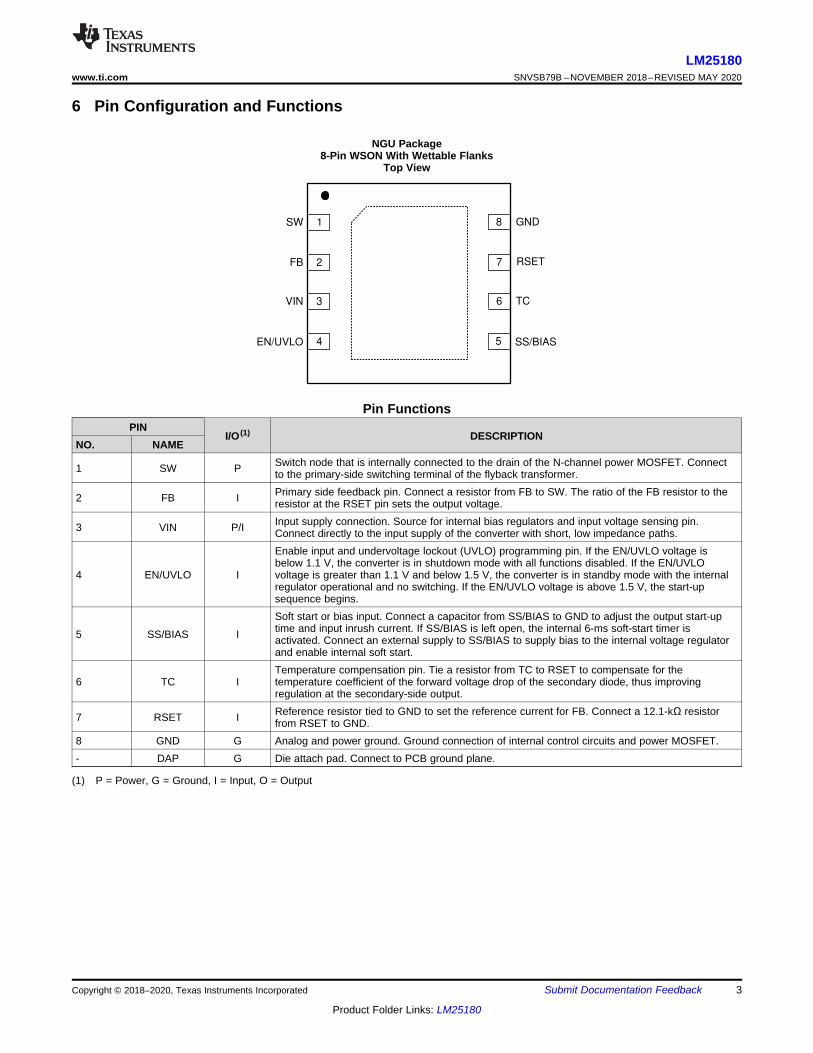
6 Pin Configuration and Functions
NGU Package8-Pin WSON With Wettable Flanks
Top View
Pin FunctionsPIN
I/O (1) DESCRIPTIONNO. NAME
1 SW P Switch node that is internally connected to the drain of the N-channel power MOSFET. Connectto the primary-side switching terminal of the flyback transformer.
2 FB I Primary side feedback pin. Connect a resistor from FB to SW. The ratio of the FB resistor to theresistor at the RSET pin sets the output voltage.
3 VIN P/I Input supply connection. Source for internal bias regulators and input voltage sensing pin.Connect directly to the input supply of the converter with short, low impedance paths.
4 EN/UVLO I
Enable input and undervoltage lockout (UVLO) programming pin. If the EN/UVLO voltage isbelow 1.1 V, the converter is in shutdown mode with all functions disabled. If the EN/UVLOvoltage is greater than 1.1 V and below 1.5 V, the converter is in standby mode with the internalregulator operational and no switching. If the EN/UVLO voltage is above 1.5 V, the start-upsequence begins.
5 SS/BIAS I
Soft start or bias input. Connect a capacitor from SS/BIAS to GND to adjust the output start-uptime and input inrush current. If SS/BIAS is left open, the internal 6-ms soft-start timer isactivated. Connect an external supply to SS/BIAS to supply bias to the internal voltage regulatorand enable internal soft start.
6 TC ITemperature compensation pin. Tie a resistor from TC to RSET to compensate for thetemperature coefficient of the forward voltage drop of the secondary diode, thus improvingregulation at the secondary-side output.
7 RSET I Reference resistor tied to GND to set the reference current for FB. Connect a 12.1-kΩ resistorfrom RSET to GND.
8 GND G Analog and power ground. Ground connection of internal control circuits and power MOSFET.- DAP G Die attach pad. Connect to PCB ground plane.
4
LM25180SNVSB79B –NOVEMBER 2018–REVISED MAY 2020 www.ti.com
Product Folder Links: LM25180
Submit Documentation Feedback Copyright © 2018–2020, Texas Instruments Incorporated
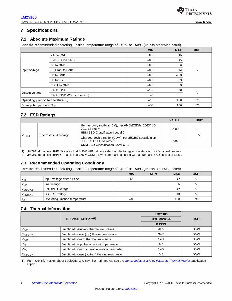
7 Specifications
7.1 Absolute Maximum RatingsOver the recommended operating junction temperature range of –40°C to 150°C (unless otherwise noted)
MIN MAX UNIT
Input voltage
VIN to GND –0.3 45
V
EN/UVLO to GND –0.3 45TC to GND –0.3 6SS/BIAS to GND –0.3 14FB to GND –0.3 45.3FB to VIN –0.3 0.3RSET to GND –0.3 3
Output voltageSW to GND –1.5 70
VSW to GND (20-ns transient) –3
Operating junction temperature, TJ –40 150 °CStorage temperature, Tstg –55 150 °C
(1) JEDEC document JEP155 states that 500-V HBM allows safe manufacturing with a standard ESD control process.(2) JEDEC document JEP157 states that 250-V CDM allows safe manufacturing with a standard ESD control process.
7.2 ESD RatingsVALUE UNIT
V(ESD) Electrostatic discharge
Human body model (HBM), per ANSI/ESDA/JEDEC JS-001, all pins (1)
HBM ESD Classification Level 2±2000
VCharged device model (CDM), per JEDEC specificationJESD22-C101, all pins (2)
CDM ESD Classification Level C4B±500
7.3 Recommended Operating ConditionsOver the recommended operating junction temperature range of –40°C to 150°C (unless otherwise noted)
MIN NOM MAX UNITVIN Input voltage after turn on 4.5 42 VVSW SW voltage 65 VVEN/UVLO EN/UVLO voltage 42 VVSS/BIAS SS/BIAS voltage 13 VTJ Operating junction temperature –40 150 °C
(1) For more information about traditional and new thermal metrics, see the Semiconductor and IC Package Thermal Metrics applicationreport.
7.4 Thermal Information
THERMAL METRIC (1)LM25180
UNITNGU (WSON)8 PINS
RΘJA Junction-to-ambient thermal resistance 41.3 °C/WRΘJC(top) Junction-to-case (top) thermal resistance 34.7 °C/WRΘJB Junction-to-board thermal resistance 19.1 °C/WΨJT Junction-to-top characterization parameter 0.3 °C/WΨJB Junction-to-board characterization parameter 19.2 °C/WRΘJC(bot) Junction-to-case (bottom) thermal resistance 3.2 °C/W

5
LM25180www.ti.com SNVSB79B –NOVEMBER 2018–REVISED MAY 2020
Product Folder Links: LM25180
Submit Documentation FeedbackCopyright © 2018–2020, Texas Instruments Incorporated
7.5 Electrical CharacteristicsTypical values correspond to TJ = 25°C. Minimum and maximum limits aaply over the full –40°C to 150°C junctiontemperature range unless otherwise indicated. VIN = 24 V and VEN/UVLO = 2 V unless otherwise stated.
PARAMETER TEST CONDITIONS MIN TYP MAX UNITSUPPLY CURRENTISHUTDOWN VIN shutdown current VEN/UVLO = 0 V 3 µAIACTIVE VIN active current VEN/UVLO = 2.5 V, VRSET = 1.8 V 260 350 µAIACTIVE-BIAS VIN current with BIAS connected VSS/BIAS = 6 V 25 40 µAVSD-FALLING Shutdown threshold VEN/UVLO falling 0.3 VENABLE AND INPUT UVLOVSD-RISING Standby threshold VEN/UVLO rising 0.8 1 VVUV-RISING Enable threshold VEN/UVLO rising 1.45 1.5 1.53 VVUV-HYST Enable voltage hysteresis VEN/UVLO falling 0.04 0.05 VIUV-HYST Enable current hysteresis VEN/UVLO = 1.6 V 4.2 5 5.5 µAFEEDBACKIRSET RSET current RRSET = 12.1 kΩ 100 µAVRSET RSET regulation voltage RRSET = 12.1 kΩ 1.191 1.21 1.224 VVFB-VIN1 FB to VIN voltage IFB = 80 µA –40 mVVFB-VIN2 FB to VIN voltage IFB = 120 µA 40 mVSWITCHING FREQUENCYFSW-MIN Minimum switching frequency 12 kHzFSW-MAX Maximum switching frequency 350 kHztON-MIN Minimum switch on-time 140 nsDIODE THERMAL COMPENSATIONVTC TC voltage ITC = ±10 µA, TJ = 25°C 1.2 1.27 VPOWER SWITCHESRDS(on) MOSFET on-state resistance ISW = 100 mA 0.4 Ω
SOFT-START AND BIASISS SS ext capacitor charging current 5 µAtSS Internal SS time 6 msVBIAS-UVLO-RISE
BIAS enable voltage VSS/BIAS rising 5.5 5.75 V
VBIAS-UVLO-HYST
BIAS UVLO hysteresis VSS/BIAS falling 190 mV
CURRENT LIMITISW-PEAK Peak current limit threshold 1.23 1.5 1.73 ATHERMAL SHUTDOWNTSD Thermal shutdown threshold TJ rising 175 °CTSD-HYS Thermal shutdown hysteresis 6 °C
Junction Temperature (qC)
Shutd
ow
n Q
uie
scen
t C
urr
en
t (P
A)
-50 -25 0 25 50 75 100 125 1500
3
6
9
12
15
18
D001
VIN = 12 VVIN = 24 VVIN = 42 V
VIN 10V/DIV
2 ms/DIV
VOUT 1V/DIV
IOUT 500mA/DIV
1 Ps/DIV
SW 20V/DIV
1 Ps/DIV
VDFLY 5V/DIV
Output Current (A)
Eff
icie
ncy (
%)
0 0.2 0.4 0.6 0.8 1 1.2 1.460
65
70
75
80
85
90
VIN = 12VVIN = 24VVIN = 36V
Output Current (A)
Ou
tpu
t V
olta
ge
(V
)
0 0.2 0.4 0.6 0.8 1 1.2 1.4 1.64.8
4.85
4.9
4.95
5
5.05
5.1
5.15
5.2
VIN = 12VVIN = 24VVIN = 36V
6
LM25180SNVSB79B –NOVEMBER 2018–REVISED MAY 2020 www.ti.com
Product Folder Links: LM25180
Submit Documentation Feedback Copyright © 2018–2020, Texas Instruments Incorporated
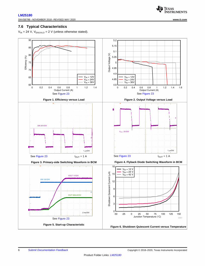
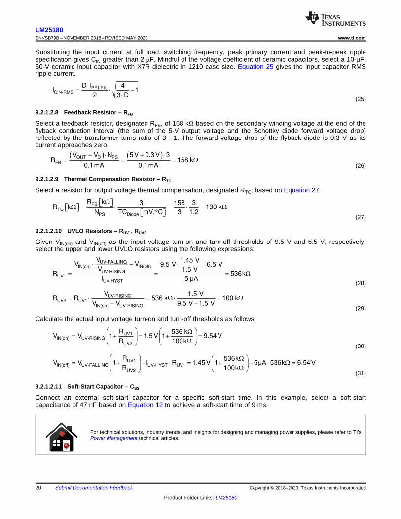
7.6 Typical CharacteristicsVIN = 24 V, VEN/UVLO = 2 V (unless otherwise stated).
See Figure 23
Figure 1. Efficiency versus Load
See Figure 23
Figure 2. Output Voltage versus Load
See Figure 23 IOUT = 1 A
Figure 3. Primary-side Switching Waveform in BCM
See Figure 23 IOUT = 1 A
Figure 4. Flyback Diode Switching Waveform in BCM
See Figure 23
Figure 5. Start-up CharacteristicFigure 6. Shutdown Quiescent Current versus Temperature
Junction Temperature (qC)
TC
Voltage (
V)
-50 -25 0 25 50 75 100 125 1500.8
1
1.2
1.4
1.6
1.8
D006Junction Temperature (qC)
EN
/UV
LO
Th
resh
old
Vo
lta
ge
(V
)
-50 -25 0 25 50 75 100 125 1501.4
1.42
1.44
1.46
1.48
1.5
1.52
1.54
D007
VEN/UVLO RisingVEN/UVLO Falling
Input Voltage (V)
RS
ET
Curr
ent (P
A)
0 6 12 18 24 30 36 4298
99
100
101
102
D004Junction Temperature (qC)
RS
ET
Cu
rrent (P
A)
-50 -25 0 25 50 75 100 125 15096
98
100
102
104
D005
Junction Temperature (qC)
Active
Quie
sce
nt C
urr
en
t (P
A)
-50 -25 0 25 50 75 100 125 150240
250
260
270
280
290
D002
VIN = 12 VVIN = 24 VVIN = 42 V
Junction Temperature (qC)
Active
Quie
sce
nt C
urr
en
t (P
A)
-50 -25 0 25 50 75 100 125 15015
20
25
30
35
D003
VIN = 12 VVIN = 24 VVIN = 42 V
7
LM25180www.ti.com SNVSB79B –NOVEMBER 2018–REVISED MAY 2020
Product Folder Links: LM25180
Submit Documentation FeedbackCopyright © 2018–2020, Texas Instruments Incorporated
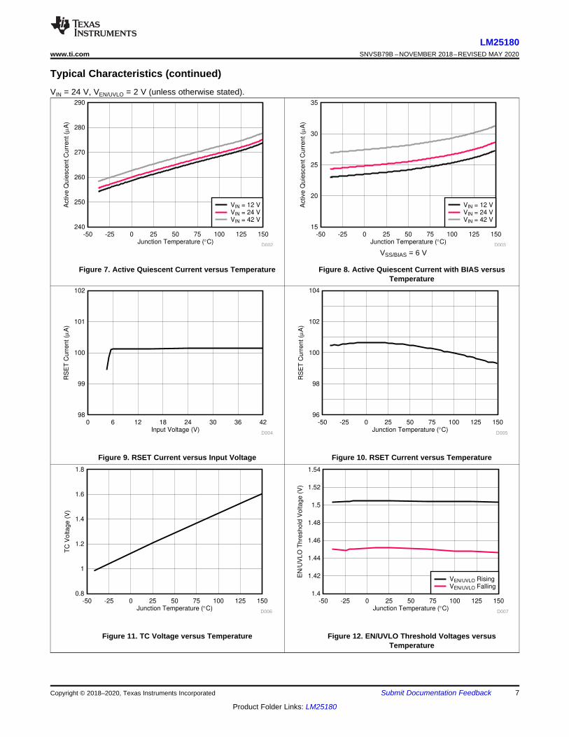
Typical Characteristics (continued)VIN = 24 V, VEN/UVLO = 2 V (unless otherwise stated).
Figure 7. Active Quiescent Current versus Temperature
VSS/BIAS = 6 V
Figure 8. Active Quiescent Current with BIAS versusTemperature
Figure 9. RSET Current versus Input Voltage Figure 10. RSET Current versus Temperature
Figure 11. TC Voltage versus Temperature Figure 12. EN/UVLO Threshold Voltages versusTemperature

Junction Temperature (qC)
Min
. S
witch
ing
Fre
qu
en
cy (
kH
z)
-50 -25 0 25 50 75 100 125 15011
11.5
12
12.5
13
D012Junction Temperature (qC)
Max.
Sw
itchin
g F
reque
ncy (
kH
z)
-50 -25 0 25 50 75 100 125 150320
330
340
350
360
370
380
D013
Junction Temperature (qC)
Peak C
urr
ent Lim
it (
A)
-50 -25 0 25 50 75 100 125 1500
0.3
0.6
0.9
1.2
1.5
1.8
D010
BCMFFM
Junction Temperature (qC)
Min
imum
on-t
ime (
ns)
-50 -25 0 25 50 75 100 125 150130
135
140
145
150
155
160
D011
Junction Temperature (qC)
EN
/UV
LO
Hyste
resis
Cu
rrent
(PA
)
-50 -25 0 25 50 75 100 125 1504.7
4.8
4.9
5
5.1
5.2
5.3
D008Junction Temperature (qC)
Sw
itch R
DS
(on) (:
)
-50 -25 0 25 50 75 100 125 1500.2
0.3
0.4
0.5
0.6
0.7
0.8
D009
8
LM25180SNVSB79B –NOVEMBER 2018–REVISED MAY 2020 www.ti.com
Product Folder Links: LM25180
Submit Documentation Feedback Copyright © 2018–2020, Texas Instruments Incorporated
Typical Characteristics (continued)VIN = 24 V, VEN/UVLO = 2 V (unless otherwise stated).
Figure 13. EN/UVLO Hysteresis Current versus Temperature Figure 14. MOSFET RDS(on) versus Temperature
Figure 15. Switch Peak Current Limits versus Temperature Figure 16. Minimum Switch On-Time versus Temperature
Figure 17. Minimum Switching Frequency versusTemperature
Figure 18. Maximum Switching Frequency versusTemperature
LM25180CIN
CSS
VIN NP : NS
EN/UVLO
VIN
SW
FB
SS/BIASGND
TC
RSET
RFB
VREF
COMP
Internal SS
SAMPLED
FEEDBACK FB 65-V Power MOSFET
Standby
Shutdown
1.1 V
VDD
VDD UVLO
BIAS
REGULATOR
THERMAL
SHUTDOWN
SS/BIAS
VDD
VDD
VIN
1.5 A
ILIM
TRIMMED
REFERENCE
RSET
TC
REGULATION
RTC
VOUT
COUT
DFLY
CONTROL
LOGIC
1.5 V
1.45 V
gm
5 PA
DF
DZ
9
LM25180www.ti.com SNVSB79B –NOVEMBER 2018–REVISED MAY 2020
Product Folder Links: LM25180
Submit Documentation FeedbackCopyright © 2018–2020, Texas Instruments Incorporated
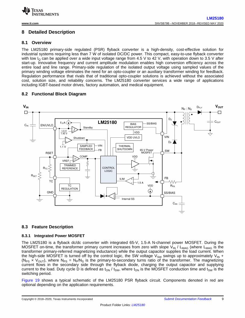
8 Detailed Description
8.1 OverviewThe LM25180 primary-side regulated (PSR) flyback converter is a high-density, cost-effective solution forindustrial systems requiring less than 7 W of isolated DC/DC power. This compact, easy-to-use flyback converterwith low IQ can be applied over a wide input voltage range from 4.5 V to 42 V, with operation down to 3.5 V afterstart-up. Innovative frequency and current amplitude modulation enables high conversion efficiency across theentire load and line range. Primary-side regulation of the isolated output voltage using sampled values of theprimary winding voltage eliminates the need for an opto-coupler or an auxiliary transformer winding for feedback.Regulation performance that rivals that of traditional opto-coupler solutions is achieved without the associatedcost, solution size, and reliability concerns. The LM25180 converter services a wide range of applicationsincluding IGBT-based motor drives, factory automation, and medical equipment.
8.2 Functional Block Diagram
8.3 Feature Description
8.3.1 Integrated Power MOSFETThe LM25180 is a flyback dc/dc converter with integrated 65-V, 1.5-A N-channel power MOSFET. During theMOSFET on-time, the transformer primary current increases from zero with slope VIN / LMAG (where LMAG is thetransformer primary-referred magnetizing inductance) while the output capacitor supplies the load current. Whenthe high-side MOSFET is turned off by the control logic, the SW voltage VSW swings up to approximately VIN +(NPS × VOUT), where NPS = NP/NS is the primary-to-secondary turns ratio of the transformer. The magnetizingcurrent flows in the secondary side through the flyback diode, charging the output capacitor and supplyingcurrent to the load. Duty cycle D is defined as tON / tSW, where tON is the MOSFET conduction time and tSW is theswitching period.
Figure 19 shows a typical schematic of the LM25180 PSR flyback circuit. Components denoted in red areoptional depending on the application requirements.

0
50
100
150
200
250
300
350
400
0 20 40 60 80 100
Sw
itc
hin
g F
rqu
en
cy (
kH
z)
% Total Rated Output Power
Discontinuous conduction mode (DCM) Boundary conduction mode (BCM)
Frequency
foldback mode
(FFM)
VOUT
SW
FB
VIN
EN/UVLO
TC
GND
SS/BIAS
RSET
LM25180
COUT
CIN
T1
VIN
NP : NS
DFLY
RSET
RFB
RTC
CSS
RUV1
RUV2
DCLAMP
DF
DOUT
10
LM25180SNVSB79B –NOVEMBER 2018–REVISED MAY 2020 www.ti.com
Product Folder Links: LM25180
Submit Documentation Feedback Copyright © 2018–2020, Texas Instruments Incorporated
Feature Description (continued)
Figure 19. LM25180 Flyback Converter Schematic (Optional Components in Red)
8.3.2 PSR Flyback Modes of OperationThe LM25180 uses a variable-frequency, peak current-mode (VFPCM) control architecture with three possiblemodes of operation as illustrated in Figure 20.
Figure 20. Three Modes of Operation Illustrated by Variation of Switching Frequency With Load
SET
FB OUT D PS
REF
RR V V N
V
MAG PRI-PK(DCM) SW(DCM)DCM
IN
L I FD
V
OUT OUT DPRI-PK(DCM)
MAG SW(DCM)
2 I V VI
L F
2MAG PRI-PK(DCM)
OUT(DCM) SW(DCM)
L IP F
2
OUT D OUTPRI-PK(BCM)
IN
2 V V II
V D
SW(BCM)
MAG MAGPRI-PK(BCM)
IN PS OUT D
1F
L LI
V N V V
§ · ¨ ¸¨ ¸ © ¹
2MAG PRI-PK(BCM)
OUT(BCM) SW(BCM)
L IP F
2
OUT D PS
IN OUT D PS
V V ND
V V V N
11
LM25180www.ti.com SNVSB79B –NOVEMBER 2018–REVISED MAY 2020
Product Folder Links: LM25180
Submit Documentation FeedbackCopyright © 2018–2020, Texas Instruments Incorporated
Feature Description (continued)The LM25180 operates in boundary conduction mode (BCM) at heavy loads. The power MOSFET turns on whenthe current in the secondary winding reaches zero, and the MOSFET turns off when the peak primary currentreaches the level dictated by the output of the internal error amplifier. As the load is decreased, the frequencyincreases in order to maintain BCM operation. The duty cycle of the flyback converter is given Equation 1, whereVD is the forward voltage drop of the flyback diode as its current approaches zero.
(1)
The output power in BCM is given by Equation 2, where the applicable switching frequency and peak primarycurrent in BCM are specified by Equation 3 and Equation 4, respectively.
(2)
(3)
(4)
As the load decreases, the LM25180 clamps the maximum switching frequency to 350 kHz, and the converterenters discontinuous conduction mode (DCM). The power delivered to the output in DCM is proportional to thepeak primary current squared as given by Equation 5 and Equation 6. Thus, as the load decreases, the peakcurrent reduces to maintain regulation at 350-kHz switching frequency.
(5)
(6)
(7)
At even lighter loads, the primary-side peak current set by the internal error amplifier decreases to a minimumlevel of 0.3 A, or 20% of its 1.5-A peak value, and the MOSFET off-time extends to maintain the output loadrequirement. The system operates in frequency foldback mode (FFM), and the switching frequency decreases asthe load current is reduced. Other than a fault condition, the lowest frequency of operation of the LM25180 is 12kHz, which sets a minimum load requirement of approximately 0.5% full load.
8.3.3 Setting the Output VoltageTo minimize output voltage regulation error, the LM25180 senses the reflected secondary voltage when thesecondary current reaches zero. The feedback (FB) resistor, which is connected between SW and FB as shownin Figure 19, is determined using Equation 8, where RSET is nominally 12.1 kΩ.
(8)
§ · ¨ ¸
© ¹
UV1IN(on) UV-RISING
UV2
RV V 1
R
+
VIN
VCC
5 A
1.5 V
EN/UVLO
UVLO
Comparator
RUV1
RUV2
LM25180
1.45 V
:ª º¬ ¼: ª º¬ ¼ qª º¬ ¼
FB
TC
PS Diode
R k 3R k
N TC mV C
12
LM25180SNVSB79B –NOVEMBER 2018–REVISED MAY 2020 www.ti.com
Product Folder Links: LM25180
Submit Documentation Feedback Copyright © 2018–2020, Texas Instruments Incorporated
Feature Description (continued)8.3.3.1 Diode Thermal CompensationThe LM25180 employs a unique thermal compensation circuit that adjusts the feedback setpoint based on thethermal coefficient of the flyback diode's forward voltage drop. Even though the output voltage is measured whenthe secondary current is effectively zero, there is still a non-zero forward voltage drop associated with the flybackdiode. Select the thermal compensation resistor using Equation 9.
(9)
The temperature coefficient of the diode voltage drop may not be explicitly provided in the diode datasheet, sothe effective value can be estimated based on the measured output voltage shift over temperature when the TCresistor is not installed.
8.3.4 Control Loop Error AmplifierThe inputs of the error amplifier include a level-shifted version of the FB voltage and an internal 1.21-V referenceset by the resistor at RSET. A type-II internal compensation network stabilizes the converter. In BCM operationwhen the output voltage is in regulation, an on-time interval is initiated when the secondary current reaches zero.The power MOSFET is subsequently turned off when an amplified version of the peak primary current exceedsthe error amplifier output.
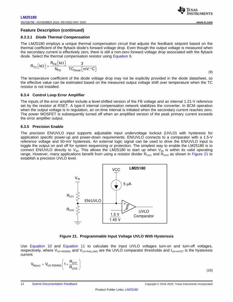
8.3.5 Precision EnableThe precision EN/UVLO input supports adjustable input undervoltage lockout (UVLO) with hysteresis forapplication specific power-up and power-down requirements. EN/UVLO connects to a comparator with a 1.5-Vreference voltage and 50-mV hysteresis. An external logic signal can be used to drive the EN/UVLO input totoggle the output on and off for system sequencing or protection. The simplest way to enable the LM25180 is toconnect EN/UVLO directly to VIN. This allows the LM25180 to start up when VIN is within its valid operatingrange. However, many applications benefit from using a resistor divider RUV1 and RUV2 as shown in Figure 21 toestablish a precision UVLO level.
Figure 21. Programmable Input Voltage UVLO With Hysteresis
Use Equation 10 and Equation 11 to calculate the input UVLO voltages turn-on and turn-off voltages,respectively, where VUV-RISING and VUV-FALLING are the UVLO comparator thresholds and IUV-HYST is the hysteresiscurrent.
(10)

VOUT
SW
FB
VIN
EN/UVLO
TC
GND
RSET
LM25180
COUT
CIN
T1
VIN
NP : NS
DFLY
RSET
RFB
DCLAMP
DF
RUV1
RUV2
DOUT
SS/BIAS
DBIAS1
NP : NAUX
CBIASDBIAS2
22 nF12 V
ª º ª º¬ ¼ ¬ ¼SS SSC nF 5 t ms
§ · ¨ ¸
© ¹
UV1IN(off) UV-FALLING UV-HYST UV1
UV2
RV V 1 I R
R
13
LM25180www.ti.com SNVSB79B –NOVEMBER 2018–REVISED MAY 2020
Product Folder Links: LM25180
Submit Documentation FeedbackCopyright © 2018–2020, Texas Instruments Incorporated
Feature Description (continued)
(11)
The LM25180 also provides a low-IQ shutdown mode when the EN/UVLO voltage is pulled below a base-emittervoltage drop (approximately 0.6 V at room temperature). If the EN/UVLO voltage is below this hard shutdownthreshold, the internal LDO regulator powers off, and the internal bias-supply rail collapses, shutting down thebias currents of the LM25180. The LM25180 operates in standby mode when the EN/UVLO voltage is betweenthe hard shutdown and precision-enable thresholds.
8.3.6 Configurable Soft StartThe LM25180 has a flexible and easy-to-use soft-start control pin, SS/BIAS. The soft-start feature preventsinrush current impacting the LM25180 and the input supply when power is first applied. This is achieved bycontrolling the voltage at the output of the internal error amplifier. Soft start is achieved by slowly ramping up thetarget regulation voltage when the device is first enabled or powered up. Selectable and adjustable start-uptiming options include a 6-ms internally-fixed soft start and an externally-programmable soft start.
The simplest way to use the LM25180 is to leave SS/BIAS open. The LM25180 employs an internal soft-startcontrol ramp and starts up to the regulated output voltage in 6 ms.
However, in applications with a large amount of output capacitance, higher VOUT or other special requirements,the soft-start time can be extended by connecting an external capacitor CSS from SS/BIAS to GND. A longer soft-start time further reduces the supply current needed to charge the output capacitors while sourcing the requiredload current. When the EN/UVLO voltage exceeds the UVLO rising threshold and a delay of 20 µs expires, aninternal current source ISS of 5 µA charges CSS and generates a ramp to control the primary current amplitude.Calculate the soft-start capacitance for a desired soft-start time, tSS, using Equation 12.
(12)
CSS is discharged by an internal FET when switching is disabled by EN/UVLO or thermal shutdown.
8.3.7 External Bias Supply
Figure 22. External Bias Supply Using Transformer Auxiliary Winding
K
§ ·¨ ¸
© ¹
SW-PEAKOUT(max)
OUT
IN PS
II
2 V 1
V N
14
LM25180SNVSB79B –NOVEMBER 2018–REVISED MAY 2020 www.ti.com
Product Folder Links: LM25180
Submit Documentation Feedback Copyright © 2018–2020, Texas Instruments Incorporated
Feature Description (continued)The LM25180 has an external bias supply feature that reduces input quiescent current and increases efficiency.When the voltage at SS/BIAS exceeds a rising threshold of 5.5 V, bias power for the internal LDO regulator canbe derived from an external voltage source or from a transformer auxiliary winding as shown in Figure 22. With abias supply connected, the LM25180 then uses its internal soft-start ramp to control the primary current duringstart-up.
When using a transformer auxiliary winding for bias power, the total leakage current related to diodes DBIAS1 andDBIAS2 in Figure 22 should be less than 1 µA across the full operating temperature range.
8.3.8 Minimum On-Time and Off-TimeWhen the internal power MOSFET is turned off, the leakage inductance of the transformer resonates with theSW node parasitic capacitance. The resultant ringing behavior can be excessive with large transformer leakageinductance and may corrupt the secondary zero-current detection. In order to prevent such a situation, aminimum switch off-time, designated as tOFF-MIN, of maximum 450 ns is set internally to ensure properfunctionality. This sets a lower limit for the transformer magnetizing inductance as discussed in the DetailedDesign Procedure.
Furthermore, noise effects as a result of power MOSFET turn-on can impact the internal current sense circuitmeasurement. To mitigate this effect, the LM25180 provides a blanking time after the MOSFET turns on. Thisblanking time forces a minimum on-time, tON-MIN, of 140 ns.
8.3.9 Overcurrent ProtectionIn case of an overcurrent condition on the isolated output(s), the output voltage drops lower than the regulationlevel since the maximum power delivered is limited by the peak current capability on the primary side. The peakprimary current is maintained at 1.5 A (plus an amount related to the 100-ns propagation delay of the current limitcomparator) until the output decreases to the secondary diode voltage drop to impact the reflected signal on theprimary side. At this point, the LM25180 assumes the output cannot be recovered and re-calibrates its switchingfrequency to 9 kHz until the overload condition is removed. The LM25180 responds with similar behavior to anoutput short circuit condition.
For a given input voltage, Equation 13 gives the maximum output current prior to the engagement of overcurrentprotection. The typical threshold value for ISW-PEAK from the Specifications is 1.5 A.
(13)
A failsafe current limit set at 2.4 A, or 1.6 times the nominal peak current limit, provides redundant fault protectionin case of transformer short circuit or saturation effects. This initiates a 7.5-ms hiccup interval after eightovercurrent events.
8.3.10 Thermal ShutdownThermal shutdown is an integrated self-protection to limit junction temperature and prevent damage related tooverheating. Thermal shutdown turns off the device when the junction temperature exceeds 175°C to preventfurther power dissipation and temperature rise. Junction temperature decreases after shutdown, and the restartswhen the junction temperature falls to 169°C.

15
LM25180www.ti.com SNVSB79B –NOVEMBER 2018–REVISED MAY 2020
Product Folder Links: LM25180
Submit Documentation FeedbackCopyright © 2018–2020, Texas Instruments Incorporated
8.4 Device Functional Modes
8.4.1 Shutdown ModeEN/UVLO facilitates ON and OFF control for the LM25180. When VEN/UVLO is below approximately 0.6 V, thedevice is in shutdown mode. Both the internal LDO and the switching regulator are off. The quiescent current inshutdown mode drops to 3 μA at VIN = 24 V. The LM25180 also employs internal bias rail undervoltageprotection. If the internal bias supply voltage is below its UV threshold, the converter remains off.
8.4.2 Standby ModeThe internal bias rail LDO regulator has a lower enable threshold than the converter itself. When VEN/UVLO isabove 0.6 V and below the precision-enable threshold (1.5 V typically), the internal LDO is on and regulating.The precision enable circuitry is turned on once the internal VCC is above its UV threshold. The switching actionand voltage regulation are not enabled until VEN/UVLO rises above the precision enable threshold.
8.4.3 Active ModeThe LM25180 is in active mode when VEN/UVLO is above the precision-enable threshold and the internal bias railis above its UV threshold. The LM25180 operates in one of three modes depending on the load currentrequirement:1. Boundary conduction mode (BCM) at heavy loads.2. Discontinuous conduction mode (DCM) at medium loads.3. Frequency foldback mode (FFM) at light loads.
Refer to PSR Flyback Modes of Operation for more detail.
IOUT = 1 A
SW
FB
VIN
EN/UVLO
TC
GND
RSET
LM25180
COUT
CIN
100 F
10 F
T1VIN = 10 V...36 V
3 : 1
DFLY
RSET
12.1 k:
RFB
158 k:
DCLAMP
DF
RTC
130 k:
RUV1
536 k:
RUV2
100 k:
DOUT
5.6 V
30 PH
VOUT = 5 V
24 V
SS/BIAS
CSS
47 nF
16
LM25180SNVSB79B –NOVEMBER 2018–REVISED MAY 2020 www.ti.com
Product Folder Links: LM25180
Submit Documentation Feedback Copyright © 2018–2020, Texas Instruments Incorporated
9 Application and Implementation
NOTEInformation in the following applications sections is not part of the TI componentspecification, and TI does not warrant its accuracy or completeness. TI’s customers areresponsible for determining suitability of components for their purposes. Customers shouldvalidate and test their design implementation to confirm system functionality.
9.1 Application InformationThe LM25180 requires only a few external components to convert from a wide range of supply voltages to one ormore isolated output rails. To expedite and streamline the process of designing of a LM25180-based converter, acomprehensive LM25180 quick-start calculator is available for download to assist the designer with componentselection for a given application. WEBENCH® online software is also available to generate complete designs,leveraging iterative design procedures and access to comprehensive component databases. The followingsections discuss the design procedure for both single- and dual-output implementations using specific circuitdesign examples.
As mentioned previously, the LM25180 also integrates several optional features to meet system designrequirements, including precision enable, input UVLO, programmable soft start, output voltage thermalcompensation, and external bias supply connection. Each application incorporates these features as needed fora more comprehensive design.
The application circuits detailed in Typical Applications show LM25180 configuration options suitable for severalapplication use cases. Refer to the LM5180EVM-S05 and LM5180EVM-DUAL EVM user's guides for more detail.
9.2 Typical Applications
For step-by-step design procedures, circuit schematics, bill of materials, PCB files, simulation and test results of LM25180-poweredimplementations, refer to the TI reference designs library.
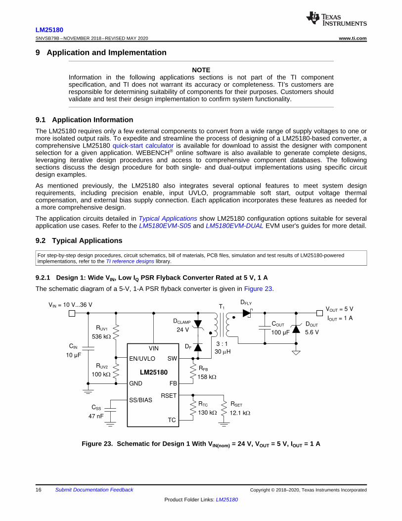
9.2.1 Design 1: Wide VIN, Low IQ PSR Flyback Converter Rated at 5 V, 1 AThe schematic diagram of a 5-V, 1-A PSR flyback converter is given in Figure 23.
Figure 23. Schematic for Design 1 With VIN(nom) = 24 V, VOUT = 5 V, IOUT = 1 A

17
LM25180www.ti.com SNVSB79B –NOVEMBER 2018–REVISED MAY 2020
Product Folder Links: LM25180
Submit Documentation FeedbackCopyright © 2018–2020, Texas Instruments Incorporated
9.2.1.1 Design RequirementsThe required input, output, and performance parameters for this application example are shown in Table 1.
Table 1. Design ParametersDESIGN PARAMETER VALUE
Input voltage range 10 V to 36 VInput UVLO thresholds 9.5 V on, 6.5 V off
Output voltage 5 VRated load current, VIN = 24 V 1 A
Output voltage regulation ±1.5%Output voltage ripple < 100 mV
The target full-load efficiency is 86% based on a nominal input voltage of 24 V and an isolated output voltage of5 V. The LM25180 is chosen to deliver a fixed 5-V output voltage set by resistor RFB connected between the SWand FB pins. The input voltage turn-on and turn-off thresholds are established by RUV1 and RUV2. The requiredcomponents are listed in Table 2. Transformers for other single-output designs are listed in Table 3.
Table 2. List of Components for Design 1REF DES QTY SPECIFICATION VENDOR PART NUMBERCIN 1 10 µF, 50 V, X7R, 1210, ceramic Taiyo Yuden UMK325AB7106KM-T
COUT 1100 µF, 6.3 V, X7S, 1210, ceramic
Murata GRM32EC70J107ME15Taiyo Yuden JMK325AC7107MM-P
100 µF, 6.3 V, X5R, 1210, ceramicTDK C3225X5R0J107M250ACWürth Electronik 885012109004
CSS 1 47 nF, 16 V, X7R, 0402 Std StdDCLAMP 1 Zener, 24 V, 1 W, PowerDI-123 DFLZ24-7 Diodes Inc.DF 1 Switching diode, 75 V, 0.25 A, SOD-323 CMDD4448 Central SemiDFLY 1 Schottky diode, 40 V, 2 A, SOD-123 FSV340FP ONsemiDOUT 1 Zener, 5.6 V, 5%, SOD-523 BZX585-C5V6 NexperiaRFB 1 158 kΩ, 1%, 0402 Std StdRSET 1 12.1 kΩ, 1%, 0402 Std StdRTC 1 130 kΩ, 1%, 0402 Std StdRUV1 1 536 kΩ, 1%, 0603 Std StdRUV2 1 100 kΩ, 1%, 0402 Std Std
T1 130 µH, 2 A, turns ratio 3 : 1, 9.3 × 10.2 mm
Coilcraft YA8779-BLWürth Electronik 750317605
30 µH, 2.6 A, turns ratio 3 : 1, 12.5 × 15.5 mm Sumida 12387-T15140 µH, 2 A, turns ratio 3 : 1, 13.3 × 15.2 mm Würth Electronik 750313974
U1 1 LM25180 PSR flyback converter, VSON-8 Texas Instruments LM25180NGUR
Table 3. Magnetic Components for Other Single-Output DesignsOUTPUT VOLTAGE RANGE TURNS RATIO LMAG, ISAT DIMENSIONS VENDOR PART NUMBER4 V to 8 V 2 : 1
30 µH, 2 A 9.3 × 10.2 × 10.6 mm Coilcraft
YA9033-AL8 V to 11 V 1.5 : 1 YA9034-AL12 V to 18 V 1 : 1 YA9035-AL18 V to 36 V 1 : 2 YA9036-AL36 V to 55 V 1 : 3 YA9037-AL

K ° ®
§ · § · °¨ ¸ ¨ ¸© ¹© ¹
INSW-PEAK
OUT(max)
OUT IN
ININ PS
0.85 A at V 12VI 0.85 1.5 AI
2 2V 5 V 11 1.2A at V 24 V
V 3V N
OUT PRI-PK PS
SEC-RMS
2 I I NI
3
PRI-RMS PRI-PK
DI I
3
t
OUT D PS OFF-MINMAG
SW-PEAK(FFM)
V V N t 5 V + 0.3 V 3 450nsL 24+
I 0.3 A
IN(min)MAXPS
MAX OUT D
VD 0.6 10VN 3
1 D V V 1 0.6 5V + 0.3V
18
LM25180SNVSB79B –NOVEMBER 2018–REVISED MAY 2020 www.ti.com
Product Folder Links: LM25180
Submit Documentation Feedback Copyright © 2018–2020, Texas Instruments Incorporated
9.2.1.2 Detailed Design Procedure
9.2.1.2.1 Custom Design With WEBENCH® Tools
Click here to create a custom design using the LM25180 device with WEBENCH® Power Designer.1. Start by entering the input voltage (VIN), output voltage (VOUT), and output current (IOUT) requirements.2. Optimize the design for key parameters such as efficiency, footprint, and cost using the optimizer dial.3. Compare the generated design with other possible solutions from Texas Instruments.
The WEBENCH Power Designer provides a customized schematic along with a list of materials with real-timepricing and component availability.
In most cases, these actions are available:• Run electrical simulations to see important waveforms and circuit performance• Run thermal simulations to understand board thermal performance• Export customized schematic and layout into popular CAD formats• Print PDF reports for the design, and share the design with colleagues
Get more information about WEBENCH tools at www.ti.com/WEBENCH.
9.2.1.2.2 Custom Design With Excel Quickstart Tool
Select components based on the converter specifications using the LM25180 quick-start calculator.
9.2.1.2.3 Flyback Transformer – T1
Choose a turns ratio based on an approximate 60% max duty cycle at minimum input voltage using Equation 14,rounding up or down as needed.
(14)
Select a magnetizing inductance based on the minimum off-time constraint using Equation 15. Choose a value of30 µH to allow some margin for this application. Specify a saturation current of 2 A, above the maximum switchcurrent specification of the LM25180.
(15)
Note that a higher magnetizing inductance provides a larger operating range for BCM and FFM, but the leakageinductance may increase based on a higher number of primary turns, NP. The primary and secondary windingRMS currents are given by Equation 16 and Equation 17, respectively.
(16)
(17)
Find the maximum output current for a given turns ratio using Equation 18, where the typical value for ISW-PEAK isthe 1.5-A switch current peak threshold. Iterate by increasing the turns ratio if the output current capability is toolow at minimum input voltage.
(18)
2
PRI-PK
IN
SW IN
DI D 1
2C
2 F V
§ · ¨ ¸
© ¹t '
PS PRI-PK
COUT-RMS OUT
OUT
2 N II I 1
3 I
§ · § ·t ¨ ¸ ¨ ¸ ' © ¹ © ¹
22 22
MAG SW-PEAK
OUT
OUT OUT
30+ $L I 1 D 1 0.6C 86)
2 V V 2 2 50mV 5 V 2
DZ(clamp) PS OUT DV 1.5 N V V 1.5 3 5V 0.3V 24V |
DZ(clamp) SW(max) IN(max)V V V
IN(max)D-REV OUT
PS
V 36 VV V 5 V 17 V
N 3t
19
LM25180www.ti.com SNVSB79B –NOVEMBER 2018–REVISED MAY 2020
Product Folder Links: LM25180
Submit Documentation FeedbackCopyright © 2018–2020, Texas Instruments Incorporated
9.2.1.2.4 Flyback Diode – DFLY
The flyback diode reverse voltage is given by Equation 19.
(19)
Select a 40-V, 3-A Schottky diode for this application to account for inevitable diode voltage overshoot andringing related to the resonance of transformer leakage inductance and diode parasitic capacitance. Connect anappropriate RC snubber circuit (for example, 100 Ω and 22 pF) across the flyback diode if needed, particularly ifthe transformer leakage inductance is high. Also, choose a flyback diode with current rating that aligns with themaximum peak secondary winding current of NPS*ISW-PEAK. As mentioned in Layout, place adequate copper atthe cathode of the diode to improve its thermal performance and prevent overheating during high ambienttemperature or overload conditions. Beware of the high leakage current typical of a Schottky diode at elevatedoperating temperatures.
9.2.1.2.5 Zener Clamp Circuit – DF, DCLAMP
Connect a diode-Zener clamping circuit across the primary winding to limit the peak switch-node voltage afterMOSFET turn-off below the maximum level of 65 V, as given by Equation 20.
(20)
Choosing the zener, DCLAMP, with clamp voltage of approximately 1.5 times the reflected output voltage, asspecified by Equation 21, provides a balance between the maximum switch voltage excursion and the leakageinductance demagnetization time.
(21)
Select an ultra-fast switching diode or Schottky diode for DF with rated voltage greater than the maximum inputvoltage and with low forward recovery voltage drop.
9.2.1.2.6 Output Capacitor – COUT
The output capacitor determines the voltage ripple at the converter output, limits the voltage excursion during aload transient, and sets the dominant pole of the converter's small-signal response. For a flyback converterspecifically, the output capacitor supplies the load current when the main switch is on, and therefore the outputvoltage ripple is a function of load current and duty cycle.
Select an output capacitance using Equation 22 to limit the ripple voltage amplitude to less than 1% of the outputvoltage at minimum input voltage and maximum load.
(22)
Select a 100-µF, 6.3-V capacitor in 1210 case size with X5R or better dielectric. Equation 23 gives the outputcapacitor RMS ripple current.
(23)
9.2.1.2.7 Input Capacitor – CIN
Select an input capacitance using Equation 24 to limit the ripple voltage amplitude to less than 5% of the inputvoltage when operating at nominal input voltage.
(24)
§ · § ·: : ¨ ¸ ¨ ¸
:© ¹© ¹
UV1IN(off) UV-FALLING UV-HYST UV1
UV2
R 536kV V 1 I R 1.45V 1 5$ N 9
R 100k
§ · § ·: ¨ ¸ ¨ ¸
:© ¹© ¹
UV1IN(on) UV-RISING
UV2
R 536 kV V 1 1.5 V 1 9.54 V
R 100k
: :
UV-RISINGUV2 UV1
IN(on) UV-RISING
V 1.5 VR R 536 k 100 k
V V 9.5 V 1.5 V
:
UV-FALLINGIN(on) IN(off)
UV-RISINGUV1
UV-HYST
V 1.45 VV V 9.5 V 6.5 V
V 1.5 VR 536k
I 5 $
:ª º¬ ¼: :ª º¬ ¼ qª º¬ ¼
FB
TC
PS Diode
R k 3 158 3R k 130 k
N TC mV C 3 1.2
OUT D PS
FB
V V N 5V 0.3V 3R 158 k
0.1mA 0.1mA
:
PRI-PK
CIN-RMS
D I 4I 1
2 3 D
20
LM25180SNVSB79B –NOVEMBER 2018–REVISED MAY 2020 www.ti.com
Product Folder Links: LM25180
Submit Documentation Feedback Copyright © 2018–2020, Texas Instruments Incorporated
Substituting the input current at full load, switching frequency, peak primary current and peak-to-peak ripplespecification gives CIN greater than 2 μF. Mindful of the voltage coefficient of ceramic capacitors, select a 10-µF,50-V ceramic input capacitor with X7R dielectric in 1210 case size. Equation 25 gives the input capacitor RMSripple current.
(25)
9.2.1.2.8 Feedback Resistor – RFB
Select a feedback resistor, designated RFB, of 158 kΩ based on the secondary winding voltage at the end of theflyback conduction interval (the sum of the 5-V output voltage and the Schottky diode forward voltage drop)reflected by the transformer turns ratio of 3 : 1. The forward voltage drop of the flyback diode is 0.3 V as itscurrent approaches zero.
(26)
9.2.1.2.9 Thermal Compensation Resistor – RTC
Select a resistor for output voltage thermal compensation, designated RTC, based on Equation 27.
(27)
9.2.1.2.10 UVLO Resistors – RUV1, RUV2
Given VIN(on) and VIN(off) as the input voltage turn-on and turn-off thresholds of 9.5 V and 6.5 V, respectively,select the upper and lower UVLO resistors using the following expressions:
(28)
(29)
Calculate the actual input voltage turn-on and turn-off thresholds as follows:
(30)
(31)
9.2.1.2.11 Soft-Start Capacitor – CSS
Connect an external soft-start capacitor for a specific soft-start time. In this example, select a soft-startcapacitance of 47 nF based on Equation 12 to achieve a soft-start time of 9 ms.
For technical solutions, industry trends, and insights for designing and managing power supplies, please refer to TI'sPower Management technical articles.
VIN 10V/DIV
2 ms/DIV
VOUT 1V/DIV
IOUT 500mA/DIV
EN 1V/DIV
2 ms/DIV
VOUT 1V/DIV
IOUT 500mA/DIV
Output Current (A)
Ou
tpu
t V
olta
ge
(V
)
0 0.2 0.4 0.6 0.8 1 1.2 1.4 1.64.8
4.85
4.9
4.95
5
5.05
5.1
5.15
5.2
VIN = 12VVIN = 24VVIN = 36V
Output Current (A)
Outp
ut
Voltage (
V)
0.001 0.01 0.1 1 24.8
4.9
5
5.1
5.2
VIN = 12VVIN = 24VVIN = 36V
Output Current (A)
Eff
icie
ncy (
%)
0 0.2 0.4 0.6 0.8 1 1.2 1.460
65
70
75
80
85
90
VIN = 12VVIN = 24VVIN = 36V
Output Current (A)
Eff
icie
ncy (
%)
0.001 0.01 0.1 1 230
40
50
60
70
80
90
100
VIN = 12VVIN = 24VVIN = 36V
21
LM25180www.ti.com SNVSB79B –NOVEMBER 2018–REVISED MAY 2020
Product Folder Links: LM25180
Submit Documentation FeedbackCopyright © 2018–2020, Texas Instruments Incorporated
9.2.1.3 Application CurvesUnless otherwise stated, application performance curves were taken at TA = 25°C.
Figure 24. Efficiency (Linear Scale) Figure 25. Efficiency (Log Scale)
Figure 26. Load Regulation (Linear Scale) Figure 27. Load Regulation (Log Scale)
VIN stepped to 24 V 5-Ω Load
Figure 28. Start-up Characteristic
VIN = 24 V 5-Ω Load
Figure 29. Enable ON Characteristic

Start 150 kHz Stop 30 MHz
Average detector
Peak detector
Start 30 MHz Stop 108 MHz
Average detector Peak detector
1 Ps/DIV
SW 20V/DIV
1 Ps/DIV
VDFLY 5V/DIV
22
LM25180SNVSB79B –NOVEMBER 2018–REVISED MAY 2020 www.ti.com
Product Folder Links: LM25180
Submit Documentation Feedback Copyright © 2018–2020, Texas Instruments Incorporated
VIN = 24 V IOUT = 1 A
Figure 30. Switch Voltage
VIN = 24 V IOUT = 1 A
Figure 31. Flyback Diode Voltage
VIN = 24 VIOUT = 0.85 A 150 kHz to 30 MHz LIN = 4.7 µH
CIN = 10 µF
Figure 32. CISPR 25 Class 5 Conducted EMI Plot
VIN = 24 VIOUT = 0.85 A 30 MHz to 108 MHz LIN = 4.7 µH
CIN = 10 µF
Figure 33. CISPR 25 Class 5 Conducted EMI Plot
IOUT1 = 0.2 A
CIN
22 F
10 F
T1VIN = 9.5 V...36 V
1 : 1 : 0.52
RSET
12.1 k:
RFB
154 k:
DCLAMP
DF
RTC
200 k:
RUV1
RUV2
68.1 k:
DOUT1
18 V
30 PH
VOUT1 = 15 V
47 F
DOUT2
8.2 V
SW
FB
VIN
EN/UVLO
TC
GND
SS/BIAS
RSET
LM25180
DFLY1
COUT1
COUT2
DFLY2
IOUT2 = ±0.2 A
VOUT2 = ±7.7 V
340 k:24 V
23
LM25180www.ti.com SNVSB79B –NOVEMBER 2018–REVISED MAY 2020
Product Folder Links: LM25180
Submit Documentation FeedbackCopyright © 2018–2020, Texas Instruments Incorporated
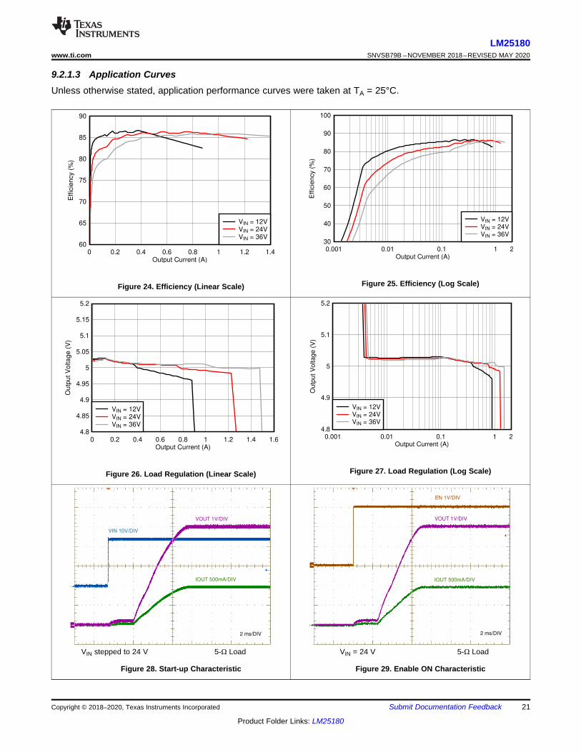
9.2.2 Design 2: PSR Flyback Converter With Dual Outputs of 15 V and –7.7 V at 200 mAThe schematic diagram of a dual-output flyback converter intended for isolated IGBT and SiC MOSFET gatedrive power supply applications is given in Figure 34.
Figure 34. Schematic for Design 2 With VIN(nom) = 24 V, VOUT1 = 15 V, VOUT2 = –7.7 V, IOUT = 200 mA
9.2.2.1 Design RequirementsThe required input, output, and performance parameters for this application example are shown in Table 4.
Table 4. Design ParametersDESIGN PARAMETER VALUE
Input voltage range (steady state) 9.5 V to 36 VOutput 1 voltage and current 15 V, 0.2 AOutput 2 voltage and current –7.7 V, –0.2 A
Input UVLO thresholds 9 V on, 7 V offOutput voltage regulation ±2%
The target full-load efficiency of this LM25180 design is 88% based on a nominal input voltage of 24 V andisolated output voltages of 15 V and –7.7 V sharing a common return. The selected flyback convertercomponents are cited in Table 5, including multi-winding flyback transformer, input and output capacitors,rectifying diodes and flyback converter IC.

t
OUT D PS OFF-MINMAG
SW-PEAK(FFM)
V V N t 15V + 0.35V 1 450nsL 23+
I 0.3A
|
IN(min)MAXPS
MAX OUT D
VD 0.6 9.5VN 1
1 D V V 1 0.6 15V + 0.4V
S2 OUT2 D2
S1 OUT1 D1
N V V 7.7 V 0.4 V0.52
N V V 15 V 0.6 V
24
LM25180SNVSB79B –NOVEMBER 2018–REVISED MAY 2020 www.ti.com
Product Folder Links: LM25180
Submit Documentation Feedback Copyright © 2018–2020, Texas Instruments Incorporated
Table 5. List of Components for Design 2REF DES QTY SPECIFICATION VENDOR PART NUMBERCIN 1 10 µF, 50 V, X7R, 1210, ceramic Taiyo Yuden UMK325AB7106KM-T
COUT1 1 22 µF, 25 V, X7R, 1210, ceramicTDK C3225X7R1E226MMurata GRM32ER71E226KE15LTaiyo Yuden TMK325B7226MM-TR
COUT2 1 47 µF, 10 V, X7R, 1210, ceramicTDK C3225X7R1A476MMurata GRM32ER71A476ME15LTaiyo Yuden LMK325B7476MM-TR
DFLY1 1 Schottky diode, 100 V, 1 A, PowerDI-123 DFLS1100-7 Diodes Inc.DFLY2 1 Schottky diode, 60 V, 1 A, PowerDI-123 DFLS160-7 Diodes Inc.DCLAMP 1 Zener, 24 V, 1 W, PowerDI-123 DFLZ24-7 Diodes Inc.DF 1 Switching diode, 75 V, 0.3 A, SOD323 1N4148WS Diodes Inc.DOUT1 1 Zener, 18 V, 5%, SOD523 BZX585-C18 NexperiaDOUT2 1 Zener, 8.2 V, 2%, SOD523 BZX585-B8V2 NexperiaRFB 1 154 kΩ, 1%, 0402 Std StdRSET 1 12.1 kΩ, 1%, 0402 Std StdRTC 1 200 kΩ, 1%, 0402 Std StdRUV1 1 340 kΩ, 1%, 0603 Std StdRUV2 1 68.1 kΩ, 1%, 0402 Std Std
T1 1 30 µH, 2 A, turns ratio 1 : 1: 0.52, 9 × 10 mm, SMTCoilcraft YA8916-BLDWürth Electronik 750317595
U1 1 LM25180 PSR flyback converter, VSON-8 Texas Instruments LM25180NGUR
9.2.2.2 Detailed Design ProcedureUsing the LM25180 quick-start calculator, components are selected based on the flyback converterspecifications.
9.2.2.2.1 Flyback Transformer – T1
Set the turns ratio of the transformer secondary windings using Equation 32, where NS1 and NS2 are the numberof secondary turns for the respective outputs.
(32)
Choose a primary-secondary turns ratio of 1 : 1 for the 15-V output based on an approximate 60% duty cycle atminimum input voltage using Equation 33. The transformer turns ratio for both outputs is thus specified as 1 : 1 :0.52.
(33)
Select a magnetizing inductance based on the minimum off-time constraint using Equation 34. Choose a value of30 µH and a saturation current of 2 A for this application.
(34)
Find the maximum output current for a given turns ratio, assuming the outputs are symmetrically loaded, usingEquation 35.

: :
UV-RISINGUV2 UV1
IN(on) UV-RISING
V 1.5 VR R 340 k 68 k
V V 9 V 1.5 V
:
UV-FALLINGIN(on) IN(off)
UV-RISINGUV1
UV-HYST
V 1.45 VV V 9 V 7 V
V 1.5 VR 340k
I 5 $
OUT D PS
FB
V V N 15 V 0.3 V 1R 154 k
0.1mA 0.1mA
:
IN(max)D2-REV OUT2
PS
VV V 36V 0.52 7.7V 26.4V
Nt
IN(max)D1-REV OUT1
PS
V 36VV V 15V 51V
N 1t
K ° ®§ · § · ° ¨ ¸ ¨ ¸¨ ¸© ¹ © ¹
INSW-PEAK
OUT(max)
OUT IN
IN PS IN
0.2A at V 12VI 0.9 1.5 AI
2 2V 1 0.27A at V 24V22.7V 1
V N V 11.52
25
LM25180www.ti.com SNVSB79B –NOVEMBER 2018–REVISED MAY 2020
Product Folder Links: LM25180
Submit Documentation FeedbackCopyright © 2018–2020, Texas Instruments Incorporated
(35)
9.2.2.2.2 Flyback Diodes – DFLY1 and DFLY2
The flyback diode reverse voltages for the positive and negative outputs are given respectively by Equation 36and Equation 25.
(36)
(37)
Choose 100-V, 1-A and 60-V, 1-A Schottky diodes for the positive and negative outputs, respectively, to allowsome margin for inevitable voltage overshoot and ringing related to leakage inductance and diode capacitance. Ifneeded, use a diode RC snubber circuit, for example 100 Ω and 22 pF, to mitigate such overshoot and ringing.
9.2.2.2.3 Input Capacitor – CIN
The input capacitor, CIN, filters the primary-side triangular current waveform. To prevent large ripple voltage, usea low-ESR ceramic input capacitor sized according to Equation 24 for the RMS ripple current given byEquation 25. In this design example, choose a 10-µF, 50-V ceramic input capacitor with X7R dielectric and 1210footprint.
9.2.2.2.4 Feedback Resistor – RFB
Install a 154-kΩ resistor from SW to FB based on an output voltage setpoint of 15 V (plus a flyback diode voltagedrop) reflected to the primary by a transformer turns ratio of unity.
(38)
9.2.2.2.5 UVLO Resistors – RUV1, RUV2
Given VIN(on) and VIN(off) as the input voltage turn-on and turn-off thresholds of 9 V and 7 V, respectively, selectthe upper and lower UVLO resistors using Equation 39 and Equation 40.
(39)
(40)

VOUT1 5V/DIV
VIN 10V/DIV
2 ms/DIV
VOUT2 5V/DIV
IOUT1 50mA/DIV
VOUT1 5V/DIV
EN 1V/DIV
2 ms/DIV
VOUT2 5V/DIV
IOUT1 100mA/DIV
Output Current (mA)
Outp
ut
Voltage (
V)
0 50 100 150 200 250 300 350 40022
22.2
22.4
22.6
22.8
23
23.2
23.4VIN = 12VVIN = 24VVIN = 36V
Output Current (mA)
Ou
tpu
t V
olta
ge
(V
)
1 10 100 40040022
22.4
22.8
23.2
23.6
24VIN = 12VVIN = 24VVIN = 36V
Output Current (mA)
Eff
icie
ncy (
%)
0 50 100 150 200 250 30050
55
60
65
70
75
80
85
90
95
100
VIN = 12VVIN = 24VVIN = 36V
Output Current (mA)
Eff
icie
ncy (
%)
1 10 100 30030030
40
50
60
70
80
90
100
VIN = 12VVIN = 24VVIN = 36V
26
LM25180SNVSB79B –NOVEMBER 2018–REVISED MAY 2020 www.ti.com
Product Folder Links: LM25180
Submit Documentation Feedback Copyright © 2018–2020, Texas Instruments Incorporated
9.2.2.3 Application Curves
Figure 35. Efficiency (Linear Scale) Figure 36. Efficiency (Log Scale)
Total of VOUT1 and VOUT2
Figure 37. Load Regulation (Linear Scale)
Total of VOUT1 and VOUT2
Figure 38. Load Regulation (Log Scale)
VIN stepped to 24 V 75 Ω and 40 Ω Loads
Figure 39. Start-Up Characteristic
VIN = 24 V 75 Ω and 40 Ω Loads
Figure 40. ENABLE ON Characteristic

VOUT1 1V/DIV
IOUT2 100mA/DIV
200 Ps/DIV
IOUT1 100mA/DIV
VOUT2 0.5V/DIV
VOUT1 1V/DIV
IOUT2 100mA/DIV
200 Ps/DIV
IOUT1 100mA/DIV
VOUT2 0.5V/DIV
1 Ps/DIV
SW 20V/DIV
VDFLY2 20V/DIV
1 Ps/DIV
VDFLY1 20V/DIV
27
LM25180www.ti.com SNVSB79B –NOVEMBER 2018–REVISED MAY 2020
Product Folder Links: LM25180
Submit Documentation FeedbackCopyright © 2018–2020, Texas Instruments Incorporated
VIN = 24 V
Figure 41. Switch Voltage, Full Load
VIN = 24 V
Figure 42. Flyback Diode Voltages, Full Load
VIN = 24 V IOUT1 = 200 mA
Figure 43. Output 1 Load Transient, 50 mA to 200 mA
VIN = 24 V IOUT2 = 200 mA
Figure 44. Output 2 Load Transient, 50 mA to 200 mA
IOUT1 = 0.1 A
CIN
10 F
10 F
T1VIN = 8.5 V...42 V
1 : 1.5 : 0.4
RSET
12.1 k:
RFB
130 k:
DCLAMP
DF
RTC
301 k:
RUV1
RUV2
34 k:
DOUT1
27 V
30 PH
VOUT1 = 24 V
47 F
COUT1
COUT2
147 k:22 V
SW
FB
VIN
EN/UVLO
TC
GND
SS/BIAS
RSET
LM25180
DFLY1
DFLY2
DOUT2
5.6 V
IOUT2 = 0.3 A
VOUT2 = 5 V
28
LM25180SNVSB79B –NOVEMBER 2018–REVISED MAY 2020 www.ti.com
Product Folder Links: LM25180
Submit Documentation Feedback Copyright © 2018–2020, Texas Instruments Incorporated
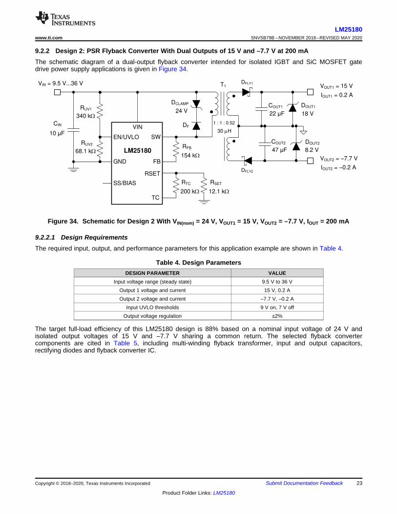
9.2.3 Design 3: PSR Flyback Converter With Stacked Dual Outputs of 24 V and 5 VThe schematic diagram of a dual-output flyback converter with high-voltage secondary stacked on the low-voltage secondary winding is given in Figure 45. This configuration reduces the number of turns for the high-voltage output, resulting in lower secondary-to-secondary leakage inductance for improved output voltage crossregulation.
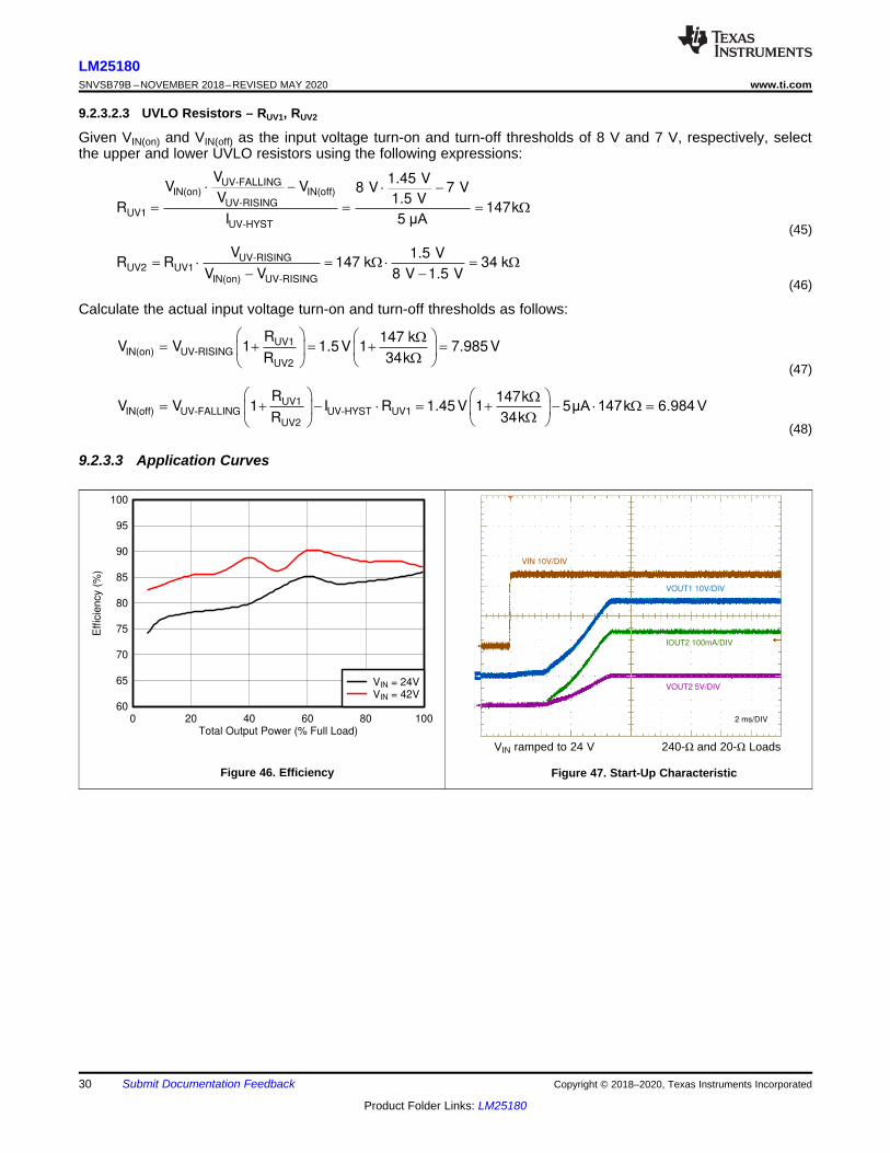
Figure 45. Schematic for Design 3 With VIN(nom) = 24 V, VOUT1 = 24 V, VOUT2 = 5 V
9.2.3.1 Design RequirementsThe required input, output, and performance parameters for this application example are shown in Table 6.
Table 6. Design ParametersDESIGN PARAMETER VALUE
Input voltage range (steady state) 8.5 V to 42 VOutput 1 voltage and current 24 V, 0.1 AOutput 2 voltage and current 5 V, 0.3 A
Input UVLO thresholds 8 V on, 7 V offOutput voltage regulation ±2%
The target full-load efficiency of this LM25180 design is 88% based on a nominal input voltage of 24 V andisolated output voltages of 24 V and 5 V. The selected flyback converter components are cited in Table 7,including multi-winding flyback transformer, input and output capacitors, rectifying diodes, and converter IC.

OUT D PS
FB
V V N 5 V 0.25 V 2.5R 130 k
0.1mA 0.1mA
:
t
OUT1 D1 PS1 OFF-MINMAG
SW-PEAK(FFM)
V V N t 19 V + 0.6 V 11.5 450nsL 19.4+
I 0.3 A
S2 OUT2 D2
S1 OUT1 D1
N V V 5 V 0.3 V0.27
N V V 19 V 0.6 V
IN(min)P MAXPS1
S1 MAX OUT D
VN D 0.6 8.5 VN 0.65
N 1 D V V 1 0.6 19 V + 0.6 V
29
LM25180www.ti.com SNVSB79B –NOVEMBER 2018–REVISED MAY 2020
Product Folder Links: LM25180
Submit Documentation FeedbackCopyright © 2018–2020, Texas Instruments Incorporated
Table 7. List of Components for Design 3REF DES QTY SPECIFICATION VENDOR PART NUMBER
CIN, COUT1 210 µF, 50 V, X7R, 1210, ceramic Taiyo Yuden UMK325AB7106MM-T10 µF, 50 V, X7S, 1210, ceramic TDK C3225X7R1H106M
COUT2 1 47 µF, 10 V, X7R, 1210, ceramic Murata GRM32ER71A476ME15LDFLY1 1 Switching diode, fast recovery, 200 V, 1 A, SOD-123 DFLU1200 Diodes Inc.DFLY2 1 Schottky diode, 40 V, 1 A, SOD-123 B140HW Diodes Inc.DCLAMP 1 Zener, 22 V, 1 W, PowerDI-123 DFLZ22-7 Diodes Inc.DF 1 Switching diode, 75 V, 0.25 A, SOD-323 CMDD4448 Central SemiDOUT1 1 Zener, 27 V, 2%, SOD-523 BZX585-B27 NexperiaDOUT2 1 Zener, 5.6 V, 2%, SOD-523 BZX585-B5V6 NexperiaRFB 1 130 kΩ, 1%, 0402 Std StdRSET 1 12.1 kΩ, 1%, 0402 Std StdRTC 1 301 kΩ, 1%, 0402 Std StdRUV1 1 147 kΩ, 1%, 0603 Std StdRUV2 1 34 kΩ, 1%, 0402 Std Std
T1 130 µH, 2 A, turns ratio 1 : 1.5 : 0.4, 9 × 10 mm, SMT Coilcraft YA8864-BLD
30 µH, 2 A, turns ratio 1 : 1 : 0.55, 9 × 10 mm, SMTCoilcraft YA8916-BLDWürth Electronik 750317595
U1 1 LM25180 PSR flyback converter, VSON-8 Texas Instruments LM25180NGUR
9.2.3.2 Detailed Design ProcedureComponents are selected based on the converter specifications using the LM25180 quick-start calculator. Thedesign procedure is similar to that outlined for Designs 1 and 2 previously.
9.2.3.2.1 Flyback Transformer – T1
The 24-V output is DC stacked on top of the 5-V output as they share a common return connection. This enableslower secondary-to-secondary leakage inductance for better cross regulation and also reduced rectifier diodereverse voltage stress. Choose a primary-secondary turns ratio for the effective 19-V secondary based on anapproximate 60% max duty cycle at minimum input voltage using Equation 41.
(41)
Set the turns ratio of the transformer secondary windings using Equation 42. The transformer turns ratio for bothoutputs is thus specified as 1 : 1.5 : 0.4.
(42)
Select a magnetizing inductance based on the minimum off-time constraint using Equation 43. Choose a value of30 µH and a saturation current of minimum 2 A for this application.
(43)
9.2.3.2.2 Feedback Resistor – RFB
Install a 130-kΩ resistor from SW to FB based on the secondary winding voltage (the sum of the 5-V outputvoltage and the Schottky diode forward voltage drop) reflected by the relevant transformer turns ratio, which inthis design is 1 : 0.4 or 2.5 : 1.
(44)
VOUT1 10V/DIV
2 ms/DIV
VOUT2 5V/DIV
IOUT2 100mA/DIV
VIN 10V/DIV
Total Output Power (% Full Load)
Eff
icie
ncy (
%)
0 20 40 60 80 10060
65
70
75
80
85
90
95
100
VIN = 24VVIN = 42V
§ · § ·: : ¨ ¸ ¨ ¸
:© ¹© ¹
UV1IN(off) UV-FALLING UV-HYST UV1
UV2
R 147kV V 1 I R 1.45 V 1 5$ N 9
R 34k
§ · § ·: ¨ ¸ ¨ ¸
:© ¹© ¹
UV1IN(on) UV-RISING
UV2
R 147 kV V 1 1.5 V 1 7.985 V
R 34k
: :
UV-RISINGUV2 UV1
IN(on) UV-RISING
V 1.5 VR R 147 k 34 k
V V 8 V 1.5 V
:
UV-FALLINGIN(on) IN(off)
UV-RISINGUV1
UV-HYST
V 1.45 VV V 8 V 7 V
V 1.5 VR 147k
I 5 $
30
LM25180SNVSB79B –NOVEMBER 2018–REVISED MAY 2020 www.ti.com
Product Folder Links: LM25180
Submit Documentation Feedback Copyright © 2018–2020, Texas Instruments Incorporated
9.2.3.2.3 UVLO Resistors – RUV1, RUV2
Given VIN(on) and VIN(off) as the input voltage turn-on and turn-off thresholds of 8 V and 7 V, respectively, selectthe upper and lower UVLO resistors using the following expressions:
(45)
(46)
Calculate the actual input voltage turn-on and turn-off thresholds as follows:
(47)
(48)
9.2.3.3 Application Curves
Figure 46. Efficiency
VIN ramped to 24 V 240-Ω and 20-Ω Loads
Figure 47. Start-Up Characteristic
VOUT1 200mV/DIV
400 Ps/DIVVOUT2 100mV/DIV
IOUT2 100mA/DIV
IOUT1 20mA/DIV
VOUT1 200mV/DIV
400 Ps/DIVVOUT2 100mV/DIV
IOUT2 50mA/DIV
IOUT1 50mA/DIV
1 Ps/DIV
SW 20V/DIV
VDFLY1 50V/DIV
1 Ps/DIV
VDFLY2 10V/DIV
VOUT1 10V/DIV
2 ms/DIV
VOUT2 5V/DIV
IOUT2 100mA/DIV
EN 2V/DIV VOUT1 10V/DIV
400 Ps/DIV
VOUT2 5V/DIV
IOUT2 100mA/DIV
IOUT1 100mA/DIV
31
LM25180www.ti.com SNVSB79B –NOVEMBER 2018–REVISED MAY 2020
Product Folder Links: LM25180
Submit Documentation FeedbackCopyright © 2018–2020, Texas Instruments Incorporated
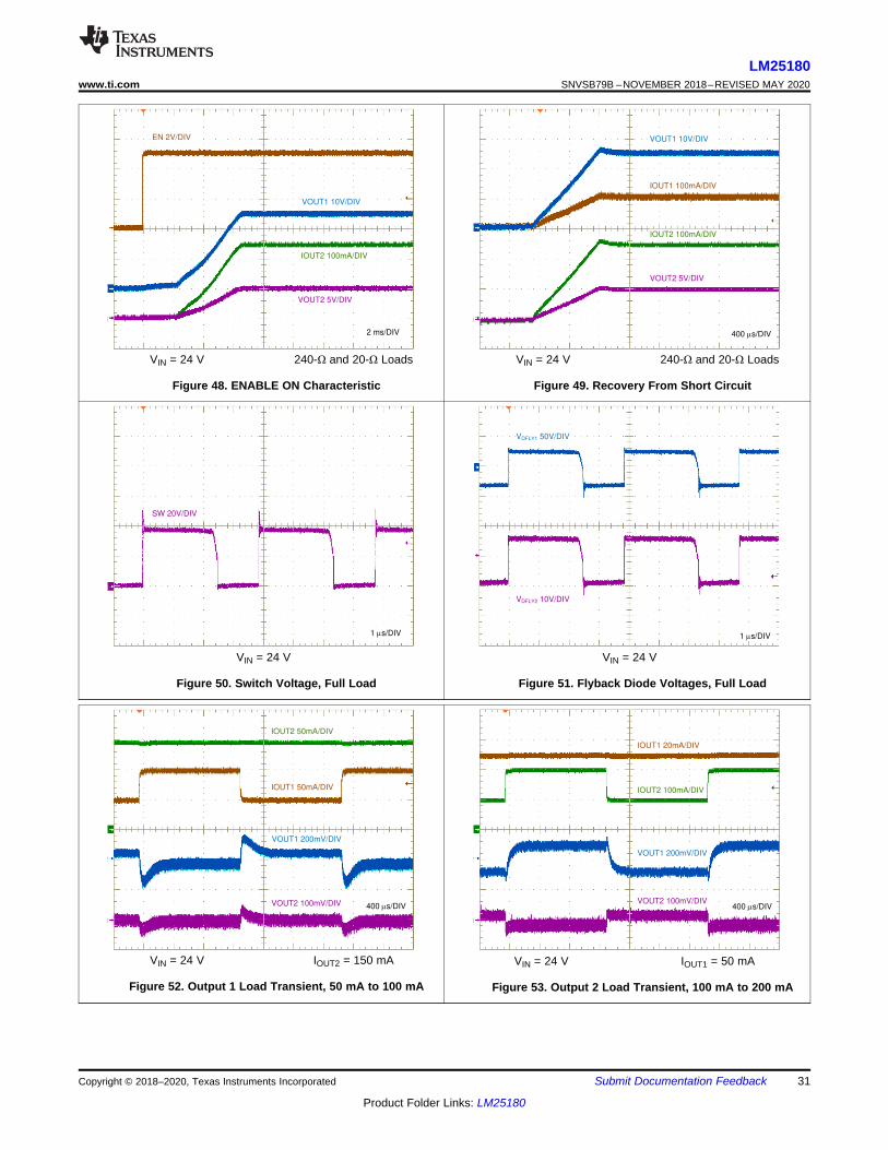
VIN = 24 V 240-Ω and 20-Ω Loads
Figure 48. ENABLE ON Characteristic
VIN = 24 V 240-Ω and 20-Ω Loads
Figure 49. Recovery From Short Circuit
VIN = 24 V
Figure 50. Switch Voltage, Full Load
VIN = 24 V
Figure 51. Flyback Diode Voltages, Full Load
VIN = 24 V IOUT2 = 150 mA
Figure 52. Output 1 Load Transient, 50 mA to 100 mA
VIN = 24 V IOUT1 = 50 mA
Figure 53. Output 2 Load Transient, 100 mA to 200 mA

K
IN
OUTOUTIN
V
IVI
32
LM25180SNVSB79B –NOVEMBER 2018–REVISED MAY 2020 www.ti.com
Product Folder Links: LM25180
Submit Documentation Feedback Copyright © 2018–2020, Texas Instruments Incorporated
10 Power Supply RecommendationsThe LM25180 PSR flyback converter operates over a wide input voltage range from 4.5 V to 42 V. Thecharacteristics of the input supply must be compatible with the Specifications. In addition, the input supply mustbe capable of delivering the required input current to the fully-loaded regulator. Estimate the average inputcurrent with Equation 49.
where• η is the efficiency (49)
If the converter is connected to an input supply through long wires or PCB traces with a large impedance, specialcare is required to achieve stable performance. The parasitic inductance and resistance of the input cables mayhave an adverse affect on converter operation. The parasitic inductance in combination with the low-ESRceramic input capacitors form an underdamped resonant circuit. This circuit can cause overvoltage transients atVIN each time the input supply is cycled ON and OFF. The parasitic resistance causes the input voltage to dipduring a load transient. If the regulator is operating close to the minimum input voltage, this dip can cause falseUVLO fault triggering and a system reset. The best way to solve such issues is to reduce the distance from theinput supply to the regulator and use an aluminum electrolytic input capacitor in parallel with the ceramics. Themoderate ESR of the electrolytic capacitors helps to damp the input resonant circuit and reduce any voltageovershoots. A capacitance in the range of 10 µF to 47 µF is usually sufficient to provide input damping and helpsto hold the input voltage steady during large load transients. A typical ESR of 0.25 Ω provides enough dampingfor most input circuit configurations.
An EMI input filter is often used in front of the regulator that, unless carefully designed, can lead to instability aswell as some of the effects mentioned above. The application report Simple Success with Conducted EMI forDC-DC Converters provides helpful suggestions when designing an input filter for any switching regulator.

33
LM25180www.ti.com SNVSB79B –NOVEMBER 2018–REVISED MAY 2020
Product Folder Links: LM25180
Submit Documentation FeedbackCopyright © 2018–2020, Texas Instruments Incorporated
11 LayoutThe performance of any switching converter depends as much upon PCB layout as it does the componentselection. The following guidelines are provided to assist with designing a PCB with the best power conversionperformance, thermal performance, and minimized generation of unwanted EMI. Figure 54 and Figure 55 providelayout examples for single-output and dual-output designs, respectively.
11.1 Layout GuidelinesPCB layout is a critical for good power supply design. There are several paths that conduct high slew-ratecurrents or voltages that can interact with transformer leakage inductance or parasitic capacitance to generatenoise and EMI or degrade the performance of the power supply.1. Bypass the VIN pin to GND with a low-ESR ceramic capacitor, preferably of X7R or X7S dielectric. Place CIN
as close as possible to the LM25180 VIN and GND pins. Ground return paths for the input capacitor orcapacitors must consist of localized top-side planes that connect to the GND pin and exposed PAD.
2. Minimize the loop area formed by the input capacitor connections and the VIN and GND pins.3. Locate the transformer close to the SW pin. Minimize the area of the SW trace or plane to prevent excessive
e-field or capacitive coupling.4. Minimize the loop area formed by the diode-Zener clamp circuit connections and the primary winding
terminals of the transformer.5. Minimize the loop area formed by the flyback rectifying diode, output capacitor and the secondary winding
terminals of the transformer.6. Connect adequate copper at the cathode of the flyback diode to prevent overheating during overload or high
ambient temperature conditions.7. Tie the GND pin directly to the power pad under the device and to a heat-sinking PCB ground plane.8. Use a ground plane in one of the middle layers as a noise shielding and heat dissipation path.9. Have a single-point ground connection to the plane. Route the return connections for the reference resistor,
soft-start, and enable components directly to the GND pin. This prevents any switched or load currents fromflowing in analog ground traces. If not properly handled, poor grounding results in degraded load regulationor erratic output voltage ripple behavior.
10. Make VIN+, VOUT+ and ground bus connections short and wide. This reduces any voltage drops on the inputor output paths of the converter and maximizes efficiency.
11. Minimize trace length to the FB pin. Locate the feedback resistor close to the FB pin.12. Locate components RSET, RTC and CSS as close as possible to their respective pins. Route with minimal
trace lengths.13. Place a capacitor between input and output return connections to route common-mode noise currents
directly back to their source.14. Provide adequate heatsinking for the LM25180 to keep the junction temperature below 150°C. For
operation at full rated load, the top-side ground plane is an important heat-dissipating area. Use an array ofheat-sinking vias to connect the exposed PAD to the PCB ground plane. If the PCB has multiple copperlayers, connect these thermal vias to inner-layer ground planes. The connection to VOUT+ providesheatsinking for the flyback diode.

Locate the converter IC close
to the transformer and connect
to the GND plane as shown
Minimize the area of the
secondary winding,
flyback diode and output
capacitor switching loops
Place the ceramic input
capacitor close to the IC to
minimize the switching loop area
Place the RSET, TC, FB and SS small-signal
components near their respective pins
Maintain the appropriate primary-
to-secondary clearance distance
Locate the converter IC close
to the transformer and connect
to the GND plane as shown
Place the Y-cap close to the transformer so that common-mode
currents from the secondary to the primary side return in a tight loop
Keep the DZ clamp and RC snubber
components close to the primary winding pins
Keep the secondary
winding, flyback diode
and output capacitor
loop as tight as possible
Place the input capacitor close
to the VIN pin and connect to
the GND plane under the IC
Locate the RSET, TC and FB resistors and
the SS capacitor close to their respective pins
Use adequate heatsinking
copper connected to the
cathode of the flyback
diode (VOUT)
34
LM25180SNVSB79B –NOVEMBER 2018–REVISED MAY 2020 www.ti.com
Product Folder Links: LM25180
Submit Documentation Feedback Copyright © 2018–2020, Texas Instruments Incorporated
11.2 Layout Examples
Figure 54. Single-Output PCB Layout
Figure 55. Dual-Output PCB Layout
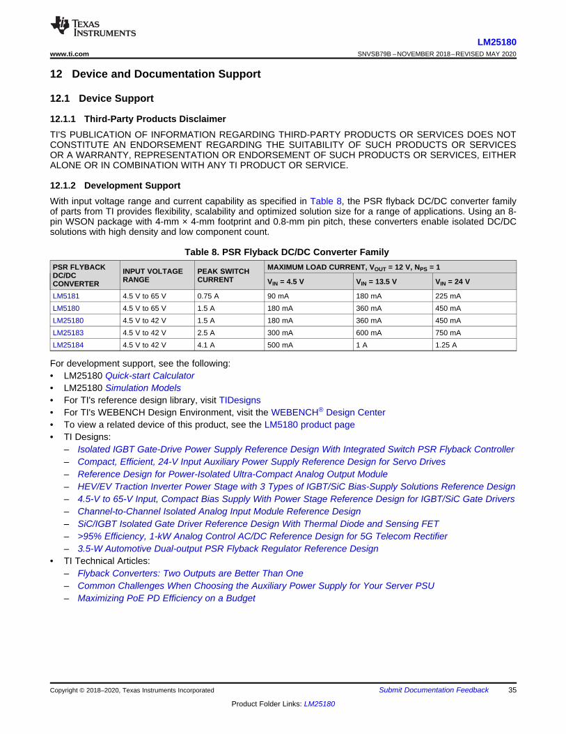
35
LM25180www.ti.com SNVSB79B –NOVEMBER 2018–REVISED MAY 2020
Product Folder Links: LM25180
Submit Documentation FeedbackCopyright © 2018–2020, Texas Instruments Incorporated
12 Device and Documentation Support
12.1 Device Support
12.1.1 Third-Party Products DisclaimerTI'S PUBLICATION OF INFORMATION REGARDING THIRD-PARTY PRODUCTS OR SERVICES DOES NOTCONSTITUTE AN ENDORSEMENT REGARDING THE SUITABILITY OF SUCH PRODUCTS OR SERVICESOR A WARRANTY, REPRESENTATION OR ENDORSEMENT OF SUCH PRODUCTS OR SERVICES, EITHERALONE OR IN COMBINATION WITH ANY TI PRODUCT OR SERVICE.
12.1.2 Development SupportWith input voltage range and current capability as specified in Table 8, the PSR flyback DC/DC converter familyof parts from TI provides flexibility, scalability and optimized solution size for a range of applications. Using an 8-pin WSON package with 4-mm × 4-mm footprint and 0.8-mm pin pitch, these converters enable isolated DC/DCsolutions with high density and low component count.
Table 8. PSR Flyback DC/DC Converter FamilyPSR FLYBACKDC/DCCONVERTER
INPUT VOLTAGERANGE
PEAK SWITCHCURRENT
MAXIMUM LOAD CURRENT, VOUT = 12 V, NPS = 1
VIN = 4.5 V VIN = 13.5 V VIN = 24 V
LM5181 4.5 V to 65 V 0.75 A 90 mA 180 mA 225 mALM5180 4.5 V to 65 V 1.5 A 180 mA 360 mA 450 mALM25180 4.5 V to 42 V 1.5 A 180 mA 360 mA 450 mALM25183 4.5 V to 42 V 2.5 A 300 mA 600 mA 750 mALM25184 4.5 V to 42 V 4.1 A 500 mA 1 A 1.25 A
For development support, see the following:• LM25180 Quick-start Calculator• LM25180 Simulation Models• For TI's reference design library, visit TIDesigns• For TI's WEBENCH Design Environment, visit the WEBENCH® Design Center• To view a related device of this product, see the LM5180 product page• TI Designs:
– Isolated IGBT Gate-Drive Power Supply Reference Design With Integrated Switch PSR Flyback Controller– Compact, Efficient, 24-V Input Auxiliary Power Supply Reference Design for Servo Drives– Reference Design for Power-Isolated Ultra-Compact Analog Output Module– HEV/EV Traction Inverter Power Stage with 3 Types of IGBT/SiC Bias-Supply Solutions Reference Design– 4.5-V to 65-V Input, Compact Bias Supply With Power Stage Reference Design for IGBT/SiC Gate Drivers– Channel-to-Channel Isolated Analog Input Module Reference Design– SiC/IGBT Isolated Gate Driver Reference Design With Thermal Diode and Sensing FET– >95% Efficiency, 1-kW Analog Control AC/DC Reference Design for 5G Telecom Rectifier– 3.5-W Automotive Dual-output PSR Flyback Regulator Reference Design
• TI Technical Articles:– Flyback Converters: Two Outputs are Better Than One– Common Challenges When Choosing the Auxiliary Power Supply for Your Server PSU– Maximizing PoE PD Efficiency on a Budget

36
LM25180SNVSB79B –NOVEMBER 2018–REVISED MAY 2020 www.ti.com
Product Folder Links: LM25180
Submit Documentation Feedback Copyright © 2018–2020, Texas Instruments Incorporated
12.1.3 Custom Design With WEBENCH® ToolsClick here to create a custom design using the LM25180 device with WEBENCH® Power Designer.1. Start by entering the input voltage (VIN), output voltage (VOUT), and output current (IOUT) requirements.2. Optimize the design for key parameters such as efficiency, footprint, and cost using the optimizer dial.3. Compare the generated design with other possible solutions from Texas Instruments.
The WEBENCH Power Designer provides a customized schematic along with a list of materials with real-timepricing and component availability.
In most cases, these actions are available:• Run electrical simulations to see important waveforms and circuit performance• Run thermal simulations to understand board thermal performance• Export customized schematic and layout into popular CAD formats• Print PDF reports for the design, and share the design with colleagues
Get more information about WEBENCH tools at www.ti.com/WEBENCH.
12.2 Documentation Support
12.2.1 Related DocumentationFor related documentation see the following:• LM5180EVM-S05 EVM User's Guide (SNVU592)• LM5180EVM-DUAL EVM User's Guide (SNVU609)• LM25184EVM-S12 EVM User's Guide (SNVU680)• How an Auxless PSR-Flyback Converter can Increase PLC Reliability and Density (SLYT779)• Why Use PSR-Flyback Isolated Converters in Dual-Battery mHEV Systems (SLYT791)• IC Package Features Lead to Higher Reliability in Demanding Automotive and Communications Equipment
Systems (SNVA804)• PSR Flyback DC/DC Converter Transformer Design for mHEV Applications (SNVA805)• Flyback Transformer Design Considerations for Efficiency and EMI (SLUP338)• Under the Hood of Flyback SMPS Designs (SLUP261)• White Papers:
– Valuing Wide VIN, Low EMI Synchronous Buck Circuits for Cost-driven, Demanding Applications(SLYY104)
– An Overview of Conducted EMI Specifications for Power Supplies (SLYY136)– An Overview of Radiated EMI Specifications for Power Supplies (SLYY142)
• AN-2162: Simple Success with Conducted EMI from DC-DC Converters (SNVA489)• Using New Thermal Metrics (SBVA025)• Semiconductor and IC Package Thermal Metrics (SPRA953)
12.3 Receiving Notification of Documentation UpdatesTo receive notification of documentation updates, go to the device product folder on ti.com. In the upper rightcorner, click on Alert me to register for a weekly digest of any product information that has changed. For changedetails, review the revision history included in any revised document.
12.4 Support ResourcesTI E2E™ support forums are an engineer's go-to source for fast, verified answers and design help — straightfrom the experts. Search existing answers or ask your own question to get the quick design help you need.
Linked content is provided "AS IS" by the respective contributors. They do not constitute TI specifications and donot necessarily reflect TI's views; see TI's Terms of Use.
12.5 TrademarksE2E is a trademark of Texas Instruments.

37
LM25180www.ti.com SNVSB79B –NOVEMBER 2018–REVISED MAY 2020
Product Folder Links: LM25180
Submit Documentation FeedbackCopyright © 2018–2020, Texas Instruments Incorporated
12.5 Trademarks (continued)WEBENCH is a registered trademark of Texas Instruments.All other trademarks are the property of their respective owners.
12.6 Electrostatic Discharge CautionThis integrated circuit can be damaged by ESD. Texas Instruments recommends that all integrated circuits be handled withappropriate precautions. Failure to observe proper handling and installation procedures can cause damage.
ESD damage can range from subtle performance degradation to complete device failure. Precision integrated circuits may be moresusceptible to damage because very small parametric changes could cause the device not to meet its published specifications.
12.7 GlossarySLYZ022 — TI Glossary.
This glossary lists and explains terms, acronyms, and definitions.
13 Mechanical, Packaging, and Orderable InformationThe following pages have mechanical, packaging, and orderable information. This information is the most currentdata available for the designated devices. This data is subject to change without notice and revision of thisdocument. For browser-based versions of this data sheet, refer to the left-hand navigation.
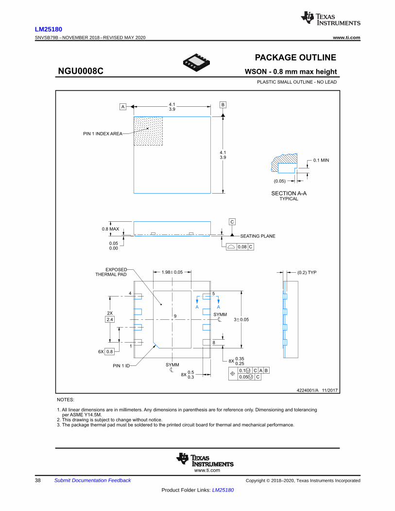
A A
www.ti.com
PACKAGE OUTLINE
C
8X0.350.25
3 0.05
2X
2.4
1.98 0.05
6X 0.8
0.8 MAX
8X0.50.3
0.050.00
A4.13.9
B
4.13.9
(0.2) TYP
0.1 MIN
(0.05)
WSON - 0.8 mm max heightNGU0008CPLASTIC SMALL OUTLINE - NO LEAD
4224001/A 11/2017
PIN 1 INDEX AREA
SEATING PLANE
0.08 C
1
4 5
8
PIN 1 ID0.1 C A B
0.05 C
THERMAL PADEXPOSED
SYMM
SYMM9
NOTES:
1. All linear dimensions are in millimeters. Any dimensions in parenthesis are for reference only. Dimensioning and tolerancingper ASME Y14.5M.
2. This drawing is subject to change without notice.3. The package thermal pad must be soldered to the printed circuit board for thermal and mechanical performance.
SCALE 3.000
A-A 30.000
SECTION A-ATYPICAL
38
LM25180SNVSB79B –NOVEMBER 2018–REVISED MAY 2020 www.ti.com
Product Folder Links: LM25180
Submit Documentation Feedback Copyright © 2018–2020, Texas Instruments Incorporated
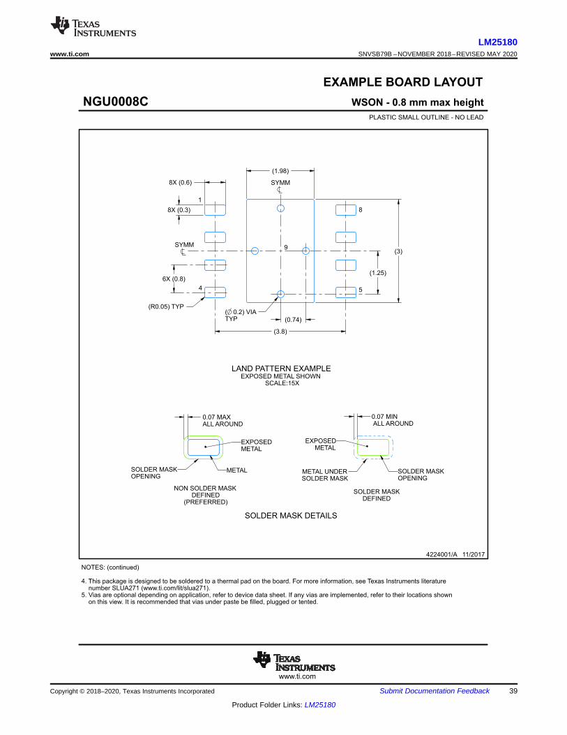
www.ti.com
EXAMPLE BOARD LAYOUT
0.07 MINALL AROUND
0.07 MAXALL AROUND
8X (0.3)
(3)
(3.8)
6X (0.8)
(1.98)
( 0.2) VIATYP (0.74)
(1.25)
8X (0.6)
(R0.05) TYP
WSON - 0.8 mm max heightNGU0008CPLASTIC SMALL OUTLINE - NO LEAD
4224001/A 11/2017
SYMM
1
4 5
8
EXPOSED METAL SHOWNLAND PATTERN EXAMPLE
SCALE:15X
SYMM 9
NOTES: (continued)
4. This package is designed to be soldered to a thermal pad on the board. For more information, see Texas Instruments literaturenumber SLUA271 (www.ti.com/lit/slua271).
5. Vias are optional depending on application, refer to device data sheet. If any vias are implemented, refer to their locations shownon this view. It is recommended that vias under paste be filled, plugged or tented.
SOLDER MASKOPENINGSOLDER MASK
METAL UNDER
SOLDER MASKDEFINED
EXPOSEDMETAL
METALSOLDER MASKOPENING
NON SOLDER MASK
SOLDER MASK DETAILS
DEFINED(PREFERRED)
EXPOSEDMETAL
39
LM25180www.ti.com SNVSB79B –NOVEMBER 2018–REVISED MAY 2020
Product Folder Links: LM25180
Submit Documentation FeedbackCopyright © 2018–2020, Texas Instruments Incorporated

www.ti.com
EXAMPLE STENCIL DESIGN
(R0.05) TYP
8X (0.3)
8X (0.6)
(1.75)
(1.31)
(3.8)
(0.755)
6X (0.8)
WSON - 0.8 mm max heightNGU0008CPLASTIC SMALL OUTLINE - NO LEAD
4224001/A 11/2017
NOTES: (continued)
6. Laser cutting apertures with trapezoidal walls and rounded corners may offer better paste release. IPC-7525 may have alternatedesign recommendations.
SOLDER PASTE EXAMPLEBASED ON 0.125 mm THICK STENCIL
EXPOSED PAD 9:77% PRINTED SOLDER COVERAGE BY AREA UNDER PACKAGE
SCALE:20X
SYMM
1
45
8
METALTYP
SYMM9
40
LM25180SNVSB79B –NOVEMBER 2018–REVISED MAY 2020 www.ti.com
Product Folder Links: LM25180
Submit Documentation Feedback Copyright © 2018–2020, Texas Instruments Incorporated
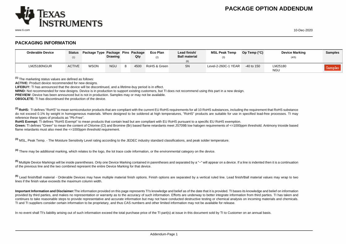
PACKAGE OPTION ADDENDUM
www.ti.com 10-Dec-2020
Addendum-Page 1
PACKAGING INFORMATION
Orderable Device Status(1)
Package Type PackageDrawing
Pins PackageQty
Eco Plan(2)
Lead finish/Ball material
(6)
MSL Peak Temp(3)
Op Temp (°C) Device Marking(4/5)
Samples
LM25180NGUR ACTIVE WSON NGU 8 4500 RoHS & Green SN Level-2-260C-1 YEAR -40 to 150 LM25180NGU
(1) The marketing status values are defined as follows:ACTIVE: Product device recommended for new designs.LIFEBUY: TI has announced that the device will be discontinued, and a lifetime-buy period is in effect.NRND: Not recommended for new designs. Device is in production to support existing customers, but TI does not recommend using this part in a new design.PREVIEW: Device has been announced but is not in production. Samples may or may not be available.OBSOLETE: TI has discontinued the production of the device.
(2) RoHS: TI defines "RoHS" to mean semiconductor products that are compliant with the current EU RoHS requirements for all 10 RoHS substances, including the requirement that RoHS substancedo not exceed 0.1% by weight in homogeneous materials. Where designed to be soldered at high temperatures, "RoHS" products are suitable for use in specified lead-free processes. TI mayreference these types of products as "Pb-Free".RoHS Exempt: TI defines "RoHS Exempt" to mean products that contain lead but are compliant with EU RoHS pursuant to a specific EU RoHS exemption.Green: TI defines "Green" to mean the content of Chlorine (Cl) and Bromine (Br) based flame retardants meet JS709B low halogen requirements of <=1000ppm threshold. Antimony trioxide basedflame retardants must also meet the <=1000ppm threshold requirement.
(3) MSL, Peak Temp. - The Moisture Sensitivity Level rating according to the JEDEC industry standard classifications, and peak solder temperature.
(4) There may be additional marking, which relates to the logo, the lot trace code information, or the environmental category on the device.
(5) Multiple Device Markings will be inside parentheses. Only one Device Marking contained in parentheses and separated by a "~" will appear on a device. If a line is indented then it is a continuationof the previous line and the two combined represent the entire Device Marking for that device.
(6) Lead finish/Ball material - Orderable Devices may have multiple material finish options. Finish options are separated by a vertical ruled line. Lead finish/Ball material values may wrap to twolines if the finish value exceeds the maximum column width.
Important Information and Disclaimer:The information provided on this page represents TI's knowledge and belief as of the date that it is provided. TI bases its knowledge and belief on informationprovided by third parties, and makes no representation or warranty as to the accuracy of such information. Efforts are underway to better integrate information from third parties. TI has taken andcontinues to take reasonable steps to provide representative and accurate information but may not have conducted destructive testing or chemical analysis on incoming materials and chemicals.TI and TI suppliers consider certain information to be proprietary, and thus CAS numbers and other limited information may not be available for release.
In no event shall TI's liability arising out of such information exceed the total purchase price of the TI part(s) at issue in this document sold by TI to Customer on an annual basis.

PACKAGE OPTION ADDENDUM
www.ti.com 10-Dec-2020
Addendum-Page 2
OTHER QUALIFIED VERSIONS OF LM25180 :
• Automotive: LM25180-Q1
NOTE: Qualified Version Definitions:
• Automotive - Q100 devices qualified for high-reliability automotive applications targeting zero defects
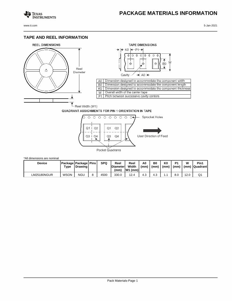
TAPE AND REEL INFORMATION
*All dimensions are nominal
Device PackageType
PackageDrawing
Pins SPQ ReelDiameter
(mm)
ReelWidth
W1 (mm)
A0(mm)
B0(mm)
K0(mm)
P1(mm)
W(mm)
Pin1Quadrant
LM25180NGUR WSON NGU 8 4500 330.0 12.4 4.3 4.3 1.1 8.0 12.0 Q1
PACKAGE MATERIALS INFORMATION
www.ti.com 5-Jan-2021
Pack Materials-Page 1
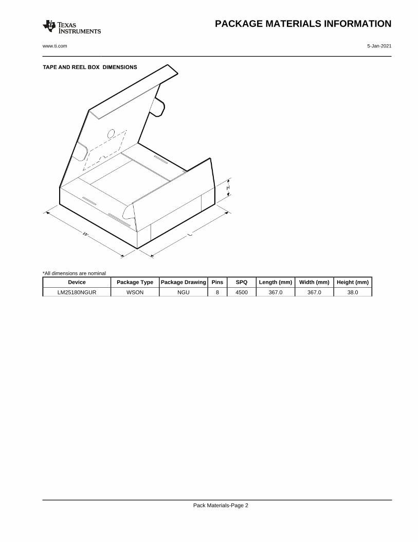
*All dimensions are nominal
Device Package Type Package Drawing Pins SPQ Length (mm) Width (mm) Height (mm)
LM25180NGUR WSON NGU 8 4500 367.0 367.0 38.0
PACKAGE MATERIALS INFORMATION
www.ti.com 5-Jan-2021
Pack Materials-Page 2
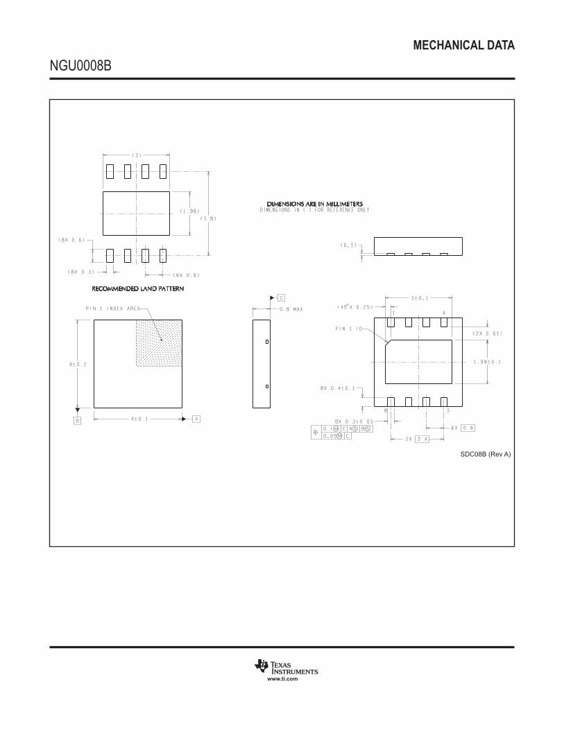
MECHANICAL DATA
NGU0008B
www.ti.com
SDC08B (Rev A)

IMPORTANT NOTICE AND DISCLAIMERTI PROVIDES TECHNICAL AND RELIABILITY DATA (INCLUDING DATASHEETS), DESIGN RESOURCES (INCLUDING REFERENCEDESIGNS), APPLICATION OR OTHER DESIGN ADVICE, WEB TOOLS, SAFETY INFORMATION, AND OTHER RESOURCES “AS IS”AND WITH ALL FAULTS, AND DISCLAIMS ALL WARRANTIES, EXPRESS AND IMPLIED, INCLUDING WITHOUT LIMITATION ANYIMPLIED WARRANTIES OF MERCHANTABILITY, FITNESS FOR A PARTICULAR PURPOSE OR NON-INFRINGEMENT OF THIRDPARTY INTELLECTUAL PROPERTY RIGHTS.These resources are intended for skilled developers designing with TI products. You are solely responsible for (1) selecting the appropriateTI products for your application, (2) designing, validating and testing your application, and (3) ensuring your application meets applicablestandards, and any other safety, security, or other requirements. These resources are subject to change without notice. TI grants youpermission to use these resources only for development of an application that uses the TI products described in the resource. Otherreproduction and display of these resources is prohibited. No license is granted to any other TI intellectual property right or to any third partyintellectual property right. TI disclaims responsibility for, and you will fully indemnify TI and its representatives against, any claims, damages,costs, losses, and liabilities arising out of your use of these resources.TI’s products are provided subject to TI’s Terms of Sale (https:www.ti.com/legal/termsofsale.html) or other applicable terms available eitheron ti.com or provided in conjunction with such TI products. TI’s provision of these resources does not expand or otherwise alter TI’sapplicable warranties or warranty disclaimers for TI products.IMPORTANT NOTICE
Mailing Address: Texas Instruments, Post Office Box 655303, Dallas, Texas 75265Copyright © 2021, Texas Instruments Incorporated