Cinelabs Flyback Installation Guide for Atari's Amplifone ...
Upload
khangminh22Category
view
3download
0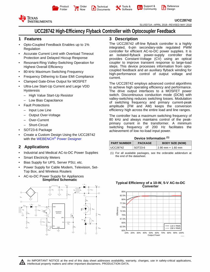
Output Power
Effi
cien
cy
10% 20% 30% 40% 50% 60% 70% 80% 90% 100%60%
62.5%
65%
67.5%
70%
72.5%
75%
77.5%
80%
82.5%
85%
D001
115 V RMS230 V RMS
UCC28742SOT23-6
DRV
CS
VDD
GND
VS
NP NS
NA
VAUX
VAC
FB
+
±
ZFB
IFB
+ VFA -
IOPT
VVDD
RFB4
RFB3
VE
CFB3
CVDD
RTL
RFB2
RFB1
ROPT
COUT
RCS
RLC
RS2
RS1
RSTR
CB2CB1
+ VF -VOUT
VBULK
Product
Folder
Order
Now
Technical
Documents
Tools &
Software
Support &Community
ReferenceDesign
An IMPORTANT NOTICE at the end of this data sheet addresses availability, warranty, changes, use in safety-critical applications,intellectual property matters and other important disclaimers. PRODUCTION DATA.
UCC28742SLUSD71A –APRIL 2018–REVISED MAY 2018
UCC28742 High-Efficiency Flyback Controller with Optocoupler Feedback
1
1 Features1• Opto-Coupled Feedback Enables up to 1%
Regulation• Accurate Current Limit with Overload Timeout
Protection and Delayed Hiccup Response• Resonant-Ring Valley-Switching Operation for
Highest Overall Efficiency• 80-kHz Maximum Switching Frequency• Frequency Dithering to Ease EMI Compliance• Clamped Gate-Drive Output for MOSFET• Ultra-Low Start-Up Current and Large VDD
Hysteresis– High Value Start-Up Resistor– Low Bias Capacitance
• Fault Protections– Input Low Line– Output Over-Voltage– Over-Current– Short-Circuit
• SOT23-6 Package• Create a Custom Design Using the UCC28742
with the WEBENCH® Power Designer
2 Applications• Industrial and Medical AC-to-DC Power Supplies• Smart Electricity Meters• Bias Supply for UPS, Server PSU, etc.• Power Supply for Cable Modem, Television, Set-
Top Box, and Wireless Routers• AC-to-DC Power Supply for Appliances
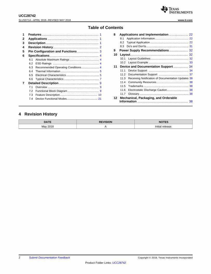
3 DescriptionThe UCC28742 off-line flyback controller is a highlyintegrated, 6-pin secondary-side regulated PWMcontroller for efficient AC-to-DC power supplies. It isan isolated-flyback power-supply controller thatprovides Constant-Voltage (CV) using an opticalcoupler to improve transient response to large-loadsteps. This device processes information from opto-coupled feedback and an auxiliary flyback winding forhigh-performance control of output voltage andcurrent.
The UCC28742 employs advanced control algorithmsto achieve high operating efficiency and performance.The drive output interfaces to a MOSFET powerswitch. Discontinuous conduction mode (DCM) withvalley-switching reduces switching losses. Modulationof switching frequency and primary current-peakamplitude (FM and AM) keeps the conversionefficiency high across the entire load and line ranges.
The controller has a maximum switching frequency of80 kHz and always maintains control of the peak-primary current in the transformer. A minimumswitching frequency of 200 Hz facilitates theachievement of low no-load input power.
Device Information (1)
PART NUMBER PACKAGE BODY SIZE (NOM)UCC28742 SOT23-6 2.90 mm × 1.60 mm
(1) For all available packages, see the orderable addendum atthe end of the datasheet.
Simplified SchematicTypical Efficiency of a 10-W, 5-V AC-to-DC
Converter
2
UCC28742SLUSD71A –APRIL 2018–REVISED MAY 2018 www.ti.com
Product Folder Links: UCC28742
Submit Documentation Feedback Copyright © 2018, Texas Instruments Incorporated
Table of Contents1 Features .................................................................. 12 Applications ........................................................... 13 Description ............................................................. 14 Revision History..................................................... 25 Pin Configuration and Functions ......................... 36 Specifications......................................................... 4
6.1 Absolute Maximum Ratings ...................................... 46.2 ESD Ratings ............................................................ 46.3 Recommended Operating Conditions....................... 46.4 Thermal Information .................................................. 56.5 Electrical Characteristics........................................... 56.6 Typical Characteristics .............................................. 7
7 Detailed Description .............................................. 97.1 Overview ................................................................... 97.2 Functional Block Diagram ......................................... 97.3 Feature Description................................................. 107.4 Device Functional Modes........................................ 21
8 Applications and Implementation ...................... 228.1 Application Information............................................ 228.2 Typical Application .................................................. 228.3 Do's and Don'ts....................................................... 31
9 Power Supply Recommendations ...................... 3210 Layout................................................................... 32
10.1 Layout Guidelines ................................................. 3210.2 Layout Example .................................................... 33
11 Device and Documentation Support ................. 3411.1 Device Support .................................................... 3411.2 Documentation Support ....................................... 3711.3 Receiving Notification of Documentation Updates 3811.4 Community Resources.......................................... 3811.5 Trademarks ........................................................... 3811.6 Electrostatic Discharge Caution............................ 3811.7 Glossary ................................................................ 38
12 Mechanical, Packaging, and OrderableInformation ........................................................... 38
4 Revision History
DATE REVISION NOTESMay 2018 A Initial release.
1
2
3
6
5
4
VDD
DRV
VS
GND
CS
FB
3
UCC28742www.ti.com SLUSD71A –APRIL 2018–REVISED MAY 2018
Product Folder Links: UCC28742
Submit Documentation FeedbackCopyright © 2018, Texas Instruments Incorporated
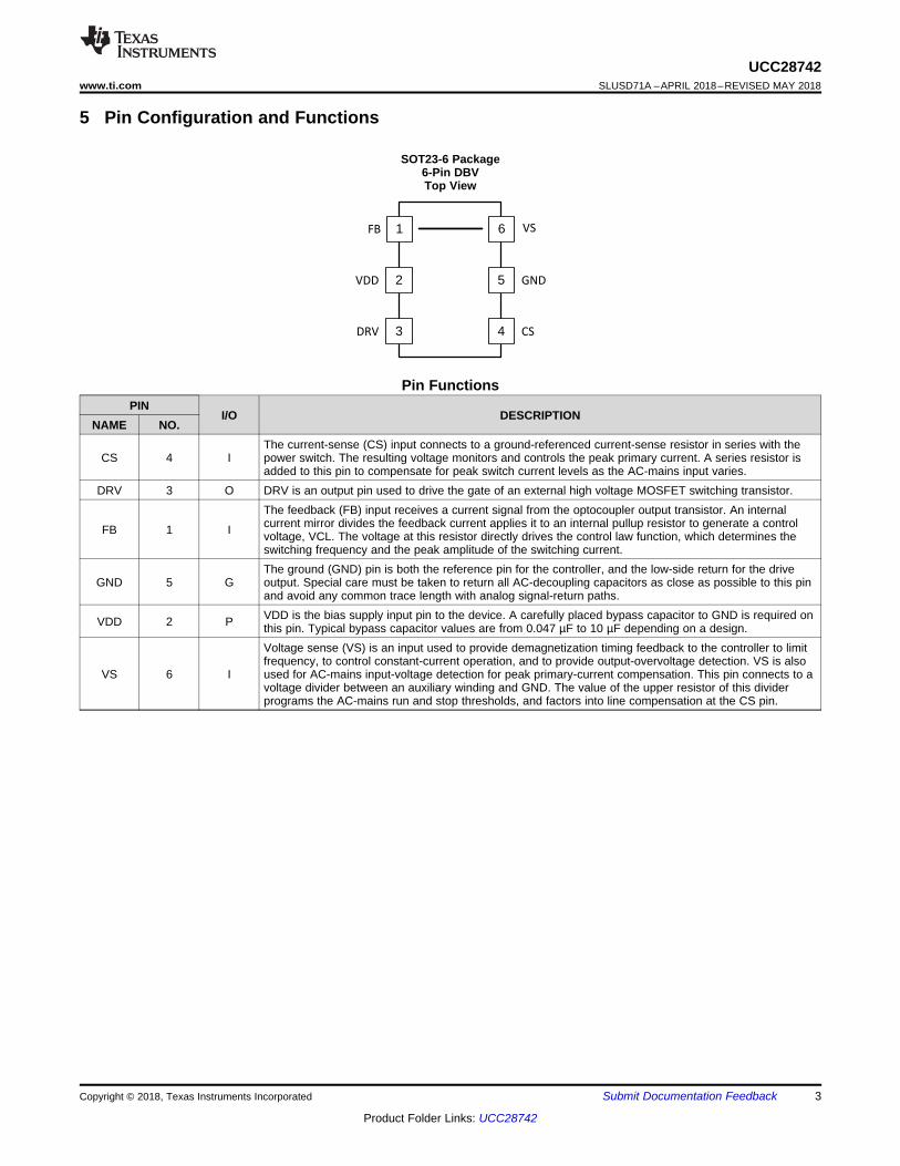
5 Pin Configuration and Functions
SOT23-6 Package6-Pin DBVTop View
Pin FunctionsPIN
I/O DESCRIPTIONNAME NO.
CS 4 IThe current-sense (CS) input connects to a ground-referenced current-sense resistor in series with thepower switch. The resulting voltage monitors and controls the peak primary current. A series resistor isadded to this pin to compensate for peak switch current levels as the AC-mains input varies.
DRV 3 O DRV is an output pin used to drive the gate of an external high voltage MOSFET switching transistor.
FB 1 I
The feedback (FB) input receives a current signal from the optocoupler output transistor. An internalcurrent mirror divides the feedback current applies it to an internal pullup resistor to generate a controlvoltage, VCL. The voltage at this resistor directly drives the control law function, which determines theswitching frequency and the peak amplitude of the switching current.
GND 5 GThe ground (GND) pin is both the reference pin for the controller, and the low-side return for the driveoutput. Special care must be taken to return all AC-decoupling capacitors as close as possible to this pinand avoid any common trace length with analog signal-return paths.
VDD 2 P VDD is the bias supply input pin to the device. A carefully placed bypass capacitor to GND is required onthis pin. Typical bypass capacitor values are from 0.047 µF to 10 µF depending on a design.
VS 6 I
Voltage sense (VS) is an input used to provide demagnetization timing feedback to the controller to limitfrequency, to control constant-current operation, and to provide output-overvoltage detection. VS is alsoused for AC-mains input-voltage detection for peak primary-current compensation. This pin connects to avoltage divider between an auxiliary winding and GND. The value of the upper resistor of this dividerprograms the AC-mains run and stop thresholds, and factors into line compensation at the CS pin.
4
UCC28742SLUSD71A –APRIL 2018–REVISED MAY 2018 www.ti.com
Product Folder Links: UCC28742
Submit Documentation Feedback Copyright © 2018, Texas Instruments Incorporated
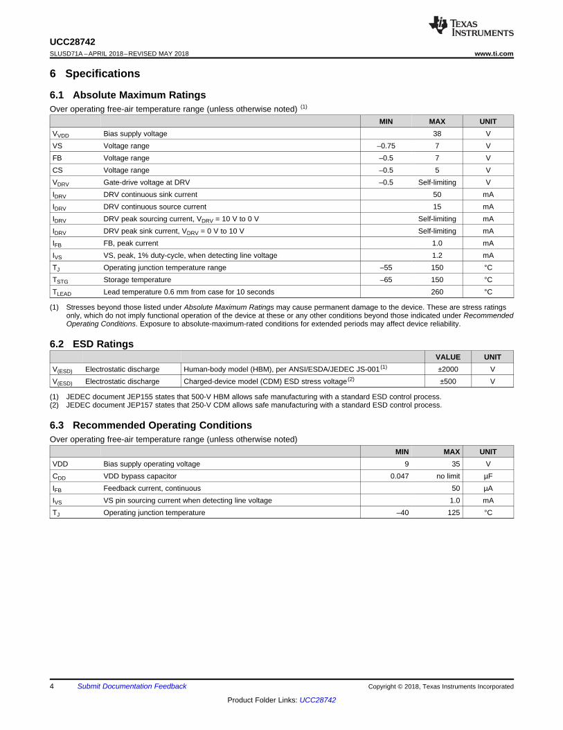
(1) Stresses beyond those listed under Absolute Maximum Ratings may cause permanent damage to the device. These are stress ratingsonly, which do not imply functional operation of the device at these or any other conditions beyond those indicated under RecommendedOperating Conditions. Exposure to absolute-maximum-rated conditions for extended periods may affect device reliability.
6 Specifications
6.1 Absolute Maximum RatingsOver operating free-air temperature range (unless otherwise noted) (1)
MIN MAX UNITVVDD Bias supply voltage 38 VVS Voltage range –0.75 7 VFB Voltage range –0.5 7 VCS Voltage range –0.5 5 VVDRV Gate-drive voltage at DRV –0.5 Self-limiting VIDRV DRV continuous sink current 50 mAIDRV DRV continuous source current 15 mAIDRV DRV peak sourcing current, VDRV = 10 V to 0 V Self-limiting mAIDRV DRV peak sink current, VDRV = 0 V to 10 V Self-limiting mAIFB FB, peak current 1.0 mAIVS VS, peak, 1% duty-cycle, when detecting line voltage 1.2 mATJ Operating junction temperature range –55 150 °CTSTG Storage temperature –65 150 °CTLEAD Lead temperature 0.6 mm from case for 10 seconds 260 °C
(1) JEDEC document JEP155 states that 500-V HBM allows safe manufacturing with a standard ESD control process.(2) JEDEC document JEP157 states that 250-V CDM allows safe manufacturing with a standard ESD control process.
6.2 ESD RatingsVALUE UNIT
V(ESD) Electrostatic discharge Human-body model (HBM), per ANSI/ESDA/JEDEC JS-001 (1) ±2000 VV(ESD) Electrostatic discharge Charged-device model (CDM) ESD stress voltage (2) ±500 V
6.3 Recommended Operating ConditionsOver operating free-air temperature range (unless otherwise noted)
MIN MAX UNITVDD Bias supply operating voltage 9 35 VCDD VDD bypass capacitor 0.047 no limit µFIFB Feedback current, continuous 50 µAIVS VS pin sourcing current when detecting line voltage 1.0 mATJ Operating junction temperature –40 125 °C
5
UCC28742www.ti.com SLUSD71A –APRIL 2018–REVISED MAY 2018
Product Folder Links: UCC28742
Submit Documentation FeedbackCopyright © 2018, Texas Instruments Incorporated
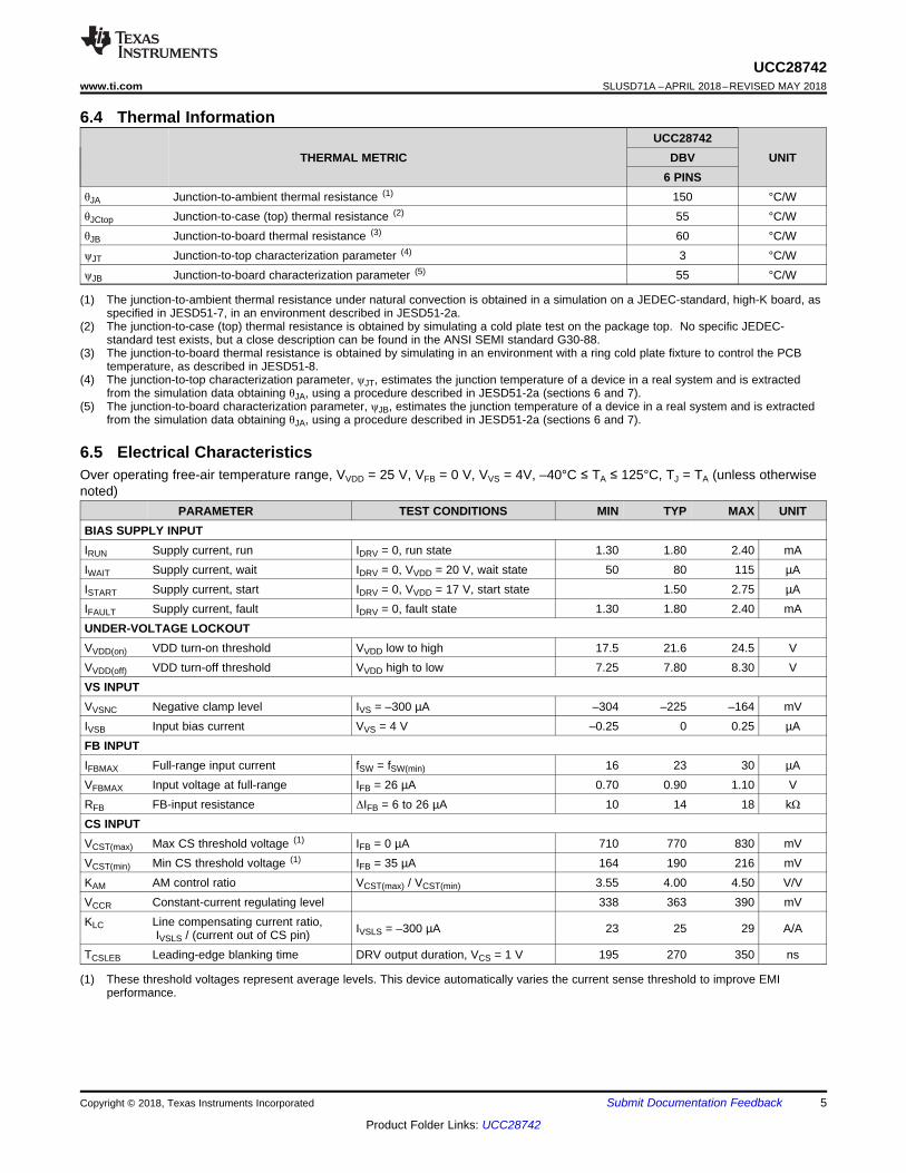
(1) The junction-to-ambient thermal resistance under natural convection is obtained in a simulation on a JEDEC-standard, high-K board, asspecified in JESD51-7, in an environment described in JESD51-2a.
(2) The junction-to-case (top) thermal resistance is obtained by simulating a cold plate test on the package top. No specific JEDEC-standard test exists, but a close description can be found in the ANSI SEMI standard G30-88.
(3) The junction-to-board thermal resistance is obtained by simulating in an environment with a ring cold plate fixture to control the PCBtemperature, as described in JESD51-8.
(4) The junction-to-top characterization parameter, ψJT, estimates the junction temperature of a device in a real system and is extractedfrom the simulation data obtaining θJA, using a procedure described in JESD51-2a (sections 6 and 7).
(5) The junction-to-board characterization parameter, ψJB, estimates the junction temperature of a device in a real system and is extractedfrom the simulation data obtaining θJA, using a procedure described in JESD51-2a (sections 6 and 7).
6.4 Thermal Information
THERMAL METRICUCC28742
UNITDBV6 PINS
θJA Junction-to-ambient thermal resistance (1) 150 °C/WθJCtop Junction-to-case (top) thermal resistance (2) 55 °C/WθJB Junction-to-board thermal resistance (3) 60 °C/WψJT Junction-to-top characterization parameter (4) 3 °C/WψJB Junction-to-board characterization parameter (5) 55 °C/W
(1) These threshold voltages represent average levels. This device automatically varies the current sense threshold to improve EMIperformance.
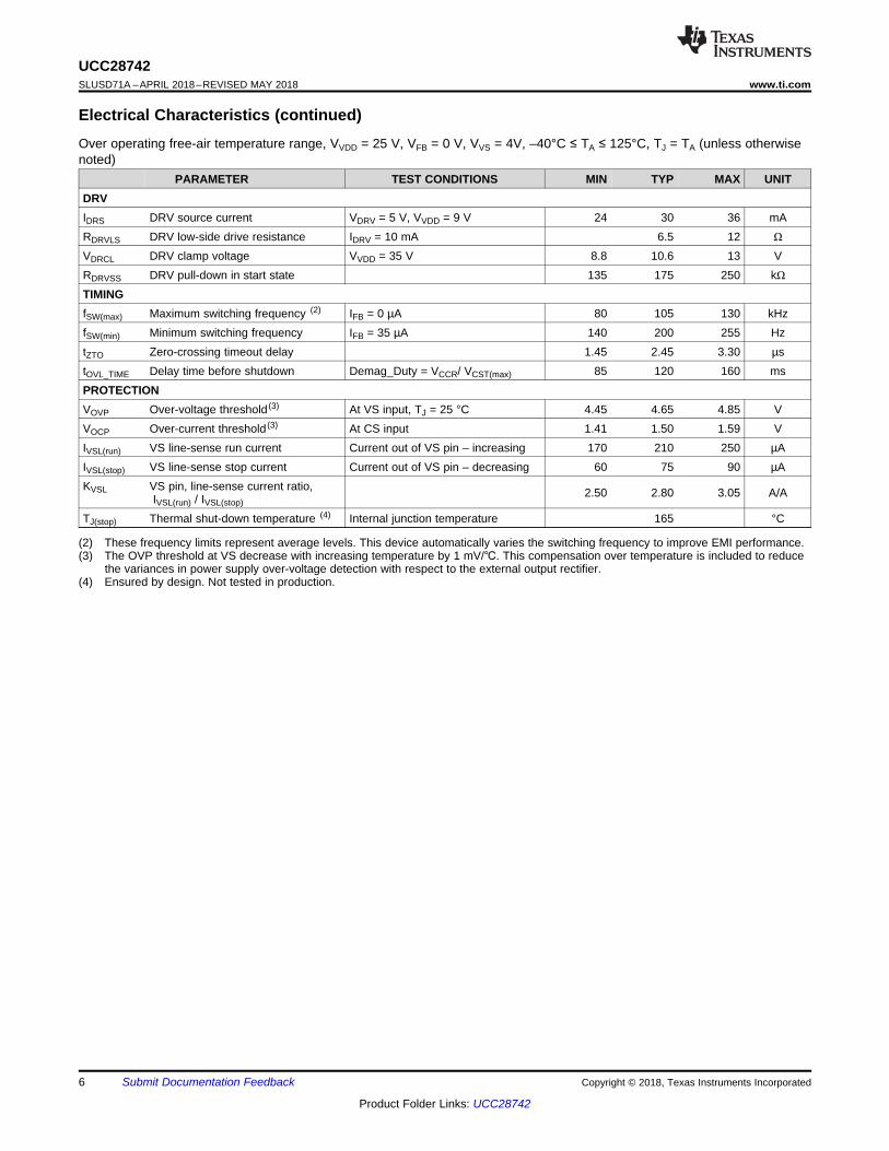
6.5 Electrical CharacteristicsOver operating free-air temperature range, VVDD = 25 V, VFB = 0 V, VVS = 4V, –40°C ≤ TA ≤ 125°C, TJ = TA (unless otherwisenoted)
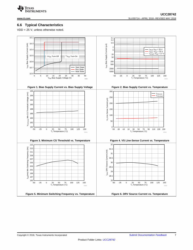
PARAMETER TEST CONDITIONS MIN TYP MAX UNITBIAS SUPPLY INPUTIRUN Supply current, run IDRV = 0, run state 1.30 1.80 2.40 mAIWAIT Supply current, wait IDRV = 0, VVDD = 20 V, wait state 50 80 115 µAISTART Supply current, start IDRV = 0, VVDD = 17 V, start state 1.50 2.75 µAIFAULT Supply current, fault IDRV = 0, fault state 1.30 1.80 2.40 mAUNDER-VOLTAGE LOCKOUTVVDD(on) VDD turn-on threshold VVDD low to high 17.5 21.6 24.5 VVVDD(off) VDD turn-off threshold VVDD high to low 7.25 7.80 8.30 VVS INPUTVVSNC Negative clamp level IVS = –300 µA –304 –225 –164 mVIVSB Input bias current VVS = 4 V –0.25 0 0.25 µAFB INPUTIFBMAX Full-range input current fSW = fSW(min) 16 23 30 µAVFBMAX Input voltage at full-range IFB = 26 µA 0.70 0.90 1.10 VRFB FB-input resistance ΔIFB = 6 to 26 µA 10 14 18 kΩCS INPUTVCST(max) Max CS threshold voltage (1) IFB = 0 µA 710 770 830 mVVCST(min) Min CS threshold voltage (1) IFB = 35 µA 164 190 216 mVKAM AM control ratio VCST(max) / VCST(min) 3.55 4.00 4.50 V/VVCCR Constant-current regulating level 338 363 390 mVKLC Line compensating current ratio,
IVSLS / (current out of CS pin) IVSLS = –300 µA 23 25 29 A/A
TCSLEB Leading-edge blanking time DRV output duration, VCS = 1 V 195 270 350 ns
6
UCC28742SLUSD71A –APRIL 2018–REVISED MAY 2018 www.ti.com
Product Folder Links: UCC28742
Submit Documentation Feedback Copyright © 2018, Texas Instruments Incorporated
Electrical Characteristics (continued)Over operating free-air temperature range, VVDD = 25 V, VFB = 0 V, VVS = 4V, –40°C ≤ TA ≤ 125°C, TJ = TA (unless otherwisenoted)
PARAMETER TEST CONDITIONS MIN TYP MAX UNIT
(2) These frequency limits represent average levels. This device automatically varies the switching frequency to improve EMI performance.(3) The OVP threshold at VS decrease with increasing temperature by 1 mV/. This compensation over temperature is included to reduce
the variances in power supply over-voltage detection with respect to the external output rectifier.(4) Ensured by design. Not tested in production.
DRVIDRS DRV source current VDRV = 5 V, VVDD = 9 V 24 30 36 mARDRVLS DRV low-side drive resistance IDRV = 10 mA 6.5 12 Ω
VDRCL DRV clamp voltage VVDD = 35 V 8.8 10.6 13 VRDRVSS DRV pull-down in start state 135 175 250 kΩTIMINGfSW(max) Maximum switching frequency (2) IFB = 0 µA 80 105 130 kHzfSW(min) Minimum switching frequency IFB = 35 µA 140 200 255 HztZTO Zero-crossing timeout delay 1.45 2.45 3.30 µstOVL_TIME Delay time before shutdown Demag_Duty = VCCR/ VCST(max) 85 120 160 msPROTECTIONVOVP Over-voltage threshold (3) At VS input, TJ = 25 °C 4.45 4.65 4.85 VVOCP Over-current threshold (3) At CS input 1.41 1.50 1.59 VIVSL(run) VS line-sense run current Current out of VS pin – increasing 170 210 250 µAIVSL(stop) VS line-sense stop current Current out of VS pin – decreasing 60 75 90 µAKVSL VS pin, line-sense current ratio,
IVSL(run) / IVSL(stop)2.50 2.80 3.05 A/A
TJ(stop) Thermal shut-down temperature (4) Internal junction temperature 165 °C
TJ Temperature (qC)
f SW
(min
) M
in S
witc
hing
Fre
quen
cy (
Hz)
-50 -25 0 25 50 75 100 125 150195
197
199
201
203
205
207
209
211
213
215
D005TJ Temperature (qC)
I DR
S D
RV
Sou
rce
Cur
rent
(m
A)
-50 -25 0 25 50 75 100 125 15028
28.5
29
29.5
30
30.5
31
31.5
32
D006
TJ Temperature (qC)
VC
ST
(min
) Min
CS
Thr
esho
ld V
olta
ge (
mV
)
-50 -25 0 25 50 75 100 125 150180
182
184
186
188
190
192
194
196
D003 TJ Temperature (qC)
VS L
ine
Sen
se C
urre
nt (P
A)
-50 -30 -10 10 30 50 70 90 110 130 1500
50
100
150
200
250
300
D004
IVSL(run)IVSL(stop)
VDD Bias Supply Voltage (V)
I VD
D B
ias
Sup
ply
Cur
rent
(m
A)
0 5 10 15 20 25 30 35 401E-8
1E-7
1E-6
1E-5
1E-4
1E-3
1E-2
pVDD Turn-Off nVDD Turn-On
D001D001
Start StateRun StateWait State
TJ Temperature (qC)
I VD
D B
ias
Sup
ply
Cur
rent
(P
A)
-50 -25 0 25 50 75 100 125 150
0.10.2
0.5
2
5
20
50
200
500
2000
5000
D002
IRUN VDD = 25 VIWAIT VDD = 20 VISTART VDD = 17 V
7
UCC28742www.ti.com SLUSD71A –APRIL 2018–REVISED MAY 2018
Product Folder Links: UCC28742
Submit Documentation FeedbackCopyright © 2018, Texas Instruments Incorporated
6.6 Typical CharacteristicsVDD = 25 V, unless otherwise noted.
Figure 1. Bias Supply Current vs. Bias Supply Voltage Figure 2. Bias Supply Current vs. Temperature
Figure 3. Minimum CS Threshold vs. Temperature Figure 4. VS Line-Sense Current vs. Temperature
Figure 5. Minimum Switching Frequency vs. Temperature Figure 6. DRV Source Current vs. Temperature
IFB FB Input Current (PA)
VF
B F
B In
put V
olta
ge (
V)
0 5 10 15 20 25 30 35 400
0.1
0.2
0.3
0.4
0.5
0.6
0.7
0.8
0.9
1
1.1
1.2
D007D007 TJ Temperature (qC)
VO
VP M
in C
S T
hres
hold
Vol
tage
(m
V)
-50 -25 0 25 50 75 100 125 1504.4
4.45
4.5
4.55
4.6
4.65
4.7
4.75
4.8
4.85
D008
8
UCC28742SLUSD71A –APRIL 2018–REVISED MAY 2018 www.ti.com
Product Folder Links: UCC28742
Submit Documentation Feedback Copyright © 2018, Texas Instruments Incorporated
Typical Characteristics (continued)VDD = 25 V, unless otherwise noted.
Figure 7. FB Input Voltage vs. FB Input Current Figure 8. VS Overvoltage Threshold vs. Temperature
30 mA
S Q
QR
+
Sampler
Power& Fault
ManagementUVLO
22 V / 7.7 V
ValleySwitching
ControlLaw
VCST
SecondaryTimingDetect
CurrentRegulation
VCST
175 k
VDD
LineSense
+
VOVP
OV FAULT
OV FAULT
IVSLS
+LINE FAULT
LINE FAULT
10 V
2.11 V / 0.75 V
+
1.5 VOC FAULT
OC FAULT
IVSLS / KLCIVSLS
5 V
5 V
1 / fSW
LEB
VCLIFB / 2.5
IFB
0.55 V
+/VCST(max)
0.475
VCCR
OVL FAULT
480 N
14 N
120 ms Delay
GND
VDD
FB
VS
10 k
GND
DRV
CS
9
UCC28742www.ti.com SLUSD71A –APRIL 2018–REVISED MAY 2018
Product Folder Links: UCC28742
Submit Documentation FeedbackCopyright © 2018, Texas Instruments Incorporated
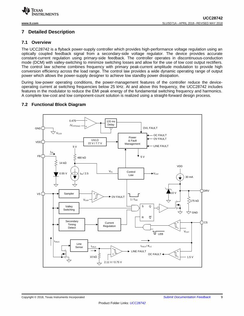
7 Detailed Description
7.1 OverviewThe UCC28742 is a flyback power-supply controller which provides high-performance voltage regulation using anoptically coupled feedback signal from a secondary-side voltage regulator. The device provides accurateconstant-current regulation using primary-side feedback. The controller operates in discontinuous-conductionmode (DCM) with valley-switching to minimize switching losses and allow for the use of low cost output rectifiers.The control law scheme combines frequency with primary peak-current amplitude modulation to provide highconversion efficiency across the load range. The control law provides a wide dynamic operating range of outputpower which allows the power-supply designer to achieve low standby power dissipation.
During low-power operating conditions, the power-management features of the controller reduce the device-operating current at switching frequencies below 25 kHz. At and above this frequency, the UCC28742 includesfeatures in the modulator to reduce the EMI peak energy of the fundamental switching frequency and harmonics.A complete low-cost and low component-count solution is realized using a straight-forward design process.
7.2 Functional Block Diagram
10
UCC28742SLUSD71A –APRIL 2018–REVISED MAY 2018 www.ti.com
Product Folder Links: UCC28742
Submit Documentation Feedback Copyright © 2018, Texas Instruments Incorporated
7.3 Feature Description
7.3.1 Detailed Pin Description
7.3.1.1 VDD (Device Bias Voltage Supply)The VDD pin is typically powered from a rectified auxiliary transformer winding, the same winding that is used tocapture the output voltage level. A bypass capacitor, with minimum value 0.047 μF, on the VDD pin is used forinitially biasing the device to start-up along with a resistive or active source of start-up charging current. UVLOstart / stop levels of 21.6 V / 7.8 V accommodate lower values of VDD capacitance that in turns keeps the start-up current low, which for resistive start-up has an impact on both stand-by power and power-on delay. A high,35-V, maximum operating level on VDD alleviates concerns with leakage energy charging of VDD and givesadded flexibility to when varying power supply output voltage must be supported.
7.3.1.2 GND (Ground)This is an external return pin, and provides the reference point for both external signal and the gate drive of thedevice. The VDD bypass capacitor should be placed close to this pin. Critical component GND connections fromthe VS, FB and CS pins should have dedicated and short paths to this pin.
u
u
S1 OVPS2
AS OV F OVP
R VR
N (V V ) V
IN(run) BULK(run)
S1PA VSL(run) PA VSL(run)
2 V VR
N I N I
u
|u u
11
UCC28742www.ti.com SLUSD71A –APRIL 2018–REVISED MAY 2018
Product Folder Links: UCC28742
Submit Documentation FeedbackCopyright © 2018, Texas Instruments Incorporated
Feature Description (continued)7.3.1.3 VS (Voltage-Sense)The VS pin connects to a resistor-divider from the auxiliary winding to ground. The auxiliary voltage waveform issampled at the end of the transformer secondary-current demagnetization time. The waveform on the VS pindetermines (1) the timing information to achieve valley-switching, (2) the timing to control the duty-cycle of thetransformer secondary current, and (3) the output voltage over-voltage. Avoid placing a filter capacitor on thisinput which interferes with accurate sensing of this waveform.
Besides, the VS pin also has these two functions: (4) senses the bulk capacitor input voltage to provide for ac-input run and stop thresholds, and (5) to compensate the current-sense threshold across the AC-input range.This information is sensed by monitoring the current pulled out of the VS pin during the MOSFET on-time. Duringthis time the voltage on the VS pin is clamped to about 250 mV below GND. As a result, the current out of thepin is determined by the upper VS divider resistor, the auxiliary to primary turns-ratio and the bulk input voltagelevel. For the AC-input run/stop function, the run threshold on VS is IVSL(run) (typical 210 µA) and the stopthreshold is IVSL(stop) (typical 75 µA). The values for the auxiliary voltage divider upper-resistor RS1 and lower-resistor RS2 can be determined by the equations below.
where• NPA is the transformer primary-to-auxiliary turns ratio,• VIN(run) is the AC rms voltage to enable turn-on of the flyback converter (run),• VBULK(run) is the DC bulk voltage to enable turn-on of the flyback converter (run),• IVSL(run) is the run-threshold for the current pulled out of the VS pin during the primary MOSFET on-time. (see
the Electrical Characteristics table). (1)
where• VOV is the maximum allowable peak voltage at the converter output,• VF is the output rectifier forward voltage drop at near-zero current,• NAS is the transformer auxiliary to secondary turns ratio,• RS1 is the VS divider upper-resistor resistance,• VOVP is the overvoltage detection threshold at the VS input (see the Electrical Characteristics table). (2)
Notice that VS pin absolute maximum current IVS in its negative clamping is 1.2 mA. After determined RS1 it isrequired to check if VS pin current stays ≤ 1.2 mA. The check is to determine the input voltage ratio in this designand make VIN(max) / VIN(run) ≤ IVS / IVSL(run) = 1.2 mA / 0.25 mA = 4.8, i.e., VIN(max) / VIN(run) ≤ 4.8. If the designcannot meet this criterion, external circuit is needed to add in to make sure VS pin current ≤ 1.2 mA, for example,to use a zener type of device to clamp the transformer aux-winding negative voltage to achieve VIN(max) / VIN(run) ≤4.8.
7.3.1.4 DRV (Gate Drive)The DRV pin is connected to the MOSFET gate pin, usually through a series resistor. The DRV provides a gatedrive signal which is clamped to 10-V internally. During turn-on the driver applies a typical 30-mA current sourceout of the DRV pin. When the DRV voltage rises to above 9 V the output current is reduced to about 100 µA.This current brings the DRV voltage to the 10-V clamp level, or to VDD, whichever is less. The 30-mA currentprovides adequate turn-on speed while automatically limiting noise generated at turn-on by the MOSFET draindv/dt and by the leading edge turn-on current spike. The gate drive turn-off current is internally limited to about400 mA when DRV is above about 4 V. At lower DRV voltages the current will reduce, eventually being limitedby the low-side on resistance, RDS(on). The drain turn-on and turn-off dv/dt can be further impacted by addingexternal resistor in series with DRV pin. The drain current resonances can be damped with a small series gateresistor, generally less than a 1 Ω.
LC S1 CS D GATE _ OFF PALC
P
K R R (t t ) NR
L
u u u u
CCR PSCS XFMR
OCC
V NR
2 I
u u K
u
12
UCC28742SLUSD71A –APRIL 2018–REVISED MAY 2018 www.ti.com
Product Folder Links: UCC28742
Submit Documentation Feedback Copyright © 2018, Texas Instruments Incorporated
Feature Description (continued)7.3.1.5 CS (Current Sense)The current sense pin is connected through a series resistor (RLC) to the current-sense resistor (RCS). Thecontroller varies the internal current sense threshold between 190 mV and 770 mV, setting a correspondingcontrol range for the peak-primary winding current to a 4-to-1 range. The series resistor RLC provides an inputvoltage feed-forward function. The voltage drop across this resistor reduces primary-side peak current as the linevoltage increases, compensating for the increased di/dt and delays in the MOSFET turn-off. There is an internalleading-edge blanking time of 270 ns to eliminate sensitivity to the MOSFET turn-on leading edge current spike.If additional blanking time is needed, a small bypass capacitor, up to 30 pF, can be placed on between CS pinand GND pin. The value of RCS is determined by the target output current in constant current (CC) regulation.The values of RCS and RLC can be determined by the equations below. The term ηXFMR is intended to account forthe energy stored in the transformer but not delivered to the secondary. This includes transformer core andcopper losses, bias power, and primary leakage inductance losses.
Example: With a transformer core and copper losses of 3%, leakage inductance caused power losses 2%, andbias power to output power ratio of 0.5%. The transformer power transfer efficiency is estimated as ηXFMR =100% - 3% - 2% - 0.5% = 94.5%
where• VCCR is a current regulation constant (see the Electrical Characteristics table),• NPS is the transformer primary-to-secondary turns ratio (a typical turns-ratio of 12 to 15 is recommended for 5-
V output as an example),• IOCC is the target output current in constant-current limit (refer to Constant Current Limit and Delayed
Shutdown for more detail),• ηXFMR is the transformer efficiency. (3)
where• RS1 is the VS pin high-side resistor value,• RCS is the current-sense resistor value,• tD is the current-sense delay (typical 50 ns) plus MOSFET turn-off delay,• tGATE_OFF is the primary-side main MOSFET turn-off time,• NPA is the transformer primary-to-auxiliary turns-ratio,• LP is the transformer primary inductance,• KLC is a current-scaling constant (see the Electrical Characteristics table). (4)
7.3.1.6 FB (Feedback)The FB pin connects to the emitter of an analog optocoupler output transistor which usually has the collectorconnected to VDD. The current supplied to FB by the optocoupler is reduced internally by a factor of 2.5 and theresulting current is applied to an internal 480-kΩ resistor to generate the control law voltage (VCL). This VCLdirectly determines the converter switching frequency and peak primary current required for regulation per thecontrol-law for any given line and load condition.
Typical circuit connection between FB and optocoupler along with typical values of resistors and capacitorsshould be made as shown in Figure 9. The resistors and capacitors in the connections help to stabilize operationduring control mode transition.
(VOUT + VF + ISRS) NA / NS
- (VBLK) NA / NP
0 V
VS Sample
Auxiliary
VSDiscriminator &
Sampler
Timing
ControlLaw²
MinimumPeriod
And Peak Primary Current
CS
Zero Crossings
VCL
Mirror
Network
VDD
+ VREF
-
IOPT
VOUT
Secondary
+ VF - VBULK
+Primary
IFB
RCS
GD DRV
RFP
FBRFS
CFS
ROPT
RS1
RS2
GND
ZFBRFB1
RFB2
COUT RLOAD
RTL
13
UCC28742www.ti.com SLUSD71A –APRIL 2018–REVISED MAY 2018
Product Folder Links: UCC28742
Submit Documentation FeedbackCopyright © 2018, Texas Instruments Incorporated
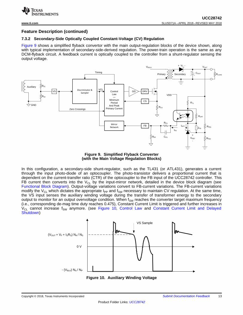
Feature Description (continued)7.3.2 Secondary-Side Optically Coupled Constant-Voltage (CV) RegulationFigure 9 shows a simplified flyback convertor with the main output-regulation blocks of the device shown, alongwith typical implementation of secondary-side-derived regulation. The power-train operation is the same as anyDCM-flyback circuit. A feedback current is optically coupled to the controller from a shunt-regulator sensing theoutput voltage.
Figure 9. Simplified Flyback Converter(with the Main Voltage Regulation Blocks)
In this configuration, a secondary-side shunt-regulator, such as the TL431 (or ATL431), generates a currentthrough the input photo-diode of an optocoupler. The photo-transistor delivers a proportional current that isdependent on the current-transfer ratio (CTR) of the optocoupler to the FB input of the UCC28742 controller. ThisFB current then converts into the VCL by the input-mirror network, detailed in the device block diagram (seeFunctional Block Diagram). Output-voltage variations convert to FB-current variations. The FB-current variationsmodify the VCL which dictates the appropriate IPP and fSW necessary to maintain CV regulation. At the same time,the VS input senses the auxiliary winding voltage during the transfer of transformer energy to the secondaryoutput to monitor for an output overvoltage condition. When fSW reaches the converter target maximum frequency(i.e., corresponding de-mag time duty reaches 0.475), Constant Current Limit is triggered and further increases inVCL cannot increase fSW anymore. (see Figure 10, Control Law and Constant Current Limit and DelayedShutdown)
Figure 10. Auxiliary Winding Voltage
0 V
VS ring p-p(scaled)
tDM_BLANK
tLK RESET
tDMAG
tSW
(QWHULQJ³:DLW´6WDWH
Ipp < Ipp(max)
RS2/(RS1+RS2)
14
UCC28742SLUSD71A –APRIL 2018–REVISED MAY 2018 www.ti.com
Product Folder Links: UCC28742
Submit Documentation Feedback Copyright © 2018, Texas Instruments Incorporated
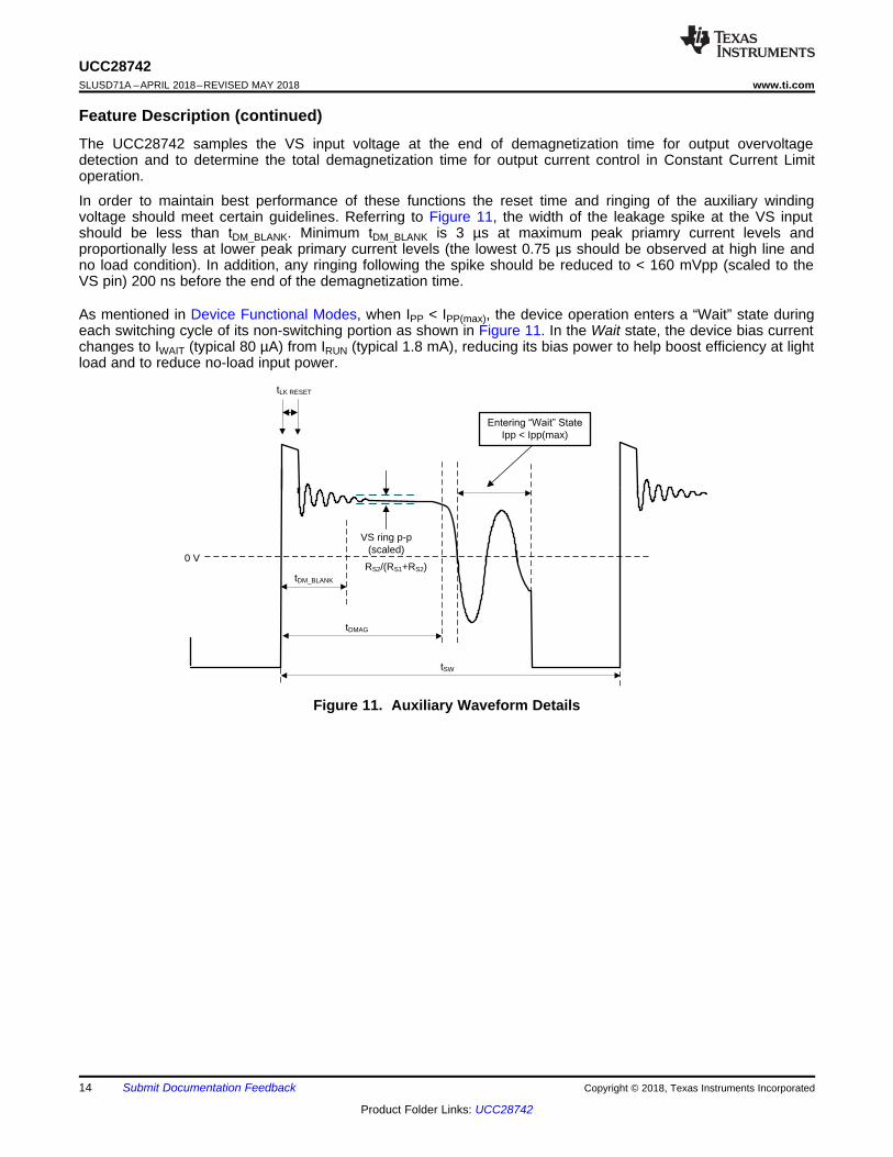
Feature Description (continued)The UCC28742 samples the VS input voltage at the end of demagnetization time for output overvoltagedetection and to determine the total demagnetization time for output current control in Constant Current Limitoperation.
In order to maintain best performance of these functions the reset time and ringing of the auxiliary windingvoltage should meet certain guidelines. Referring to Figure 11, the width of the leakage spike at the VS inputshould be less than tDM_BLANK. Minimum tDM_BLANK is 3 µs at maximum peak priamry current levels andproportionally less at lower peak primary current levels (the lowest 0.75 µs should be observed at high line andno load condition). In addition, any ringing following the spike should be reduced to < 160 mVpp (scaled to theVS pin) 200 ns before the end of the demagnetization time.
As mentioned in Device Functional Modes, when IPP < IPP(max), the device operation enters a “Wait” state duringeach switching cycle of its non-switching portion as shown in Figure 11. In the Wait state, the device bias currentchanges to IWAIT (typical 80 µA) from IRUN (typical 1.8 mA), reducing its bias power to help boost efficiency at lightload and to reduce no-load input power.
Figure 11. Auxiliary Waveform Details
Control Law Voltage, Internal - VCL
Control-Law Profile in Constant-Voltage (CV) Mode
f SW
I PP (
peak
prim
ary
curr
ent)
5 V3.2 V2.2 V1.3 V0.75 V
IPP(max)
105 kHz
200 Hz
fSW
IPP
IPP(max) / 4
25 kHz
3.80 kHz
AMFM 1 FM 3
0 V
Corresponding Feed-back Current, FB Input - IFB
0.5 µA9.4 µA14.6 µA19.3 µA22.1 µA26 µA
4.9 V
FM 2
15
UCC28742www.ti.com SLUSD71A –APRIL 2018–REVISED MAY 2018
Product Folder Links: UCC28742
Submit Documentation FeedbackCopyright © 2018, Texas Instruments Incorporated
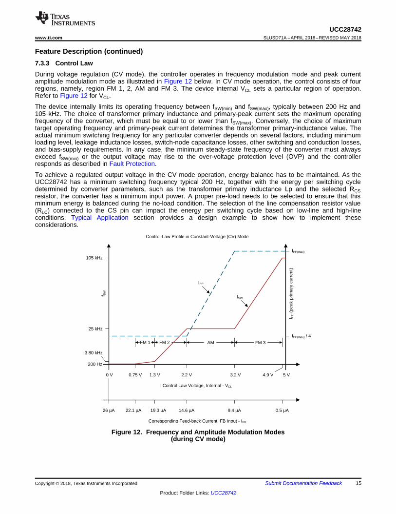
Feature Description (continued)7.3.3 Control LawDuring voltage regulation (CV mode), the controller operates in frequency modulation mode and peak currentamplitude modulation mode as illustrated in Figure 12 below. In CV mode operation, the control consists of fourregions, namely, region FM 1, 2, AM and FM 3. The device internal VCL sets a particular region of operation.Refer to Figure 12 for VCL.
The device internally limits its operating frequency between fSW(min) and fSW(max), typically between 200 Hz and105 kHz. The choice of transformer primary inductance and primary-peak current sets the maximum operatingfrequency of the converter, which must be equal to or lower than fSW(max). Conversely, the choice of maximumtarget operating frequency and primary-peak current determines the transformer primary-inductance value. Theactual minimum switching frequency for any particular converter depends on several factors, including minimumloading level, leakage inductance losses, switch-node capacitance losses, other switching and conduction losses,and bias-supply requirements. In any case, the minimum steady-state frequency of the converter must alwaysexceed fSW(min) or the output voltage may rise to the over-voltage protection level (OVP) and the controllerresponds as described in Fault Protection.
To achieve a regulated output voltage in the CV mode operation, energy balance has to be maintained. As theUCC28742 has a minimum switching frequency typical 200 Hz, together with the energy per switching cycledetermined by converter parameters, such as the transformer primary inductance Lp and the selected RCSresistor, the converter has a minimum input power. A proper pre-load needs to be selected to ensure that thisminimum energy is balanced during the no-load condition. The selection of the line compensation resistor value(RLC) connected to the CS pin can impact the energy per switching cycle based on low-line and high-lineconditions. Typical Application section provides a design example to show how to implement theseconsiderations.
Figure 12. Frequency and Amplitude Modulation Modes(during CV mode)
tON tDMAG
tSW
IPP ISP x NS/NP
t
i
DMAGPP POUT
S SW
tI NI
2 N t u u
16
UCC28742SLUSD71A –APRIL 2018–REVISED MAY 2018 www.ti.com
Product Folder Links: UCC28742
Submit Documentation Feedback Copyright © 2018, Texas Instruments Incorporated
Feature Description (continued)The steady-state control-law voltage, VCL, ranges between 0.75 V to 4.90 V. Heavy load operation is usually inRegion FM 3 where frequency modulation to output regulation is used and primary-peak current is controlled atits maximum. The AM region is usually for medium-load range typically from 10% load and above. In this regionswitching frequency is fixed at nominal 25 kHz along with primary-peak current varying from 25% to 100% of itsmaximum. The low operating frequency ranges are for lighter loads to achieve stable regulation at lowfrequencies. In regions FM 1 and 2, peak-primary current is always maintained at IPP(max)/4. Transitions betweenlevels are automatically accomplished by the controller depending on the internal control-law voltage, VCL and itscorresponding FB pin current IFB. An internal frequency-dithering mechanism is enabled in Region FM 3 toreduce conducted EMI, and is disabled otherwise. The Wait state is enabled in regions FM 1, 2, and AM, refer toFigure 11.
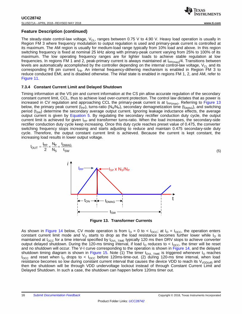
7.3.4 Constant Current Limit and Delayed ShutdownTiming information at the VS pin and current information at the CS pin allow accurate regulation of the secondaryconstant current limit, CCL, thus to achieve load over-current protection. The control law dictates that as power isincreased in CV regulation and approaching CCL the primary-peak current is at IPP(max). Referring to Figure 13below, the primary peak current (IPP), turns-ratio (NS/NP), secondary demagnetization time (tDMAG), and switchingperiod (tSW) determine the secondary average output current. Ignoring leakage inductance effects, the averageoutput current is given by Equation 5. By regulating the secondary rectifier conduction duty cycle, the outputcurrent limit is achieved for given IPP and transformer turns-ratio. When the load increases, the secondary-siderectifier conduction duty cycle keep increasing. Once this duty cycle reaches preset value of 0.475, the converterswitching frequency stops increasing and starts adjusting to reduce and maintain 0.475 secondary-side dutycycle. Therefore, the output constant current limit is achieved. Because the current is kept constant, theincreasing load results in lower output voltage.
(5)
Figure 13. Transformer Currents
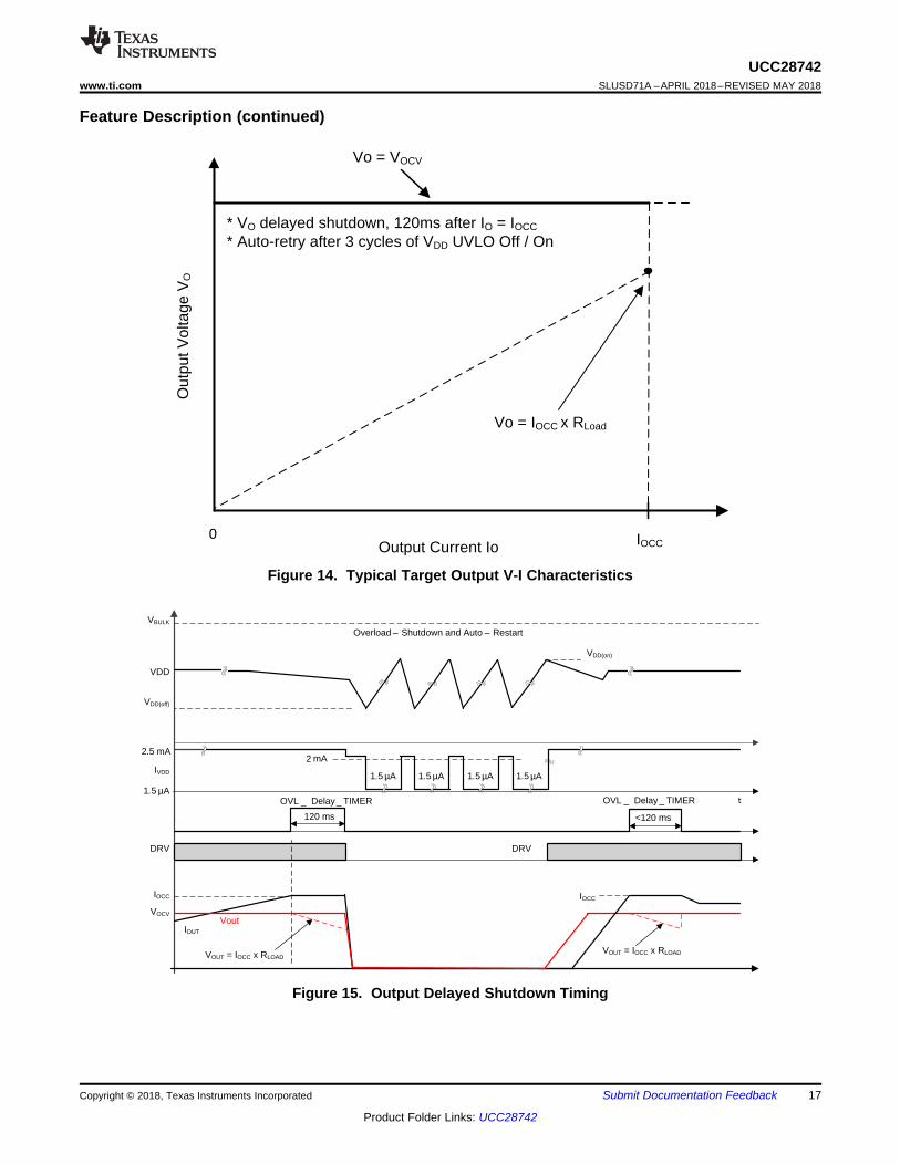
As shown in Figure 14 below, CV mode operation is from IO = 0 to < IOCC; at IO = IOCC, the operation entersconstant current limit mode and VO starts to drop as the load resistance becomes further lower while IO ismaintained at IOCC for a time interval specified by tOVL_TIME typically 120 ms then DRV stops to achieve converteroutput delayed shutdown. During the 120-ms timing interval, if load IO reduces to < IOCC, the timer will be resetand no shutdown will occur. The V-I curve corresponding to the operation is shown in Figure 14, and the delayedshutdown timing diagram is shown in Figure 15. Note (1) The timer tOVL_TIME is triggered whenever IO reachesIOCC and reset when IO drops to < IOCC before 120ms-time-out. (2) during 120-ms time interval, when loadresistance becomes so low during constant current interval that causes the device VDD to reach its VVDD(off) andthen the shutdown will be through VDD undervoltage lockout instead of through Constant Current Limit andDelayed Shutdown. In such a case, the shutdown can happen before 120ms timer out.
VDD
IVDD
DRV
120 ms
Vout
IOCC
IOUT
VBULK
DRV
Overload ± Shutdown and Auto ± Restart
VOCV
t
VDD(off)
2 mA
.1 5 µA .1 5 µA .1 5 µA .1 5 µA
.1 5 µAOVL _ Delay_ TIMER
2.5 mA
<120 ms
OVL _ Delay_ TIMER
VDD(on)
IOCC
VOUT = IOCC x RLOADVOUT = IOCC x RLOAD
0 IOCC
Out
put V
olta
ge V
O
Output Current Io
* VO delayed shutdown, 120ms after IO = IOCC * Auto-retry after 3 cycles of VDD UVLO Off / On
Vo = IOCC x RLoad
Vo = VOCV
17
UCC28742www.ti.com SLUSD71A –APRIL 2018–REVISED MAY 2018
Product Folder Links: UCC28742
Submit Documentation FeedbackCopyright © 2018, Texas Instruments Incorporated
Feature Description (continued)
Figure 14. Typical Target Output V-I Characteristics
Figure 15. Output Delayed Shutdown Timing
VDS
VDRV
t
0 V
0 V
18
UCC28742SLUSD71A –APRIL 2018–REVISED MAY 2018 www.ti.com
Product Folder Links: UCC28742
Submit Documentation Feedback Copyright © 2018, Texas Instruments Incorporated
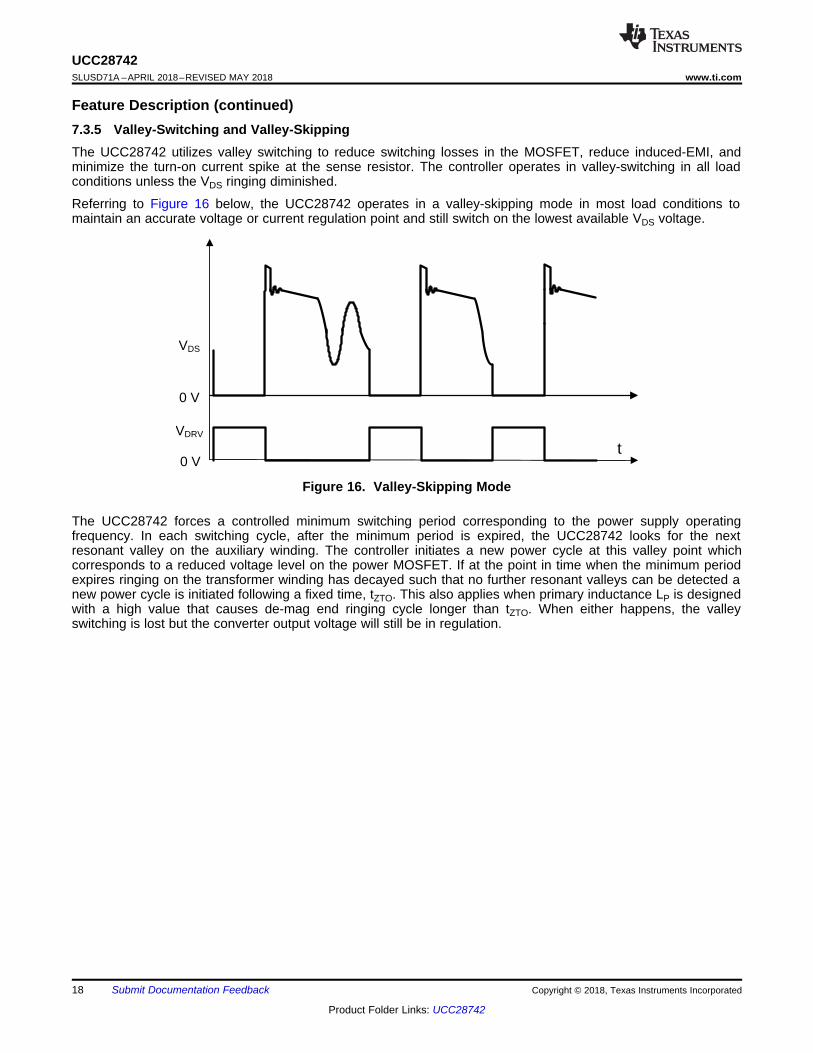
Feature Description (continued)7.3.5 Valley-Switching and Valley-SkippingThe UCC28742 utilizes valley switching to reduce switching losses in the MOSFET, reduce induced-EMI, andminimize the turn-on current spike at the sense resistor. The controller operates in valley-switching in all loadconditions unless the VDS ringing diminished.
Referring to Figure 16 below, the UCC28742 operates in a valley-skipping mode in most load conditions tomaintain an accurate voltage or current regulation point and still switch on the lowest available VDS voltage.
Figure 16. Valley-Skipping Mode
The UCC28742 forces a controlled minimum switching period corresponding to the power supply operatingfrequency. In each switching cycle, after the minimum period is expired, the UCC28742 looks for the nextresonant valley on the auxiliary winding. The controller initiates a new power cycle at this valley point whichcorresponds to a reduced voltage level on the power MOSFET. If at the point in time when the minimum periodexpires ringing on the transformer winding has decayed such that no further resonant valleys can be detected anew power cycle is initiated following a fixed time, tZTO. This also applies when primary inductance LP is designedwith a high value that causes de-mag end ringing cycle longer than tZTO. When either happens, the valleyswitching is lost but the converter output voltage will still be in regulation.
UCC28742SOT23-6
DRV
CS
VDD
GND
VS
NP NS
NA
VAUX
VAC
FB
+
±
ZFB
IFB
+ VFA -
IOPT
VVDD
RFB4
RFB3
VE
CFB3
CVDD
RTL
RFB2
RFB1
ROPT
COUT
RCS
RLC
RS2
RS1
RSTR
CB2CB1
+ VF -VOUT
VBULK
19
UCC28742www.ti.com SLUSD71A –APRIL 2018–REVISED MAY 2018
Product Folder Links: UCC28742
Submit Documentation FeedbackCopyright © 2018, Texas Instruments Incorporated
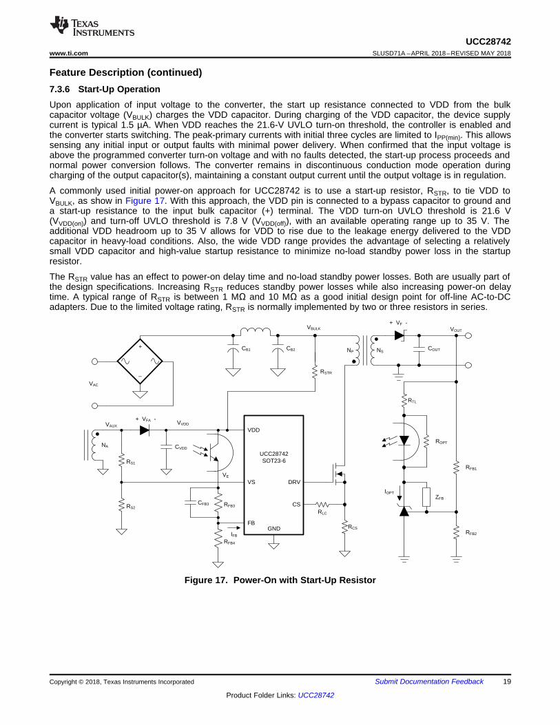
Feature Description (continued)7.3.6 Start-Up OperationUpon application of input voltage to the converter, the start up resistance connected to VDD from the bulkcapacitor voltage (VBULK) charges the VDD capacitor. During charging of the VDD capacitor, the device supplycurrent is typical 1.5 µA. When VDD reaches the 21.6-V UVLO turn-on threshold, the controller is enabled andthe converter starts switching. The peak-primary currents with initial three cycles are limited to IPP(min). This allowssensing any initial input or output faults with minimal power delivery. When confirmed that the input voltage isabove the programmed converter turn-on voltage and with no faults detected, the start-up process proceeds andnormal power conversion follows. The converter remains in discontinuous conduction mode operation duringcharging of the output capacitor(s), maintaining a constant output current until the output voltage is in regulation.
A commonly used initial power-on approach for UCC28742 is to use a start-up resistor, RSTR, to tie VDD toVBULK, as show in Figure 17. With this approach, the VDD pin is connected to a bypass capacitor to ground anda start-up resistance to the input bulk capacitor (+) terminal. The VDD turn-on UVLO threshold is 21.6 V(VVDD(on)) and turn-off UVLO threshold is 7.8 V (VVDD(off)), with an available operating range up to 35 V. Theadditional VDD headroom up to 35 V allows for VDD to rise due to the leakage energy delivered to the VDDcapacitor in heavy-load conditions. Also, the wide VDD range provides the advantage of selecting a relativelysmall VDD capacitor and high-value startup resistance to minimize no-load standby power loss in the startupresistor.
The RSTR value has an effect to power-on delay time and no-load standby power losses. Both are usually part ofthe design specifications. Increasing RSTR reduces standby power losses while also increasing power-on delaytime. A typical range of RSTR is between 1 MΩ and 10 MΩ as a good initial design point for off-line AC-to-DCadapters. Due to the limited voltage rating, RSTR is normally implemented by two or three resistors in series.
Figure 17. Power-On with Start-Up Resistor
20
UCC28742SLUSD71A –APRIL 2018–REVISED MAY 2018 www.ti.com
Product Folder Links: UCC28742
Submit Documentation Feedback Copyright © 2018, Texas Instruments Incorporated
Feature Description (continued)7.3.7 Fault ProtectionThere is comprehensive fault protection incorporated into the UCC28742. Protection functions include:• Output Over-Voltage• Input Under-Voltage• Primary Over-Current Fault• CS Pin Open Fault• CS Pin Short-to-GND Fault• VS Pin Fault• Device Internal Over-Temperature• Constant Current Limit and Delayed Output Shutdown - Output Over-Current Protection
Output Over-Voltage: The output over-voltage function is determined by the voltage feedback on the VS pin. Ifthe voltage sample on VS exceeds 4.65 V (VOVP), for three consecutive switching cycles an OV fault is asserted.Once asserted the device stops switching, initiating a UVLO reset and re-start fault cycle. During the fault, theVDD bias current remains at the run current level, discharging the VDD pin to the UVLO turn-off threshold,VVDD(off). After that, the device returns to the start state, VDD now charging to VVDD(on) where switching isinitiated. The UVLO sequence repeats as long as the fault condition persists.
Input Under-Voltage: The line input run and stop thresholds are determined by current information at the VS pinduring the MOSFET on-time. While the VS pin is clamped close to GND during the MOSFET on-time, the currentthrough RS1, out of the VS pin, is monitored to determine a sample of the bulk capacitor voltage. A wideseparation of run and stop thresholds allows clean start-up and shut-down of the power supply with the linevoltage. From the start state, the sensed VS current, IVSL, must exceed the run current threshold, IVSL(run) (typical211 µA), within the first three cycles after switching starts as VDD reaches VVDD(on). If it does not, then switchingstops and the UVLO reset and re-start fault cycle is initiated. Once running, IVSL must drop below the stop level,IVSL(stop) (typically 75 µA), for three consecutive cycles to initiate the fault response.
Primary Over-Current: The UCC28742 always operates with cycle-by-cycle primary-peak current control. Thenormal operating range of the CS pin is 190 mV to 770 mV. If the voltage on CS exceeds the 1.5-V over-currentlevel, any time after the internal leading edge blanking time and before the end of the transformerdemagnetization, for three consecutive cycles, the device shuts down and the UVLO reset and re-start fault cyclebegins.
CS Pin Open: The CS pin has a 2-µA minimum pull-up that brings the CS pin above the 1.5-V OC fault level ifthe CS pin is open. This causes the primary over-current fault after three cycles.
CS Pin Short to GND: On the first, and only the first, cycle at start-up during power on, the device checks toverify that the VCST(min) threshold is reached at the CS pin within 5 µs of DRV going high. If the CS voltage fails toreach this level then the device terminates the current cycle and immediately enters the UVLO reset and re-startfault sequence.
VS Pin: Protection is included in the event of component failures on the VS pin. If the high-side VS dividerresistor opens the controller stops switching. VDD collapses to its VVDD(off) threshold, a start-up attempt followswith a single DRV on-time when VDD reaches VVDD(on). The UVLO cycle will repeat. If the low-side VS dividerresistor is open then an output over-voltage fault occurs.
Device Internal OTP: The internal over-temperature protection threshold is 165 °C. If the junction temperature ofthe device reaches this threshold the device initiates the UVLO reset and re-start fault cycle. If the temperature isstill high at the end of the UVLO cycle, the protection cycle repeats.
Constant Current Limit and Delayed Output Shutdown - Output Over-Current Protection: The load over-current protection is made precisely using constant current limit and delayed output shutdown as described insection Constant Current Limit and Delayed Shutdown
21
UCC28742www.ti.com SLUSD71A –APRIL 2018–REVISED MAY 2018
Product Folder Links: UCC28742
Submit Documentation FeedbackCopyright © 2018, Texas Instruments Incorporated
7.4 Device Functional ModesThe UCC28742 operates in different modes according to input voltage, VDD voltage, and output load conditions:• At start-up, when VDD is less than the turn-on threshold, VVDD(on) , the device is simply waiting for VDD to
reach this threshold while the VDD capacitor is getting charged.• When VDD exceeds VVDD(on), the device starts switching to deliver power to the converter output. The initial 3
switching cycles control the primary-peak current to IPP(min). This allows sensing any initial input or outputfaults with minimal power delivery. When confirmed with input voltage above predetermined level and no faultconditions, start up process proceeds and normal power conversion follows. The converter will remain indiscontinuous current mode operation during charging of the output capacitor(s), maintaining a constantoutput current, IOCC, until the output voltage reaches its regulation point. The maximum time duration when IOstays on IOCC can only last 120 ms, and when 120-ms timer out, the device will initiate shutdown. Therefore, adesign needs to make sure the maximum time when output current reaches and stays on IOCC does notexceed 120 ms during start. For more details refer to Constant Current Limit and Delayed Shutdown
• When operating with IPP = IPP(max), the UCC28742 operates continuously in the run state. In this state, theVDD bias current is always at IRUN plus the average gate-drive current.
• When operating with IPP < IPP(max), the UCC28742 operates in the wait state between switching cycles and inthe run state during a switching cycle. In the wait state, the VDD bias current is reduced to IWAIT afterdemagnetizing time of each switching cycle to improve efficiency at light loads. This helps reduce no-load tomedium-load power losses, particularly for achieving higher efficiency at 10%, 25% load conditions, andpossible at < 50% load conditions, depending on a design.
• The device operation will stop if any events occur as listed below:– If VDD drops below the VVDD(off) threshold, the device stops switching, its bias current consumption is
lowered to ISTART until VDD rises above the VVDD(on) threshold. The device then resumes operation throughstart-up.
– If a fault condition is detected, the device stops switching and its bias current consumption becomesIFAULT. This current level discharges VDD to VVDD(off) where the bias current changes from IFAULT to ISTARTuntil VDD rises above the VVDD(on) threshold.
• If a fault condition persists, the operation sequence described above in repeats until the fault condition or theinput voltage is removed. Refer to Fault Protection for fault conditions and post-fault operation.
UCC28742SOT23-6
DRV
CS
VDD
GND
VS
NP NS
NA
VAUX
VAC
FB
+
±
ZFB
IFB
+ VFA -
IOPT
VVDD
RFB4
RFB3
VE
CFB3
CVDD
RTL
RFB2
RFB1
ROPT
COUT
RCS
RLC
RS2
RS1
RSTR
CB2CB1
+ VF -VOUT
VBULK
22
UCC28742SLUSD71A –APRIL 2018–REVISED MAY 2018 www.ti.com
Product Folder Links: UCC28742
Submit Documentation Feedback Copyright © 2018, Texas Instruments Incorporated
8 Applications and Implementation
NOTEInformation in the following applications sections is not part of the TI componentspecification, and TI does not warrant its accuracy or completeness. TI’s customers areresponsible for determining suitability of components for their purposes. Customers shouldvalidate and test their design implementation to confirm system functionality.
8.1 Application InformationThe UCC28742 device is an SSR controller optimized for isolated-flyback AC-to-DC power supply applications,typically in the range from 5 W to 50 W, providing constant-voltage (CV) mode control using optocoupler basedfeedback. Its advanced control provides high performance operation. The device uses the information obtainedfrom auxiliary winding sensing (VS) to make an accurate output current limit with time delayed output voltageshutdown and auto-start retry.
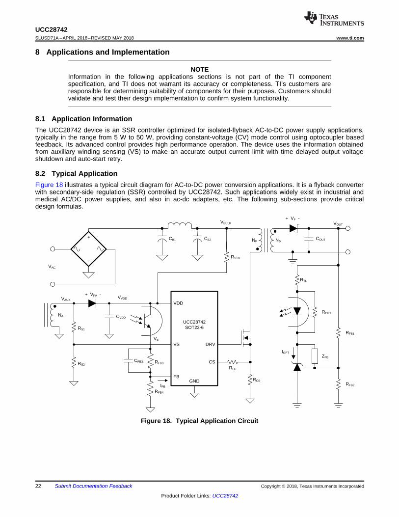
8.2 Typical ApplicationFigure 18 illustrates a typical circuit diagram for AC-to-DC power conversion applications. It is a flyback converterwith secondary-side regulation (SSR) controlled by UCC28742. Such applications widely exist in industrial andmedical AC/DC power supplies, and also in ac-dc adapters, etc. The following sub-sections provide criticaldesign formulas.
Figure 18. Typical Application Circuit
23
UCC28742www.ti.com SLUSD71A –APRIL 2018–REVISED MAY 2018
Product Folder Links: UCC28742
Submit Documentation FeedbackCopyright © 2018, Texas Instruments Incorporated
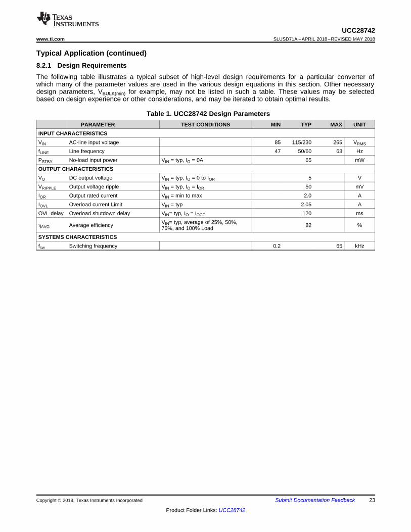
Typical Application (continued)8.2.1 Design RequirementsThe following table illustrates a typical subset of high-level design requirements for a particular converter ofwhich many of the parameter values are used in the various design equations in this section. Other necessarydesign parameters, VBULK(min) for example, may not be listed in such a table. These values may be selectedbased on design experience or other considerations, and may be iterated to obtain optimal results.
Table 1. UCC28742 Design ParametersPARAMETER TEST CONDITIONS MIN TYP MAX UNIT
INPUT CHARACTERISTICSVIN AC-line input voltage 85 115/230 265 VRMS
fLINE Line frequency 47 50/60 63 HzPSTBY No-load input power VIN = typ, IO = 0A 65 mWOUTPUT CHARACTERISTICSVO DC output voltage VIN = typ, IO = 0 to IOR 5 VVRIPPLE Output voltage ripple VIN = typ, IO = IOR 50 mVIOR Output rated current VIN = min to max 2.0 AIOVL Overload current Limit VIN = typ 2.05 AOVL delay Overload shutdown delay VIN= typ, IO = IOCC 120 ms
ηAVG Average efficiency VIN= typ, average of 25%, 50%,75%, and 100% Load 82 %
SYSTEMS CHARACTERISTICSfsw Switching frequency 0.2 65 kHz
IN(min)
STRDD(on) DD
STARTSTR
2 VR
V CI
t
u
u
24
UCC28742SLUSD71A –APRIL 2018–REVISED MAY 2018 www.ti.com
Product Folder Links: UCC28742
Submit Documentation Feedback Copyright © 2018, Texas Instruments Incorporated
8.2.2 Detailed Design ProcedureThis procedure outlines the steps to design a constant output voltage (VOCV) flyback converter using theUCC28742 controller. Please refer to the Figure 18 for circuit details and section for variable definitions used inthe applications equations below.
8.2.2.1 Custom Design With WEBENCH® ToolsClick here to create a custom design using the UCC28742 device with the WEBENCH® Power Designer.1. Start by entering the input voltage (VIN), output voltage (VOUT), and output current (IOUT) requirements.2. Optimize the design for key parameters such as efficiency, footprint, and cost using the optimizer dial.3. Compare the generated design with other possible solutions from Texas Instruments.
The WEBENCH Power Designer provides a customized schematic along with a list of materials with real-timepricing and component availability.
In most cases, these actions are available:• Run electrical simulations to see important waveforms and circuit performance• Run thermal simulations to understand board thermal performance• Export customized schematic and layout into popular CAD formats• Print PDF reports for the design, and share the design with colleagues
Get more information about WEBENCH tools at www.ti.com/WEBENCH.
8.2.2.2 VDD Capacitance, CDD
The capacitance on VDD needs to supply the device operating current until the output of the converter reachesthe target minimum operating voltage. At this time the auxiliary winding can sustain the voltage to theUCC28742. The total output current available to the load and to charge the output capacitors is the constant-current regulation target. The equation below assumes the output current of the flyback is available to charge theoutput capacitance until the minimum output voltage is achieved to maintain VDD above its VVDD(on). The gate-drive current depends on particular MOSFET to be used. If with an estimated average 1.0 mA of gate-drivecurrent, CDD is determined by Equation 6, and at IOCC, VOCC = VOCV.
(6)
8.2.2.3 VDD Start-Up Resistance, RSTR
Once the VDD capacitance is known, the start-up resistance from VBULK to achieve the power-on delay time(tSTR) target can be determined.
(7)
CCR PSCS XFMR
OCC
V NR
2 I
u u K
u
MAX BULK min
PS max
MAGCC OCV F
D V
ND V V
u
u
RMAX MAX MAGCC
tD 1 f D
2§ ·
u ¨ ¸© ¹
BULK(min)IN
IN(min)BULK 2 2
IN(min) BULK(min) LINE
V1P 0.5 arcsin
2 VC
2V V f
§ ·§ ·¨ ¸¨ ¸u u
¨ ¸S¨ ¸u© ¹© ¹ u
OCV OCCIN
V IP
u
K
25
UCC28742www.ti.com SLUSD71A –APRIL 2018–REVISED MAY 2018
Product Folder Links: UCC28742
Submit Documentation FeedbackCopyright © 2018, Texas Instruments Incorporated
8.2.2.4 Input Bulk Capacitance and Minimum Bulk VoltageDetermine the minimum voltage on the input capacitance, CB1 and CB2 total, in order to determine the maximumNp to Ns turns ratio of the transformer. The input power of the converter based on target full-load efficiency,minimum input rms voltage, and minimum AC input frequency are used to determine the input capacitancerequirement.
Maximum input power is determined based on VOCV, load current over load IOVL= IOCC, and the full-load efficiencytarget. An initial estimate of efficiency can be assumed for full-load efficiency, for example 89% for a converter ofrated power 48 W and output voltage 24 V.
(8)
Equation 9 provides an accurate solution for input capacitance based on a target minimum bulk capacitorvoltage. To target a given input capacitance value, iterate the minimum capacitor voltage to achieve the targetcapacitance.
(9)
8.2.2.5 Transformer Turns Ratio, Inductance, Primary-Peak CurrentThe maximum primary-to-secondary turns ratio can be determined by the target maximum switching frequency atfull load, the minimum input capacitor bulk voltage, and the estimated DCM resonant time.
Initially determine the maximum available total duty cycle of the on time and secondary conduction time based ontarget switching frequency and DCM resonant time. For DCM resonant time, assume 500 kHz if you do not havean estimate from previous designs. For the transition mode operation limit, the period required from the end ofsecondary current conduction to the first valley of the VDS voltage is ½ of the DCM resonant period, or 1 µsassuming 500-kHz resonant frequency. DMAX can be determined using Equation 10.
(10)
Once DMAX is known, the maximum turns ratio of the primary to secondary can be determined with the equationbelow. DMAGCC is defined as the secondary diode conduction duty cycle when load current reaches a specifiedlimit operation. It is set internally by the UCC28742 at 0.475. The total voltage on the secondary winding needsto be determined; which is the sum of VOCV and the secondary rectifier VF.
(11)
NPS is determined also with other design factors such as voltage and current ratings of primary MOSFET,secondary rectifier diode, as well as secondary MOSFET if synchronous rectifier is used. Once an optimumturns-ratio is determined from a detailed transformer design, use this ratio for the following parameters.
The UCC28742 controller constant current limit is achieved by maintaining DMAGCC = 0.475 at the maximumprimary current setting. The transformer turns ratio and current limit determine the current sense resistor for atarget constant current limit.
Since not all of the energy stored in the transformer is transferred to the secondary, a transformer efficiency termis included. This efficiency number includes the core and winding losses, leakage inductance ratio, and biaspower ratio to rated output power. A bias power can be initially estimated at 0.1% to 0.5% rated powerdepending on power rating. An overall transformer efficiency of 94.5% is a good estimation of assuming 2%leakage inductance, 3% core and winding loss, and 0.5% bias power.
RCS is used to program the primary-peak current with Equation 12:
(12)
ON(min) IN(max)
DMAG(min)PS OCV F
t V 2t
N V V
u u
u
PP(max)PON(min)
AMIN(max)
ILt
KV 2 u
u
DSPK OCV F PS LKIN maxV V 2 V V N V u u
IN max
REV OCV
PS
V 2
V VN
u
DD(off) FAAS
OCC F
V VN
V V
u u K u u
OCV F OCCP 2
XFMR MAXPP(max)
2 V V IL
I f
CST(max)PP(max)
CS
VI
R
26
UCC28742SLUSD71A –APRIL 2018–REVISED MAY 2018 www.ti.com
Product Folder Links: UCC28742
Submit Documentation Feedback Copyright © 2018, Texas Instruments Incorporated
The primary transformer inductance can be calculated using the standard energy storage equation for flybacktransformers. Primary current, maximum switching frequency, output and transformer efficiency are included inEquation 14.
Initially the transformer primary current should be determined. Primary current is simply the maximum currentsense threshold divided by the current sense resistance.
(13)
(14)
The primary inductance LP in Equation 14 also needs to consider primary MOSFET minimum turn on time asdescribed in Transformer Parameter Verification.
The auxiliary winding to secondary winding transformer turns-ratio (NAS) is determined by the lowest targetoperating output voltage VOVL at current limit and above the VDD(off) of the UCC28742. The output voltagereaches VOVL when output current reaches its limit IOCC; VOVL is determined by IOCC and the expected minimumload resistance RLOAD at IOCC, i.e., VOVL = IOCC x RLOAD. Note that VOVL can only be maintained within typical120ms, and after that time, the output voltage will enter the cycle of shutdown and auto-start retry, as describedin Constant Current Limit and Delayed Shutdown, and shown in Figure 14 and Figure 15. There is additionalenergy supplied to VDD from the transformer leakage inductance energy which may allow a slightly lower turns-ratio to be used in a design. The NAS is then determined by the below equation.
(15)
8.2.2.6 Transformer Parameter VerificationThe transformer turns-ratio selected affects the MOSFET VDS and secondary rectifier reverse voltage so theseshould be reviewed. The UCC28742 controller requires a minimum on time of the MOSFET (tON) and minimumDMAG time (tDMAG(min)) of the secondary rectifier in the high line, under minimum-load condition. The selection offMAX, LP and RCS affects the minimum tON and tDMAG.
The secondary rectifier and MOSFET voltage stress can be determined by the equations below.
(16)
For the MOSFET VDS voltage stress, an estimated leakage inductance voltage spike (VLK) needs to be included.
(17)
The following equations are used to determine for the minimum tON target of 0.35 µs and minimum de-mag time,tDMAG(min), target of 1.7 µs. Notice that the minimum tON target of 0.35 µs is determined by CS pin Leading-edgeblanking time, TCSLEB in Electrical Characteristics. The target is to design LP and make tON(min) ≥TCSLEB . But invery worst normal operation condition, during the tON(min) , the CS pin OCP should not be triggered, i.e., the CSpin should not reach near 1.41 V defined by VOCP in Electrical Characteristics.
(18)
(19)
LC S1 CS D GATE _ OFF PALC
P
K R R (t t ) NR
L
u u u u
u
u
S1 OVPS2
AS OV F OVP
R VR
N (V V ) V
IN(run)
S1PA VSL(run)
V 2R
N I
u
u
27
UCC28742www.ti.com SLUSD71A –APRIL 2018–REVISED MAY 2018
Product Folder Links: UCC28742
Submit Documentation FeedbackCopyright © 2018, Texas Instruments Incorporated
8.2.2.7 VS Resistor Divider and Line CompensationThe VS divider resistors determine the output voltage regulation point of the flyback converter, also the high-sidedivider resistor (RS1) determines the line voltage at which the controller enables continuous DRV operation. RS1is initially determined based on the transformer auxiliary to primary turns-ratio and the desired input voltageoperating threshold.
(20)
IVSL(run) is VS pin run current with a typical value 210 µA for a design. The low-side VS pin resistor is selectedbased on desired output over voltage VOV.
(21)
The UCC28742 can maintain tight output current limit over input line by utilizing the line compensation feature.The line compensation resistor (RLC) value is determined by current flowing in RS1 and expected gate drive andMOSFET turn-off delay. Assume a 50-ns internal delay in the UCC28742.
(22)
RIPPLE RIPPLE_R RIPPLE_CV 0.81 V 1.15 V 10mV u u
_
2
PP max
RIPPLE COCV
LP I 1COUT
V4 V
u u
u
ESR RIPPLE_RPP(max) PS
1R V
I N u
u
TRANSW(min)
OUTO
1I 50 s
fC
V
§ · P¨ ¸¨ ¸
© ¹ '
SB SB _ CONV RSTR SNBRP P P P
2BULK DD
RSTRSTR
(V V )P
R
_ _
2
OCV
PL
SB CONV NL BIAS
VR
P P
OUT MINSB _ CONV 2
AM MAX
P fP
K f
u#Ku u
28
UCC28742SLUSD71A –APRIL 2018–REVISED MAY 2018 www.ti.com
Product Folder Links: UCC28742
Submit Documentation Feedback Copyright © 2018, Texas Instruments Incorporated
8.2.2.8 Standby Power EstimateAssuming no-load standby power is a required design parameter, determine the estimated no-load power basedon target converter maximum switching frequency and output power rating. The following equation estimates thestand-by power of the converter.
(23)
The output preload resistor can be estimated by VOCV and the difference between the converter stand-by powerand the no-load bias power PNL_BIAS (that can be set as zero initially and adjust it later, particularly through thebench test), then the preload resistor value is estimated in Equation 24 :
(24)
A physical resistor component RPLmay not be needed as other components on the secondary-side such asTL431 can already provide enough preload.
The capacitor bulk voltage for the loss estimation is based on the highest voltage for the standby powermeasurement, typically as 325 VDC (or AC input of 230 Vrms). Power loss of RSTR is estimated inEquation 25:
(25)
The total standby power, including the converter standby power loss, the start-up resistance power, and thesnubber power loss, is estimated in Equation 26:
(26)
8.2.2.9 Output CapacitanceThe output capacitance value is typically determined by the transient response requirement. Equation 27assumes that the switching frequency can be at the UCC28742 minimum of fSW(min).
(27)
Another consideration of the output capacitor(s) is the ripple voltage requirement. The output capacitors and theirtotal ESR are the main factors to determine the output voltage ripple. Equation 28 provides a formula todetermine required ESR value RESR, and Equation 28 provides a formula to determine required capacitance. Thetotal output ripple is the sum of these two parts with scale factors and 10mV to consider other noise as shown inEquation 30,
(28)
(29)
(30)
Example: if require VRIPPLE = 70 mV, assume 0.81 × VRIPPLE_R = 1.15 × VRIPPLE_C = 30 mV, then RESR = 4.05mΩ, and COUT = 643 µF, with assumption of LP = 700 µH, IPP(max) = 0.713 A, NPS = 13, VOCV = 5.3 V.
OUTNL OPTNLTL
OPTNL
V V 2 VR
I
CENL OPTNLOPTNL
NL OPT
I VI
CTR R
29
UCC28742www.ti.com SLUSD71A –APRIL 2018–REVISED MAY 2018
Product Folder Links: UCC28742
Submit Documentation FeedbackCopyright © 2018, Texas Instruments Incorporated
8.2.2.10 Feedback Loop Design ConsiderationRefer to Figure 18, the UCC28742 converter feedback network is composed of TL431, optocoupler and severalresistors and capacitors. RFB1 and RFB2 set up the converter output regulation point. A series-resistor RFB3 isnecessary to limit the current into FB and to avoid excess draining of CVDD during this type of transient situation,although connecting the emitter directly to the FB input of the UCC28742 is possible. However, an unload-stepresponse may unavoidably drive the optocoupler into saturation which will overload the FB input with full VDDapplied. The value of RFB3 is to limit the excess IFB to an acceptable level when the optocoupler is saturated. TheRFB3 value is chosen to allow the current into the FB pin to reach the 30 µA. the maximum IFB control level. Thiswill be met if the voltage at IFB can reach 1V at no load conditions. To improve transient response RFB3 can bebypassed with CFB3.
RFB4 can be used to set a nominal operating current of the optocoupler to improve the current transfer ratio andbandwidth of the optocoupler. For low standby power this operating current level should be kept small since itmust be supplied from VDD operating voltage. The value of RFB4 is determined empirically due to the variablenature of the specific optocoupler chosen for the design. The ratio of RFB4 to RFB3 is typically in a range of 1/10 to1/4 with typical value of RFB4 in 4 kΩ to 25 kΩ, and RFB3 in 25 kΩ to 200 kΩ. A good starting point is to selectRFB4 around 4 kΩ and RFB3 around 30 kΩ for a design.
The shunt-regulator compensation network, ZFB, is determined using well-established design techniques forcontrol-loop stability. Typically, a Type-II compensation network is used. An effective approach is to set ZFB to bea capacitor, ZFB = CFB to form an integrator, and adding a bypass capacitor RFB3 will extend the frequencyresponse of the optocoupler CTR.
Referring again to Figure 18, the shunt-regulator (typically a TL431) current is at about 1 mA even when almostno optocoupler diode current flows. Since even a near-zero diode current establishes a forward voltage, ROPT isselected to provide regulator bias current such as for TL431. The optocoupler input diode must be characterizedby the designer to obtain the actual forward voltage versus forward current at the low currents expected. At thefull-load condition of the converter, IFB is around 0.5 µA, ICE may be around (0.4 V / RFB4), and CTR at this levelis about 10%, so the diode current typically falls in the range of 25 µA to 100 µA. Typical opto-diode forwardvoltage at this level is about 0.97 V which is applied across ROPT. If ROPT is set equal to 1 kΩ, this provides 970µA plus the diode current for IOPT.
As output load decreases, the voltage across the shunt-regulator also decreases to increase the current throughthe optocoupler diode. This increases the diode forward voltage across ROPT. CTR at no-load (when ICE ishigher) is generally a few percent higher than CTR at full-load (when ICE is lower). At steady-state no-loadcondition, the shunt-regulator current is maximized and can be estimated by and Equation 31. IOPTNL, plus thesum of the leakage currents of all the components on the output of the converter, constitute the total currentrequired for use in to estimate secondary-side standby loss.
(31)
The shunt-regulator voltage can decrease to a minimum, saturated level of about 2 V. To prevent excessivediode current, a series resistor, RTL, is added to limit IOPT to the maximum value necessary for regulation.Equation 32 provides an estimated initial value for RTL, which may be adjusted for optimal limiting later during theprototype evaluation process.
(32)
Output Power
Effi
cien
cy
10% 20% 30% 40% 50% 60% 70% 80% 90% 100%60%
62.5%
65%
67.5%
70%
72.5%
75%
77.5%
80%
82.5%
85%
D001
115 V RMS230 V RMS
IOUT (A)
VO
UT (
V)
0 0.2 0.4 0.6 0.8 1 1.2 1.4 1.6 1.8 2 2.20
1
2
3
4
5
6
D002
30
UCC28742SLUSD71A –APRIL 2018–REVISED MAY 2018 www.ti.com
Product Folder Links: UCC28742
Submit Documentation Feedback Copyright © 2018, Texas Instruments Incorporated
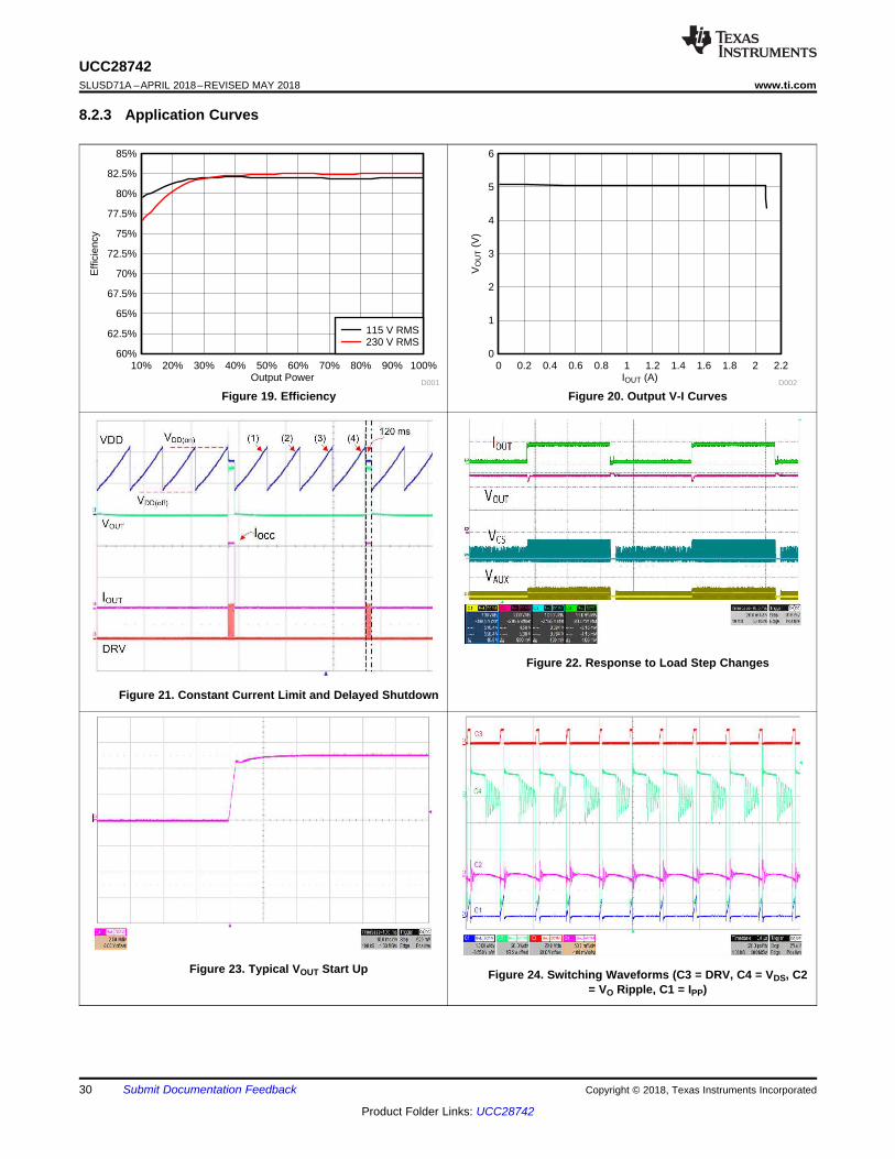
8.2.3 Application Curves
Figure 19. Efficiency Figure 20. Output V-I Curves
Figure 21. Constant Current Limit and Delayed Shutdown
Figure 22. Response to Load Step Changes
Figure 23. Typical VOUT Start Up Figure 24. Switching Waveforms (C3 = DRV, C4 = VDS, C2= VO Ripple, C1 = IPP)
31
UCC28742www.ti.com SLUSD71A –APRIL 2018–REVISED MAY 2018
Product Folder Links: UCC28742
Submit Documentation FeedbackCopyright © 2018, Texas Instruments Incorporated
8.3 Do's and Don'ts• During no-load operation, do allow sufficient margin for variations in VDD level to avoid the UVLO shutdown
threshold. Also, at no-load, keep the average switching frequency greater than 1.5 × fSW(min) typical to avoid arise in output voltage. RLC needs to be adjusted based on no-load operation accounting for both low-line andhigh-line operation..
• Do clean flux residue and contaminants from the PCB after assembly. Uncontrolled leakage current from VSto GND causes the output voltage to increase, while leakage current from VDD to VS can cause outputvoltage to increase.
• If ceramic capacitors are used for VDD, do use quality parts with X7R or X5R dielectric rated 50 V or higherto minimize reduction of capacitance due to DC-bias voltage and temperature variation.
• Do not use leaky components if low stand-by input power consumption is a design requirement.• Do not probe the VS node with an ordinary oscilloscope probe; the probe capacitance can alter the signal and
disrupt regulation.• Do observe VS indirectly by probing the auxiliary winding voltage at RS1 and scaling the waveform by the VS
divider ratio.• Do follow Equation 27 to Equation 30 for COUT.
UCC28742SOT23-6
DRV
CS
VDD
GND
VS
NP NS
NA
VAUX
VAC
FB
+
±
CDD
C01
RCS
RS2
RS1
CB2CB1
RFB4RFB4
CFB
RSN1 CSN1
RSN2
C02 RPL
RG1
RLC
RTL
ROPT
RFB1ZFB
RFB2
IOPT
CY
IsolationBoundary
Optional and shortacross if not usedRSTR
L
N
D2
Kelvin Connection
Optocoupler
+
±
(d) (b)
(c)
(e)(a)
Q1
VOUTVBLK D1
DIN
32
UCC28742SLUSD71A –APRIL 2018–REVISED MAY 2018 www.ti.com
Product Folder Links: UCC28742
Submit Documentation Feedback Copyright © 2018, Texas Instruments Incorporated
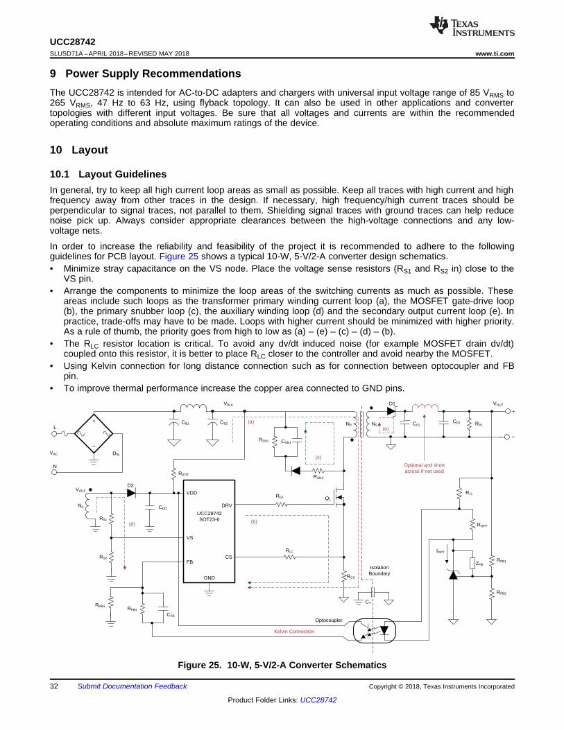
9 Power Supply RecommendationsThe UCC28742 is intended for AC-to-DC adapters and chargers with universal input voltage range of 85 VRMS to265 VRMS, 47 Hz to 63 Hz, using flyback topology. It can also be used in other applications and convertertopologies with different input voltages. Be sure that all voltages and currents are within the recommendedoperating conditions and absolute maximum ratings of the device.
10 Layout
10.1 Layout GuidelinesIn general, try to keep all high current loop areas as small as possible. Keep all traces with high current and highfrequency away from other traces in the design. If necessary, high frequency/high current traces should beperpendicular to signal traces, not parallel to them. Shielding signal traces with ground traces can help reducenoise pick up. Always consider appropriate clearances between the high-voltage connections and any low-voltage nets.
In order to increase the reliability and feasibility of the project it is recommended to adhere to the followingguidelines for PCB layout. Figure 25 shows a typical 10-W, 5-V/2-A converter design schematics.• Minimize stray capacitance on the VS node. Place the voltage sense resistors (RS1 and RS2 in) close to the
VS pin.• Arrange the components to minimize the loop areas of the switching currents as much as possible. These
areas include such loops as the transformer primary winding current loop (a), the MOSFET gate-drive loop(b), the primary snubber loop (c), the auxiliary winding loop (d) and the secondary output current loop (e). Inpractice, trade-offs may have to be made. Loops with higher current should be minimized with higher priority.As a rule of thumb, the priority goes from high to low as (a) – (e) – (c) – (d) – (b).
• The RLC resistor location is critical. To avoid any dv/dt induced noise (for example MOSFET drain dv/dt)coupled onto this resistor, it is better to place RLC closer to the controller and avoid nearby the MOSFET.
• Using Kelvin connection for long distance connection such as for connection between optocoupler and FBpin.
• To improve thermal performance increase the copper area connected to GND pins.
Figure 25. 10-W, 5-V/2-A Converter Schematics
CO1
D1
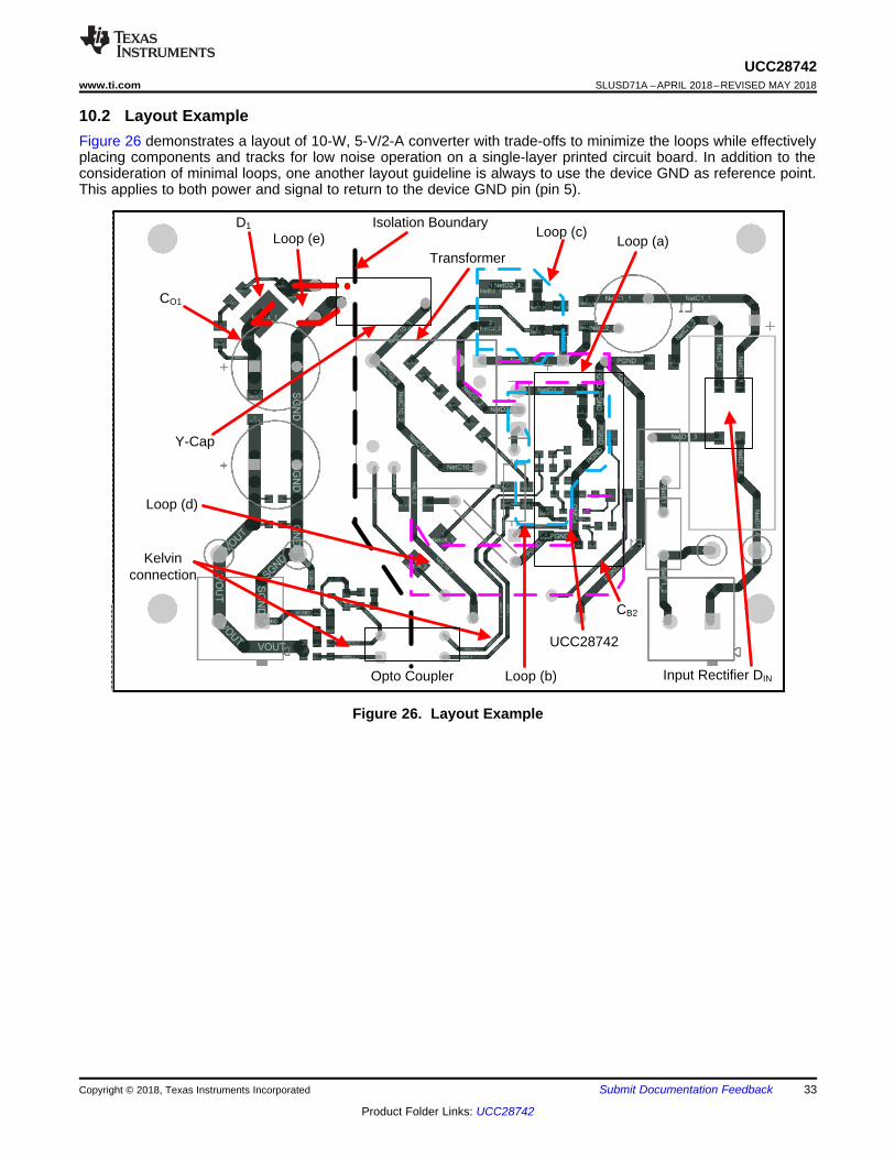
Loop (e)Transformer
Isolation BoundaryLoop (c)
Loop (a)
Input Rectifier DINLoop (b)
UCC28742
CB2
Y-Cap
Loop (d)
Kelvin connection
Opto Coupler
33
UCC28742www.ti.com SLUSD71A –APRIL 2018–REVISED MAY 2018
Product Folder Links: UCC28742
Submit Documentation FeedbackCopyright © 2018, Texas Instruments Incorporated
10.2 Layout ExampleFigure 26 demonstrates a layout of 10-W, 5-V/2-A converter with trade-offs to minimize the loops while effectivelyplacing components and tracks for low noise operation on a single-layer printed circuit board. In addition to theconsideration of minimal loops, one another layout guideline is always to use the device GND as reference point.This applies to both power and signal to return to the device GND pin (pin 5).
Figure 26. Layout Example

34
UCC28742SLUSD71A –APRIL 2018–REVISED MAY 2018 www.ti.com
Product Folder Links: UCC28742
Submit Documentation Feedback Copyright © 2018, Texas Instruments Incorporated
11 Device and Documentation Support
11.1 Device Support
11.1.1 Development Support
11.1.1.1 Custom Design With WEBENCH® ToolsClick here to create a custom design using the UCC28742 device with the WEBENCH® Power Designer.1. Start by entering the input voltage (VIN), output voltage (VOUT), and output current (IOUT) requirements.2. Optimize the design for key parameters such as efficiency, footprint, and cost using the optimizer dial.3. Compare the generated design with other possible solutions from Texas Instruments.
The WEBENCH Power Designer provides a customized schematic along with a list of materials with real-timepricing and component availability.
In most cases, these actions are available:• Run electrical simulations to see important waveforms and circuit performance• Run thermal simulations to understand board thermal performance• Export customized schematic and layout into popular CAD formats• Print PDF reports for the design, and share the design with colleagues
Get more information about WEBENCH tools at www.ti.com/WEBENCH.
11.1.2 Device Nomenclature
11.1.2.1 Capacitance Terms in FaradsCBULK total input capacitance of CB1 and CB2.
CDD minimum required capacitance on the VDD pin.
COUT minimum output capacitance required.
11.1.2.2 Duty Cycle TermsDMAGCC secondary diode conduction duty cycle in CC, 0.475.
DMAX maximum MOSFET on-time duty cycle.
11.1.2.3 Frequency Terms in HertzfLINE minimum line frequency.
fMAX target full-load maximum switching frequency of the converter.
fMIN minimum switching frequency of the converter, add 15% margin over the fSW(min) limit of the device.
fSW(lim) switching frequency in transient after a load step-down change
fSW(min) minimum switching frequency (see the Electrical Characteristics table)
fSW(max) maximum switching frequency (see the Electrical Characteristics table)
fSW(standby) switching frequency before load change at light load condition
11.1.2.4 Current Terms in AmperesIOCC converter output constant-current target.
IOR converter rated output current.
IPP(max) maximum transformer primary current.
ISTART start-up bias supply current (see the Electrical Characteristics table).
ITRAN required positive load-step current.
35
UCC28742www.ti.com SLUSD71A –APRIL 2018–REVISED MAY 2018
Product Folder Links: UCC28742
Submit Documentation FeedbackCopyright © 2018, Texas Instruments Incorporated
Device Support (continued)IVSL(run) VS pin run current (see the Electrical Characteristics table).
IWAIT VDD bias current during the Wait-state . (see the Electrical Characteristics table).
11.1.2.5 Current and Voltage Scaling TermsKAM maximum-to-minimum peak primary current ratio (see the Electrical Characteristics table).
KCo stability factor of 100, used in calculations for COUT.
KLC current-scaling constant (see the Electrical Characteristics table).
36
UCC28742SLUSD71A –APRIL 2018–REVISED MAY 2018 www.ti.com
Product Folder Links: UCC28742
Submit Documentation Feedback Copyright © 2018, Texas Instruments Incorporated
Device Support (continued)11.1.2.6 Transformer TermsLP transformer primary inductance.
LS transformer secondary inductance.
NAS transformer auxiliary-to-secondary turns ratio.
NPA transformer primary-to-auxiliary turns ratio.
NPS transformer primary-to-secondary turns ratio.
NA tnumber of turns of transformer auxiliary winding.
NP tnumber of turns of transformer primary winding.
NS tnumber of turns of transformer secondary winding.
11.1.2.7 Power Terms in WattsPIN converter maximum input power.
POUT full-load output power of the converter.
PRSTR VDD start-up resistor power dissipation.
PSB total stand-by power.
PSB_CONV PSB minus start-up resistor and snubber losses.
11.1.2.8 Resistance Terms in Ω
RCS primary current programming resistance
RESR total ESR of the output capacitor(s).
RPL preload resistance on the output of the converter.
RS1 high-side VS pin resistance.
RS2 low-side VS pin resistance.
RSTR Start-up resistor connected between bulk voltage and VDD
11.1.2.9 Timing Terms in SecondstD current-sense delay.
tDMAG(min) minimum secondary rectifier conduction time.
tGATE_OFF primary-side main MOSFET turn-off time.
tON(min) minimum MOSFET on time.
tR period of the resonant ringing after tDMAG.
tSTR power-on delay time due to charge-up time needed for VDD capacitance CDD.
tZTO tZTO: zero-crossing timeout delay without zero-crossing detected on VS (see the ElectricalCharacteristics table).
37
UCC28742www.ti.com SLUSD71A –APRIL 2018–REVISED MAY 2018
Product Folder Links: UCC28742
Submit Documentation FeedbackCopyright © 2018, Texas Instruments Incorporated
Device Support (continued)11.1.2.10 Voltage Terms in VoltsVBLK or VBULK bulk capacitor voltage.
VBULK(max) highest bulk capacitor voltage for stand-by power measurement.
VBULK(min) minimum voltage on CB1 and CB2 at full power.
VBULK(run) converter start-up (run) bulk voltage.
VCBC cable compensation voltage at the output of board-end at full load.
VCCR constant-current regulating voltage (see the Electrical Characteristics table).
VCCUV VS threshold for constant-current output voltage shutdown (see the Electrical Characteristics table).
VCST(max) CS pin maximum current-sense threshold (see the Electrical Characteristics table).
VCST(min) CS pin minimum current-sense threshold (see the Electrical Characteristics table).
VDD(off) or VVDD(off) UVLO turn-off voltage (see the Electrical Characteristics table).
VVDD(on) or VDD(on) UVLO turn-on voltage (see the Electrical Characteristics table).
VF secondary rectifier forward voltage drop at near-zero current.
VFA auxiliary rectifier forward voltage drop.
VLK estimated leakage inductance energy reset voltage.
VOCV regulated output voltage of the converter.
VOCC target lowest converter output voltage in constant-current regulation.
VOVL The output voltage reaches VOVL when output current reaches its limit IOCC; VOVL is determined byIOCC and the expected minimum load resistance RLOAD at IOCC, i.e., VOVL = IOCC x RLOAD.
VRIPPLE output peak-to-peak ripple voltage at full-load.
VVSR CV regulating level at the VS input (see the Electrical Characteristics table).
11.1.2.11 AC Voltage Terms in VRMS
VIN(max) maximum input voltage to the converter.
VIN(min) minimum input voltage to the converter.
VIN(run) converter input start-up (run) voltage.
11.1.2.12 Efficiency Termsη converter overall efficiency.
η10 efficiency at 10% load.
ηAVG arithmetic average of efficiency at load level 25%, 50%, 75%, and 100% .
ηXFMR transformer primary-to-secondary power transfer efficiency.
11.2 Documentation Support
11.2.1 Related DocumentationFor related documentation see the following:• Using the UCC28742-1EVM-724, Evaluation Module, SLUUBF1• UCC28742 Design CalculatorSLUC652
38
UCC28742SLUSD71A –APRIL 2018–REVISED MAY 2018 www.ti.com
Product Folder Links: UCC28742
Submit Documentation Feedback Copyright © 2018, Texas Instruments Incorporated
11.3 Receiving Notification of Documentation UpdatesTo receive notification of documentation updates, navigate to the device product folder on ti.com. In the upperright corner, click on Alert me to register and receive a weekly digest of any product information that haschanged. For change details, review the revision history included in any revised document.
11.4 Community ResourcesThe following links connect to TI community resources. Linked contents are provided "AS IS" by the respectivecontributors. They do not constitute TI specifications and do not necessarily reflect TI's views; see TI's Terms ofUse.
TI E2E™ Online Community TI's Engineer-to-Engineer (E2E) Community. Created to foster collaborationamong engineers. At e2e.ti.com, you can ask questions, share knowledge, explore ideas and helpsolve problems with fellow engineers.
Design Support TI's Design Support Quickly find helpful E2E forums along with design support tools andcontact information for technical support.
11.5 TrademarksE2E is a trademark of Texas Instruments.WEBENCH is a registered trademark of Texas Instruments.
11.6 Electrostatic Discharge CautionThis integrated circuit can be damaged by ESD. Texas Instruments recommends that all integrated circuits be handled withappropriate precautions. Failure to observe proper handling and installation procedures can cause damage.
ESD damage can range from subtle performance degradation to complete device failure. Precision integrated circuits may be moresusceptible to damage because very small parametric changes could cause the device not to meet its published specifications.
11.7 GlossarySLYZ022 — TI Glossary.
This glossary lists and explains terms, acronyms, and definitions.
12 Mechanical, Packaging, and Orderable InformationThe following pages include mechanical, packaging, and orderable information. This information is the mostcurrent data available for the designated devices. This data is subject to change without notice and revision ofthis document. For browser-based versions of this data sheet, refer to the left-hand navigation.
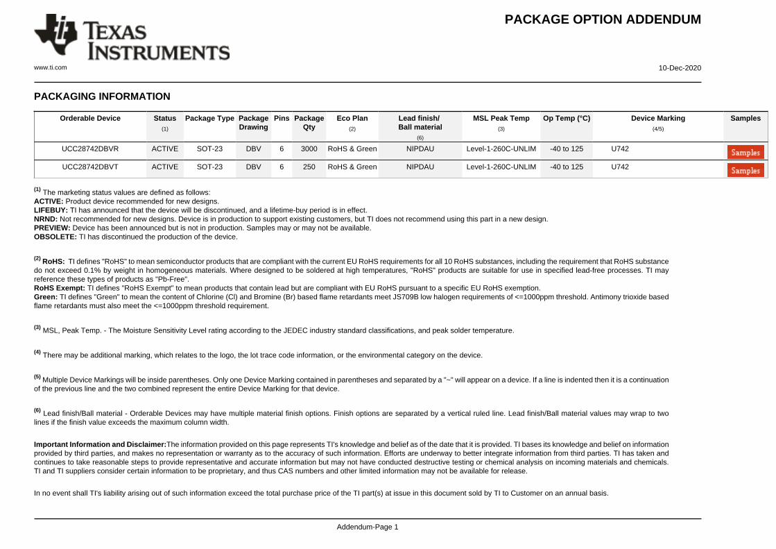
PACKAGE OPTION ADDENDUM
www.ti.com 10-Dec-2020
Addendum-Page 1
PACKAGING INFORMATION
Orderable Device Status(1)
Package Type PackageDrawing
Pins PackageQty
Eco Plan(2)
Lead finish/Ball material
(6)
MSL Peak Temp(3)
Op Temp (°C) Device Marking(4/5)
Samples
UCC28742DBVR ACTIVE SOT-23 DBV 6 3000 RoHS & Green NIPDAU Level-1-260C-UNLIM -40 to 125 U742
UCC28742DBVT ACTIVE SOT-23 DBV 6 250 RoHS & Green NIPDAU Level-1-260C-UNLIM -40 to 125 U742
(1) The marketing status values are defined as follows:ACTIVE: Product device recommended for new designs.LIFEBUY: TI has announced that the device will be discontinued, and a lifetime-buy period is in effect.NRND: Not recommended for new designs. Device is in production to support existing customers, but TI does not recommend using this part in a new design.PREVIEW: Device has been announced but is not in production. Samples may or may not be available.OBSOLETE: TI has discontinued the production of the device.
(2) RoHS: TI defines "RoHS" to mean semiconductor products that are compliant with the current EU RoHS requirements for all 10 RoHS substances, including the requirement that RoHS substancedo not exceed 0.1% by weight in homogeneous materials. Where designed to be soldered at high temperatures, "RoHS" products are suitable for use in specified lead-free processes. TI mayreference these types of products as "Pb-Free".RoHS Exempt: TI defines "RoHS Exempt" to mean products that contain lead but are compliant with EU RoHS pursuant to a specific EU RoHS exemption.Green: TI defines "Green" to mean the content of Chlorine (Cl) and Bromine (Br) based flame retardants meet JS709B low halogen requirements of <=1000ppm threshold. Antimony trioxide basedflame retardants must also meet the <=1000ppm threshold requirement.
(3) MSL, Peak Temp. - The Moisture Sensitivity Level rating according to the JEDEC industry standard classifications, and peak solder temperature.
(4) There may be additional marking, which relates to the logo, the lot trace code information, or the environmental category on the device.
(5) Multiple Device Markings will be inside parentheses. Only one Device Marking contained in parentheses and separated by a "~" will appear on a device. If a line is indented then it is a continuationof the previous line and the two combined represent the entire Device Marking for that device.
(6) Lead finish/Ball material - Orderable Devices may have multiple material finish options. Finish options are separated by a vertical ruled line. Lead finish/Ball material values may wrap to twolines if the finish value exceeds the maximum column width.
Important Information and Disclaimer:The information provided on this page represents TI's knowledge and belief as of the date that it is provided. TI bases its knowledge and belief on informationprovided by third parties, and makes no representation or warranty as to the accuracy of such information. Efforts are underway to better integrate information from third parties. TI has taken andcontinues to take reasonable steps to provide representative and accurate information but may not have conducted destructive testing or chemical analysis on incoming materials and chemicals.TI and TI suppliers consider certain information to be proprietary, and thus CAS numbers and other limited information may not be available for release.
In no event shall TI's liability arising out of such information exceed the total purchase price of the TI part(s) at issue in this document sold by TI to Customer on an annual basis.
PACKAGE OPTION ADDENDUM
www.ti.com 10-Dec-2020
Addendum-Page 2
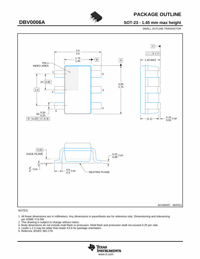
www.ti.com
PACKAGE OUTLINE
C
0.220.08 TYP
0.25
3.02.6
2X 0.95
1.45 MAX
0.150.00 TYP
6X 0.500.25
0.60.3 TYP
80 TYP
1.9
A
3.052.75
B1.751.45
(1.1)
SOT-23 - 1.45 mm max heightDBV0006ASMALL OUTLINE TRANSISTOR
4214840/C 06/2021
NOTES: 1. All linear dimensions are in millimeters. Any dimensions in parenthesis are for reference only. Dimensioning and tolerancing per ASME Y14.5M.2. This drawing is subject to change without notice.3. Body dimensions do not include mold flash or protrusion. Mold flash and protrusion shall not exceed 0.25 per side.4. Leads 1,2,3 may be wider than leads 4,5,6 for package orientation.5. Refernce JEDEC MO-178.
0.2 C A B
1
34
52
INDEX AREAPIN 1
6
GAGE PLANE
SEATING PLANE
0.1 C
SCALE 4.000
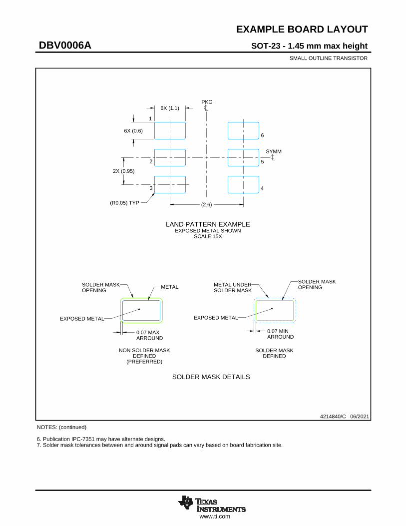
www.ti.com
EXAMPLE BOARD LAYOUT
0.07 MAXARROUND
0.07 MINARROUND
6X (1.1)
6X (0.6)
(2.6)
2X (0.95)
(R0.05) TYP
4214840/C 06/2021
SOT-23 - 1.45 mm max heightDBV0006ASMALL OUTLINE TRANSISTOR
NOTES: (continued) 6. Publication IPC-7351 may have alternate designs. 7. Solder mask tolerances between and around signal pads can vary based on board fabrication site.
SYMM
LAND PATTERN EXAMPLEEXPOSED METAL SHOWN
SCALE:15X
PKG
1
3 4
52
6
SOLDER MASKOPENINGMETAL UNDER
SOLDER MASK
SOLDER MASKDEFINED
EXPOSED METAL
METALSOLDER MASKOPENING
NON SOLDER MASKDEFINED
(PREFERRED)
SOLDER MASK DETAILS
EXPOSED METAL
www.ti.com
EXAMPLE STENCIL DESIGN
(2.6)
2X(0.95)
6X (1.1)
6X (0.6)
(R0.05) TYP
SOT-23 - 1.45 mm max heightDBV0006ASMALL OUTLINE TRANSISTOR
4214840/C 06/2021
NOTES: (continued) 8. Laser cutting apertures with trapezoidal walls and rounded corners may offer better paste release. IPC-7525 may have alternate design recommendations. 9. Board assembly site may have different recommendations for stencil design.
SOLDER PASTE EXAMPLEBASED ON 0.125 mm THICK STENCIL
SCALE:15X
SYMM
PKG
1
3 4
52
6

IMPORTANT NOTICE AND DISCLAIMERTI PROVIDES TECHNICAL AND RELIABILITY DATA (INCLUDING DATASHEETS), DESIGN RESOURCES (INCLUDING REFERENCEDESIGNS), APPLICATION OR OTHER DESIGN ADVICE, WEB TOOLS, SAFETY INFORMATION, AND OTHER RESOURCES “AS IS”AND WITH ALL FAULTS, AND DISCLAIMS ALL WARRANTIES, EXPRESS AND IMPLIED, INCLUDING WITHOUT LIMITATION ANYIMPLIED WARRANTIES OF MERCHANTABILITY, FITNESS FOR A PARTICULAR PURPOSE OR NON-INFRINGEMENT OF THIRDPARTY INTELLECTUAL PROPERTY RIGHTS.These resources are intended for skilled developers designing with TI products. You are solely responsible for (1) selecting the appropriateTI products for your application, (2) designing, validating and testing your application, and (3) ensuring your application meets applicablestandards, and any other safety, security, or other requirements. These resources are subject to change without notice. TI grants youpermission to use these resources only for development of an application that uses the TI products described in the resource. Otherreproduction and display of these resources is prohibited. No license is granted to any other TI intellectual property right or to any third partyintellectual property right. TI disclaims responsibility for, and you will fully indemnify TI and its representatives against, any claims, damages,costs, losses, and liabilities arising out of your use of these resources.TI’s products are provided subject to TI’s Terms of Sale (https:www.ti.com/legal/termsofsale.html) or other applicable terms available eitheron ti.com or provided in conjunction with such TI products. TI’s provision of these resources does not expand or otherwise alter TI’sapplicable warranties or warranty disclaimers for TI products.IMPORTANT NOTICE
Mailing Address: Texas Instruments, Post Office Box 655303, Dallas, Texas 75265Copyright © 2021, Texas Instruments Incorporated
Copyright © 2022 FDOKUMEN