
edgar allan poe and female victimization - OhioLINK ETD Center
Upload
khangminh22Category
view
2download
0
TPS23758 IEEE 802.3at PoE PD with No-Opto Sync Flyback DC-DC Controller
1 Features• Complete IEEE 802.3at PD solution for type 1 PoE
– Ethernet Alliance (EA) logo certified designsavailable
– Robust 100-V, 0.36-Ω (typ) hotswap MOSFET• Integrated PWM controller with 0.77-Ω (typ) 150-V
power MOSFET– Flyback controller with PSR
• Supports CCM operation with secondaryside synchronous FET— multi-outputs
• ±1% (typ, 5-V Output) Load regulation(0-100% load range) — with Sync FET
– Supports low-side switch buck topology– Adjustable switching frequency with
synchronization– Soft-start control with advanced startup– Programmable slew rate and frequency
dithering for enhanced EMI reduction• Primary adapter priority input• –40°C to 125°C Junction temperature range• Small 6-mm x 4-mm VSON package
2 Applications• IEEE 802.3at compliant powered devices• VoIP phones• Security cameras• IP phones• Access points
3 DescriptionThe TPS23758 device combines a Power overEthernet (PoE) powered device (PD) interface, a 150-V switching power FET, and a current-mode DC-DCcontroller optimized for flyback topology. The highlevel of integration along with primary side regulation(PSR), spread spectrum frequency dithering (SSFD),and advanced startup makes the TPS23758 an idealsolution for size-constrained applications. The PoEimplementation supports the IEEE 802.3at standardas a 13-W, Type 1 PD.
The PSR feature of the DC-DC controller usesfeedback from an auxiliary winding for control of theoutput voltage, eliminating the need for external shuntregulator and optocoupler. It is optimized for operationin continuous conduction mode (CCM) with secondaryside synchronous rectification, resulting in optimumoverall efficiency, regulation accuracy and step loadresponse over multiple outputs (for example 5-V and3.3-V output). Typically, the converter operates at aswitching frequency of 250 kHz.
SFFD and slew rate control helps to minimize the sizeand cost of the EMI filter. Advanced Startup allows theuse of minimal bias capacitor while simplifyingconverter startup and hiccup design.
Primary auxiliary power detect (APD) pin can be usedto provide priority for a primary side power adapter.
The DC-DC controller features adjustable soft-start,slope compensation, and blanking. For non-isolatedapplications, the buck topology is also supported bythe TPS23758.
Device Information (1)
PART NUMBER PACKAGE BODY SIZE (NOM)TPS23758 VSON (24) 6.00 mm × 4.00 mm
(1) For all available packages, see the orderable addendum atthe end of the data sheet.
Simplified ApplicationLoad Current (A)
Eff
icie
ncy (
%)
0 0.25 0.5 0.75 1 1.25 1.5 1.75 2 2.250
10
20
30
40
50
60
70
80
90
100
D026
PoEDC-DC
Efficiency Vs. Load Current, Output
www.ti.comTPS23758
SLVSDW3A – APRIL 2019 – REVISED NOVEMBER 2020
Copyright © 2020 Texas Instruments Incorporated Submit Document Feedback 1
Product Folder Links: TPS23758
TPS23758SLVSDW3A – APRIL 2019 – REVISED NOVEMBER 2020
An IMPORTANT NOTICE at the end of this data sheet addresses availability, warranty, changes, use in safety-critical applications,intellectual property matters and other important disclaimers. PRODUCTION DATA.

Table of Contents1 Features............................................................................12 Applications..................................................................... 13 Description.......................................................................14 Revision History.............................................................. 25 Pin Configuration and Functions...................................36 Specifications.................................................................. 5
6.1 Absolute Maximum Ratings........................................ 56.2 ESD Ratings............................................................... 56.3 Recommended Operating Conditions.........................66.4 Thermal Information....................................................66.5 Electrical Characteristics: DC-DC Controller
Section.......................................................................... 76.6 Electrical Characteristics: PoE and Control................ 96.7 Typical Characteristics.............................................. 10
7 Detailed Description......................................................147.1 Overview................................................................... 147.2 Functional Block Diagram......................................... 157.3 Feature Description...................................................16
7.4 Device Functional Modes..........................................218 Application and Implementation.................................. 30
8.1 Application Information............................................. 308.2 Typical Application.................................................... 30
9 Power Supply Recommendations................................3710 Layout...........................................................................37
10.1 Layout Guidelines................................................... 3710.2 Layout Example...................................................... 37
11 Device and Documentation Support..........................3911.1 Related documentation........................................... 3911.2 Support Resources................................................. 3911.3 Trademarks............................................................. 3911.4 Electrostatic Discharge Caution.............................. 3911.5 Glossary.................................................................. 39
12 Mechanical, Packaging, and OrderableInformation.................................................................... 3912.1 Package Option Addendum....................................40
4 Revision HistoryChanges from Revision * (April 2019) to Revision A (November 2020) Page• Updated the numbering format for tables, figures and cross-references throughout the document...................1• Updated Simplified Application with Dvb............................................................................................................ 1• Added, "...and 6.2-V Zener diode..."................................................................................................................... 3• Added paragraph, "VB is the 5-V bias rail...".................................................................................................... 17• Updated Figure 8-1 to include Dvb................................................................................................................... 30• Added section, "Bias Voltage, CVB and DVB"..................................................................................................31
TPS23758SLVSDW3A – APRIL 2019 – REVISED NOVEMBER 2020 www.ti.com
2 Submit Document Feedback Copyright © 2020 Texas Instruments Incorporated
Product Folder Links: TPS23758

5 Pin Configuration and Functions
CP
GND
NC
24
23
21
SRF
VCCSRR
DRAINRSNS
20 TST
19
18
17
16
15
14
13
APD
CS
FRS
DTHR
VB
VSS
RTN
FB
CLS
SST
COMP
DEN
VPD
VDD
A1
A2 A3
A4
2
3
4
5
6
7
8
9
10
11
12
1
Figure 5-1. Package Pinout
Table 5-1. Pin FunctionsPIN
I/O DESCRIPTIONNO. NAME1 RSNS O Switching Power FET source connection. Connect to the external power current sense resistor.
2 CP O CP provides the clamp for the primary side regulation loop. Connect this pin to the lower end of thesecond primary side winding of the transformer.
3 GND — Power ground used by the flyback power FET gate driver and CP. Connect to RTN.
4 SRR I Switching FET Gate sinking current input, used for EMI control. Connect a resistance from SRR toGND to control the Vds rate of rise.
5 SRF I Switching FET Gate sourcing current input, used for EMI control. Connect a resistance from SRFto VB to control the Vds rate of fall.
6 VB O 5-V bias rail for the switching FET gate driver circuit. For internal use only. Bypass with a 0.1-μFceramic capacitor and 6.2-V Zener diode to GND pin.
7 APD I Primary auxiliary power detect input. Raise 1.5 V above RTN to disable pass MOSFET. If not used,connect APD to RTN.
8 CS I DC-DC controller current sense input. Connect directly to the external power current sense resistor.
9 DTHR O Used for spread spectrum frequency dithering. Connect a capacitor from DTHR to RTN and aresistor from DTHR to FRS. If dithering is not used, short DTHR to VB pin.
10 FRS I/O This pin controls the switching frequency of the DC-DC converter. Tie a resistor from this pin toRTN to set the frequency.
11 RTN — RTN is the output of the PoE hotswap and the reference ground for the DC-DC controller.
12 VSS — Negative power rail derived from the PoE source.
13 VDD — Source of DC-DC converter start-up current. For flyback applications, connect to VPD through adiode and bypass with a 0.22 µF to RTN. For buck applications, connect directly to VPD.
14 VPD — Positive input power rail for PoE interface circuit. Derived from the PoE source. Bypass with a 0.1µF to VSS and protect with a TVS.
15 DEN I/O Connect a 24.9-kΩ resistor from DEN to VPD to provide the PoE detection signature. Pulling thispin to VSS during powered operation causes the internal hotswap MOSFET to turn off.
16 CLS O Connect a resistor from CLS to VSS to program the classification current.
17 SST I SST sets the soft-start and the hiccup timer for the DC-DC converter. Connect a capacitor from thispin to RTN to set the DC/DC startup rate.
www.ti.comTPS23758
SLVSDW3A – APRIL 2019 – REVISED NOVEMBER 2020
Copyright © 2020 Texas Instruments Incorporated Submit Document Feedback 3
Product Folder Links: TPS23758
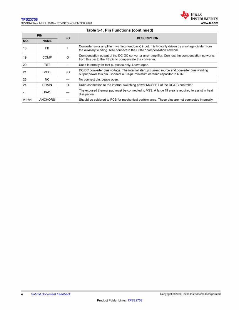
Table 5-1. Pin Functions (continued)PIN
I/O DESCRIPTIONNO. NAME
18 FB I Converter error amplifier inverting (feedback) input. It is typically driven by a voltage divider fromthe auxiliary winding. Also connect to the COMP compensation network.
19 COMP O Compensation output of the DC-DC convertor error amplifier. Connect the compensation networksfrom this pin to the FB pin to compensate the converter.
20 TST — Used internally for test purposes only. Leave open.
21 VCC I/O DC/DC converter bias voltage. The internal startup current source and converter bias windingoutput power this pin. Connect a 3.3-µF minimum ceramic capacitor to RTN.
23 NC — No connect pin. Leave open.
24 DRAIN O Drain connection to the internal switching power MOSFET of the DC/DC controller.
- PAD — The exposed thermal pad must be connected to VSS. A large fill area is required to assist in heatdissipation.
A1-A4 ANCHORS — Should be soldered to PCB for mechanical performance. These pins are not connected internally.
TPS23758SLVSDW3A – APRIL 2019 – REVISED NOVEMBER 2020 www.ti.com
4 Submit Document Feedback Copyright © 2020 Texas Instruments Incorporated
Product Folder Links: TPS23758
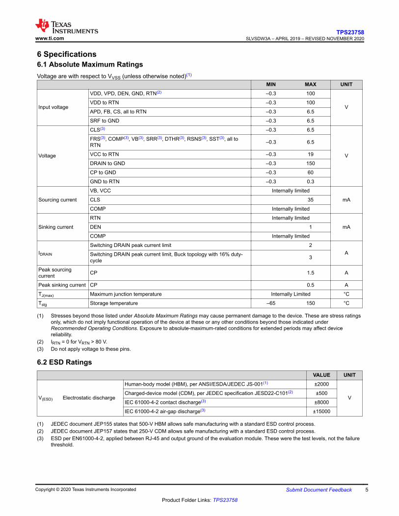
6 Specifications6.1 Absolute Maximum RatingsVoltage are with respect to VVSS (unless otherwise noted)(1)
MIN MAX UNIT
Input voltage
VDD, VPD, DEN, GND, RTN(2) –0.3 100
VVDD to RTN –0.3 100
APD, FB, CS, all to RTN –0.3 6.5
SRF to GND –0.3 6.5
Voltage
CLS(3) –0.3 6.5
V
FRS(3), COMP(3), VB(3), SRR(3), DTHR(3), RSNS(3), SST(3), all toRTN –0.3 6.5
VCC to RTN –0.3 19
DRAIN to GND –0.3 150
CP to GND –0.3 60
GND to RTN –0.3 0.3
Sourcing current
VB, VCC Internally limited
mACLS 35
COMP Internally limited
Sinking current
RTN Internally limited
mADEN 1
COMP Internally limited
IDRAIN
Switching DRAIN peak current limit 2ASwitching DRAIN peak current limit, Buck topology with 16% duty-
cycle 3
Peak sourcingcurrent CP 1.5 A
Peak sinking current CP 0.5 A
TJ(max) Maximum junction temperature Internally Limited °C
Tstg Storage temperature –65 150 °C
(1) Stresses beyond those listed under Absolute Maximum Ratings may cause permanent damage to the device. These are stress ratingsonly, which do not imply functional operation of the device at these or any other conditions beyond those indicated underRecommended Operating Conditions. Exposure to absolute-maximum-rated conditions for extended periods may affect devicereliability.
(2) IRTN = 0 for VRTN > 80 V.(3) Do not apply voltage to these pins.
6.2 ESD RatingsVALUE UNIT
V(ESD) Electrostatic discharge
Human-body model (HBM), per ANSI/ESDA/JEDEC JS-001(1) ±2000
VCharged-device model (CDM), per JEDEC specification JESD22-C101(2) ±500
IEC 61000-4-2 contact discharge(3) ±8000
IEC 61000-4-2 air-gap discharge(3) ±15000
(1) JEDEC document JEP155 states that 500-V HBM allows safe manufacturing with a standard ESD control process.(2) JEDEC document JEP157 states that 250-V CDM allows safe manufacturing with a standard ESD control process.(3) ESD per EN61000-4-2, applied between RJ-45 and output ground of the evaluation module. These were the test levels, not the failure
threshold.
www.ti.comTPS23758
SLVSDW3A – APRIL 2019 – REVISED NOVEMBER 2020
Copyright © 2020 Texas Instruments Incorporated Submit Document Feedback 5
Product Folder Links: TPS23758

6.3 Recommended Operating ConditionsVoltage with respect to VVSS (unless otherwise noted)
MIN NOM MAX UNIT
Input voltage range
VDD, VPD, RTN, GND 0 57
V
VCC to RTN 0 16
APD to RTN 0 VB
CS to RTN 0 2
DRAIN to GND 0 125
CP to GND 0 45
Sinking current RTN 350 mA
Peak current limitDRAIN, RSNS 1.6
ADRAIN, RSNS, Buck topology with 16% duty-cycle 2.5
Peak sourcingcurrent CP 500 mA
Peak sinkingcurrent CP 100 mA
CapacitanceVB(1) 0.08 0.1
μFVCC 0.8 1
Resistance
CLS(1) 30
ΩSRF to VB 100
SRR to GND 15
Synchronizationpulse width input(when used)
FRS 35 ns
TJ Operating junction temperature –40 125 °C
(1) Voltage should not be externally applied to this pin.
6.4 Thermal Information
THERMAL METRIC(1)
TPS23758UNITRJJ (VSON)
24 PINSRθJA Junction-to-ambient thermal resistance 34.7 °C/W
RθJC(top) Junction-to-case (top) thermal resistance 24.5 °C/W
RθJB Junction-to-board thermal resistance 14.5 °C/W
ψJT Junction-to-top characterization parameter 6.4 °C/W
ψJB Junction-to-board characterization parameter 14.5 °C/W
RθJC(bot) Junction-to-case (bottom) thermal resistance 6.4 °C/W
(1) For more information about traditional and new thermal metrics, see the Semiconductor and IC Package Thermal Metrics applicationreport, SPRA953.
TPS23758SLVSDW3A – APRIL 2019 – REVISED NOVEMBER 2020 www.ti.com
6 Submit Document Feedback Copyright © 2020 Texas Instruments Incorporated
Product Folder Links: TPS23758

6.5 Electrical Characteristics: DC-DC Controller SectionUnless otherwise noted, VVDD = 48 V; RDEN = 24.9 kΩ; RFRS = 60.4 kΩ; CLS, RSNS and DRAIN open; CS, APD, and GNDconnected to RTN; SRR connected to GND; SRF, FB and DTHR connected to VB; CVB = 0.1 μF; CCC = 1 μF; CSST = 0.022µF; 8.5 V ≤ VVCC ≤ 16 V; –40°C ≤ TJ ≤ 125°C. Positive currents are into pins unless otherwise noted. Typical values are at25°C.[VVSS = VRTN and VVPD = VVDD] or [VVSS = VRTN = VVPD], all voltages referred to VRTN and VGND unless otherwise noted.
PARAMETER TEST CONDITIONS MIN TYP MAX UNITDC-DC SUPPLY (VCC)VCUVR
Undervoltage lockout
VVCC rising 8 8.25 8.6 V
VCUVF VVCC falling 5.85 6.1 6.25 V
VCUVH Hysteresis(1) 2 2.15 2.5 V
IRUNOperating current, converterswitching
VVCC = 10 V, VFB = VRTN = VRSNS ,DRAIN with 2-kΩ pull up to 95 V, CPwith 2-kΩ pull up to 30 V
2.35 2.7 mA
tST Start-up time, CCC = 1 μFVDD = 10.2 V, VVCC(0) = 0 V 0.5 1.0 2.5 ms
VDD = 35 V, VVCC(0) = 0 V 0.5 0.80 1.5 ms
VVC_ST VCC startup voltage Measure VVCC during startup, IVCC =0 mA 11 13 15.5 V
DC-DC TIMING (FRS)
fSW Switching frequency VFB = VRSNS = VRTN, Measure atDRAIN 223 248 273 kHz
DMAX Duty cycle VFB = VRSNS = VRTN, Measure atDRAIN 75% 77.5% 80%
VSYNC Synchronization Input threshold 2 2.2 2.4 V
FREQUENCY DITHERING RAMP GENERATOR (DTHR)
IDTRCH Charging (sourcing) current 0.5 V < VDTHR < 1.38 V3 x IFRS µA
47.2 49.6 52.1 µA
IDTRDC Discharging (sinking) current 0.6 V < VDTHR < 1.5 V3 x IFRS µA
47.2 49.6 52.1 µA
VDTUT Dithering upper threshold VDTHR rising until IDTHR > 0 1.41 1.513 1.60 V
VDTLT Dithering lower threshold VDTHR falling until IDTHR < 0 0.43 0.487 0.54 V
VDTPP Dithering pk-pk amplitude 1.005 1.026 1.046 V
ERROR AMPLIFIER (FB, COMP)VREFC Feedback regulation voltage 1.723 1.75 1.777 V
IFB_LK FB leakage current (source or sink) VFB-RTN = 1.75 V 0.5 μA
GBW Small signal unity gain bandwidth 0.9 1.2 MHz
AOL Open loop voltage gain 70 90 dB
VZDC 0% duty-cycle threshold VCOMP falling until DRAIN switchingstops 1.35 1.5 1.65 V
ICOMPH COMP source current VFB = VRTN , VCOMP = 3 V 1 mA
ICOMPL COMP sink current VFB = VVB , VCOMP = 1.25 V 2.1 6 mA
VCOMPH COMP high voltage VFB = VVB , 15 kΩ from COMP toRTN 4 5 V
VCOMPL COMP low voltage VFB = VVB , 15 kΩ from COMP to VB 1.1 V
COMP to CS gain ΔVCS / ΔVCOMP , 0 V < VCS < 0.5 V 0.475 0.5 0.525 V/V
SOFT-START (SST)
ISSC Charge (sourcing) current SST charging, VSST between lowerand higher threshold 3 4 5 µA
ISSD Discharge (sinking) current SST discharging, VSST betweenlower and higher threshold 3 4 5 µA
www.ti.comTPS23758
SLVSDW3A – APRIL 2019 – REVISED NOVEMBER 2020
Copyright © 2020 Texas Instruments Incorporated Submit Document Feedback 7
Product Folder Links: TPS23758

6.5 Electrical Characteristics: DC-DC Controller Section (continued)Unless otherwise noted, VVDD = 48 V; RDEN = 24.9 kΩ; RFRS = 60.4 kΩ; CLS, RSNS and DRAIN open; CS, APD, and GNDconnected to RTN; SRR connected to GND; SRF, FB and DTHR connected to VB; CVB = 0.1 μF; CCC = 1 μF; CSST = 0.022µF; 8.5 V ≤ VVCC ≤ 16 V; –40°C ≤ TJ ≤ 125°C. Positive currents are into pins unless otherwise noted. Typical values are at25°C.[VVSS = VRTN and VVPD = VVDD] or [VVSS = VRTN = VVPD], all voltages referred to VRTN and VGND unless otherwise noted.
PARAMETER TEST CONDITIONS MIN TYP MAX UNITVSFST Soft-start lower threshold 0.15 0.2 0.25 V
VSTUOF Startup turn off threshold VSST rising until VCC startup turnsoff 1.99 2.1 2.21 V
VSSOFS Soft-start offset voltage VSST rising until start of switching 0.2 0.25 0.3 V
VSSCL Soft-start clamp 2.3 2.6 V
CURRENT SENSE (CS)VCSMAX Maximum threshold voltage VFB = VRTN, VCS rising 0.5 0.55 0.6 V
tOFFDEL_ILM Current limit turnoff delay VCS = 0.65 V 25 41 60ns
tOFFDEL_PW PWM comparator turnoff delay VCS = 0.4 V 25 41 60
Blanking delay In addtition to tOFFDEL 56.5 75 93.5 ns
VSLOPE Internal slope compensation voltage Peak voltage at maximum dutycycle, referred to CS 120 155 185 mV
ISL_EX Peak slope compensation current VFB = VRTN, ICS at maximum dutycycle (ac component) 30 42 54 μA
Bias current DC component of CS current -6.7 -5 -3.3 μA
SWITCHING POWER FET (DRAIN, RSNS)BVDSS Power FET break-down voltage 150 V
RDS(ON) Power FET on resistance 0.77 1.28 Ω
VSDSource-to-drain diode forwardvoltage IRSNS = 500 mA 0.6 1 1.1 V
AUXILIARY POWER DETECTION (APD)VAPDEN APD threshold voltage
VAPD rising 1.42 1.5 1.58 V
VAPDH Hysteresis(1) 0.28 0.3 0.32 V
Leakage current VAPD-RTN = 5 V 1 µA
THERMAL SHUTDOWNTurnoff temperature 145 159 165 °C
Hysteresis(2) 13 °C
(1) The hysteresis tolerance tracks the rising threshold for a given device.(2) These parameters are provided for reference only, and do not constitute part of TI's published device specifications for purposes of TI's
product warranty.
TPS23758SLVSDW3A – APRIL 2019 – REVISED NOVEMBER 2020 www.ti.com
8 Submit Document Feedback Copyright © 2020 Texas Instruments Incorporated
Product Folder Links: TPS23758

6.6 Electrical Characteristics: PoE and ControlUnless otherwise noted, VVPD = 48 V; RDEN = 24.9 kΩ; RFRS = 60.4 kΩ; CLS, RSNS and DRAIN open; CS, APD, and GNDconnected to RTN; SRR connected to GND; SRF, FB and DTHR connected to VB; CVB = 0.1 μF; CCC = 1 μF; CSST = 0.022μF; –40°C ≤ TJ ≤ 125°C. Positive currents are into pins unless otherwise noted. Typical values are at 25°C.Unless otherwise noted, VVPD = VVDD , VVCC = VRTN. All voltages referred to VVSS unless otherwise noted.
PARAMETER TEST CONDITIONS MIN TYP MAX UNIT
PD DETECTION (DEN)
Detection bias current DEN open, VVPD = 10 V, Measure IVPD + IVDD + IDEN + IRTN 3.5 8.3 13.9 µA
Ilkg DEN leakage current VDEN = VVPD = 57 V, Measure IDEN 0.1 5 µA
Detection currentMeasure IVPD + IVDD + IDEN + IRTN , VVPD = 1.4 V 55.5 56.3 60 μA
Measure IVPD + IVDD + IDEN + IRTN , VVPD = 10 V 400 407 414.5 μA
VPD_DIS Hotswap disable threshold 3 4 5 V
PD CLASSIFICATION (CLS)
ICLS Classification current
RCLS = 649 Ω
13 V ≤ VDD ≤ 21 V, MeasureIVPD + IVDD + IDEN + IRTN
1.8 2.14 2.4
mARCLS = 121 Ω 9.9 10.6 11.3
RCLS = 68.1 Ω 17.6 18.6 19.4
RCLS = 45.3 Ω 26.5 27.9 29.3
VCL_ON Classification regulator lowerthreshold
Regulator turns on, VVPD rising 10.7 12.1 13 V
VCL_HYS Hysteresis(1) 0.6 1.1 1.55 V
VCU_OFF Classification regulator upperthreshold
Regulator turns off, VVPD rising 21 22 23 V
VCU_HYS Hysteresis(1) 0.5 0.77 1 V
Ilkg Leakage current VVPD = 57 V, VCLS = 0 V, VDEN = VVSS, Measure ICLS 1 μA
RTN (PASS DEVICE)
ON-resistance 0.36 0.68 Ω
Current limit VRTN = 1.5 V, pulsed measurement 405 550 800 mA
Inrush current limit VRTN = 2 V, VVPD: 0 V → 48 V, pulsed measurement 100 140 220 mA
Foldback voltage threshold VRTN rising 11 12.3 13.6 V
Foldback deglitch time VRTN rising to when current limit changes to inrush current limit 150 387 600 µs
Ilkg Leakage current VVPD = VRTN = 100 V, VDEN = VVSS 40 μA
PD INPUT SUPPLY (VPD, VDD)
UVLO_RUndervoltage lockout threshold
VVPD rising 34.7 35.5 36.7 V
UVLO_H Hysteresis (1) 4.1 4.5 4.7 V
IVPD_VDDOperating current VCC open, 40 V ≤ VVPD = VVDD ≤ 57 V, Startup completed, Measure IVPD + IVDD 300 580
µAOff-state current RTN, GND and VCC open, VVPD = 30 V, Measure IVPD 330
THERMAL SHUTDOWN
Turnoff temperature 145 159 165 °C
Hysteresis(2) 13 °C
(1) The hysteresis tolerance tracks the rising threshold for a given device.(2) These parameters are provided for reference only.
www.ti.comTPS23758
SLVSDW3A – APRIL 2019 – REVISED NOVEMBER 2020
Copyright © 2020 Texas Instruments Incorporated Submit Document Feedback 9
Product Folder Links: TPS23758

6.7 Typical Characteristics
VPD-VSS Voltage (V)
VP
D B
ias C
urr
en
t (P
A)
1 2 3 4 5 6 7 8 9 100
2.5
5
7.5
10
12.5
D001
TJ = -40qCTJ = 25qCTJ = 125qC
Figure 6-1. Detection Bias Current vs VoltageJunction Temperature (qC)
Curr
ent Lim
it (
mA
)
-50 -25 0 25 50 75 100 125560
562
564
566
568
570
D004
Figure 6-2. PoE Current Limit vs Temperature
Junction Temperature (qC)
Inru
sh
Curr
ent Lim
it (
mA
)
-50 -25 0 25 50 75 100 125146
148
150
152
154
156
158
160
D005
Figure 6-3. PoE Inrush Current Limit vs TemperatureJunction Temperature (qC)
Pass F
ET
Resis
tan
ce
(:
)
-50 -25 0 25 50 75 100 1250.25
0.3
0.35
0.4
0.45
0.5
0.55
0.6
D003
Figure 6-4. Pass FET Resistance vs Temperature
VPD-VSS Voltage (V)
VP
D a
nd V
DD
Tota
l S
upply
Curr
ent (P
A)
25 30 35 40 45 50 55 60250
300
350
400
450
500
550
600
650
D002
TJ = -40qCTJ = 25qCTJ = 125qC
Figure 6-5. VPD and VDD Supply Current vs VoltageJunction Temperature (qC)
Con
ve
rter
Sta
rt T
ime
(m
s)
-50 -25 0 25 50 75 100 1250.7
0.75
0.8
0.85
0.9
0.95
1
1.05
1.1
1.15
1.2
1.25
D007
CCC = 1 PFVVDD = 10.2 VVVDD = 35 V
Figure 6-6. Converter Startup Time vs Temperature
TPS23758SLVSDW3A – APRIL 2019 – REVISED NOVEMBER 2020 www.ti.com
10 Submit Document Feedback Copyright © 2020 Texas Instruments Incorporated
Product Folder Links: TPS23758

6.7 Typical Characteristics (continued)
VCC Voltage (V)
VC
C O
pera
tin
g C
urr
ent (m
A)
9 9.5 10 10.5 11 11.5 12 12.5 13 13.5 141
1.5
2
2.5
3
3.5
D029
RFRS = 37.4 k:RFRS = 60.4 k:RFRS = 301 k:
Figure 6-7. Controller Bias Current vs Voltage
Junction Temperature (qC)
Sw
itch
ing F
requ
ency (
kH
z)
-50 -25 0 25 50 75 100 1250
50
100
150
200
250
300
350
400
D008
RFRS = 37.4 k:RFRS = 60.4 k:RFRS = 301 k:
Figure 6-8. Switching Frequency vs Temperature
Programmable Conductance, 106/RFRS (:-1)
Sw
itch
ing F
requency (
kH
z)
0 5 10 15 20 25 30 35 40 45 500
200
400
600
800
D009
Figure 6-9. Switching Frequency vs Programmed ResistanceDTHR Voltage (V)
DT
HR
Cha
rgin
g C
urr
ent
(PA
)
0.5 0.75 1 1.25 1.549
49.5
50
50.5
51
D015
TJ = 25qC
Figure 6-10. Frequency Dithering Charging Current
DTHR Voltage (V)
DT
HR
Dis
ch
arg
ing C
urr
en
t (P
A)
0.5 0.75 1 1.25 1.549
49.5
50
50.5
51
D016
TJ = 25qC
Figure 6-11. Frequency Dithering Discharging CurrentJunction Temperature (qC)
DT
HR
pk-p
k A
mplit
ude (
V)
-50 -25 0 25 50 75 100 1251.014
1.015
1.016
1.017
1.018
1.019
1.02
1.021
1.022
D017
Figure 6-12. Frequency Dithering Peak-to-Peak Amplitude
www.ti.comTPS23758
SLVSDW3A – APRIL 2019 – REVISED NOVEMBER 2020
Copyright © 2020 Texas Instruments Incorporated Submit Document Feedback 11
Product Folder Links: TPS23758

6.7 Typical Characteristics (continued)
Junction Temperature (qC)
FB
Regula
tion V
oltage (
V)
-50 -25 0 25 50 75 100 1251.74
1.745
1.75
1.755
1.76
D020
Figure 6-13. Feedback Regulation Voltage vs TemperatureJunction Temperature (qC)
Slo
pe C
om
pensation C
urr
ent (P
A)
-50 -25 0 25 50 75 100 12536
38
40
42
44
46
48
50
D010
Figure 6-14. Current Slope Compensation Current vsTemperature
Junction Temperature (qC)
Bla
nkin
g P
eriod (
ns)
-50 -25 0 25 50 75 100 12570
72
74
76
78
80
D011
Figure 6-15. Blanking Period vs TemperatureJunction Temperature (qC)
Convert
er
PW
M C
om
para
tor
Dela
y (
ns)
-50 -25 0 25 50 75 100 12540
42
44
46
48
50
D013
Figure 6-16. Converter PWM Comparator Delay vs Temperature
Junction Temperature (qC)
Convert
er
Curr
ent Lim
it D
ela
y (
ns)
-50 -25 0 25 50 75 100 12540
42
44
46
48
50
D012
Figure 6-17. Converter Current Limit Delay vs TemperatureCOMP Voltage (V)
CO
MP
Sourc
ing C
urr
ent (m
A)
0 0.8 1.6 2.4 3.2 4 4.8 5.60
1
2
3
4
D018D018
TJ = -40qCTJ = 25qCTJ = 125qC
Figure 6-18. Error Amplifier Source Current
TPS23758SLVSDW3A – APRIL 2019 – REVISED NOVEMBER 2020 www.ti.com
12 Submit Document Feedback Copyright © 2020 Texas Instruments Incorporated
Product Folder Links: TPS23758

6.7 Typical Characteristics (continued)
COMP Voltage (V)
CO
MP
Sin
kin
g C
urr
ent (m
A)
0.5 1 1.5 2 2.5 3 3.5 40
2
4
6
8
10
12
D019
TJ = -40qCTJ = 25qCTJ = 125qC
Figure 6-19. Error Amplifier Sink CurrentFrequency (Hz)
Gain
Am
plit
ude (
dB
)
-20
-10
0
10
20
30
40
50
60
70
80
90
100
100 1k 10k 100k 1M
D023
TJ = -40qCTJ = 25qCTJ = 125qC
Figure 6-20. Error Amplifier Gain vs Frequency
Frequency (Hz)
Phase M
arg
in (q)
0
15
30
45
60
75
90
105
120
135
100 1k 10k 100k 1M
D024
TJ = -40qCTJ = 25qCTJ = 125qC
Figure 6-21. Error Amplifier Phase vs FrequencyJunction Temperature (qC)
Sw
itch
ing F
ET
Resis
tance (:
)
-50 -25 0 25 50 75 100 1250.4
0.6
0.8
1
1.2
1.4
D014
Figure 6-22. Switching FET Resistance vs Temperature
www.ti.comTPS23758
SLVSDW3A – APRIL 2019 – REVISED NOVEMBER 2020
Copyright © 2020 Texas Instruments Incorporated Submit Document Feedback 13
Product Folder Links: TPS23758

7 Detailed Description7.1 OverviewThe TPS23758 device is a 24-pin integrated circuit that contains all of the features needed to implement anIEEE802.3at Type-1 powered device (PD), combined with a fully integrated 150-V switching power FET and acurrent-mode DC-DC controller optimized for flyback switching regulator designs using primary side control. TheTPS23758 applies to flyback converter applications requiring the use of secondary side synchronous rectifiers,with single or multiple outputs.
Basic PoE PD functionality supported includes detection, hardware classification, and inrush current limit duringstartup. DC-DC converter features include startup function and current mode control operation. The TPS23758device integrates a low 0.36-Ω internal switch to support Type-1 applications.
The TPS23758 features a primary auxiliary power detect (APD) input, providing priority for a primary externalpower adapter.
The TPS23758 device contains several protection features such as ƒ, current limit foldback, and a robust 100-Vinternal return switch.
TPS23758SLVSDW3A – APRIL 2019 – REVISED NOVEMBER 2020 www.ti.com
14 Submit Document Feedback Copyright © 2020 Texas Instruments Incorporated
Product Folder Links: TPS23758

7.2 Functional Block Diagram
12.1V &
11V
22V &
21.2V
35.5V &
31V
VPD
1
0
S
RQ
Inrush limit
threshold
Current limit
threshold
VSSRTN
CLS
APD
VSS DEN
800Ps
1.25VREG.
DetectionComp.
4V
1.5V&1.2V
HotswapMOSFET
ClassComp.
APDComp.
12.3V
& 1V
UVLOComp.
OTSD
IRTN sense,1 if < 90% of inrush and current limit
Signals referenced to VSS unless otherwise noted
ClassComp.
Inrush latch
RTN
400µS
1
0IRTN senseHigh if over
temperauture
RTN
VDD VCC
Regulator VB
Reference
QD
CLK
CLRB+
t
BlankingControl
RTN
CS
E/A+
t
Vrefc(1.75V)
FB
0.55 V
+
t
0.75 V
DRAIN
50k
50k
3.75k
Converter off from PD
1
COMP
SST
4 A
disch
Current Ramp
Tim
ing
RSNS
uvlo
4 A
40 A (pk) SRF
SRR
RTN
+
0.25 Vchrg
Regulator
dischchrg
disch
CP
GND
CP
Control
Oscillator
DTHR
FRS
Converter OFF
+
t
www.ti.comTPS23758
SLVSDW3A – APRIL 2019 – REVISED NOVEMBER 2020
Copyright © 2020 Texas Instruments Incorporated Submit Document Feedback 15
Product Folder Links: TPS23758

7.3 Feature DescriptionSee Figure 8-1 for component reference designators (RCS for example ), and Electrical Characteristics: DC-DCController Section for values denoted by reference (VCSMAX for example). Electrical Characteristic values takeprecedence over any numerical values used in the following sections.
7.3.1 CLS Classification
An external resistor (R CLS in Figure 8-1) connected between the CLS pin and VSS provides a classificationsignature to the PSE. The controller places a voltage of approximately 1.25 V across the external resistorwhenever the voltage differential between VPD and VSS lies from about 11 V to 22 V. The current drawn by thisresistor, combined with the internal current drain of the controller and any leakage through the internal passMOSFET, creates the classification current. Table 7-1 lists the external resistor values required for each of thePD power ranges defined by IEEE802.3at. The maximum average power drawn by the PD, plus the powersupplied to the downstream load, should not exceed the maximum power indicated in Table 7-1. The TPS23758supports class 0 – 3 power levels.
Table 7-1. Class Resistor Selection
CLASSPOWER AT PD PI
RESISTOR (Ω)MINIMUM (W) MAXIMUM (W)
0 0.44 12.95 649
1 0.44 3.84 121
2 3.84 6.49 68.1
3 6.49 12.95 45.3
7.3.2 DEN Detection and Enable
DEN pin implements two separate functions. A resistor (RDEN in Figure 8-1) connected between VPD and DENgenerates a detection signature whenever the voltage differential between VPD and VSS lies from approximately1.4 to 11 V. Beyond this range, the controller disconnects this resistor to save power. The IEEE 802.3at standardspecifies a detection signature resistance, RDEN from 23.75 kΩ to 26.25 kΩ, or 25 kΩ ± 5%. TI recommends aresistor of 24.9 kΩ ± 1% for RDEN.
Pulling DEN to VSS during powered operation causes the internal hotswap MOSFET and class regulator to turnoff. If the resistance connected between VDD and DEN is divided into two roughly equal portions, then theapplication circuit can disable the PD by grounding the tap point between the two resistances, whilesimultaneously spoiling the detection signature which prevents the PD from properly re-detecting.
7.3.3 APD Auxiliary Power Detect
The APD pin is used in applications that may draw power either from the Ethernet cable or from an auxiliarypower source. When a voltage of more than about 1.5 V is applied on the APD pin relative to RTN, theTPS23758 does the following:
• Internal pass MOSFET is turned off• Classification current is disabled
This also gives adapter source priority over the PoE. If not used, connect APD to RTN.
7.3.4 Internal Pass MOSFET
RTN pin provides the negative power return path for the load. It is internally connected to the drain of the PoEhotswap MOSFET, and the DC-DC controller return. RTN must be treated as a local reference plane (groundplane) for the DC-DC controller and converter primary to maintain signal integrity.
Once VVPD exceeds the UVLO threshold, the internal pass MOSFET pulls RTN to VSS. Inrush limiting preventsthe RTN current from exceeding a nominal value of about 140 mA until the bulk capacitance (CBULK in Figure8-1) is fully charged. Inrush ends when the RTN current drops below about 125 mA. The RTN current issubsequently limited to about 0.45 A.
If RTN ever exceeds about 12.3 V for longer than 400 μs, then the PD returns to inrush limiting.
TPS23758SLVSDW3A – APRIL 2019 – REVISED NOVEMBER 2020 www.ti.com
16 Submit Document Feedback Copyright © 2020 Texas Instruments Incorporated
Product Folder Links: TPS23758

7.3.5 DC-DC Controller Features
The TPS23758 device DC-DC controller implements a typical current-mode control as shown in Functional BlockDiagram. Features include oscillator, overcurrent and PWM comparators, current-sense blanker, soft start, gatedriver and switching power FET. In addition, an internal current-compensation ramp generator, frequencysynchronization logic, built-in frequency dithering functionality, thermal shutdown, and start-up current sourcewith control are provided.
The TPS23758 is optimized for isolated converters, and it includes an internal error amplifier. The voltagefeedback is from the bias winding. The COMP output of the error amplifier is directly fed to a 2:1 internal resistordivider and an offset of V ZDC/2 (approximately 0.75 V) which defines a current-demand control for the pulsewidth modulator (PWM). A V COMP below V ZDC stops converter switching, while voltages above (V ZDC + 2 ×(VCSMAX + VSLOPE)) does not increase the requested peak current in the switching MOSFET.
The internal start-up current source and control logic implement a bootstrap-type startup. The startup currentsource charges CCC from VDD and maintain its voltage when the converter is disabled or during the soft-startperiod, while operational power must come from a converter (bias winding) output.
The bootstrap source provides reliable start-up from widely varying input voltages, and eliminates the continualpower loss of external resistors.
The peak current limit does not have duty cycle dependency unless R S is used as shown in Figure 7-2 toincrease slope compensation. This makes it easier to design the current limit to a fixed value.
The DC-DC controller has an OTSD that can be triggered by heat sources including the power switching FETand GATE driver. The controller OTSD turns off the switching FET and resets the soft-start generator.
7.3.5.1 VCC, VB and Advanced PWM Startup
The VCC pin connects to the auxiliary bias supply for the DC-DC controller. The switching MOSFET gate driverdraws current directly from the VB pin, which is the output of an internal 5-V regulator fed from VCC. A startupcurrent source from VDD to VCC implements the converter bootstrap startup. VCC must receive power from anauxiliary source, such as an auxiliary winding on the flyback transformer, to sustain normal operation afterstartup.
The startup current source is turned on during the inrush phase, charging CCC and maintaining its voltage, and itis turned off only after the DC-DC soft-start cycle has been completed, which occurs when the DC-DC converterhas ramped up its output voltage, as shown in Figure 7-1. Internal loading on VCC and VB is initially minimalwhile CCC charges, to allow the converter to start. Due to the high current capability of the startup source, therecommended capacitance at VCC is relatively small, typically 1 μF in most applications.
VB is the 5-V bias rail for the switching FET gate driver circuit. A 0.1-μF bypass capacitor between VB and RTNis required. Additionally, a 6.2-V Zener diode from VB to RTN is required.
Once VVCC falls below its UVLO threshold, the converter shuts off and the startup current source is turned backon, initiating a new PWM startup cycle.
HSW cap
recharge
Soft Start
High current startup is ON for the whole soft-start
cycle to allow low VCC capacitance
End of Soft-Start, Startup source
turned off
PD + Power Supply Fully
Operational
VCC Startup Source ON
Figure 7-1. Advanced Startup
www.ti.comTPS23758
SLVSDW3A – APRIL 2019 – REVISED NOVEMBER 2020
Copyright © 2020 Texas Instruments Incorporated Submit Document Feedback 17
Product Folder Links: TPS23758
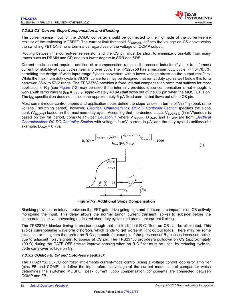
7.3.5.2 CS, Current Slope Compensation and Blanking
The current-sense input for the DC-DC converter should be connected to the high side of the current-senseresistor of the switching MOSFET. The current-limit threshold, VCSMAX, defines the voltage on CS above whichthe switching FET ON-time is terminated regardless of the voltage on COMP output.
Routing between the current-sense resistor and the CS pin must be short to minimize cross-talk from noisytraces such as DRAIN and CP, and to a lower degree to SRR and SRF.
Current-mode control requires addition of a compensation ramp to the sensed inductor (flyback transformer)current for stability at duty cycles near and over 50%. The TPS23758 has a maximum duty cycle limit of 78.5%,permitting the design of wide input-range flyback converters with a lower voltage stress on the output rectifiers.While the maximum duty cycle is 78.5%, converters may be designed that run at duty cycles well below this for anarrower, 36-V to 57-V range. The TPS23758 provides a fixed internal compensation ramp that suffices for mostapplications. RS (see Figure 7-2) may be used if the internally provided slope compensation is not enough. Itworks with ramp current (IPK = ISL-EX, approximately 40 μA) that flows out of the CS pin when the MOSFET is on.The IPK specification does not include the approximately 5-μA fixed current that flows out of the CS pin.
Most current-mode control papers and application notes define the slope values in terms of VPP/TS (peak rampvoltage / switching period); however, Electrical Characteristics: DC-DC Controller Section specifies the slopepeak (VSLOPE) based on the maximum duty cycle. Assuming that the desired slope, VSLOPE-D (in mV/period), isbased on the full period, compute R S per Equation 1 where V SLOPE, D MAX, and I SL-EX are from ElectricalCharacteristics: DC-DC Controller Section with voltages in mV, current in μA, and the duty cycle is unitless (forexample, DMAX = 0.78).
RS:3; =BVSLOPE _D:mV;F @VSLOPE (mV)
DMAXW AC
ISL EX(JA)/DMAX
× 1000
(1)
RSNS
CS
RT
N
GN
D
RS
RCS
DRAIN
CS
Figure 7-2. Additional Slope Compensation
Blanking provides an interval between the FET gate drive going high and the current comparator on CS activelymonitoring the input. This delay allows the normal turnon current transient (spike) to subside before thecomparator is active, preventing undesired short duty cycles and premature current limiting.
The TPS23758 blanker timing is precise enough that the traditional R-C filters on CS can be eliminated. Thisavoids current-sense waveform distortion, which tends to get worse at light output loads. There may be somesituations or designers that prefer an R-C approach, for example if the presence of RS causes increased noise,due to adjacent noisy signals, to appear at CS pin. The TPS23758 provides a pulldown on CS (approximately400 Ω) during the GATE OFF-time to improve sensing when an R-C filter must be used, by reducing cycle-to-cycle carry-over voltage on CS.
7.3.5.3 COMP, FB, CP and Opto-less Feedback
The TPS23758 DC-DC controller implements current-mode control, using a voltage control loop error amplifier(pins FB and COMP) to define the input reference voltage of the current mode control comparator whichdetermines the switching MOSFET peak current. Loop compensation components are connected betweenCOMP and FB.
TPS23758SLVSDW3A – APRIL 2019 – REVISED NOVEMBER 2020 www.ti.com
18 Submit Document Feedback Copyright © 2020 Texas Instruments Incorporated
Product Folder Links: TPS23758

V COMP below V ZDC causes the converter to stop switching. The maximum (peak) current is requested atapproximately (VZDC + 2 × (VCSMAX + VSLOPE)). The AC gain from COMP to the PWM comparator is 0.5.
The TPS23758 DC-DC controller can operate with feedback from an auxiliary winding of the flyback powertransformer, eliminating the need for external shunt regulator and optocoupler. It also operates with continuouslyconnected feedback, enabling better optimization of the power supply, and resulting in significantly lower noisesensitivity.
Opto-less operation of the TPS23758 is achieved with a unique approach which basically consists in cancellingthe leading-edge voltage overshoot (causing VCC to peak-charge) generated by the transformer winding. Whencombined with a correctly designed power transformer, less than ±2% load regulation over the full output currentrange becomes achievable in applications making use of secondary side synchronous rectifiers. Operation is incontinuous conduction mode (CCM), also enabling multi-output architectures.
7.3.5.4 FRS Frequency Setting and Synchronization
The FRS pin programs the (free-running) oscillator frequency, and may also be used to synchronize theTPS23758 converter to a higher frequency. The internal oscillator sets the maximum duty cycle and controls thecurrent-compensation ramp circuit, making the ramp height independent of frequency. RFRS must be selectedper Equation 2.
RFRS (k3) =15000
fSW (kHz)
(2)
The TPS23758 may be synchronized to an external clock to eliminate beat frequencies from a sampled system,or to place emission spectrum away from an RF input frequency. Synchronization may be accomplished byapplying a short pulse ( > 35 ns) of magnitude VSYNC to FRS as shown in Figure 7-3. RFRS must be chosen sothat the maximum free-running frequency is just below the desired synchronization frequency. Thesynchronization pulse terminates the potential ON-time period, and the OFF-time period does not begin until thepulse terminates. A short pulse is preferred to avoid reducing the potential ON-time.
Figure 7-3 shows examples of nonisolated and transformer-coupled synchronization circuits. RT reduces noisesusceptibility for the isolation transformer implementation. The FRS node must be protected from noise becauseit is high impedance.
FRS
RF
RS
47pF
Synchronization
Pulse
VSYNC
TSYNC
1:1
1000pF RT
RT
NFRS
RF
RS
47pF
Synchronization
Pulse
VSYNC
TSYNC
RT
N
Copyright © 2016, Texas Instruments Incorporated
Figure 7-3. Synchronization
7.3.5.5 Frequency Dithering for Spread Spectrum Applications
The international standard CISPR 22 (and adopted versions) is often used as a requirement for conductedemissions. Ethernet cables are covered as a telecommunication port under section 5.2 for conducted emissions.Meeting EMI requirements is often a challenge, with the lower limits of Class B being especially hard. Circuitboard layout, filtering, and snubbing various nodes in the power circuit are the first layer of control techniques. Amore detailed discussion of EMI control is presented in Practical Guidelines to Designing an EMI Compliant PoEPowered Device With Isolated Flyback, SLUA469. Additionally, IEEE 802.3at sections 33.3 and 33.4 haverequirements for noise injected onto the Ethernet cable based on compatibility with data transmission.
A technique referred to as frequency dithering can also be used to provide additional EMI measurementreduction. The switching frequency is modulated to spread the narrowband individual harmonics across a widerbandwidth, thus lowering peak measurements.
www.ti.comTPS23758
SLVSDW3A – APRIL 2019 – REVISED NOVEMBER 2020
Copyright © 2020 Texas Instruments Incorporated Submit Document Feedback 19
Product Folder Links: TPS23758

Frequency dithering is a built-in feature of the TPS23758. The oscillator frequency can be dithered byconnecting a capacitor from DTHR to RTN and a resistor from DTHR to FRS. An external capacitor, C DTR(Figure 8-1), is selected to define the modulation frequency fm. This capacitor is being continuously charged anddischarged between slightly less than 0.5 V and slightly above 1.5 V by a current source/sink equivalent toapproximately 3x the current through FRS pin. CDTR value is defined according to:
CDTR =
3RFRS (3)W
2.052 × fm (Hz)
(3)
fm should always be higher than 9 kHz, which is the resolution bandwidth applied during conducted emissionmeasurement. Typically, fm should be set to around 11 kHz to account for component variations.
The resistor R DTR is used to determine ∆f, which is the amount of dithering, and its value is determinedaccording to:
RDTR (3) =0.513 × RFRS (3)
%DTHR
(4)
For example, a 13.2% dithering with a nominal switching frequency of 250 kHz results in frequency variation of±33 kHz.
7.3.5.6 SST and Soft-Start of the Switcher
Converters require a soft-start on the voltage error amplifier to prevent output overshoot on startup. In PoEapplications, the PD also needs soft-start to limit its input current at turnon below the limit allocated by the powersource equipment (PSE).
The TPS23758 provides primary side closed loop controlled soft-start, which applies a slowly rising ramp voltageto a second control input of the error amplifier. The lower of the reference input and soft-start ramps controls theerror amplifier, allowing the output voltage to rise in a smooth monotonic fashion.
The soft-start period of the TPS23758 is adjustable with a capacitor between SST and RTN. During soft-start,CSST (Figure 8-1) is being charged from less than 0.2 V to 2.45 V by a ~4-µA current source. The actual controlrange of the closed loop soft-start capacitor voltage is between 0.25 V and 2 V nominally. Therefore, the soft-start capacitor value must be based on this control range and the required soft-start period (tSS) according to:
CSS =ISSC × tSS
(2 VF 0.25 V)
(5)
7.3.6 Internal Switching FET - DRAIN, RSNS, SRF and SRR
The DRAIN and RSNS provide connection to the drain and source of the integrated switching power FET. RSNSpin is a high current pin and it must have a short connection to the current sense resistor which other end isdirectly tied to a plane referenced to the GND pin. Current sensing is done with CS pin, which should beconnected directly to the high side of the current sense resistor.
The internal FET gate driver is powered from VB voltage rail and the return path is through the GND pin. SRFand SRR pins provide slew rate control of the switching FET. The gate sourcing current is drawn through theSRF pin which is tied to VB pin through a resistor (0-100 Ω). The gate sinking current circulates through the SRRpin which is externally tied to the GND pin either via a low-value resistor (0-15 Ω) or a direct connection.
7.3.7 VPD Supply Voltage
VPD pin connects to the positive side of the input supply. It provides operating power to the PD controller andallows monitoring of the input line voltage. If VVPD falls below its UVLO threshold and goes back above it, or if athermal shutdown resumes while V VPD is already above its UVLO threshold, the TPS23758 returns to inrushlimiting.
TPS23758SLVSDW3A – APRIL 2019 – REVISED NOVEMBER 2020 www.ti.com
20 Submit Document Feedback Copyright © 2020 Texas Instruments Incorporated
Product Folder Links: TPS23758

7.3.8 VDD Supply Voltage
VDD connects to the source of DC-DC converter startup current. It is connected to VPD for most applications. Itmay also be isolated by a diode from VPD to support some PoE priority operation.
7.3.9 GND
GND is the power ground used by the flyback power FET gate driver and CP pin. Connect to the RTN plane. VBbypassing capacitor should be directly connected to the GND pin.
7.3.10 VSS
VSS is the PoE input-power return side. It is the reference for the PoE interface circuits, and has a current-limited hotswap switch that connects it to RTN. VSS is clamped to a diode drop above RTN by the hotswapswitch. The exposed thermal PAD must be connected to this pin to ensure proper operation.
7.3.11 Exposed Thermal PAD
The exposed thermal PAD is internally connected to VSS pin. It should be tied to a large VSS copper area on thePCB to provide a low resistance thermal path to the circuit board. TI recommends maintaining a clearance of0.025” between VSS and high-voltage signals such as VPD and VDD.
7.4 Device Functional Modes7.4.1 PoE Overview
The following text is intended as an aid in understanding the operation of the TPS23758, but it is not a substitutefor the actual IEEE 802.3at standard. The IEEE 802.3at standard is an update to IEEE 802.3-2008 clause 33(PoE), adding high-power options and enhanced classification.
Generally speaking, a device compliant to IEEE 802.3-2008 is referred to as a Type 1 device, and devices withhigh power or enhanced classification is referred to as Type 2 devices. The TPS23758 is intended to power Type1 devices (up to 13 W), and is fully compliant to IEEE 802.3at for hardware classes 0 - 3. Standards change andmust always be referenced when making design decisions.
The IEEE 802.3at standard defines a method of safely powering a PD (powered device) over a cable, and thenremoving power if a PD is disconnected. The process proceeds through an idle state and three operationalstates of detection, classification, and operation. The PSE leaves the cable unpowered (idle state) while itperiodically looks to see if something has been plugged in; this is referred to as detection. The low power levelsused during detection are unlikely to damage devices not designed for PoE. If a valid PD signature is present,the PSE may inquire how much power the PD requires; this is referred to as (hardware) classification. Only Type2 PSEs are required to do hardware classification. The PD may return the default 13-W current-encoded class,or one of four other choices. The PSE may then power the PD if it has adequate capacity. Once started, the PDmust present the maintain power signature (MPS) to assure the PSE that it is still present. The PSE monitors itsoutput for a valid MPS, and turns the port off if it loses the MPS. Loss of the MPS returns the PSE to the idlestate. Figure 7-4 shows the operational states as a function of PD input voltage.
Normal Operation
5742363020.514.510.12.7
De
tec
tio
nL
ow
er
Lim
it
De
tec
tio
nU
pp
er
Lim
it
Cla
ss
ific
ati
on
Lo
we
rL
imit
Cla
ss
ific
ati
on
Up
pe
rL
imit
Mu
st
Tu
rnO
ffb
y-
Vo
lta
ge
Fa
llin
g
Lo
we
rL
imit
-P
rop
er
Op
era
tio
n
Mu
st
Tu
rnO
nb
y-
Vo
lta
ge
Ris
ing
Ma
xim
um
Inp
ut
Vo
lta
ge
Detect ClassifyShut-down
PI Voltage (V)
0
3/06/08
Figure 7-4. Operational States
www.ti.comTPS23758
SLVSDW3A – APRIL 2019 – REVISED NOVEMBER 2020
Copyright © 2020 Texas Instruments Incorporated Submit Document Feedback 21
Product Folder Links: TPS23758

The PD input is typically an RJ-45 eight-lead connector which is referred to as the power interface (PI). PD inputrequirements differ from PSE output requirements to account for voltage drops in the cable and operatingmargin. The IEEE 802.3at standard uses a cable resistance of 20 Ω for Type 1 devices to derive the voltagelimits at the PD based on the PSE output voltage requirements. Although the standard specifies an output powerof 15.4 W at the PSE, only 13 W is available at the PI due to the worst-case power loss in the cable. The PSEcan apply voltage either between the RX and TX pairs (pins 1–2 and 3–6 for 10baseT or 100baseT), or betweenthe two spare pairs (4–5 and 7–8). Power application to the same pin combinations in 1000baseT systems isrecognized in IEEE 802.3at. 1000baseT systems can handle data on all pairs, eliminating the spare pairterminology. The PSE may only apply voltage to one set of pairs at a time. The PD uses input diode bridges toaccept power from any of the possible PSE configurations. The voltage drops associated with the input bridgescreate a difference between the standard limits at the PI and the TPS23758 specifications.
The PSE is permitted to disconnect a PD if it draws more than its maximum class power over a one secondinterval. A Type 1 PSE compliant to IEEE 802.3at is required to limit current to between 400 mA and 450 mAduring powered operation, and it must disconnect the PD if it draws this current for more than 75 ms. Class 0and 3 PDs may draw up to 400-mA peak currents for up to 50 ms. The PSE may set lower output current limitsbased on the declared power requirements of the PD.
7.4.2 Threshold Voltages
The TPS23758 has a number of internal comparators with hysteresis for stable switching between the variousstates as shown in Figure 7-4. Figure 7-5 relates the parameters in Electrical Characteristics: DC-DC ControllerSection and Electrical Characteristics: PoE and Control to the PoE states. The mode labeled idle betweenclassification and operation implies that the DEN, CLS, and RTN pins are all high impedance.
VUVLO_R
Detection
Classification
PD Powered
Idle
VCL_ON
VCL_HYS
VCU_OFF
VCU_HYS
Note: Variable names refer to Electrical Characteristic Table parameters
VVPD-VVSS
VUVLO_H
Fu
nctio
na
l
Sta
te
1.4 V
Figure 7-5. Threshold Voltages
7.4.3 PoE Start-Up Sequence
The waveforms of Figure 7-6 demonstrate detection, classification, and start-up from a Type 1 PSE. The keywaveforms shown are VVPD-VSS, VRTN-VSS, and IPI. IEEE 802.3at requires a minimum of two detection levels;however, four levels are shown in this example. Four levels guard against misdetection of a device whenplugged in during the detection sequence.
TPS23758SLVSDW3A – APRIL 2019 – REVISED NOVEMBER 2020 www.ti.com
22 Submit Document Feedback Copyright © 2020 Texas Instruments Incorporated
Product Folder Links: TPS23758

Figure 7-6. PoE Start-Up Sequence
7.4.4 Detection
The TPS23758 is in detection mode whenever VVPD-V SS is below the lower classification threshold. When theinput voltage rises above V CL_ON, the DEN pin goes to an open-drain condition to conserve power. While indetection, RTN is high impedance, almost all the internal circuits are disabled, and the DEN pin is pulled to VSS.An RDEN of 24.9 kΩ (1%), presents the correct signature. It may be a small, low-power resistor because it onlysees a stress of about 5 mW. A valid PD detection signature is an incremental resistance between 23.75 kΩ and26.25 kΩ at the PI.
The detection resistance seen by the PSE at the PI is the result of the input bridge resistance in series with theparallel combination of R DEN and the TPS23758 bias loading. The incremental resistance of the input diodebridge may be hundreds of ohms at the very low currents drawn when 2.7 V is applied to the PI. The input bridgeresistance is partially cancelled by the effective resistance of the TPS23758 during detection.
7.4.5 Hardware Classification
Hardware classification allows a PSE to determine the power requirements of a PD before starting, and helpswith power management once power is applied. The maximum power entries in Table 7-1 determine the classthe PD must advertise. A Type 1 PD may not advertise Class 4. The PSE may disconnect a PD if it draws morethan its stated Class power. The standard permits the PD to draw limited current peaks; however, the averagepower requirement always applies.
Voltage from 14.5 V to 20.5 V is applied to the PD for up to 75 ms during hardware classification. A fixed outputvoltage is sourced by the CLS pin, causing a fixed current to be drawn from VPD through RCLS. The total currentdrawn from the PSE during classification is the sum of bias and R CLS currents. PD current is measured anddecoded by the PSE to determine which of the five available classes is advertised (see Table 7-1). TheTPS23758 disables classification above VCU_OFF to avoid excessive power dissipation. CLS voltage is turned offduring PD thermal limit or when APD or DEN are active . The CLS output is inherently current-limited, but shouldnot be shorted to VSS for long periods of time.
7.4.6 Maintain Power Signature (MPS)
The MPS is an electrical signature presented by the PD to assure the PSE that it is still present after operatingvoltage is applied. A valid MPS consists of a minimum DC current of 10 mA (at a duty cycle of at least 75 ms onevery 225 ms) and an AC impedance lower than 26.25 kΩ in parallel with 0.05 μF. The AC impedance is usuallyaccomplished by the minimum C BULK requirement of 5 μF. When APD or DEN is used to force the hotswap
www.ti.comTPS23758
SLVSDW3A – APRIL 2019 – REVISED NOVEMBER 2020
Copyright © 2020 Texas Instruments Incorporated Submit Document Feedback 23
Product Folder Links: TPS23758

switch off, the DC MPS is not met. A PSE that monitors the DC MPS will remove power from the PD when thisoccurs. A PSE that monitors only the AC MPS may remove power from the PD.
7.4.7 Start-Up and Converter Operation
The internal PoE undervoltage lockout (UVLO) circuit holds the hotswap switch off before the PSE provides fullvoltage to the PD. This prevents the converter circuits from loading the PoE input during detection andclassification. The converter circuits discharges CDD, CCC, and CVB while the PD is unpowered. Thus VVDD-RTNwill be a small voltage until just after full voltage is applied to the PD, as seen in Figure 7-6.
The PSE drives the PD input voltage to the operating range once it has decided to power up the PD. When VPDrises above the UVLO turnon threshold (VUVLO-R, approximately 35.5 V) with RTN high, the TPS23758 enablesthe hotswap MOSFET with an approximately 140-mA (inrush) current limit. See the waveforms of Figure 7-7 foran example. Converter switching is disabled while C DD charges and V RTN falls from V VDD to nearly V VSS;however, the converter start-up circuit is allowed to charge CCC. Once the inrush current falls about 10% belowthe inrush current limit, the PD control switches to the operational level (approximately 450 mA) and converterswitching is permitted.
Converter switching is allowed if the PD is not in inrush current limit and the VCC under-voltage lockout (VCUVR)circuit permits it. Continuing the start-up sequence shown in Figurer 7-7, V VCC rises as the start-up currentsource charges CCC and the converter switching is inhibited by the status of the VCC UVLO. The VB regulatorpowers the internal converter circuits as VVCC rises.
Once V VCC goes above its UVLO (nominally 8.25 V), the soft-start (SST) capacitor is first discharged withcontrolled current (I SSD) below nominally 0.2 V (V SFST) if the discharge was not already completed, then it isgradually recharged until it reaches ~0.25 V (VSSOFS) at which point the converter switching is enabled followingthe closed loop controlled soft-start sequence. Note that the startup current source capability is such that it canfully maintain VVCC during the converter soft-start without requiring any significant CCC capacitance, in 48 V inputapplications. At the end of the soft-start period, more specifically when SST voltage has exceeded ~2 V(V STUOF), the startup current source is turned off. V VCC falls as it powers the internal circuits including theswitching MOSFET gate. If the converter control-bias output rises to support V VCC before it falls to V CUVF(nominally 6.1 V), a successful start-up occurs. Figure 7-7 shows a small droop in VVCC while the output voltagerises smoothly and a successful start-up occurs.
TPS23758SLVSDW3A – APRIL 2019 – REVISED NOVEMBER 2020 www.ti.com
24 Submit Document Feedback Copyright © 2020 Texas Instruments Incorporated
Product Folder Links: TPS23758

Time: 10ms/div
1V/div
100mA/div IPI
Inrush
Converter
starts
VVDD-RTN
VSST
VVCC-RTN
5V/div
50V/div
PI powered
OUTPUT VOLTAGE
5V/div
VOUT
SOFT START
Startup turn off
Figure 7-7. Power Up and Start
The converter shuts off when VVCC falls below its lower UVLO. This can happen when power is removed fromthe PD, or during a fault on a converter output rail. When one output is shorted, all the output voltages fallincluding the one that powers VCC. The control circuit discharges VCC until it hits the lower UVLO and turns off.A restart initiates if the converter turns off and there is sufficient VDD voltage. This type of operation issometimes referred to as hiccup mode, which when combined with the soft-start provides robust output shortprotection by providing time-average heating reduction of the output rectifier.
Figure 7-8 illustrates the situation when there is severe overload at the main output which causes VCC hiccup.After VCC went below its UVLO due to the overload, the startup source is turned back on. Then, a new soft-startcycle is reinitiated, the soft-start capacitor being first discharged with controlled current, introducing a shortpause before the output voltage is ramped up.
www.ti.comTPS23758
SLVSDW3A – APRIL 2019 – REVISED NOVEMBER 2020
Copyright © 2020 Texas Instruments Incorporated Submit Document Feedback 25
Product Folder Links: TPS23758

Time: 10ms/div
1V/div
100mA/div
IPI
Converter
Turn off then restart
VSST
VVCC-RTN
5V/div
VOUT overload
OUTPUT VOLTAGE
5V/div
VOUT
SOFT START
Startup turn off
VCC
UVLO
Figure 7-8. Restart Following Severe Overload at Main Output of Flyback DC-DC Converter
If VVPD-VSS drops below the lower PoE UVLO (UVLO_R – UVLO_H, approximately 31 V), the hotswap MOSFETis turned off, but the converter still runs. The converter stops if VVCC falls below the VCUVF (nominally 6.1 V), thehotswap is in inrush current limit, the SST pin is pulled to ground, V VDD-RTN falls below typically 7.7 V(approximately 0.75 V hysteresis) or the converter is in thermal shutdown.
7.4.8 PD Self-Protection
The PD section has the following self-protection functions.
• Hotswap switch current limit• Hotswap switch foldback• Hotswap thermal protection
The internal hotswap MOSFET is protected against output faults with a current limit and deglitched foldback. ThePSE output cannot be relied on to protect the PD MOSFET against transient conditions, requiring the PD toprovide fault protection. High stress conditions include converter output shorts, shorts from VDD to RTN, ortransients on the input line. An overload on the pass MOSFET engages the current limit, with VRTN-VSS rising asa result. If VRTN rises above approximately 12.3 V for longer than approximately 400 μs, the current limit revertsto the inrush limit, and turns the converter off. The 400-μs deglitch feature prevents momentary transients fromcausing a PD reset, provided that recovery lies within the bounds of the hotswap and PSE protection. Figure 7-9shows an example of recovery from a 15-V PSE rising voltage step. The hotswap MOSFET goes into currentlimit, overshooting to a relatively low current, recovers to 420 mA, full-current limit, and charges the inputcapacitor while the converter continues to run. The MOSFET did not go into foldback because V RTN-VSS wasbelow 12 V after the 400-μs deglitch.
TPS23758SLVSDW3A – APRIL 2019 – REVISED NOVEMBER 2020 www.ti.com
26 Submit Document Feedback Copyright © 2020 Texas Instruments Incorporated
Product Folder Links: TPS23758

Time: 200us/div
200mA/div
IPI
CBULK completes
charge while converter
operates
VVSS-RTN § -15V
VVPD-VSS
10V/div
20V/div
Figure 7-9. Response to PSE Step Voltage
The PD control has a thermal sensor that protects the internal hotswap MOSFET. Conditions like start-up oroperation into a VPD to RTN short cause high power dissipation in the MOSFET. An overtemperature shutdown(OTSD) turns off the hotswap MOSFET and class regulator, which are restarted after the device cools. The PDrestarts in inrush current limit when exiting from a PD overtemperature event.
Pulling DEN to VSS during powered operation causes the internal hotswap MOSFET to turn off. This featureallows a PD with secondary-side adapter ORing to achieve adapter priority. Take care with synchronousconverter topologies that can deliver power in both directions.
The hotswap switch is forced off under the following conditions:
• VAPD above VAPDEN (approximately 1.5 V)• VDE N ≤ VPD_DIS when VVPD-VSS is in the operational range• PD over temperature• VVPD-VSS < PoE UVLO (approximately 31 V)
7.4.9 Adapter ORing
Many PoE-capable devices are designed to operate from either a wall adapter or PoE power. A local powersolution adds cost and complexity, but allows a product to be used if PoE is not available in a particularinstallation. While most applications only require that the PD operate when both sources are present, theTPS23758 device supports forced operation from either of the power sources. Figure 7-10 illustrates threeoptions for diode ORing external power into a PD. Only one option would be used in any particular design.Option 1 applies power to the device input, option 2 applies power between the device PoE section and thepower circuit, and option 3 applies power to the output side of the converter. Each of these options hasadvantages and disadvantages. Many of the basic ORing configurations and much of the discussion contained
www.ti.comTPS23758
SLVSDW3A – APRIL 2019 – REVISED NOVEMBER 2020
Copyright © 2020 Texas Instruments Incorporated Submit Document Feedback 27
Product Folder Links: TPS23758

in the application note Advanced Adapter ORing Solutions using the TPS23753, (SLVA306), apply to theTPS23758.
TP
S2
37
5858
V
0.1
uF
RD
EN
RC
LS
Fro
m E
the
rne
tT
ran
sfo
rme
rs
VP
D
VSS
CLSDEN
Low Voltage Output
RTN
Fro
m S
pa
re
Pa
irs o
r T
ran
sfo
rme
rs Power
Circuit
AdapterOption 3
AdapterOption 2
AdapterOption 1
VD
D
Figure 7-10. ORing Configurations
Preference of one power source presents a number of challenges. Combinations of adapter output voltage(nominal and tolerance), power insertion point, and which source is preferred determine solution complexity.Several factors contributing to the complexity are the natural high-voltage selection of diode ORing (the simplestmethod of combining sources), the current limit implicit in the PSE, PD inrush, and protection circuits (necessaryfor operation and reliability). Creating simple and seamless solutions is difficult if not impossible for many of thecombinations. However, the TPS23758 device offers several built-in features that simplify some combinations.
Several examples demonstrate the limitations inherent in ORing solutions. Diode ORing a 48-V adapter with PoE(option 1) presents the problem that either source might be higher. A blocking switch would be required to assurewhich source was active. A second example is combining a 12-V adapter with PoE using option 2. The converterdraws approximately four times the current at 12 V from the adapter than it does from PoE at 48 V. Transitionfrom adapter power to PoE may demand more current than can be supplied by the PSE. The converter must beturned off while CBULK capacitance charges, with a subsequent converter restart at the higher voltage and lowerinput current. A third example is use of a 12-V adapter with ORing option 1. The PD hotswap would have tohandle four times the current, and have 1/16 the resistance (be 16 times larger) to dissipate equal power. Afourth example is that MPS is lost when running from the adapter, causing the PSE to remove power from thePD. If adapter power is then lost, the PD stops operating until the PSE detects and powers the PD.
The most popular preferential ORing scheme is option 2 with adapter priority. The hotswap MOSFET is disabledwhen the adapter is used to pull APD high, blocking the PoE source from powering the output. This solutionworks well with a wide range of adapter voltages, is simple, and requires few external parts. When the AC powerfails, or the adapter is removed, the hotswap switch is enabled. In the simplest implementation, the PDmomentarily loses power until the PSE completes its start-up cycle.
The DEN pin can be used to disable the PoE input when ORing with option 3. This is an adapter priorityimplementation. Pulling DEN low, while creating an invalid detection signature, disables the hotswap MOSFET,and prevents the PD from redetecting. This would typically be accomplished with an optocoupler that is drivenfrom the secondary side of the converter.
The IEEE standards require that the PI conductors be electrically isolated from ground and all other systempotentials not part of the PI interface. The adapter must meet a minimum 1500-Vac dielectric withstand testbetween the output and all other connections for options 1 and 2. The adapter only needs this isolation for option3 if it is not provided by the converter.
TPS23758SLVSDW3A – APRIL 2019 – REVISED NOVEMBER 2020 www.ti.com
28 Submit Document Feedback Copyright © 2020 Texas Instruments Incorporated
Product Folder Links: TPS23758

Adapter ORing diodes are shown for all the options to protect against a reverse-voltage adapter, a short on theadapter input pins, and damage to a low-voltage adapter. ORing is sometimes accomplished with a MOSFET inoption 3.
www.ti.comTPS23758
SLVSDW3A – APRIL 2019 – REVISED NOVEMBER 2020
Copyright © 2020 Texas Instruments Incorporated Submit Document Feedback 29
Product Folder Links: TPS23758

8 Application and ImplementationNote
Information in the following applications sections is not part of the TI component specification, and TIdoes not warrant its accuracy or completeness. TI’s customers are responsible for determiningsuitability of components for their purposes. Customers should validate and test their designimplementation to confirm system functionality.
8.1 Application InformationThe TPS23758 supports power supply topologies that require a single PWM gate drive with current-modecontrol. Figure 8-1 provides an example of a synchronous FET rectified primary-side-regulated flyback converter.
8.2 Typical Application
Figure 8-1. Basic TPS23758 Implementation
8.2.1 Design Requirements
Selecting a converter topology along with a design procedure is beyond the scope of this applications section.The TPS23758 is optimized for primary-side-regulated synchronous FET rectified flyback topologies of 5 V orlower due to its good balance of high efficiency and output regulation. Typical applications use post regulation topower the system load's lower voltage rails whereas the TPS23758 allows the elimination of a post regulatedconverter like shown in Figure 8-1 . The TPS23758 can also be used in non-isolated buck topology applicationlike shown in Figure 8-1.
Examples to help in programming the TPS23758 in a primary-side regulated flyback are shown below. For morespecific converter design examples refer to the TPS23758EVM-080EVM: Evaluation Module for TPS23758.
Table 8-1. Design ParametersPARAMETER TEST CONDITIONS MIN TYP MAX UNITPOWER INTERFACEInput voltage Applied to the PoE Input 37 57 V
Applied to Primary Adapter Input 48 V
TPS23758SLVSDW3A – APRIL 2019 – REVISED NOVEMBER 2020 www.ti.com
30 Submit Document Feedback Copyright © 2020 Texas Instruments Incorporated
Product Folder Links: TPS23758

Table 8-1. Design Parameters (continued)PARAMETER TEST CONDITIONS MIN TYP MAX UNITDetection voltage At device terminals 2.7 10.1 V
Classification voltage At device terminals 14.5 20.5 V
Classification 3
Inrush current-limit 140 mA
Operating current-limit 550 mA
DC-TO-DC CONVERTEROutput voltage VIN = 48 V, ILOAD ≤ ILOAD (max) 5 V
Output current 37 V ≤ VIN ≤ 57 V 2.3 A
Output ripple voltage peak-to-peak VIN = 48 V, ILOAD = 1 A 34 mV
Efficiency, end-to-end
VIN = 48 V, ILOAD= 230 mA 61
%VIN = 48 V, ILOAD = 1.15 A 85
VIN = 48 V, ILOAD = 2.3 A 88
Switching frequency 250 kHz
8.2.2 Detailed Design Procedure8.2.2.1 Input Bridges and Schottky Diodes
Using Schottky diodes instead of PN junction diodes for the PoE input bridges reduces the power dissipation inthese devices by about 30%. There are, however, some things to consider when using them. The IEEE standardspecifies a maximum backfeed voltage of 2.8 V. A 100-kΩ resistor is placed between the unpowered pairs andthe voltage is measured across the resistor. Schottky diodes often have a higher reverse leakage current thanPN diodes, making this a harder requirement to meet. To compensate, use conservative design for diodeoperating temperature, select lower-leakage devices where possible, and match leakage and temperatures byusing packaged bridges.
Schottky diode leakage currents and lower dynamic resistances can impact the detection signature. Settingreasonable expectations for the temperature range over which the detection signature is accurate is the simplestsolution. Increasing RDEN slightly may also help meet the requirement.
Schottky diodes have proven less robust to the stresses of ESD transients than PN junction diodes. Afterexposure to ESD, Schottky diodes may become shorted or leak. Care must be taken to provide adequateprotection in line with the exposure levels. This protection may be as simple as ferrite beads and capacitors.
As a general recommendation, use 0.8 A-1 A, 100-V rated discrete or bridge diodes for the input rectifiers.
8.2.2.2 Softstart Capacitor, Css
An approximately 10-ms softstart period is recommended, so using Equation 5, a 22-nF softstart capacitor (Css)is used
8.2.2.3 Protection, D1
A TVS, D 1, across the rectified PoE voltage per Figure 8-1 must be used. A SMAJ58A, or equivalent, isrecommended for general indoor applications. Adequate capacitive filtering or a TVS must limit input transientvoltage to within the absolute maximum ratings. Outdoor transient levels or special applications requireadditional protection.
8.2.2.4 Capacitor, C1
The IEEE 802.3at standard specifies an input bypass capacitor (from VDD to VSS) of 0.05 μF to 0.12 μF.Typically a 0.1-μF, 100-V, 10% ceramic capacitor is used.
8.2.2.5 Detection Resistor, RDEN
The IEEE 802.3at standard specifies a detection signature resistance, RDEN between 23.7 kΩ and 26.3 kΩ, or 25kΩ ± 5%. Typically a 24.9 kΩ ± 1% is used.
www.ti.comTPS23758
SLVSDW3A – APRIL 2019 – REVISED NOVEMBER 2020
Copyright © 2020 Texas Instruments Incorporated Submit Document Feedback 31
Product Folder Links: TPS23758
8.2.2.6 Classification Resistor
Connect a resistor from CLS to VSS to program the classification current according to the IEEE 802.3atstandard. The class power assigned should correspond to the maximum average power drawn by the PD duringoperation. Select RCLS according to Table 7-1.
8.2.2.7 Bulk Capacitance, CBULK
The bulk capacitance, CBULK must furnish input transients during heavy loads and long cable length conditions. Italso helps with stability on the DC/DC converter. It is recommended to use a minimum 10-uF, electrolyticcapacitor.
8.2.2.8 Output Voltage Feedback Divider, RAUX, R1,R2
R1, R2 and set the output voltage of the bias winding of the converter.
REFC 1 2
VCC
2
V R RV
R (6)
when Aux_D is LOW.
when Aux_D is HIGH.
8.2.2.9 Setting Frequency, RFRS
The converter switching frequency in PWM mode is set by connecting resistor, RFRS from the FRS pin to RTN.For a converter that requires a 250-kHz switching frequency and using Equation 7
FRS
SW
15000 15000R k 60 k
250 kHzf kHz: :
(7)
A standard 60.4-kΩ resistor should be used.
8.2.2.10 Frequency Dithering, RDTR and CDTR
For optimum EMI performance, C DTR and R DTR should be selected as described in Frequency Dithering forSpread Spectrum Applications in Equation 8 and Equation 9.
: :
uu
FRS
DTR
m
3 3R 60.4 k
C nF 2.2 nF2.052 11000 Hz2.052 f Hz (8)
FRS
DTR
0.513 R 0.513 60.4kR 235 k
%DTHR 0.132
u : u :: :
(9)
A standard 237-kΩ resistor should be used.
8.2.2.11 Bias Voltage, CVB and DVB
VB requires a 0.1 μF capacitor, CVB, to RTN. DVB , a 6.2V Zener diode to RTN, is also required.
Note: DVB on VB is optional in 13W applications when no class resistor is used.
8.2.2.12 Transformer design, T1
The turns ratio and primary inductance are important parameters to consider in a flyback transformer. The turnsratio act to limit the max duty cycle and reduce stress on the secondary components while the primary
TPS23758SLVSDW3A – APRIL 2019 – REVISED NOVEMBER 2020 www.ti.com
32 Submit Document Feedback Copyright © 2020 Texas Instruments Incorporated
Product Folder Links: TPS23758

inductance sets the current ripple. In CCM operation, the higher inductance allows for a reduced current ripplewhich can help with EMI performance and noise.
For primary-side regulated flyback converters, the transformer construction is important to maintain goodregulation on the secondary output. It is recommended to use LDT1018 for 5-V applications.
8.2.2.13 Current Sense Resistor, RCS
RCS should be chosen based on the peak primary current at the desired output current limit.
CSMAX
CS
Pk Pr imary
VR
I
(10)
8.2.2.14 Current Slope Compensation, RS
RS may be used if the internally provided slope compensation is not enough. The down slope of the reflectedsecondary current through the current sense resistor at each switching period is determined and a percentage(typically 50%-75%) of it will define Vslope. If necessary, using LDT1018, it is recommended to start with 251 mVand use Equation 11.
D
EX
SLOPE
SLOPE
MAX
S
SL
MAX
V mV155 mVV mV 251mV
D 78.5%R 1000 1000 1k
42 AI A
78.5%D
ª º§ · ª º§ ·« » ¨ ¸ « »¨ ¸¨ ¸« »© ¹ © ¹¬ ¼ ¬ ¼: u u :PP
(11)
8.2.2.15 Bias Supply Requirements, CCC, DCC
Advanced startup in the TPS23758 allows for relatively low capacitance on the bias circuit. It is recommended touse a 1-uF, 10%, 25-V ceramic capacitors on C CC. D CC can be a low cost, general-purpose diode. It isrecommended to use MMSD4148 diode (100 V, 200 mA).
8.2.2.16 Switching Transformer Considerations, RVCC and CCC2
R VCC helps to reduce peak charging from the bias winding. Reduced peak charging becomes especiallyimportant when tuning hiccup mode operation during output overload. A typical value for RVCC in Type 1 PoE PDapplications while maintaining a suitable load regulation is 10 ohms.
8.2.2.17 Primary FET Clamping, RCL, CCL, and DCL
The stored energy in the leakage inductance of the power transformer can cause ringing during the primary FETturnoff. The snubber must be chosen to mitigate primary FET overshoot and oscillation while maintaining highoverall efficiency.
It is recommended to use 39 kΩ (125 mW) for RCL and 0.1 uF (100 V) for CCL.
DCL should be an ultra-fast diode with a short forward recovery time allowing the snubber to turn on quickly. The200-V / 1-A rated diode with a recovery time approximately 25 ns or better is recommended.
8.2.2.18 Converter Output Capacitance, COUT
The output capacitor is considered as part of the overall stability of the converter, the output voltage ripple, andthe load transient response. The output capacitor needs to be selected based on the most stringent of thesecriteria. The minimum capacitance is typically determined by the output voltage ripple shown in Equation 12.
OUT max
OUT
Ripple SW
I A DC
V V f Hz
u!
u (12)
www.ti.comTPS23758
SLVSDW3A – APRIL 2019 – REVISED NOVEMBER 2020
Copyright © 2020 Texas Instruments Incorporated Submit Document Feedback 33
Product Folder Links: TPS23758

where Dmax is the calculated operating max duty cycle shown in Equation 13.
OUT PS
max
IN OUT PS
V ND
V min V N
u
u(13)
For strict load transient requirements, the COUT cap may need to be increased. The TPS23758EVM-080 usesthree 100 uF ceramic capacitors for an optimized load transient response.
8.2.2.19 Synchronous Rectifier, QR
The output synchronous FET rectifier must have a small Rds(on) and total gate charge (Qc). Consideration mustbe given to a safe operating area during output overload conditions.
For a 5-V output, CSD17579Q3A in a high thermal performance package (30-V reverse voltage, 11-A continuousdrain current max, 11.5-nC total gate charge @ 10 Vgs) is used in the TPS23758EVM-080
Some synchronous flyback topologies in certain operating conditions can benefit from added protection acrossthe synchronous FET. It is recommended to add a zener DR across the synch FET that can be populated whenneeded.
8.2.2.20 Synchronous Rectifier Clamp, DZ
DZ clamps the gate voltage of the synchronous rectifier. It is recommended to use two MMSZ5242B-7-F zenerdiodes (12 V, 500 mW) for DZ.
8.2.2.21 Synchronous Rectifier Gate Diode, DG
DG is used for fast turn off of the synchronous rectifier. It is recommended to use MMSD4148T1G (100 V, 200mA, SOD-123) for DG.
8.2.2.22 Sync Rectifier Slew Rate Control, RG
RG is used to adjust the turn on slew rate of the synchronous rectifier. It is recommended to use a 10 Ω resistorin an 0402 package with a 63-mW power rating
8.2.2.23 Slew rate control, RSRF and RSRR
R SRF and R SRR minimize primary drain-source oscillations and help optimize EMI performance at highfrequencies, the value chosen should be within the recommend operating conditions table in RecommendedOperating Conditions. It is recommended to start with 10 ohms for R SRF and 10 ohms for R SRR then adjustaccordingly during bench and EMI testing.
8.2.2.24 Shutdown at Low Temperatures, DVDD and CVDD
For applications operating near –10°C or less, there may be some extra switching cycles during removal of thePoE input or during shutdown. It is acceptable for most applications; however, for a more monotonic shutdown ofthe output voltage during power removal, it is recommended to use D VDD and C VDD as shown in Figure 8-2.DVDD can be MMSD4148 and CVDD can be 0.22-uF, 100-V capacitor.
TPS23758SLVSDW3A – APRIL 2019 – REVISED NOVEMBER 2020 www.ti.com
34 Submit Document Feedback Copyright © 2020 Texas Instruments Incorporated
Product Folder Links: TPS23758

TPS23755
Fro
m E
the
rne
tT
ran
sfo
rme
rsVPD
VSS
Fro
m S
pa
re P
airs
or
Tra
nsfo
rme
rsVDD
D1
DVDD
C1
CBULK
+
CVDD
Figure 8-2. DVDD and CVDD Configuration for Low Temperature Conditions
8.2.3 Application Curves
Figure 8-3. TPS23758 Startup to TPS23880 PSE Figure 8-4. TPS23758 PSR Flyback Startup to FullLoad
Figure 8-5. TPS23758 Output Short and Recovery Figure 8-6. Slew Rate Adjust SRR = 10 Ω
www.ti.comTPS23758
SLVSDW3A – APRIL 2019 – REVISED NOVEMBER 2020
Copyright © 2020 Texas Instruments Incorporated Submit Document Feedback 35
Product Folder Links: TPS23758
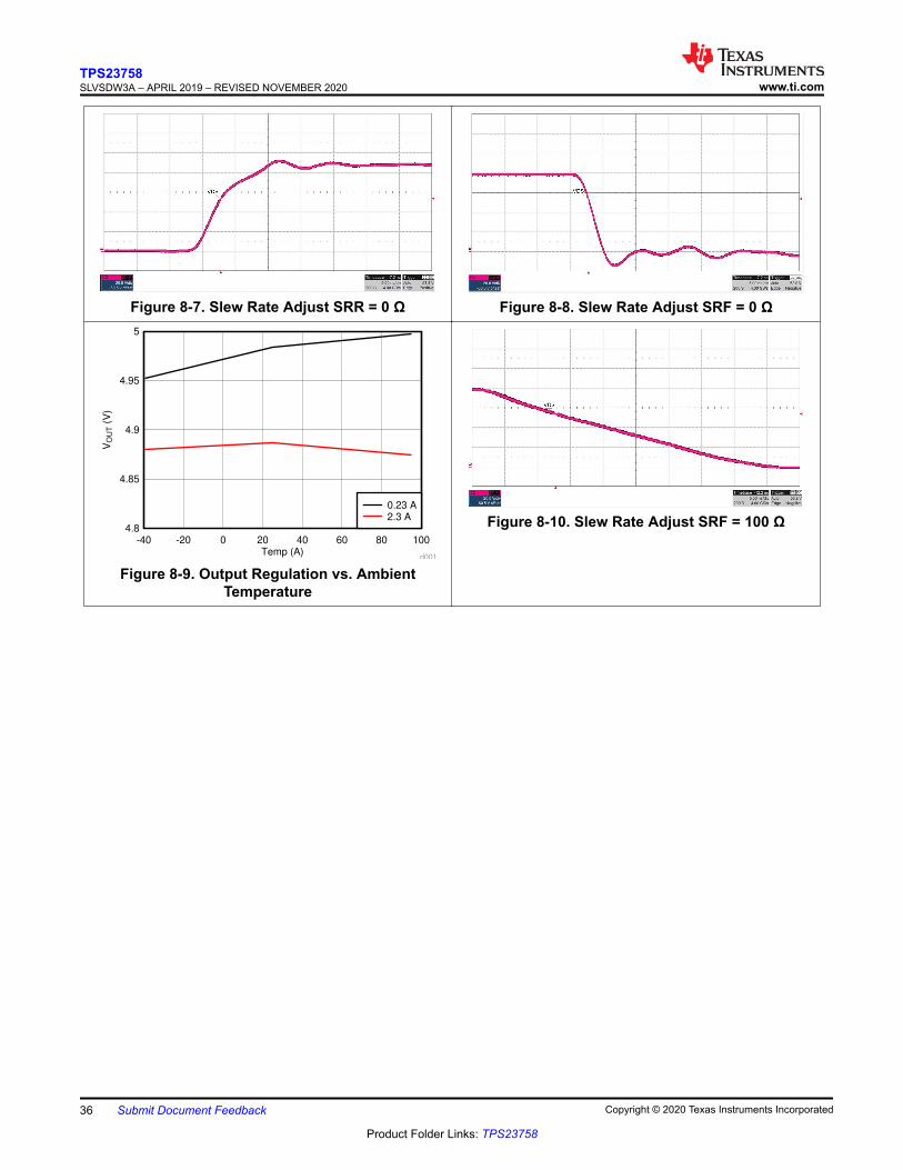
Figure 8-7. Slew Rate Adjust SRR = 0 Ω Figure 8-8. Slew Rate Adjust SRF = 0 Ω
Temp (A)
VO
UT (
V)
-40 -20 0 20 40 60 80 1004.8
4.85
4.9
4.95
5
d001
0.23 A2.3 A
Figure 8-9. Output Regulation vs. AmbientTemperature
Figure 8-10. Slew Rate Adjust SRF = 100 Ω
TPS23758SLVSDW3A – APRIL 2019 – REVISED NOVEMBER 2020 www.ti.com
36 Submit Document Feedback Copyright © 2020 Texas Instruments Incorporated
Product Folder Links: TPS23758

9 Power Supply RecommendationsThe TPS23758 converter should be designed such that the input voltage of the converter is capable of operatingwithin the IEEE802.3at recommended input voltage as shown in Figure 7-4 and the minimum operating voltageof the adapter if applicable.
10 Layout10.1 Layout GuidelinesThe TPS23758 IC’s layout footprint shown in the Example Board Layout should be strictly followed. The belowlist are key highlights for layout consideration around the TPS23758.
• Pin 22 of the TPS23758 is omitted from the IC to ensure high voltage clearance from Pin 24 (DRAIN).Therefore, the Pin 22 footprint should be removed when laying out the TPS23758.
• It is recommended having at least 8 vias (VSS) connecting the exposed thermal pad through a top layerplane (2 oz copper recommended) to a bottom VSS plane (2 oz. copper recommended) to help with thermaldissipation.
• The Pin24 of the TPS23758 should be near the power transformer and the current sense resistor should beclose to Pin 1 of the TPS23758 to minimize the primary loop.
The layout of the PoE front end should follow power and EMI or ESD best-practice guidelines. A basic set ofrecommendations includes:• Parts placement must be driven by power flow in a point-to-point manner; RJ-45, Ethernet transformer, diode
bridges, TVS and 0.1-μF capacitor, and TPS23758 converter input bulk capacitor.• Make all leads as short as possible with wide power traces and paired signal and return.• No crossovers of signals from one part of the flow to another are allowed.• Spacing consistent with safety standards like IEC60950 must be observed between the 48-V input voltage
rails and between the input and an isolated converter output.• Use large copper fills and traces on SMT power-dissipating devices, and use wide traces or overlay copper
fills in the power path.
The DC-to-DC converter layout benefits from basic rules such as:• Having at least 4 vias (VDD) near the power transformer pin connected to VDD through multiple layer planes
to help with thermal dissipation of the power transformer.• Having at least 6 vias (secondary ground) near the power transformer pin connected to secondary ground
through multiple layer planes to help with thermal dissipation of the power transformer.• Pair signals to reduce emissions and noise, especially the paths that carry high-current pulses, which include
the power semiconductors and magnetics.• Minimize the trace length of high current power semiconductors and magnetic components.• Where possible, use vertical pairing.• Use the ground plane for the switching currents carefully.• Keep the high-current and high-voltage switching away from low-level sensing circuits including those outside
the power supply.• Maintain proper spacing around the high-voltage sections of the converter.
10.2 Layout ExampleFigure 10-1 and Figure 10-2 show the top and bottom layer and assemblies of the TPS23758EVM-080 as areference for optimum parts placement.
www.ti.comTPS23758
SLVSDW3A – APRIL 2019 – REVISED NOVEMBER 2020
Copyright © 2020 Texas Instruments Incorporated Submit Document Feedback 37
Product Folder Links: TPS23758

Figure 10-1. Top Side and Routing
Figure 10-2. Bottom Side Placement and Routing
TPS23758SLVSDW3A – APRIL 2019 – REVISED NOVEMBER 2020 www.ti.com
38 Submit Document Feedback Copyright © 2020 Texas Instruments Incorporated
Product Folder Links: TPS23758

11 Device and Documentation Support11.1 Related documentationFor related documentation, see the following:
• Texas Instruments, Practical Guidelines to Designing an EMI-Compliant PoE Powered Device With IsolatedFlyback, application report
• Texas Instruments, TPS23758EVM-080: Evaluation Module, user's guide
11.2 Support ResourcesTI E2E™ support forums are an engineer's go-to source for fast, verified answers and design help — straightfrom the experts. Search existing answers or ask your own question to get the quick design help you need.
Linked content is provided "AS IS" by the respective contributors. They do not constitute TI specifications and donot necessarily reflect TI's views; see TI's Terms of Use.
11.3 TrademarksTI E2E™ is a trademark of Texas Instruments.All trademarks are the property of their respective owners.11.4 Electrostatic Discharge Caution
This integrated circuit can be damaged by ESD. Texas Instruments recommends that all integrated circuits be handledwith appropriate precautions. Failure to observe proper handling and installation procedures can cause damage.ESD damage can range from subtle performance degradation to complete device failure. Precision integrated circuits maybe more susceptible to damage because very small parametric changes could cause the device not to meet its publishedspecifications.
11.5 GlossaryTI Glossary This glossary lists and explains terms, acronyms, and definitions.
12 Mechanical, Packaging, and Orderable InformationThe following pages include mechanical, packaging, and orderable information. This information is the mostcurrent data available for the designated devices. This data is subject to change without notice and revision ofthis document. For browser-based versions of this data sheet, refer to the left-hand navigation.
www.ti.comTPS23758
SLVSDW3A – APRIL 2019 – REVISED NOVEMBER 2020
Copyright © 2020 Texas Instruments Incorporated Submit Document Feedback 39
Product Folder Links: TPS23758

12.1 Package Option Addendum
Packaging InformationOrderable Device Status (1) Package
TypePackageDrawing Pins Package
Qty Eco Plan (2) Lead/BallFinish(4) MSL Peak Temp (3) Op Temp (°C) Device Marking(5) (6)
PTPS23758RJJR ACTIVE VSON RJJ 23 3000 TBD Call TI Call TI –40 to 125 PPS23758
TPS23758RJJR ACTIVE VSON RJJ 23 3000 Green (RoHS& no Sb/Br) CU NIPDAU Level-2-260C-1 YEAR –40 to 125 TPS23758
TPS23758RJJR ACTIVE VSON RJJ 23 250 Green (RoHS& no Sb/Br) CU NIPDAU Level-2-260C-1 YEAR –40 to 125 TPS23758
(1) The marketing status values are defined as follows:ACTIVE: Product device recommended for new designs.LIFEBUY: TI has announced that the device will be discontinued, and a lifetime-buy period is in effect.NRND: Not recommended for new designs. Device is in production to support existing customers, but TI does not recommend using this part in a new design.PRE_PROD Unannounced device, not in production, not available for mass market, nor on the web, samples not available.PREVIEW: Device has been announced but is not in production. Samples may or may not be available.OBSOLETE: TI has discontinued the production of the device.space
(2) Eco Plan - The planned eco-friendly classification: Pb-Free (RoHS), Pb-Free (RoHS Exempt), or Green (RoHS & no Sb/Br) - please check http://www.ti.com/productcontent for the latestavailability information and additional product content details.TBD: The Pb-Free/Green conversion plan has not been defined.Pb-Free (RoHS): TI's terms "Lead-Free" or "Pb-Free" mean semiconductor products that are compatible with the current RoHS requirements for all 6 substances, including therequirement that lead not exceed 0.1% by weight in homogeneous materials. Where designed to be soldered at high temperatures, TI Pb-Free products are suitable for use in specifiedlead-free processes.Pb-Free (RoHS Exempt): This component has a RoHS exemption for either 1) lead-based flip-chip solder bumps used between the die and package, or 2) lead-based die adhesive usedbetween the die and leadframe. The component is otherwise considered Pb-Free (RoHS compatible) as defined above.Green (RoHS & no Sb/Br): TI defines "Green" to mean Pb-Free (RoHS compatible), and free of Bromine (Br) and Antimony (Sb) based flame retardants (Br or Sb do not exceed 0.1%by weight in homogeneous material)space
(3) MSL, Peak Temp. -- The Moisture Sensitivity Level rating according to the JEDEC industry standard classifications, and peak solder temperature.space
(4) Lead/Ball Finish - Orderable Devices may have multiple material finish options. Finish options are separated by a vertical ruled line. Lead/Ball Finish values may wrap to two lines if thefinish value exceeds the maximum column width.space
(5) There may be additional marking, which relates to the logo, the lot trace code information, or the environmental category on the devicespace
(6) Multiple Device markings will be inside parentheses. Only one Device Marking contained in parentheses and separated by a "~" will appear on a device. If a line is indented then it is acontinuation of the previous line and the two combined represent the entire Device Marking for that device.
Important Information and Disclaimer: The information provided on this page represents TI's knowledge and belief as of the date that it is provided. TI bases its knowledge and belief on information provided bythird parties, and makes no representation or warranty as to the accuracy of such information. Efforts are underway to better integrate information from third parties. TI has taken and continues to take reasonablesteps to provide representative and accurate information but may not have conducted destructive testing or chemical analysis on incoming materials and chemicals. TI and TI suppliers consider certaininformation to be proprietary, and thus CAS numbers and other limited information may not be available for release.
In no event shall TI's liability arising out of such information exceed the total purchase price of the TI part(s) at issue in this document sold by TI to Customer on an annual basis.
TPS23758SLVSDW3A – APRIL 2019 – REVISED NOVEMBER 2020 www.ti.com
40 Submit Document Feedback Copyright © 2020 Texas Instruments Incorporated
Product Folder Links: TPS23758

www.ti.com
PACKAGE OUTLINE
C
23X0.250.15
1.9 0.1
23X0.50.3
1 MAX
(0.2) TYP
0.050.00
20X 0.4
2X
4.4
2X (1.6)
8X (0.4)
5.5 0.1
10X (0.2)
B4.13.9
A
6.15.9
4X (0.4)
4X ( 0.25)
4X (0.45)
VSON - 1 mm max heightRJJ0023BPLASTIC QUAD FLATPACK - NO LEAD
4223621/B 06/2017
PIN 1 INDEX AREA
0.08 C
SEATING PLANE
1
1213
24
PIN 1 ID
0.1 C B A
0.05
EXPOSEDTHERMAL PAD
SYMM
SYMM
A1
A2 A3
A4
25
NOTES:
1. All linear dimensions are in millimeters. Any dimensions in parenthesis are for reference only. Dimensioning and tolerancingper ASME Y14.5M.
2. This drawing is subject to change without notice.3. The package thermal pad must be soldered to the printed circuit board for thermal and mechanical performance.
0.08
SCALE 2.500
www.ti.comTPS23758
SLVSDW3A – APRIL 2019 – REVISED NOVEMBER 2020
Copyright © 2020 Texas Instruments Incorporated Submit Document Feedback 41
Product Folder Links: TPS23758

www.ti.com
EXAMPLE BOARD LAYOUT
0.05 MINALL AROUND
0.05 MAXALL AROUND
20X (0.4)
23X (0.6)
23X (0.2)
( 0.2) TYPVIA
(R0.05) TYPALL PAD CORNERS
(2)
(1.9)
10X (0.2)
4X ( 0.25)
(3.8)
4X (1.725)
8X(0.4)
(5.5)
(0.45) TYP
4X (2.675)
(1.32)TYP
(0.6)TYP
VSON - 1 mm max heightRJJ0023BPLASTIC QUAD FLATPACK - NO LEAD
4223621/B 06/2017
NOTES: (continued)
4. This package is designed to be soldered to a thermal pad on the board. For more information, see Texas Instruments literaturenumber SLUA271 (www.ti.com/lit/slua271).
5. Vias are optional depending on application, refer to device data sheet. If any vias are implemented, refer to their locations shownon this view. It is recommended that vias under paste be filled, plugged or tented.
SOLDER MASKOPENING
METAL UNDERSOLDER MASK
SOLDER MASKDEFINED
EXPOSEDMETAL
METAL
SOLDER MASKOPENING
NON SOLDER MASK
SOLDER MASK DETAILS
DEFINED(PREFERRED)
EXPOSEDMETAL
SYMM
1
12 13
24
SYMM
A1
A2A3
A4
25
EXPOSED METAL SHOWNLAND PATTERN EXAMPLE
SCALE: 15X
METAL UNDERSOLDER MASK
SOLDER MASKOPENING
TPS23758SLVSDW3A – APRIL 2019 – REVISED NOVEMBER 2020 www.ti.com
42 Submit Document Feedback Copyright © 2020 Texas Instruments Incorporated
Product Folder Links: TPS23758

www.ti.com
EXAMPLE STENCIL DESIGN
23X (0.6)
23X (0.2)
20X (0.4)
(3.8)
8X (0.85)
(R0.05) TYP
4X (2.675)
4X ( 0.25)
(0.66) TYP
(1.32) TYP
(0.525) TYP
8X (1.12)
10X (0.46)
(5.94)
4X (1.725)
VSON - 1 mm max heightRJJ0023BPLASTIC QUAD FLATPACK - NO LEAD
4223621B 06/2017
NOTES: (continued)
6. Laser cutting apertures with trapezoidal walls and rounded corners may offer better paste release. IPC-7525 may have alternatedesign recommendations.
A1
A2 A3
A4
SYMM
OPENINGSOLDER MASK
BASED ON 0.1 mm THICK STENCILSOLDER PASTE EXAMPLE
PRINTED SOLDER COVERAGE BY AREA UNDER PACKAGETHERMAL PAD 25: 73%
SCALE:20X
SYMM
1
12 13
24
25
METAL UNDERSOLDER MASK
www.ti.comTPS23758
SLVSDW3A – APRIL 2019 – REVISED NOVEMBER 2020
Copyright © 2020 Texas Instruments Incorporated Submit Document Feedback 43
Product Folder Links: TPS23758

PACKAGE OPTION ADDENDUM
www.ti.com 10-Dec-2020
Addendum-Page 1
PACKAGING INFORMATION
Orderable Device Status(1)
Package Type PackageDrawing
Pins PackageQty
Eco Plan(2)
Lead finish/Ball material
(6)
MSL Peak Temp(3)
Op Temp (°C) Device Marking(4/5)
Samples
TPS23758RJJR ACTIVE VSON RJJ 23 3000 RoHS & Green NIPDAUAG Level-2-260C-1 YEAR -40 to 125 TPS23758
TPS23758RJJT ACTIVE VSON RJJ 23 250 RoHS & Green NIPDAUAG Level-2-260C-1 YEAR -40 to 125 TPS23758
(1) The marketing status values are defined as follows:ACTIVE: Product device recommended for new designs.LIFEBUY: TI has announced that the device will be discontinued, and a lifetime-buy period is in effect.NRND: Not recommended for new designs. Device is in production to support existing customers, but TI does not recommend using this part in a new design.PREVIEW: Device has been announced but is not in production. Samples may or may not be available.OBSOLETE: TI has discontinued the production of the device.
(2) RoHS: TI defines "RoHS" to mean semiconductor products that are compliant with the current EU RoHS requirements for all 10 RoHS substances, including the requirement that RoHS substancedo not exceed 0.1% by weight in homogeneous materials. Where designed to be soldered at high temperatures, "RoHS" products are suitable for use in specified lead-free processes. TI mayreference these types of products as "Pb-Free".RoHS Exempt: TI defines "RoHS Exempt" to mean products that contain lead but are compliant with EU RoHS pursuant to a specific EU RoHS exemption.Green: TI defines "Green" to mean the content of Chlorine (Cl) and Bromine (Br) based flame retardants meet JS709B low halogen requirements of <=1000ppm threshold. Antimony trioxide basedflame retardants must also meet the <=1000ppm threshold requirement.
(3) MSL, Peak Temp. - The Moisture Sensitivity Level rating according to the JEDEC industry standard classifications, and peak solder temperature.
(4) There may be additional marking, which relates to the logo, the lot trace code information, or the environmental category on the device.
(5) Multiple Device Markings will be inside parentheses. Only one Device Marking contained in parentheses and separated by a "~" will appear on a device. If a line is indented then it is a continuationof the previous line and the two combined represent the entire Device Marking for that device.
(6) Lead finish/Ball material - Orderable Devices may have multiple material finish options. Finish options are separated by a vertical ruled line. Lead finish/Ball material values may wrap to twolines if the finish value exceeds the maximum column width.
Important Information and Disclaimer:The information provided on this page represents TI's knowledge and belief as of the date that it is provided. TI bases its knowledge and belief on informationprovided by third parties, and makes no representation or warranty as to the accuracy of such information. Efforts are underway to better integrate information from third parties. TI has taken andcontinues to take reasonable steps to provide representative and accurate information but may not have conducted destructive testing or chemical analysis on incoming materials and chemicals.TI and TI suppliers consider certain information to be proprietary, and thus CAS numbers and other limited information may not be available for release.
In no event shall TI's liability arising out of such information exceed the total purchase price of the TI part(s) at issue in this document sold by TI to Customer on an annual basis.

PACKAGE OPTION ADDENDUM
www.ti.com 10-Dec-2020
Addendum-Page 2

TAPE AND REEL INFORMATION
*All dimensions are nominal
Device PackageType
PackageDrawing
Pins SPQ ReelDiameter
(mm)
ReelWidth
W1 (mm)
A0(mm)
B0(mm)
K0(mm)
P1(mm)
W(mm)
Pin1Quadrant
TPS23758RJJT VSON RJJ 23 250 180.0 12.4 4.25 6.25 1.15 8.0 12.0 Q1
PACKAGE MATERIALS INFORMATION
www.ti.com 10-Mar-2021
Pack Materials-Page 1

*All dimensions are nominal
Device Package Type Package Drawing Pins SPQ Length (mm) Width (mm) Height (mm)
TPS23758RJJT VSON RJJ 23 250 213.0 191.0 35.0
PACKAGE MATERIALS INFORMATION
www.ti.com 10-Mar-2021
Pack Materials-Page 2

IMPORTANT NOTICE AND DISCLAIMERTI PROVIDES TECHNICAL AND RELIABILITY DATA (INCLUDING DATASHEETS), DESIGN RESOURCES (INCLUDING REFERENCEDESIGNS), APPLICATION OR OTHER DESIGN ADVICE, WEB TOOLS, SAFETY INFORMATION, AND OTHER RESOURCES “AS IS”AND WITH ALL FAULTS, AND DISCLAIMS ALL WARRANTIES, EXPRESS AND IMPLIED, INCLUDING WITHOUT LIMITATION ANYIMPLIED WARRANTIES OF MERCHANTABILITY, FITNESS FOR A PARTICULAR PURPOSE OR NON-INFRINGEMENT OF THIRDPARTY INTELLECTUAL PROPERTY RIGHTS.These resources are intended for skilled developers designing with TI products. You are solely responsible for (1) selecting the appropriateTI products for your application, (2) designing, validating and testing your application, and (3) ensuring your application meets applicablestandards, and any other safety, security, or other requirements. These resources are subject to change without notice. TI grants youpermission to use these resources only for development of an application that uses the TI products described in the resource. Otherreproduction and display of these resources is prohibited. No license is granted to any other TI intellectual property right or to any third partyintellectual property right. TI disclaims responsibility for, and you will fully indemnify TI and its representatives against, any claims, damages,costs, losses, and liabilities arising out of your use of these resources.TI’s products are provided subject to TI’s Terms of Sale (https:www.ti.com/legal/termsofsale.html) or other applicable terms available eitheron ti.com or provided in conjunction with such TI products. TI’s provision of these resources does not expand or otherwise alter TI’sapplicable warranties or warranty disclaimers for TI products.IMPORTANT NOTICE
Mailing Address: Texas Instruments, Post Office Box 655303, Dallas, Texas 75265Copyright © 2021, Texas Instruments Incorporated
Copyright © 2022 FDOKUMEN