
Ultra-wide range 100 W flyback converter with STEVAL ...
15
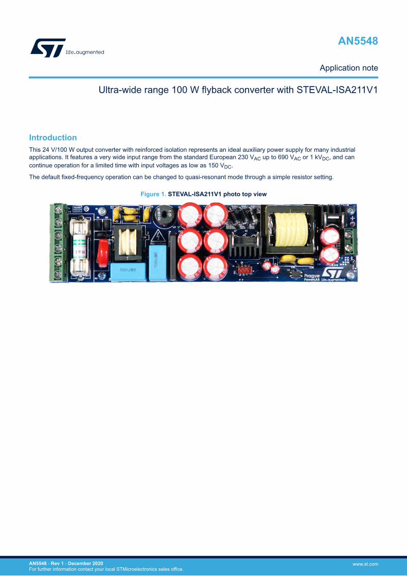
Introduction This 24 V/100 W output converter with reinforced isolation represents an ideal auxiliary power supply for many industrial applications. It features a very wide input range from the standard European 230 V AC up to 690 V AC or 1 kV DC , and can continue operation for a limited time with input voltages as low as 150 V DC . The default fixed-frequency operation can be changed to quasi-resonant mode through a simple resistor setting. Figure 1. STEVAL-ISA211V1 photo top view Ultra-wide range 100 W flyback converter with STEVAL-ISA211V1 AN5548 Application note AN5548 - Rev 1 - December 2020 For further information contact your local STMicroelectronics sales office. www.st.com
-
Upload
khangminh22 -
Category
Documents
-
view
3 -
download
0
Transcript of Ultra-wide range 100 W flyback converter with STEVAL ...
IntroductionThis 24 V/100 W output converter with reinforced isolation represents an ideal auxiliary power supply for many industrialapplications. It features a very wide input range from the standard European 230 VAC up to 690 VAC or 1 kVDC, and cancontinue operation for a limited time with input voltages as low as 150 VDC.
The default fixed-frequency operation can be changed to quasi-resonant mode through a simple resistor setting.
Figure 1. STEVAL-ISA211V1 photo top view
Ultra-wide range 100 W flyback converter with STEVAL-ISA211V1
AN5548
Application note
AN5548 - Rev 1 - December 2020For further information contact your local STMicroelectronics sales office.
www.st.com

1 Overview
Table 1. STEVAL-ISA211V1 board parameters
Symbol Parameter Test Conditions min typ. max Unit
VIN
Input voltage AC 100W load 230 - 690
VInput voltage DC 100W load 250 - 1000
Input voltage AC 50W load 180 - 690
Input voltage DC 50W load 150 - 1000
VOUTt Output voltage - - 24 - V
POUT Output power Vin 230VAC – 1kVDC 100 - - W
η Efficiency
Vin 230VAC, 100W load - 86.0 -
%Vin 400VAC, 100W load - 88.0 -
Vin 1kVDC, 100W load - 85.9 -
Vin 150VDC, 50W load - 86.2 -
AN5548Overview
AN5548 - Rev 1 page 2/15
2 Design description
The converter is based on the L6566BH multi-mode controller in standard single-switch Flyback topology withisolated output, implementing discontinuous-conduction mode operation for every input voltage.
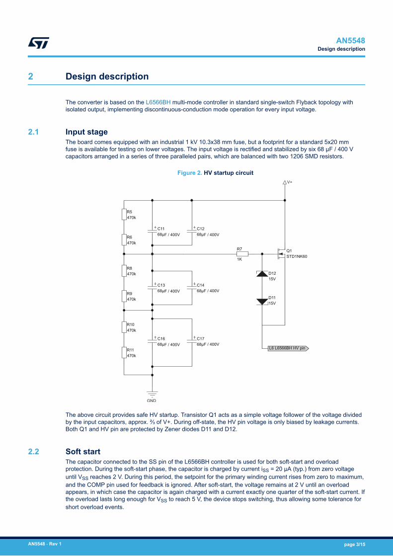
2.1 Input stageThe board comes equipped with an industrial 1 kV 10.3x38 mm fuse, but a footprint for a standard 5x20 mmfuse is available for testing on lower voltages. The input voltage is rectified and stabilized by six 68 μF / 400 Vcapacitors arranged in a series of three paralleled pairs, which are balanced with two 1206 SMD resistors.
Figure 2. HV startup circuit
68μF / 400V
R8
470k
C14
68μF / 400V
470k
R9
470k
C1668μF / 400V
R7
R10
470k
68μF / 400V
D1215V
C17
1K
R11
C12
68μF / 400V
C11
V+
GND
R5
470k
Q1STD1NK60
C1368μF / 400V
R6
470k
D1115V
L6 L6566BH HV pin
The above circuit provides safe HV startup. Transistor Q1 acts as a simple voltage follower of the voltage dividedby the input capacitors, approx. ⅔ of V+. During off-state, the HV pin voltage is only biased by leakage currents.Both Q1 and HV pin are protected by Zener diodes D11 and D12.
2.2 Soft startThe capacitor connected to the SS pin of the L6566BH controller is used for both soft-start and overloadprotection. During the soft-start phase, the capacitor is charged by current iSS = 20 μA (typ.) from zero voltageuntil VSS reaches 2 V. During this period, the setpoint for the primary winding current rises from zero to maximum,and the COMP pin used for feedback is ignored. After soft-start, the voltage remains at 2 V until an overloadappears, in which case the capacitor is again charged with a current exactly one quarter of the soft-start current. Ifthe overload lasts long enough for VSS to reach 5 V, the device stops switching, thus allowing some tolerance forshort overload events.
AN5548Design description
AN5548 - Rev 1 page 3/15
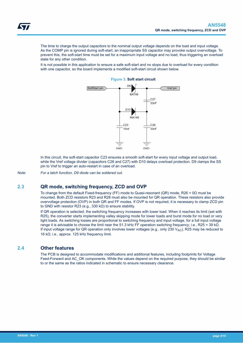
The time to charge the output capacitors to the nominal output voltage depends on the load and input voltage.As the COMP pin is ignored during soft-start, an inappropriate SS capacitor may provoke output overvoltage. Toprevent this, the soft-start time must be set for a maximum input voltage and no load, thus triggering an overloadstate for any other condition.It is not possible in this application to ensure a safe soft-start and no stops due to overload for every conditionwith one capacitor, so the board implements a modified soft-start circuit shown below.
Figure 3. Soft start circuit
10nFC23
33nFC26
GND
D9
BAT48
SoftStart pin
GND
D10
IN4148
33nFC27
Vref pin
In this circuit, the soft-start capacitor C23 ensures a smooth soft-start for every input voltage and output load,while the Vref voltage divider (capacitors C26 and C27) with D10 delays overload protection. D9 clamps the SSpin to Vref to trigger an auto-restart in case of an overload.
Note: For a latch function, D9 diode can be soldered out.
2.3 QR mode, switching frequency, ZCD and OVPTo change from the default Fixed-frequency (FF) mode to Quasi-resonant (QR) mode, R26 = 0Ω must bemounted. Both ZCD resistors R23 and R28 must also be mounted for QR operation. These resistors also provideovervoltage protection (OVP) in both QR and FF modes. If OVP is not required, it is necessary to clamp ZCD pinto GND with resistor R23 (e.g., 330 kΩ) to ensure stability.If QR operation is selected, the switching frequency increases with lower load. When it reaches its limit (set withR25), the converter starts implementing valley skipping mode for lower loads and burst mode for no load or verylight loads. As switching losses are proportional to switching frequency and input voltage, for a full input voltagerange it is advisable to choose the limit near the 51.3 kHz FF operation switching frequency; i.e., R25 = 39 kΩ.If input voltage range for QR operation only involves lower voltages (e.g., only 230 VAC), R25 may be reduced to16 kΩ; i.e., approx. 125 kHz frequency limit.
2.4 Other featuresThe PCB is designed to accommodate modifications and additional features, including footprints for VoltageFeed-Forward and AC_OK components. While the values depend on the required purpose, they should be similarto or the same as the ratios indicated in schematic to ensure necessary clearance.
AN5548QR mode, switching frequency, ZCD and OVP
AN5548 - Rev 1 page 4/15
3 Realized application
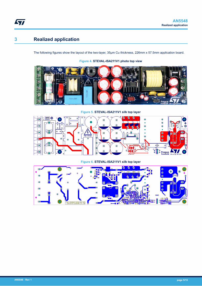
The following figures show the layout of the two-layer, 35µm Cu thickness, 226mm x 57.5mm application board.
Figure 4. STEVAL-ISA211V1 photo top view
Figure 5. STEVAL-ISA211V1 silk top layer
Figure 6. STEVAL-ISA211V1 silk top layer
AN5548Realized application
AN5548 - Rev 1 page 5/15
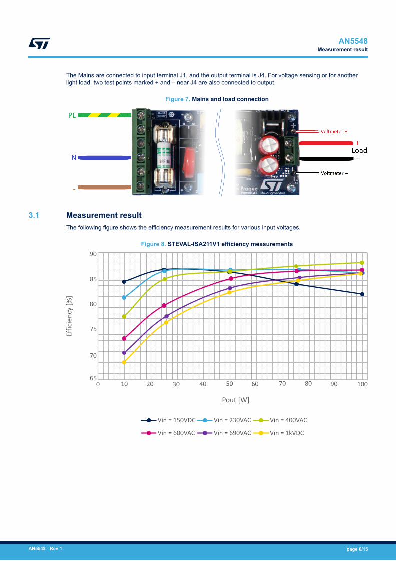
The Mains are connected to input terminal J1, and the output terminal is J4. For voltage sensing or for anotherlight load, two test points marked + and – near J4 are also connected to output.
Figure 7. Mains and load connection
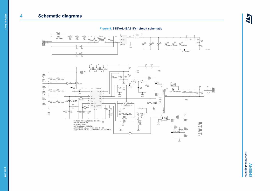
3.1 Measurement resultThe following figure shows the efficiency measurement results for various input voltages.
Figure 8. STEVAL-ISA211V1 efficiency measurements
Effic
ienc
y [%
]
Pout [W]
Vin = 150VDC Vin = 230VAC Vin = 400VAC
Vin = 600VAC Vin = 690VAC Vin = 1kVDC
65
70
75
80
85
90
0 10 20 30 40 50 60 70 80 90 100
AN5548Measurement result
AN5548 - Rev 1 page 6/15
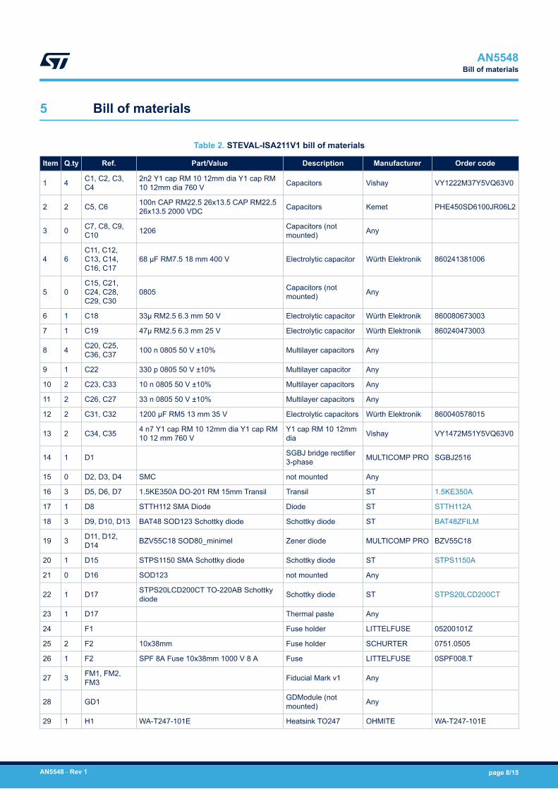
4 Schematic diagrams
Figure 9. STEVAL-ISA211V1 circuit schematic
120kR39
C21
1
1 HV
Q2
GND
C3
GND
GND
C17
100nF
100nC25
C9
470kR5
N/A
1k5
GD1
VREF
ZCD 11
D8
ca100kR18
3
D10
U3TL431_SMD
10R
N/A
1
C15
D2
C32
15V
R4
Vout
1
R27
GND
C36
R2316k / 330k
C23
C35
R38S1
C19
1.5KE350A
D7
GND2
GND
68uF / 400V
15
16AC_OK
U1
68uF / 400VC12
3
D14BAT48
N/A
C5 N/A
_J3
ca1MR16
ca1M
R13
N/A / 0R
47k
1
3
2n2
C1
GND
1
22k
GND
C8
V+
4 GND9
GND2
F1 N/A
DIS
2
14VFF
N/A
R22
GNDC26
4
Q3
1K
C29
H1
33n
Rf
Rg
Rh
470kR8
2n2
1200uF
C11
R30 N/A Vout
D12
D5
470kR10
R25
1200uF
1.5KE350A
2T1
1K
R37
715V
Cc3
1k
R33
S4
10R
D17 STPS20LCD200
R22x3.6mH
COMP
10
GND
1
Optoisolator1
470kR6
15k
D1
SGBJ2516
SS
C22
68uF / 400VC14
NTC
L6566B(H)
C34
ca1M
D13
N/A
R11
10RR1
L2 680uH
U
R12
39k
V+
3
STPS1150
R21
0R
GND
N/A
J4
68uF / 400V
14
8
R32
330m
C27
100nF
Ld
330R
R35
C33
2
Cc1
Ri
2
2n2
C20
D4
4n7
BC817
FMODCS 7
N/A
La V+a
PEa
PEb
Na
Ga
GS
S
Ra
Rb
Rc
Rd
Re
2
C24
N/A
Snubber
NTC
3
470k
J2+
100n
Cc2
Q1
2n2
N/A
68uF / 400VC13 D11
C37
R3
FF: R28 & R26 N/A; R25 39k; R23 330kQR: R26 0R; R25 16k
R7
C18
1
2n2
N/A
100n
GND2
Source
S3
33u
8
1
1k1
N/A
H2
R20330k / N/A
1K
3 IN
ca1MR14
NTCW
PE
J1LN
Input 1.5KE350A
D6
R34
R24
R31 10R
68uF / 400VC16
-
C31
R28
10n
12 Mode/SC
OSC13
330p
33n
C2
4n7
GND
C7L1
GND
5
R17
C10
GND
VCC
6
F2 SPF 8A
STD1NK60
2
R36
R40
D15
0R
N/A
V
GND
3
S2
3G
ND
N/A
BAT48
9k1
470kR9
R26
+
10n
V+
2n2
C30
OCP Latch: D9 N/AOCP AutoRestart: D9 BAT41AC_OK & VFF not used -> R20 330k, R19 0RAC_OK & VFF not used - > R12-18 N/A, C15 & C24 N/A
C28
100n
Le
STTH112
Output
R19
6
C6
18V
U2
4GD
VCC
D16
D3
Gate5
D9BAT48
47u
VAR
C4
Snubber
ca1MR15
2
Lb Lc
G
AN
5548 - Rev 1
page 7/15
AN
5548Schem
atic diagrams
5 Bill of materials
Table 2. STEVAL-ISA211V1 bill of materials
Item Q.ty Ref. Part/Value Description Manufacturer Order code
1 4 C1, C2, C3,C4
2n2 Y1 cap RM 10 12mm dia Y1 cap RM10 12mm dia 760 V Capacitors Vishay VY1222M37Y5VQ63V0
2 2 C5, C6 100n CAP RM22.5 26x13.5 CAP RM22.526x13.5 2000 VDC Capacitors Kemet PHE450SD6100JR06L2
3 0 C7, C8, C9,C10 1206 Capacitors (not
mounted) Any
4 6C11, C12,C13, C14,C16, C17
68 µF RM7.5 18 mm 400 V Electrolytic capacitor Würth Elektronik 860241381006
5 0C15, C21,C24, C28,C29, C30
0805 Capacitors (notmounted) Any
6 1 C18 33µ RM2.5 6.3 mm 50 V Electrolytic capacitor Würth Elektronik 860080673003
7 1 C19 47µ RM2.5 6.3 mm 25 V Electrolytic capacitor Würth Elektronik 860240473003
8 4 C20, C25,C36, C37 100 n 0805 50 V ±10% Multilayer capacitors Any
9 1 C22 330 p 0805 50 V ±10% Multilayer capacitor Any
10 2 C23, C33 10 n 0805 50 V ±10% Multilayer capacitors Any
11 2 C26, C27 33 n 0805 50 V ±10% Multilayer capacitors Any
12 2 C31, C32 1200 µF RM5 13 mm 35 V Electrolytic capacitors Würth Elektronik 860040578015
13 2 C34, C35 4 n7 Y1 cap RM 10 12mm dia Y1 cap RM10 12 mm 760 V
Y1 cap RM 10 12mmdia Vishay VY1472M51Y5VQ63V0
14 1 D1 SGBJ bridge rectifier3-phase MULTICOMP PRO SGBJ2516
15 0 D2, D3, D4 SMC not mounted Any
16 3 D5, D6, D7 1.5KE350A DO-201 RM 15mm Transil Transil ST 1.5KE350A
17 1 D8 STTH112 SMA Diode Diode ST STTH112A
18 3 D9, D10, D13 BAT48 SOD123 Schottky diode Schottky diode ST BAT48ZFILM
19 3 D11, D12,D14 BZV55C18 SOD80_minimel Zener diode MULTICOMP PRO BZV55C18
20 1 D15 STPS1150 SMA Schottky diode Schottky diode ST STPS1150A
21 0 D16 SOD123 not mounted Any
22 1 D17 STPS20LCD200CT TO-220AB Schottkydiode Schottky diode ST STPS20LCD200CT
23 1 D17 Thermal paste Any
24 F1 Fuse holder LITTELFUSE 05200101Z
25 2 F2 10x38mm Fuse holder SCHURTER 0751.0505
26 1 F2 SPF 8A Fuse 10x38mm 1000 V 8 A Fuse LITTELFUSE 0SPF008.T
27 3 FM1, FM2,FM3 Fiducial Mark v1 Any
28 GD1 GDModule (notmounted) Any
29 1 H1 WA-T247-101E Heatsink TO247 OHMITE WA-T247-101E
AN5548Bill of materials
AN5548 - Rev 1 page 8/15
Item Q.ty Ref. Part/Value Description Manufacturer Order code
30 1 H2 WA-T220-101E Heatsink TO220 OHMITE WA-T220-101E
31 1 J1 3x MC000054 6x Screw 1kV RM 9.52 -3Pin 6x Screw 1kV RM 9.52 - 3Pin
6x Screw 1kV RM9.52 - 3Pin MULTICOMP PRO MC000054
32 2 J2, J3 1.32 mm Test point VERO 20-313145
33 1 J4 RM 9.52 2x Screw 1kV RM 9.52 Jumper MULTICOMP PRO MC000054
34 1 L1 2x3.6mH Coilcraft E35xx CMM Coilcraft E3502-AL
35 1 L2 680µH Ind Coilcraft PCV-2 1.3 A Ind Coilcraft PCV-2 Coilcraft PCV-2-684-01L
36 1 L2 8G206M3X30 Polyamide screw DREMEC 8G206M3X30
37 1 L2 M3/BN81 M3 Polyamide nut BOSSARD M3/BN81
38 2 L2 1404830 M3 Polyamide pad BOSSARD 1404830
39 1 Q1 STD1NK60T4 D pak MOSFET MOSFET ST STD1NK60T4
40 1 Q2 BC817-40 SOT23 Signal BJT Any
41 1 Q3 SMICA-SOT93-2 Isolation pad NINIGI SMICA SOT93-2
42 1 Q3 STW12N170K5 TO-247 Power MOSFET ST STW12N170K5
43 3 R1, R2, R3 10R NTC RM5 dia 8.5 NTC RM5 dia 8.5 Resistors EPCOS B57153S0100M000
44 1 R4 V1000LA160BP Var RM8.5 dia 20V1000LA Varistor Varistor LITTELFUSE V1000LA160BP
45 6 R5, R6, R8,R9, R10, R11 470k 1206 Resistor 0.25 W 1% Resistors Any
46 1 R7 1K 1206 Resistor 0.25 W 1% Resistor Any
47 R12, R24,R27, R30 0805 Resistors (not
mounted) Any
48
R13, R14,R15, R16,R17, R18,R28
1206 Resistors (notmounted) Any
49 1 R19 0 R 0805 0.125 W ±1% Resistor Any
50 2 R20, R23 330 k 0805 0.125 W ±1% Resistor Any
51 2 R21, R32 0R 1206 0.25 W ±1% Resistor Any
52 1 R22 1k5 0805 0.125 W ±1% Resistor Any
53 1 R25 39k 0805 0.125 W ±1% Resistor Any
54 R26 0805 Resistor (notmounted) Any
55 1 R31 10 R 0805 Resistor 0.125 W ±1% Resistor Any
56 1 R33 330 m 2512 1 W ±1% Current SenseResistor Any
57 1 R34 1 k 0805 0.125 W ±1% Resistor Any
58 1 R35 330 R 0805 0.125 W ±1% Resistor Any
59 1 R36 9k1 0805 Resistor 0.125 W ±1% Resistor Any
60 1 R37 1k1 0805 Resistor 0.125 W ±1% Resistor Any
61 1 R38 22k 0805 Resistor 0.125 W ±1% Resistor Any
62 1 R39 120k 0805 Resistor 0.125 W ±1% Resistor Any
63 1 R40 15k 0805 Resistor 0.125 W ±1% Resistor Any
64 4 S1, S2, S3,S4 M3 10 mm Spacer stud Würth Elektronik 970100351
AN5548Bill of materials
AN5548 - Rev 1 page 9/15

Item Q.ty Ref. Part/Value Description Manufacturer Order code
65 4 S1, S2, S3,S4 Screw M3 Bossard 1006614
66 1 T1 Custom transformer Würth Elektronik 750318247
67 1 U1 L6566BH SOIC16 PWM controller PWM controller ST L6566BH
68 1 U2 HCPL-817-00DE PDIP4 Optoisolator Optoisolator Broadcom / Avago HCPL-817-00DE
69 1 U3 TL431AIL3T SOT23 LP Voltage reference Voltage reference ST TL431AIL3T
AN5548Bill of materials
AN5548 - Rev 1 page 10/15

Revision history
Table 3. Document revision history
Date Version Changes
11-Dec-2020 1 Initial release.
AN5548
AN5548 - Rev 1 page 11/15
Contents
1 Overview . . . . . . . . . . . . . . . . . . . . . . . . . . . . . . . . . . . . . . . . . . . . . . . . . . . . . . . . . . . . . . . . . . . . . . . . . .2
2 Design description . . . . . . . . . . . . . . . . . . . . . . . . . . . . . . . . . . . . . . . . . . . . . . . . . . . . . . . . . . . . . . . .3
2.1 Input stage . . . . . . . . . . . . . . . . . . . . . . . . . . . . . . . . . . . . . . . . . . . . . . . . . . . . . . . . . . . . . . . . . . . . 3
2.2 Soft start . . . . . . . . . . . . . . . . . . . . . . . . . . . . . . . . . . . . . . . . . . . . . . . . . . . . . . . . . . . . . . . . . . . . . . 3
2.3 QR mode, switching frequency, ZCD and OVP. . . . . . . . . . . . . . . . . . . . . . . . . . . . . . . . . . . . . . 4
2.4 Other features . . . . . . . . . . . . . . . . . . . . . . . . . . . . . . . . . . . . . . . . . . . . . . . . . . . . . . . . . . . . . . . . . 4
3 Realized application . . . . . . . . . . . . . . . . . . . . . . . . . . . . . . . . . . . . . . . . . . . . . . . . . . . . . . . . . . . . . . .5
3.1 Measurement result . . . . . . . . . . . . . . . . . . . . . . . . . . . . . . . . . . . . . . . . . . . . . . . . . . . . . . . . . . . . 6
4 Schematic diagrams . . . . . . . . . . . . . . . . . . . . . . . . . . . . . . . . . . . . . . . . . . . . . . . . . . . . . . . . . . . . . . .7
5 Bill of materials . . . . . . . . . . . . . . . . . . . . . . . . . . . . . . . . . . . . . . . . . . . . . . . . . . . . . . . . . . . . . . . . . . . .8
Revision history . . . . . . . . . . . . . . . . . . . . . . . . . . . . . . . . . . . . . . . . . . . . . . . . . . . . . . . . . . . . . . . . . . . . . . .11
AN5548Contents
AN5548 - Rev 1 page 12/15
List of figuresFigure 1. STEVAL-ISA211V1 photo top view . . . . . . . . . . . . . . . . . . . . . . . . . . . . . . . . . . . . . . . . . . . . . . . . . . . . . . 1Figure 2. HV startup circuit . . . . . . . . . . . . . . . . . . . . . . . . . . . . . . . . . . . . . . . . . . . . . . . . . . . . . . . . . . . . . . . . . . 3Figure 3. Soft start circuit. . . . . . . . . . . . . . . . . . . . . . . . . . . . . . . . . . . . . . . . . . . . . . . . . . . . . . . . . . . . . . . . . . . . 4Figure 4. STEVAL-ISA211V1 photo top view . . . . . . . . . . . . . . . . . . . . . . . . . . . . . . . . . . . . . . . . . . . . . . . . . . . . . . 5Figure 5. STEVAL-ISA211V1 silk top layer . . . . . . . . . . . . . . . . . . . . . . . . . . . . . . . . . . . . . . . . . . . . . . . . . . . . . . . . 5Figure 6. STEVAL-ISA211V1 silk top layer . . . . . . . . . . . . . . . . . . . . . . . . . . . . . . . . . . . . . . . . . . . . . . . . . . . . . . . . 5Figure 7. Mains and load connection. . . . . . . . . . . . . . . . . . . . . . . . . . . . . . . . . . . . . . . . . . . . . . . . . . . . . . . . . . . . 6Figure 8. STEVAL-ISA211V1 efficiency measurements . . . . . . . . . . . . . . . . . . . . . . . . . . . . . . . . . . . . . . . . . . . . . . . 6Figure 9. STEVAL-ISA211V1 circuit schematic . . . . . . . . . . . . . . . . . . . . . . . . . . . . . . . . . . . . . . . . . . . . . . . . . . . . . 7
AN5548List of figures
AN5548 - Rev 1 page 13/15

List of tablesTable 1. STEVAL-ISA211V1 board parameters . . . . . . . . . . . . . . . . . . . . . . . . . . . . . . . . . . . . . . . . . . . . . . . . . . . . . 2Table 2. STEVAL-ISA211V1 bill of materials . . . . . . . . . . . . . . . . . . . . . . . . . . . . . . . . . . . . . . . . . . . . . . . . . . . . . . . 8Table 3. Document revision history . . . . . . . . . . . . . . . . . . . . . . . . . . . . . . . . . . . . . . . . . . . . . . . . . . . . . . . . . . . . . 11
AN5548List of tables
AN5548 - Rev 1 page 14/15

IMPORTANT NOTICE – PLEASE READ CAREFULLY
STMicroelectronics NV and its subsidiaries (“ST”) reserve the right to make changes, corrections, enhancements, modifications, and improvements to STproducts and/or to this document at any time without notice. Purchasers should obtain the latest relevant information on ST products before placing orders. STproducts are sold pursuant to ST’s terms and conditions of sale in place at the time of order acknowledgement.
Purchasers are solely responsible for the choice, selection, and use of ST products and ST assumes no liability for application assistance or the design ofPurchasers’ products.
No license, express or implied, to any intellectual property right is granted by ST herein.
Resale of ST products with provisions different from the information set forth herein shall void any warranty granted by ST for such product.
ST and the ST logo are trademarks of ST. For additional information about ST trademarks, please refer to www.st.com/trademarks. All other product or servicenames are the property of their respective owners.
Information in this document supersedes and replaces information previously supplied in any prior versions of this document.
© 2020 STMicroelectronics – All rights reserved
AN5548
AN5548 - Rev 1 page 15/15