
Analysis, Design and Development of a Single Switch Flyback ...
10
318 Journal of Power Electronics, Vol. 7, No. 4, October 2007 JPE 7-4-7 Analysis, Design and Development of a Single Switch Flyback Buck-Boost AC-DC Converter for Low Power Battery Charging Applications Bhim Singh * and Ganesh Dutt Chaturvedi † †* Dept. of Electrical Engineering, Indian Institute of Technology, New Delhi, India ABSTRACT The design and performance analysis of a power factor corrected (PFC), single-phase, single switch flyback buck-boost ac-dc converter is carried out for low power battery charging applications. The proposed configuration of the flyback buck-boost ac-dc converter consists of only one switch and operates in discontinuous current mode (DCM), resulting in simplicity in design and manufacturing and reduction in input current total harmonic distortion (THD). The design procedure of the flyback buck-boost ac-dc converter is presented for the battery charging application. To verify and investigate the design and performance, a simulation study of the flyback buck-boost converter in DCM is performed using the PSIM6.0 platform. A laboratory prototype of the proposed single switch flyback buck-boost ac-dc converter is developed and test results are presented to validate the design and developed model of the system. Keywords: Single switch flyback converter, Power quality improvement, THD, Power factor 1. Introduction The power electronic equipment connected to an electricity distribution network usually needs some kind of power conditioning, typically rectification, which draws a nonsinusoidal line current due to the nonlinear input characteristic. With the steadily increasing use of such equipment (e.g. TVs, office equipment, battery chargers, electronic ballasts, household appliances, etc.) line current harmonics, power factor, low efficiency and output voltage ripple have become significant problems in these applications. There is a need in the input stage for a reduction in line current harmonics, power factor correction (PFC), efficiency improvement and reduction in output voltage ripple. In recent years, many new alternatives for AC-DC conversion have been proposed which result in reduction of the harmonic distortion and the improvement of power factor [1] . Various international agencies have created standards such as IEEE-519 [2] and IEC 61000-3-2 [3] which impose strict limitations on the levels of harmonic current emissions. These standards have led to continuous research into different methods and approaches for reducing these harmonic currents and improving the power quality indices. This paper presents a topology of a fourth order single switch buck-boost converter with minimal components. For low power applications, DCM (discontinuous conduction mode) operation of the flyback buck-boost Manuscript received April 23, 2007; revised August 31, 2007 † Corresponding Author: [email protected] Tel: +91-23344519 * Dept. of Electrical Engineering, IIT Delhi, New Delhi, India
-
Upload
khangminh22 -
Category
Documents
-
view
2 -
download
0
Transcript of Analysis, Design and Development of a Single Switch Flyback ...
318 Journal of Power Electronics, Vol. 7, No. 4, October 2007
JPE 7-4-7
Analysis, Design and Development of a Single Switch Flyback Buck-Boost
AC-DC Converter for Low Power Battery Charging Applications
Bhim Singh* and Ganesh Dutt Chaturvedi†
†*Dept. of Electrical Engineering, Indian Institute of Technology, New Delhi, India
ABSTRACT
The design and performance analysis of a power factor corrected (PFC), single-phase, single switch flyback buck-boost ac-dc converter is carried out for low power battery charging applications. The proposed configuration of the flyback buck-boost ac-dc converter consists of only one switch and operates in discontinuous current mode (DCM), resulting in simplicity in design and manufacturing and reduction in input current total harmonic distortion (THD). The design procedure of the flyback buck-boost ac-dc converter is presented for the battery charging application. To verify and investigate the design and performance, a simulation study of the flyback buck-boost converter in DCM is performed using the PSIM6.0 platform. A laboratory prototype of the proposed single switch flyback buck-boost ac-dc converter is developed and test results are presented to validate the design and developed model of the system.
Keywords: Single switch flyback converter, Power quality improvement, THD, Power factor
1. Introduction The power electronic equipment connected to an electricity distribution network usually needs some kind of power conditioning, typically rectification, which draws a nonsinusoidal line current due to the nonlinear input characteristic. With the steadily increasing use of such equipment (e.g. TVs, office equipment, battery chargers, electronic ballasts, household appliances, etc.) line current harmonics, power factor, low efficiency and output voltage ripple have become significant problems in these applications. There is a need in the input stage for a
reduction in line current harmonics, power factor correction (PFC), efficiency improvement and reduction in output voltage ripple. In recent years, many new alternatives for AC-DC conversion have been proposed which result in reduction of the harmonic distortion and the improvement of power factor [1]. Various international agencies have created standards such as IEEE-519 [2] and IEC 61000-3-2 [3] which impose strict limitations on the levels of harmonic current emissions. These standards have led to continuous research into different methods and approaches for reducing these harmonic currents and improving the power quality indices.
This paper presents a topology of a fourth order single switch buck-boost converter with minimal components. For low power applications, DCM (discontinuous conduction mode) operation of the flyback buck-boost
Manuscript received April 23, 2007; revised August 31, 2007 †Corresponding Author: [email protected] Tel: +91-23344519 *Dept. of Electrical Engineering, IIT Delhi, New Delhi, India
Analysis, Design and Development of a Single Switch Flyback Buck-Boost … 319
converter topology is considered most suitable because the voltage follower approach is applied for the PWM control of the converter. It uses a simple control scheme, which only requires sensing of output voltage. The output voltage regulation is provided by the feedback loop where the output voltage is compared with a reference value and the error is amplified in a PI (proportional integral) controller, which is compared with a saw-tooth ramp, thus providing the pulses to the power switch. This topology has an inherent power factor correction feature with constant duty ratio and switching frequency, offering an attractive solution for low power applications [4].
For high power applications, continuous conduction mode (CCM) operation, which causes less voltage stress on switching devices, is considered most suitable. The conceptual circuit diagram of a single switch AC-DC converter circuit in CCM operation with an average current mode control includes an inner current loop and an outer voltage loop. In the current loop, the input inductor current or capacitor voltage is detected, compared to a reference value and then processed by a suitable current error amplifier. The current error amplifier output is compared with the fixed ramp to generate a proper driving signal for the switch. The outer voltage loop provides the proper current reference signal by multiplying a scaled replica of rectified voltage by the output of the voltage error amplifier, thus providing the pulses to the power switch [5]. The use of only one switch and the relatively simple control circuit required are strong reasons for their choice [6].
The conventional single switch flyback buck-boost converter is generally available for more than 35W rating for fluorescent lamp applications with THD less than 10%. This paper deals with the design of this AC-DC converter in detail and the experimental results confirm that this AC-DC converter can reduce THD to less than 5% to achieve sufficient suppression of output voltage ripple for less than 25W output power. The simulation is carried out using the PSIM6.0 platform for different load conditions of 20%, 50% and 100% of rated power. These results show the fast response of the PI (proportional integral) controller, where the output voltage is regulated to 24V after sudden application and removal of the load. The flyback buck-boost converter is implemented for constant
voltage battery charging applications with inherent power factor correction (PFC) and high frequency transformer isolation. The hardware implementation for the flyback buck-boost converter in DCM operation is carried out using the parameters designed and verified by the simulation results. The flyback buck-boost converter prototype in DCM is tested under different load conditions with a wide range of input voltage to demonstrate the improved steady state performance. The components are selected with closest specifications available in market, and the experimental results show that satisfactory performance is obtained.
2. Circuit and Operation
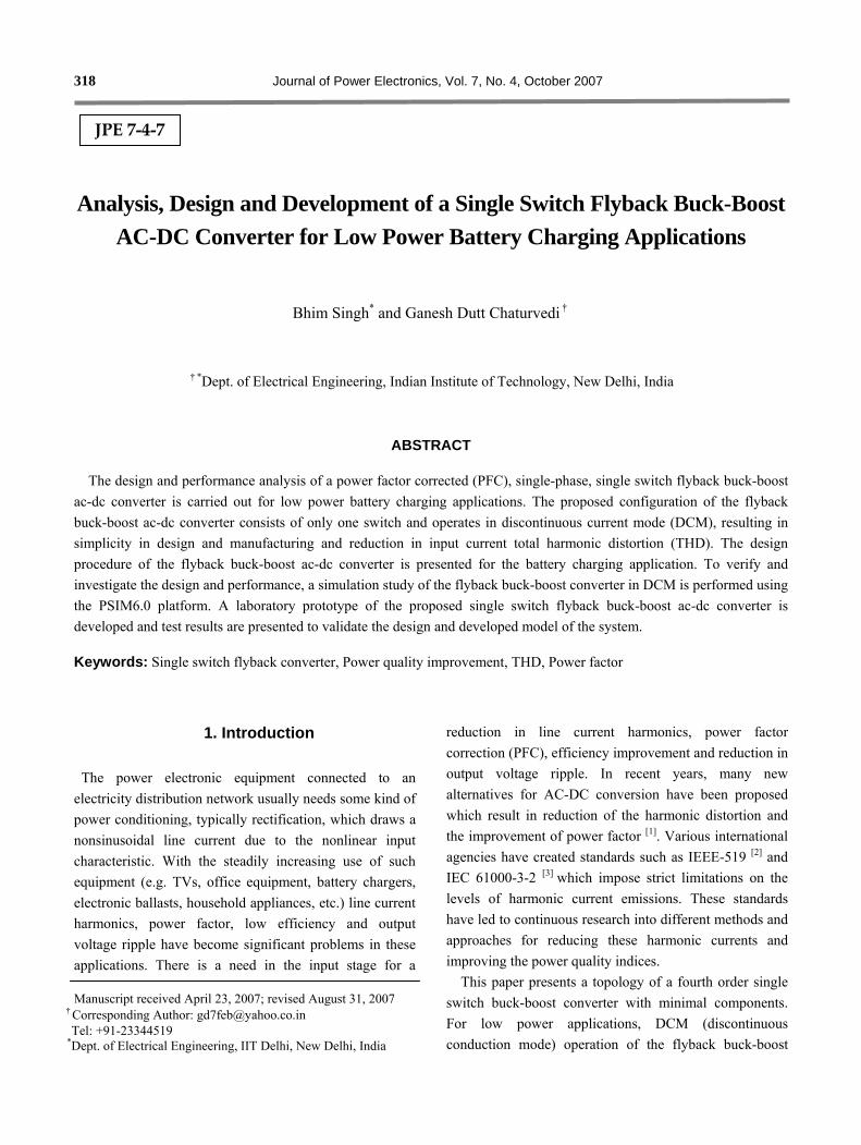
Fig. 1 shows the proposed single-phase, single switch flyback buck-boost converter in DCM operation. This converter consists of the AC power source Vin, input EMI filter of inductor Lf and capacitor Cf, bridge rectifier FWR, high frequency transformer with primary windings N1 and secondary windings N2, high frequency diodes D1, and capacitor Co.
Fig. 1 Practical single-phase, single switch flyback buck-boost converter
The input filter is required to reduce the ripple in the
input current and power factor correction. A large value of the input capacitor distorts the input current waveform as the input current becomes discontinuous due to the fact that the reactive energy of capacitor fC can not be fed back to the input supply in the presence of the diode bridge. Thus, a small value should be selected for the input filter capacitor. Practical flyback converter operation is fundamentally different from other topologies in which energy is stored in the transformer when the switch is on and the power is delivered to the load when the switch is
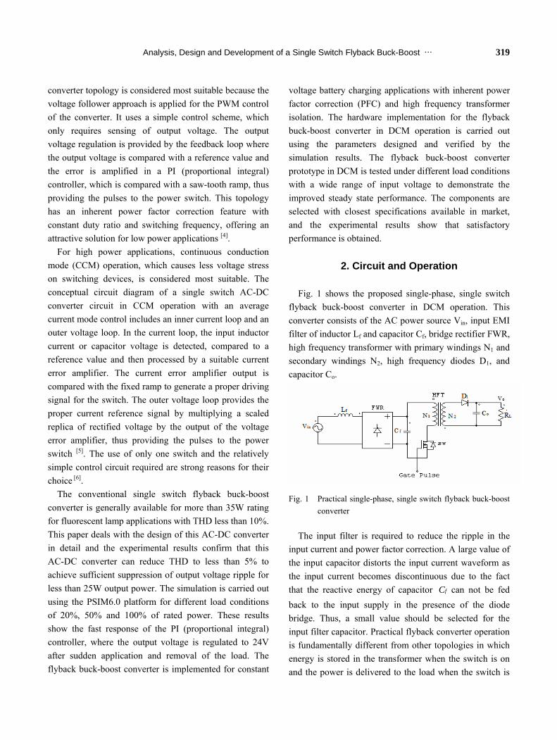
320 Journal of Power Electronics, Vol. 7, No. 4, October 2007 off. In discontinuous conduction mode, the voltage follower approach is applied to the PWM control of the converter, which only requires output voltage detection. The output voltage regulation is provided by the feedback loop as shown in Fig.2, where the output voltage detected Vo is compared with a reference value Voref and the error is amplified in a proportional integral (PI) controller which is compared with a saw-tooth ramp Vs, thus providing the pulse to the power switch. Therefore, this circuit is controlled by the change of the on-time interval and constant switching frequency fs.
Fig. 2 Practical voltage follower approach circuit for PWM control
3. Design of the Flyback Buck-Boost Converter
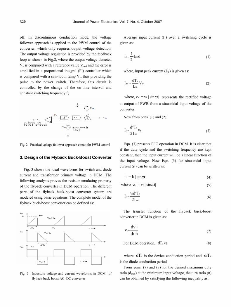
Fig. 3 shows the ideal waveforms for switch and diode
current and transformer primary voltage in DCM. The following analysis proves the resistor emulating property of the flyback converter in DCM operation. The different parts of the flyback buck-boost converter system are modeled using basic equations. The complete model of the flyback buck-boost converter can be defined as:
Fig. 3 Inductors voltage and current waveforms in DCM of flyback buck-boost AC–DC converter
Average input current (I1) over a switching cycle is given as:
1 pk1I I d2
= (1)
where, input peak current (Ipk) is given as:
spk lr
m
dTI VL
= (2)
lr 1where, v = v | sin t|ω represents the rectified voltage
at output of FWR from a sinusoidal input voltage of the converter.
Now from eqns. (1) and (2):
2s
1 lrm
d TI v2L
= (3)
Eqn. (3) presents PFC operation in DCM. It is clear that if the duty cycle and the switching frequency are kept constant, then the input current will be a linear function of the input voltage. Now Eqn. (3) for sinusoidal input current (i1) can be written as:
1 1i = I | sin t| ω (4)
lr 1where, v = v | sin t|ω (5) 2
1 s1
m
v d TI2L
= (6)
The transfer function of the flyback buck-boost converter in DCM is given as:
1r
o=1
dvvd n (7)
For DCM operation, sdT <1 (8)
where sdT is the device conduction period and 1 sd T is the diode conduction period
From eqns. (7) and (8) for the desired maximum duty ratio (dmax) at the minimum input voltage, the turn ratio (n) can be obtained by satisfying the following inequality as:
Analysis, Design and Development of a Single Switch Flyback Buck-Boost … 321
( )1
max o
dn1 d
vv
>− (9)
However, it also affects the voltage stress across the
switch. Thus, a compromise is made between dmax and the voltage stress across the switch to get the turn ratio. The transformer magnetizing inductance is an important factor in deciding the mode of operation. In the flyback converter, it plays the role of a coupled inductor. There are two main criteria used to decide the magnetizing inductance of the transformer. The first one is to select the inductance in order to ensure DCM operation under maximum load conditions. The second criteria depends upon the maximum ripple allowed in the primary current. In order to ensure DCM of operation at maximum load, the following condition must be satisfied:
L min
m 2o
s1 min
RL1 V4fn V
<⎛ ⎞−⎜ ⎟⎝ ⎠
(10)
where mL is the critical inductance, sf is the switching
frequency, L minR is the minimum load resistance and 1 minV is the minimum input voltage of the converter. The output capacitor is selected on the basis of the
maximum peak-to-peak ripple (rv) in output voltage ( oV ) as:
oo
v L
VCw r R
> (11)
The input filter is required to reduce the ripple in the
input current. A large value of the input capacitor distorts the input current waveform as the current becomes discontinuous due to the fact that the reactive energy of capacitor Cf can not be fed back to the input supply in the presence of a one-dimensional diode bridge. Thus, a small value should be selected for the input filter capacitor.
The peak current through switch ( swpkI ) is given as:
L sswpk
m
R dTIL
= (12)
Peak voltage across switch ( swpkV ) given as:
swpk 1 oV V nV= + (13) Similarly, peak current through diode ( dpkI ) is as:
2o 1 s
dpkm
n V d TI
L= (14)
And, peak voltage across the diode ( dpkV ) can be given
as:
1dpk o
VV Vn
= + (15) The switch current at half of the ripple swI∆ is given
as:
1min max ssw
m
V d TIL
∆ = (16)
Switch RMS current ( swrmsI ) is given as:
2 2swrms max sw swpkswpk sw
1I d I I I I3
⎡ ⎤⎛ ⎞= −∆ + ∆⎜ ⎟⎢ ⎥⎝ ⎠⎣ ⎦ (17)
Similarly diode current at half of the ripple ( dhI ) is
given as:
( )0 max
dhmax
II1 d
=− (18)
where, 0 maxI is the maximum output voltage of the
converter. The diode peak current ( dpkI ) for ripple ∆Id is given as:
ddpk dh
II I2
∆= + (19)
where, ( )o max s
d2
V 1 d TI
L−
∆ = (20)
Diode RMS current ( drmsI ) is given as:
( ) 2 2drms max d dpkdpk d
1I 1 d I I I I3
⎡ ⎤⎛ ⎞= − −∆ + ∆⎜ ⎟⎢ ⎥⎝ ⎠⎣ ⎦ (21)
322 Journal of Power Electronics, Vol. 7, No. 4, October 2007
These equations are used to get design data, which are used in the model of the proposed flyback buck-boost converter in PSIM6.0 to analyze the steady state and dynamic behavior of the converter. The simulation is carried out for different load conditions of 20%, 50% and 100% of rated power. The design procedure is presented here for DCM mode of operation for the specifications given in Table I. Based on the above design equations the experimental data is summarized in Table II.
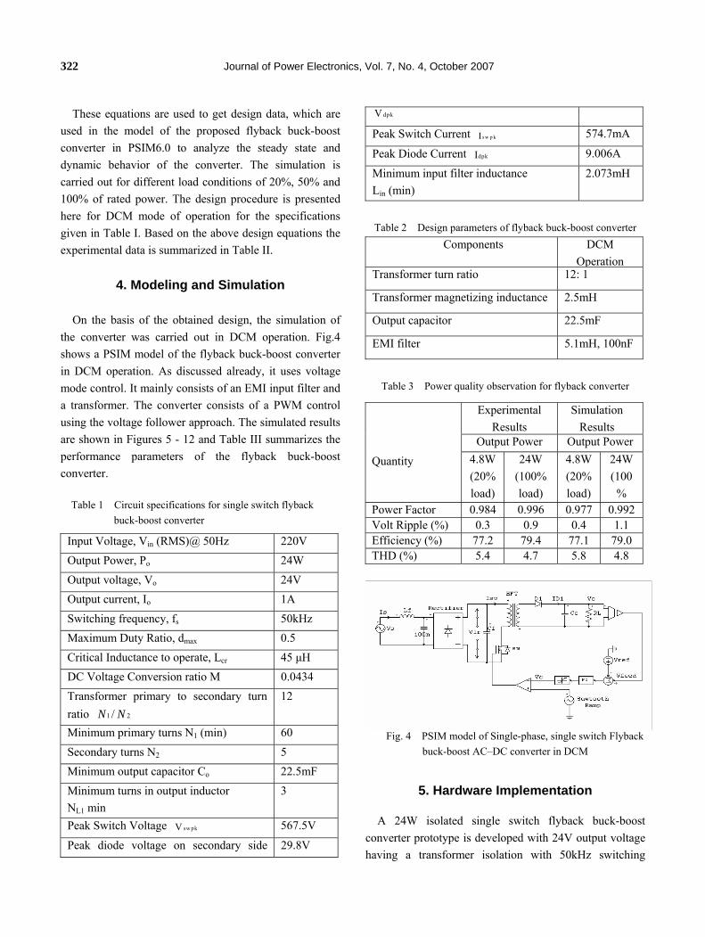
4. Modeling and Simulation
On the basis of the obtained design, the simulation of the converter was carried out in DCM operation. Fig.4 shows a PSIM model of the flyback buck-boost converter in DCM operation. As discussed already, it uses voltage mode control. It mainly consists of an EMI input filter and a transformer. The converter consists of a PWM control using the voltage follower approach. The simulated results are shown in Figures 5 - 12 and Table III summarizes the performance parameters of the flyback buck-boost converter.
Table 1 Circuit specifications for single switch flyback
buck-boost converter
Input Voltage, Vin (RMS)@ 50Hz 220V Output Power, Po 24W Output voltage, Vo 24V Output current, Io 1A Switching frequency, fs 50kHz Maximum Duty Ratio, dmax 0.5 Critical Inductance to operate, Lcr 45 µH DC Voltage Conversion ratio M 0.0434 Transformer primary to secondary turn ratio 1 2/N N
12
Minimum primary turns N1 (min) 60 Secondary turns N2 5 Minimum output capacitor Co 22.5mF Minimum turns in output inductor NL1 min
3
Peak Switch Voltage sw pkV 567.5V
Peak diode voltage on secondary side 29.8V
dpkV
Peak Switch Current s w p kI 574.7mA
Peak Diode Current dpkI 9.006A
Minimum input filter inductance Lin (min)
2.073mH
Table 2 Design parameters of flyback buck-boost converter Components DCM
OperationTransformer turn ratio 12: 1
Transformer magnetizing inductance 2.5mH
Output capacitor 22.5mF
EMI filter 5.1mH, 100nF
Table 3 Power quality observation for flyback converter
Experimental Results
Simulation Results
Output Power Output Power
Quantity 4.8W
(20% load)
24W (100% load)
4.8W(20% load)
24W (100%
Power Factor 0.984 0.996 0.977 0.992Volt Ripple (%) 0.3 0.9 0.4 1.1 Efficiency (%) 77.2 79.4 77.1 79.0 THD (%) 5.4 4.7 5.8 4.8
Fig. 4 PSIM model of Single-phase, single switch Flyback buck-boost AC–DC converter in DCM
5. Hardware Implementation
A 24W isolated single switch flyback buck-boost converter prototype is developed with 24V output voltage having a transformer isolation with 50kHz switching
Analysis, Design and Development of a Single Switch Flyback Buck-Boost … 323
frequency and PFC in DCM operation. It includes the control supply and protection such as overload shutdown, input under voltage and output over voltage. The voltage follower approach is applied to the control using PWM controller chip UC3843. The hardware implementation is carried out using the parameters designed and verified through the simulation results. The photograph of the experimental setup of the flyback buck-boost converter is shown in Fig. 13. Extensive tests were conducted on the developed prototype of the converter and the test results are shown in Figs. 14-20. High input power quality is achieved with improved power factor and reduced source current distortion at full load. The controller shows a fast dynamic response to line and load disturbance with an output voltage ripple of 1% for 4.8W to 24W load changes.
These results show the suitability of DCM operation in low power applications. Table III summarized the power quality observation via comparison between experimental and simulation results of the flyback buck-boost converter. The components used in the hardware implementation of flyback buck-boost converter are summarized in Table IV with a detailed description.
Table 4 Specifications of components used in hardware
implementation of flyback buck-boost converter
Component Company Description Rectifier Diode
General Semiconductor
1N5408 (Vrrm=1000V, If(max)=1A)
MOSFET International
Rectifier 2SK962(N Channel, VDSS=900V, Id=3A)
High Frequency Diode
On Semiconductor
MBR2045CT (Vrrm=45V, If(max)=20A)
Transformer EPCOS EE25 (Ferrite Core), Material-N67
Input Inductor
EPCOS EE20 (Ferrite Core), Material-N67
PWM Controller Chip
Unitrode UC3843
Optocoupler Isolation Chip
Fairchild semiconductor
4N35
6. Result and Discussion
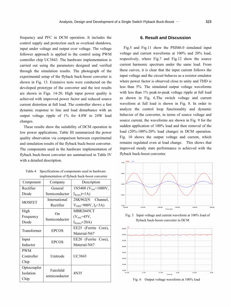
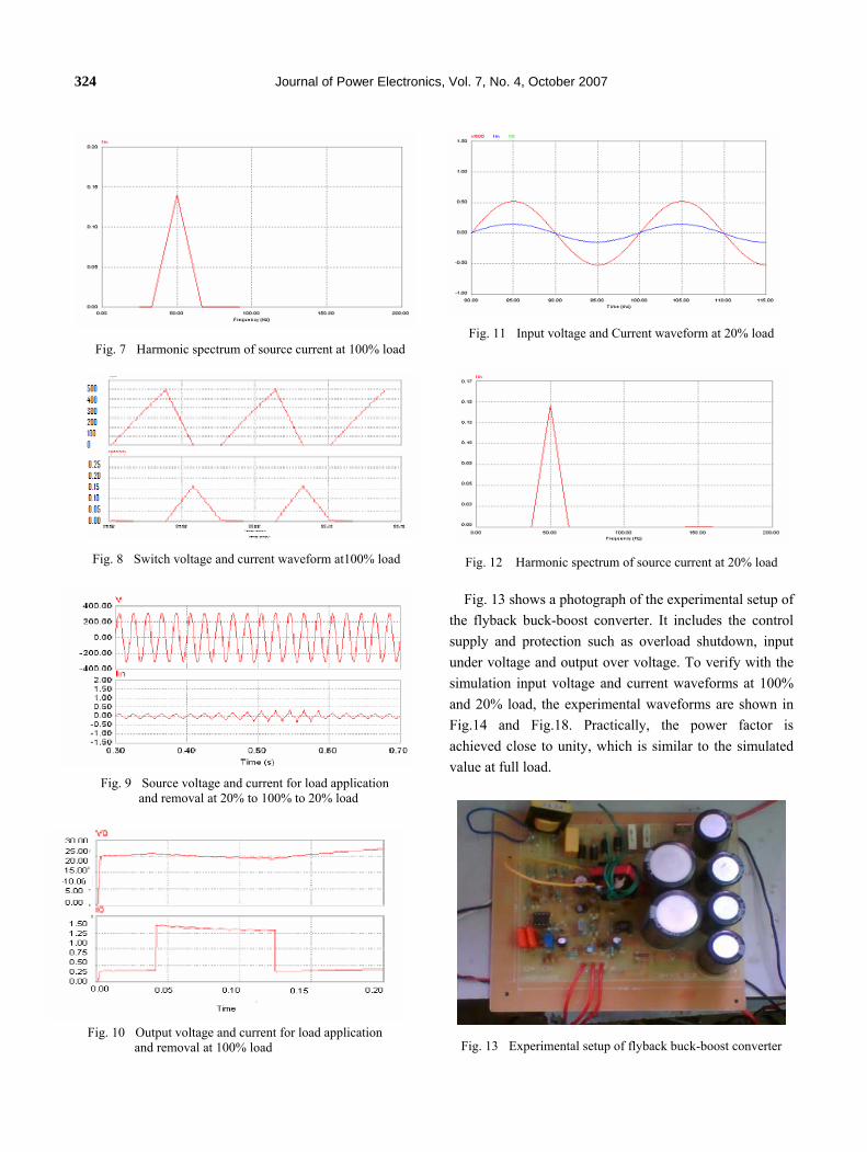
Fig.5 and Fig.11 show the PSIM6.0 simulated input voltage and current waveforms at 100% and 20% load, respectively, where Fig.7 and Fig.12 show the source current harmonic spectrum under the same load. From these curves, it is clear that the input current follows the input voltage and the circuit behaves as a resistor emulator where power factor is observed close to unity and THD is less than 5%. The simulated output voltage waveforms with less than 1% peak-to-peak voltage ripple at full load as shown in Fig. 6.The switch voltage and current waveform at full load is shown in Fig. 8. In order to analyze the control loop functionality and dynamic behavior of the converter, in terms of source voltage and source current, the waveforms are shown in Fig. 9 for the sudden application of 100% load and then removal of the load (20%-100%-20% load change) in DCM operation. Fig. 10 shows the output voltage and current, which remains regulated even at load change. This shows that improved steady state performance is achieved with the flyback buck-boost converter.
Fig. 5 Input voltage and current waveform at 100% load of flyback buck-boost converter in DCM
Fig. 6 Output voltage waveform at 100% load
324 Journal of Power Electronics, Vol. 7, No. 4, October 2007
Fig. 7 Harmonic spectrum of source current at 100% load
Fig. 8 Switch voltage and current waveform at100% load
Fig. 9 Source voltage and current for load application
and removal at 20% to 100% to 20% load
Fig. 10 Output voltage and current for load application
and removal at 100% load
Fig. 11 Input voltage and Current waveform at 20% load
Fig. 12 Harmonic spectrum of source current at 20% load
Fig. 13 shows a photograph of the experimental setup of
the flyback buck-boost converter. It includes the control supply and protection such as overload shutdown, input under voltage and output over voltage. To verify with the simulation input voltage and current waveforms at 100% and 20% load, the experimental waveforms are shown in Fig.14 and Fig.18. Practically, the power factor is achieved close to unity, which is similar to the simulated value at full load.
Fig. 13 Experimental setup of flyback buck-boost converter
Analysis, Design and Development of a Single Switch Flyback Buck-Boost … 325
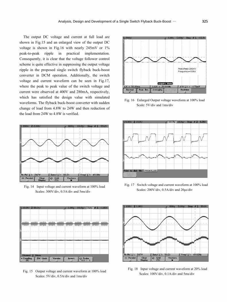
The output DC voltage and current at full load are shown in Fig.15 and an enlarged view of the output DC voltage is shown in Fig.16 with nearly 245mV or 1% peak-to-peak ripple in practical implementation. Consequently, it is clear that the voltage follower control scheme is quite effective in suppressing the output voltage ripple in the proposed single switch flyback buck-boost converter in DCM operation. Additionally, the switch voltage and current waveform can be seen in Fig.17, where the peak to peak value of the switch voltage and current were observed at 400V and 280mA, respectively, which has satisfied the design value with simulated waveforms. The flyback buck-boost converter with sudden change of load from 4.8W to 24W and then reduction of the load from 24W to 4.8W is verified.
Fig. 14 Input voltage and current waveform at 100% load
Scales: 300V/div, 0.5A/div and 5ms/div
Fig. 15 Output voltage and current waveform at 100% load Scales: 5V/div, 0.5A/div and 1ms/div
Fig. 16 Enlarged Output voltage waveform at 100% load
Scale: 5V/div and 1ms/div
Fig. 17 Switch voltage and current waveform at 100% load
Scales: 200V/div, 0.5A/div and 20µs/div
Fig. 18 Input voltage and current waveform at 20% load
Scales: 100V/div, 0.1A/div and 5ms/div
326 Journal of Power Electronics, Vol. 7, No. 4, October 2007
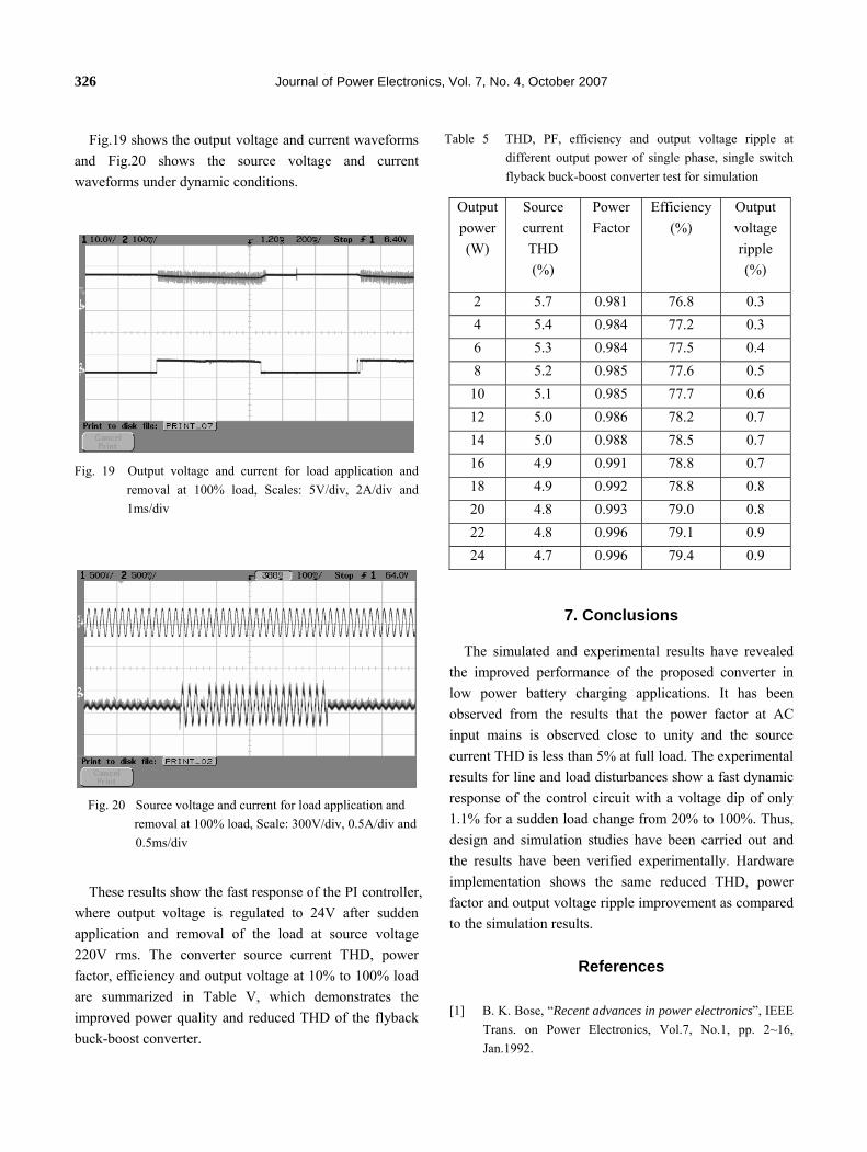
Fig.19 shows the output voltage and current waveforms and Fig.20 shows the source voltage and current waveforms under dynamic conditions.
Fig. 19 Output voltage and current for load application and removal at 100% load, Scales: 5V/div, 2A/div and 1ms/div
Fig. 20 Source voltage and current for load application and
removal at 100% load, Scale: 300V/div, 0.5A/div and 0.5ms/div
These results show the fast response of the PI controller,
where output voltage is regulated to 24V after sudden application and removal of the load at source voltage 220V rms. The converter source current THD, power factor, efficiency and output voltage at 10% to 100% load are summarized in Table V, which demonstrates the improved power quality and reduced THD of the flyback buck-boost converter.
Table 5 THD, PF, efficiency and output voltage ripple at different output power of single phase, single switch flyback buck-boost converter test for simulation
Output power (W)
Source current THD (%)
Power Factor
Efficiency (%)
Output voltage ripple (%)
2 5.7 0.981 76.8 0.3 4 5.4 0.984 77.2 0.3 6 5.3 0.984 77.5 0.4 8 5.2 0.985 77.6 0.5
10 5.1 0.985 77.7 0.6 12 5.0 0.986 78.2 0.7 14 5.0 0.988 78.5 0.7 16 4.9 0.991 78.8 0.7 18 4.9 0.992 78.8 0.8 20 4.8 0.993 79.0 0.8 22 4.8 0.996 79.1 0.9 24 4.7 0.996 79.4 0.9
7. Conclusions
The simulated and experimental results have revealed the improved performance of the proposed converter in low power battery charging applications. It has been observed from the results that the power factor at AC input mains is observed close to unity and the source current THD is less than 5% at full load. The experimental results for line and load disturbances show a fast dynamic response of the control circuit with a voltage dip of only 1.1% for a sudden load change from 20% to 100%. Thus, design and simulation studies have been carried out and the results have been verified experimentally. Hardware implementation shows the same reduced THD, power factor and output voltage ripple improvement as compared to the simulation results.
References [1] B. K. Bose, “Recent advances in power electronics”, IEEE
Trans. on Power Electronics, Vol.7, No.1, pp. 2~16, Jan.1992.

Analysis, Design and Development of a Single Switch Flyback Buck-Boost … 327
[2] IEEE Guide for harmonic control and reactive compensation of Static Power Converters IEEE Standard 519-1992.
[3] Limits for harmonic current emissions, International Electrotechnical Commission Standard 61000-3-2, 2004.
[4] Kin- siu Fung, Wing- Hung Ki and Philip K. T. Mok, “Analysis and Measurement of DCM Power Factor Correctors,” in Proc. IEEE Power Electronics Specialists Conference, 1999, pp.709-714.
[5] S. Buso and G. Spiazzi, “Simplified Control Technique For High-Power Factor Fly Back Cuk And Septic Rectifier Operating In CCM, ” in Proc. of IEEE Conf. on Industry Applications 1999, vol.3, Oct.1999, pp. 1633-1638.
[6] Y. Jiang, and F.C. Lee, “Single-Stage Single-Phase parallel power factor correction scheme,” in Proc. IEEE PESC’94, 1994, pp. 1145-1151.
Bhim Singh (SM’99) was born in Rahamanpur, U.P. India in 1956. He received his B.E. (Electrical) degree from the University of Roorkee, India in 1977 and his M.Tech. and Ph.D. degrees from the Indian Institute of Technology (IIT) , New Delhi, in
1979 and 1983, respectively. In 1983, he joined as a Lecturer and in 1988 became a reader in the department of Electrical Engineering, University of Roorkee. In December 1990, he joined as an assistant Professor, became an Associate Professor in 1994 and full Professor in 1997 in the Department of Electrical Engineering, IIT Delhi. His fields of interest includes power electronics, electrical machines and drives, active filters, static VAR compensators, and analysis and digital control of electrical machines. Prof Singh is a Fellow of the Indian National Academy of Engineering (INAE), Institution of Engineers (India) (IE) (I) and the Institution of Electronics and Telecommunication Engineers (IETE), a life Member of Indian Society for Technical Education (ISTE), System Society of India (SSI) and the national Institution of Quality and Reliability (NIQR) and a Senior Member of IEEE (Institute of Electrical and Electrical and Electronics Engineers).
Ganesh Dutt Chaturvedi was born in Chanderi, M.P. India in 1976. He received his B.E. (Electronics and Communication) degree from R.K.D.F Institute of Science and Technology, Bhopal, India in 1999. In 2000, he joined as a Research Trainee and in 2001
became a Design Engineer in Associated Electronics Research
Foundation, Noida. Presently he is a Research Scholar in the Department of Electrical Engineering, IIT Delhi, pursuing his MS (Research) degree. His fields of interest includes power quality, low power converter design, analog control and microcontroller based digital control.