A High-Efficiency Wide-Input-Voltage Range Switched Capacitor Point-of-Load DC–DC Converter
Upload
independentCategory
view
1download
0
Novel AC-DC andDC-DC Converters with aDiode-Capacitor Multiplier
A. SHENKMAN
Y. BERKOVICH
B. AXELRODHolon Academic Institute of TechnologyIsrael
This paper presents a transformerless ac-dc and or dc-dc
converter with a high output voltage multiplicity, which contains
only one switch. The converter consists of an inverter and a
diode-capacitor multiplier (DCM) and provides a voltage gain
equal to double the number of multiplier steps. In the case of
ac-dc conversion the proposed converter offers a practically
unit power factor and provides a sine wave input current. The
analysis of the steady state as well as the transient behavior of
the DCM is given and simplified equivalent circuits are proposed.
The prototype of the DCM has been built and tested to show the
validity of the proposed converter. The theoretical analysis, the
computer simulation results, and the experimental testing results
are in good agreement.
Manuscript received August 2, 2003; revised March 31, 2004;released for publication August 18, 2004.
IEEE Log No. T-AES/40/4/839854.
Refereeing of this contribution was handled by M. G. Simoes.
Authors’ address: Holon Academic Institute of Technology, Dept.of Electrical and Electronic Engineering, 52 Golomb St., P.O.B. 305Holon, 58102 Israel, E-Mail: ([email protected]).
0018-9251/04/$17.00 c 2004 IEEE
I. INTRODUCTION
Diode-capacitor multipliers (DCMs) (two typicalcircuits are shown in Fig. 1) have been knownfor a long time. These circuits are widely used astransformerless high-voltage multipliers. As is known,such circuits transform the ac voltage in a rectifieddc voltage, which exceeds the amplitude of the inputvoltage in n time (n is the number of capacitors in themultiplier circuit).
Fig. 1. Diode-capacitor ac-dc multipliers. (a) Dickson chargepump. (b) Cookcroft-Walton multiplier.
New interest in these circuits has been recentlycaused by the advent of integrated circuits and thepossibility of replacing the diodes by high frequencyswitches [1, 2]. It enables building the low-powerhigh voltage integrated sources, which do not includeinductive elements and transformers.
Simultaneously in the last few years DCMs havebeen applied in power supplies of a high dc voltagewith a large voltage gain. The source of the ac voltagein these multipliers is the high-frequency voltageinverter. At the same time there were investigationsaimed at simplifying the inverter operation andreducing the number of it switches. One of suchcircuits with one switch and a three-step multiplier hasbeen described in [3]. This circuit provides the voltagegain A= n=2.
This paper deals with a circuit (Fig. 2), in which aone-switch input high-frequency inverter and DCMensures the increase of the input dc voltage in 2ntime, i.e., four times more than in the circuit presentedin [3].
Fig. 2. Schemes of proposed dc-dc (a) and ac-dc (b) multipliers.
The principle of the one-switch inverter operation,which transforms dc or ac input voltage to achigh-frequency intermediate voltage (Fig. 3), isbriefly described. A more detailed activity description
1286 IEEE TRANSACTIONS ON AEROSPACE AND ELECTRONIC SYSTEMS VOL. 40, NO. 4 OCTOBER 2004

Fig. 3. Input ac-ac converter.
Fig. 4. Ideal switching waveforms of input ac-ac converter.
of this inverter is given in [4]. For an ac inputvoltage this inverter ensures a practically unit powerfactor and provides a sine wave input current. TheDCM is nonlinear and therefore its analysis is verycomplicated both in steady state and furthermore intransient operations. The equivalent circuit of DCMs,which consists of only one diode, one capacitor, andone resistor, is offered here. Such an equivalent circuitcan be used for the analysis of the DCMs of anycomplexity. The proposed equivalent circuit is simpleand is evident.
II. SINGLE-SWITCH AC-AC CONVERTER
The scheme of the ac-ac input converter [4] isshown in Fig. 3. The main advantages of this schemeare: on the one hand the high power factor andsine wave input current, and on the other hand theinverter circuit is constructed on a single controlledswitch, which serves as a high-frequency generator forinduction heating.The operating principles of the proposed circuit
can be illustrated by theoretical waveforms, as shownin Fig. 4. We suppose that the switching frequencyis much higher than the input line frequency and inthe analysis we have chosen arbitrary the positivetime interval, i.e., where the input source voltage ispositive: vin, s > 0.1) Interval 1, t0 < t < t1: Four diodes D1r D4r
and the switch SW are OFF. In this interval the
Fig. 5. Circuit diagram of multiplier.
capacitor Cin charges up practically linearly at a rateand a polarity correspondent to the instantaneous inputvoltage vin, s.
2) Interval 2, t1 < t < t2: Two diodes D1r, D3r andthe switch SW are ON. In this interval the capacitorCin is discharging via the circuit: Cin D1r SWLr load C3. This interval ends when the capacitorvoltage reduces to zero.
3) Interval 3, t2 < t < t3: All the diodes and theswitch are ON. In this interval the switch current, i.e.the current through switch SW, flows via two parallelbridge branches. This interval ends when this switchcurrent decreases to zero. At this moment the switchgets off and the process starts from the beginning.
The basic voltage gain of the converter is definedas [4]:
Mg =VoVin, s
= 2
1+R 2o !s
1!s
2
1 cos¼D1D
1:1¼(1 D+D1)
(1)
where !s = !s=!B is the normalized switchingfrequency; !B = 1= LoCo is the base frequency; Ro =Ro=RB is the normalized switching load resistance,RB = Lo=Co is the base resistance, D = (T1 +T2)=T isthe duty cycle of the switch current and D1 = T1=T isthe duty cycle of the capacitor current. Practically, thevoltage gain Mg varies over the range of 1–2.5 with aswitching frequency regulation.
III. OPERATIONAL ANALYSIS OF THEDIODE-CAPACITOR MULTIPLIER
The analysis of the DCM operation is given for thescheme in Fig. 5. Three basic phases of its operationcan be recognized according to 3 basic equivalentcircuits shown in Fig. 6.
The first phase, Fig. 6(a), corresponds to thecondition, where all odd diodes are ON and all theeven diodes are OFF. In this phase, having the timeinterval (#1 #2), see Fig. 9, capacitors C2 C3,C4 C5, etc., that is the capacitors C2k, C2k+1, areseries connected, while capacitor C1 is connecteddirectly to the input voltage and capacitor Cn isconnected directly to the load resistor Rout. As can beseen, the voltages on the series connected capacitorshave opposite polarities and their algebraic sum isequal to the input voltage Vin.
SHENKMAN ET AL.: NOVEL AC-DC AND DC-DC CONVERTERS WITH A DIODE-CAPACITOR MULTIPLIER 1287
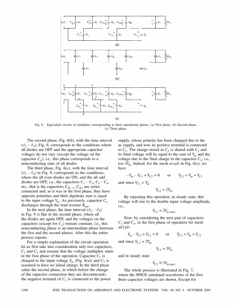
Fig. 6. Equivalent circuits of multiplier corresponding to three operational phases. (a) First phase. (b) Second phase.(c) Third phase.
The second phase, Fig. 6(b), with the time interval(#2 #3), Fig. 9, corresponds to the conditions whereall diodes are OFF and the appropriate capacitorvoltages do not vary (except the voltage on thecapacitor Cn), i.e., this phase corresponds to anonconducting state of all diodes.The third phase, Fig. 6(c), with the time interval
(#3 #4) in Fig. 9, corresponds to the conditions,where the all even diodes are ON, and the all odddiodes are OFF, i.e., the capacitors C1 C2, C3 C4,etc., that is the capacitors C2k 1, C2k, are seriesconnected and, as it was in the first phase, they haveopposite polarities and their algebraic sum is equalto the input voltage Vin. As previously, capacitor Cndischarges through the load resistor Rout.In the next phase, the time interval (#4 #5)
in Fig. 9 is like in the second phase, where allthe diodes are again OFF, and the voltages on thecapacitors (except for Cn) remain constant, i.e., thisnonconducting phase is an intermediate phase betweenthe first and the second phases. After this the entireprocess repeats.For a simple explanation of the circuit operation,
let us first take into consideration only two capacitors,C1 and C2 and assume that the voltage multiplier startsin the first phase of the operation. Capacitor C1 ischarged to the input voltage Vin (Fig. 6(a)) and C2 isassumed to have no initial charge. In the third phase(after the second phase, in which before the changeof the capacitor connection they are disconnected)the negative terminal of C1 is connected to the power
supply, whose polarity has been changed due to theac supply, and now its positive terminal is connectedto C1. The charge stored in C1 is shared with C2 andits final voltage will be equal to the sum of Vin and thevoltage due to the final charge in the capacitor C1, i.e.,too 2Vin. Indeed, for the mesh acegb in Fig. 6(c), wehave
Vin VC1 +VC2 = 0 or VC2 = Vin +VC1
and since VC1 = Vin
VC2 = 2Vin:
By repeating this operation, in steady state, thisvoltage will rise to the double input voltage amplitude,i.e.,
VC2 = 2Vin:max:
Now, by considering the next pair of capacitorsC3 and C4, in the first phase of operation for meshadfgb:
Vin VC3 +VC2 = 0 or VC3 = Vin +VC2
and since VC2 = 2Vin
VC3 = 3Vin
and in steady state
VC3 = 3Vin:max:
The whole process is illustrated in Fig. 7,where the SPICE simulated waveforms of the firstthree-capacitor voltages are shown. Except for
1288 IEEE TRANSACTIONS ON AEROSPACE AND ELECTRONIC SYSTEMS VOL. 40, NO. 4 OCTOBER 2004

Fig. 7. SPICE-simulating switching on process.
Fig. 8. Proposed equivalent ac-circuit.
the capacitor voltages the currents iC through thecapacitors are also shown in Fig. 7.Continuing this analysis by taking into
consideration each time the next pair of capacitors,we may write VC4 = 4Vin:max; VC5 = 5Vin:max; etc,VCk = kVin:max and finally
VCn = Vout = nVin:max: (2)
Referring to the time diagram in Fig. 7, we mayrecognize that during one period of a supply voltagethe voltages on each of the capacitors increase anddecrease, except for the last one, whose voltageincreases all the time. However, the increase ofthe voltages exceeds its decrease and in the steadystate mode these periodic changes become equal. Inpractical circuits the capacitances are large enough,therefore the voltage ripple in steady state is ratherinsignificant. At the same time the differences of thecapacitor voltages VC2k VC2k+1 and VC2k 1
VC2k settledown near to the amplitude of a supply voltage Vin:max,as shown in Fig. 7.For the simplification of the analysis of both the
steady state and the transient behavior of the DCM, itis useful to construct its simplified equivalent circuit.Such a proposed circuit is given in Fig. 8. Let us nowcarry out the comparative analysis of the basic andequivalent circuits.The pair of capacitors C2k, C2k+1 in the first phase
interval (#1 #2) (see Fig. 9) is connected to the input
Fig. 9. Wave-shapes of multiplier input voltage, capacitor current,and sums of two series capacitor voltages.
voltage vin = Vin:max sin!t as shown in Fig. 6(a). Thenthe current through this pair of capacitors will be
iC =C
2dvCdt
=C
2!Vin:max cos!t=
Vin:max2xC
cos!t
oriC = IC:max cos!t #1 #2 (3)
where IC:max = (Vin:max=2xC). The charge transferredvia these two capacitors during half of the period
SHENKMAN ET AL.: NOVEL AC-DC AND DC-DC CONVERTERS WITH A DIODE-CAPACITOR MULTIPLIER 1289

Fig. 10. Input and capacitance voltages and input current inequivalent circuit.
of the supplied voltage can be evaluated as the areaunder the current curve:
¢Q =#2
#1
¢Vin:max2xC
cos!tdt =Vin:max(sin#2 sin#1)
!2xC
=vin(#2) vin(#1)
!2xC=¢Vk:m!2xC
: (4)
In the same way we can evaluate the chargetransferred via the next pair of capacitors C2k 1and C2k during the negative half of period. Sincethe intervals (#1 #2) and (#3 #4) are also equalthe charges transferred are equal. Thus the chargetransferred during the whole period will be
¢Q1 = 2¢Q =¢Vk:m!xC
: (5)
Now let us evaluate the charge transferred in theequivalent circuit (Fig. 8). It can be done with the helpof the input current in the interval #1 #2, shown inFig. 10,
iin =nVin:max sin!t Vo
Req=¢Vr:mReq
sin! t (6)
where ¢Vr:m = nVin:max Vo is the amplitude ofthe equivalent resistor voltage (see Fig. 10). Byintegrating (6) during the interval #1 #2 we obtain
¢Q2 =#2
#1
¢Vr:mReq
sin(! t) dt=¢Vr:m!Req
2cos#2 =¢Vr:eq!Req
:
(7)
Since the input voltage in the equivalent circuit isn times bigger than in the original circuit, it is logicalto conclude that the voltage drop across the resistorin the equivalent circuit is n times bigger than in theoriginal circuit, i.e.,
¢Vr:eq = n¢Vk:m: (8)
By equaling the transferred charges inboth circuits, i.e., ¢Q1 =¢Q2, and taking intoconsideration (8) we have
¢Vk:m!xC
=n¢Vk:m!Req
Fig. 11. Normalized output voltage Vo=nVin:max (a) and relativetime constant ¿=TS (b) versus resistance ratio Req=Rout and circuit
parameter !RourCeq.
which gives
Req = nxC =n
!C: (9)
Finally, since in the original circuit the charge istransferred through n pairs of capacitors (connected inseries) and in the equivalent circuit the same chargeis transferred through Ceq (and since the charges areproportional to the capacitance), we should concludethat
Ceq =nC
2: (10)
Thus, with (8) and (9) the equivalent circuit iscompleted.
It is important to mention that the resistor in theequivalent circuit represents the voltage drop, whichis equivalent to the voltage drop in the original DCM.However, since energetically these two circuits arenot equivalent the original circuit does not containresistances. The characteristics of the circuit in Fig. 8are well studied. In particular there are sets of curves(Fig. 11(a)), giving the values of the output voltage inthe steady state mode of operations depending on thedimensionless parameter !RoutCeq for different valuesof the ratio Req=Rout. Obviously, these curves can nowbe used for finding the steady state regime of the
1290 IEEE TRANSACTIONS ON AEROSPACE AND ELECTRONIC SYSTEMS VOL. 40, NO. 4 OCTOBER 2004

Fig. 12. Proposed equivalent dc-circuit.
multiplier or for choosing its parameters. Besides, thediagrams in Fig. 11(b) allow estimating the dynamiccharacteristic of the circuit operation. There are thedependences of the relative time constant ¿=TS as afunction of the same parameters !, Req, Rout, Ceq. Thediagrams are obtained as a result of repeated computersimulation of the proposed circuit (for various n).Finally, we show the possibility of transition from
the equivalent circuit in Fig. 8, fed by an ac-voltagesource, to the equivalent circuit in Fig. 12, fed by adc-voltage source. Such a linear equivalent circuit maybe useful, for example, at the dynamic analysis of theclosed loop system.We assume Vin.dc = Vin:max; Ceq.dc = Ceq; Rout.dc =
Rout. Let us compare the current through the capacitorin the circuits of Fig. 12 and Fig. 8 during thearbitrary selected period TS . Starting from thecalculation of the transfer charges (shaded areas) inboth circuits, we obtain (see Fig. 13):
Qdc =¢VCReq:dc
TS , Qac =Ts =2
0
¢VCReq
sin(! t)dt=¢VCReq¼
TS :
Taking Qdc =Qac, we have
Req.dc = ¼ReqTSTS: (11)
For the determination of TS we use the knowntranscendental dependence [5]:
tan#
2#
21¼=ReqRout
(12)
where #= #2 #1, Fig. 10, is the conductance angleof the diode. Its approximate solution for # is givenby the formula:
#= 2 1:25 0:37 logRoutReq
: (13)
Assuming that the curve of a current in the circuit ofFig. 8, which is shown in Fig. 10, is approximatelyconsidered as a half wave sine with frequency ! , wemay write
2¼2#=TSTS
and with (13) we have
TSTS=
¼
2 1:25 0:37 logRoutReq
:
Fig. 13. Charging currents ic during transient switching-onprocess in equivalent dc-circuit and equivalent ac-circuit.
Thus, the value of the equivalent resistor Req.dc in thecircuit of Fig. 12 is determined as
Req.dc = Req¼2
2 1:25 0:37logRoutReq
5Req
1:25 0:37 logRoutReq
: (14)
The comparative calculations in the steadystate and in the transient behavior of the proposedmultiplier and two equivalent circuits were performedon the SPICE models. The calculations were carriedout for various combinations of parameters, variousnumbers of steps of the multiplier and various inputactions both of the input signal and of the load. Theresults of all the calculations for the above threecircuits (proposed and two equivalents: ac and dc)are in good agreement. As an example the results ofsuch calculations for a five-step multiplier are shownin Fig. 14.
IV. EXPERIMENTAL VERIFICATION
The laboratory model of the ac-ac version of theconverter was built and tested at 50 V input voltage.The circuit consists of 11 stages and therefore thetheoretical voltage gain is 11. The circuit parameters,Fig. 3, are:
Rout = 1–5 k, Lin = 2 mH, Cin = 0:94 ¹F
Lr = 7 ¹H, Co = 0:3 ¹H, Lo = 40 ¹H
and the switching frequency fs = 50 kHz. The inputvoltage and current of the converter and input andoutput voltage of the multiplier are shown in Fig. 15.The experimental waveforms of the input voltage and
SHENKMAN ET AL.: NOVEL AC-DC AND DC-DC CONVERTERS WITH A DIODE-CAPACITOR MULTIPLIER 1291

Fig. 14. Simulated output voltages for original (1) and equivalent: ac-(2) and dc-(3) circuits during transient switching-on process(n= 5 and Vin:max = 100 V).
Fig. 15. Experimental waveforms of converter input voltage andcurrent (a), and multiplier (n= 11) input voltage (b), and outputvoltage for switching-on, no-load, and under-load behavior (c).
current of the converter are given in Fig. 15(a). Ascan be seen, the converter input voltage and currentwaveforms are fairly sinusoidal with an almost zerodisplacement angle, which denotes that the powerfactor of the converter is rather high. The converteroutput voltage, Fig. 15(b), (which is the input voltageof the multiplier) is also closely sinusoidal having theamplitude of 50 V. The experimental waveform of themultiplier output voltage is given in Fig. 15(c) for itstransient (after switching) and steady state operation.As can be seen, no load output voltage reaches about550 V, and therefore, with the input voltage of 50 V,this indicates that the gain is 11, which is in good
agreement with the theoretical estimation (2). Notethat under load the output voltage lowers slightly lessthan 500 V, which is usual for all electrical devices,and can be explained by taking into considerationresistor Req, presented in the equivalent circuit ofFig. 8. It should also be noted that a relatively longduration of the transient period is determined, notonly by the voltage multiplier with its capacitors, butalso by the single-switch inverter and especially by itsinput filter (Lin Cin) and inductor Lr.
V. CONCLUSIONS
New schemes of transformerless ac-dc and dc-dcconverters with a diode-capacitor voltage multiplierhave been presented and analyzed. The voltage gainof the circuit may be arbitrarily large in proportion tothe number of capacitors. The simple formulas anddiagrams for calculation and choosing the parametersof the converter elements are given. The computersimulation and experimental results are in goodagreement and verify the theoretical analysis.
REFERENCES
[1] Starzyk, J. A., Jan, Y-W., and Qiu, F. (2001)A dc-dc charge pump design based on voltage-doublers.IEEE Transactions on Circuits and Systems-1, 48 (Mar.2001), 350–359.
[2] Di Cataldo, G., and Palumbo, G. (1996)Design of an Nth order Dickson voltage multiplier.IEEE Transactions on Circuits and Systems-1, 43 (May1996), 414–418.
[3] Zhou, D., Pietkiewicz, A., and Cuk, S. (1999)A three-switch high-voltage converter.IEEE Transactions on Power Electronics, 14 (Jan. 1999),177–183.
[4] Shenkman, A., Axelrod, B., and Berkovich, Y. (2001)Single-switch ac-ac converter with high power factor andsoft commutation for induction heating applications.IEE Proceedings-Electrical Power Application, 148 (Nov.2001), 469–474.
[5] Csaki, F., ermann, I., Ipsits, I., Karpati, A., and Magyar, P.(1979)
Power Electronics: Problems Manual.Budapest, 1979.
1292 IEEE TRANSACTIONS ON AEROSPACE AND ELECTRONIC SYSTEMS VOL. 40, NO. 4 OCTOBER 2004

Arieh L. Shenkman (M’86—SM’87) received an M.S. degree from the MoscowInstitute of Energetics and a Ph.D. degree in power system engineering from theMoscow State Railway Engineering Institute.He gained practical experience at the Center Montage Company working as
a senior engineer. In 1970 he was awarded the Diploma of Docent (equivalent ofassociate professor) from the Moscow State Railway Institute. He continued inthis capacity until his immigration to Israel in 1973. He joined the faculty of theHolon Academic Institute of Technology in 1975. He is a professor of ElectricalEngineering, and is presently the chairman of the Electrical and ElectronicEngineering Department.He is also an advisor of electrical affairs for the Ministry of Labor. He is the
author of about 60 scientific publications including one textbook and severalworkbooks and pamphlets.
Boris Axelrod was born in Ukraine in 1949. He received the M.S. and Ph.D.degrees in electrical engineering from the Technological Institute in 1972 and1981 respectively. Until immigration to Israel in 1990, he was a senior scientificofficer and a docent of the Electrical Faculty of the Technological Institute.In 1991 he joined the Department of Electrical and Electronics EngineeringHolon Academic Institute of Technology, Israel as a researcher and lecturer inelectronics. He has authored more than 30 published papers.
Yefim Berkovich was born in Ukraina, in 1937. He received the ElectricalEngineer Diploma from the Lvov Polytechnic Institute in 1959 and the degreesof Candidate of Technical Sciences from the All-Union ElectrotechnicalInstitute, Moscow, in 1975, and Doctor of Technical Sciences from InstituteElectrodynamics, Kiev, in 1990.During the period 1959–1966 he worked at the Special Design Bureau of
Power Electronics, in Mordovia, Russia, and during the period 1966–1996, inElectrotechnical Works of Power Electronics, in Tallinn, Estonia, (from 1995 alsoas professor in Tallinn Polytechnic University). Since 1997 he has been with inAcademic Institute of Technology, Holon, Israel.Dr. Berkovich has published over 100 papers in electrical engineering. His
research interests include power electronics systems such a dc-dc, ac-dc and ac-acconverters.
SHENKMAN ET AL.: NOVEL AC-DC AND DC-DC CONVERTERS WITH A DIODE-CAPACITOR MULTIPLIER 1293
Copyright © 2022 FDOKUMEN