
Designing power line filters for DC-DC converters
7
Publication IV K. S. Kostov, V. Tuomainen, J. Kyyrä, and T. Suntio. 2004. Designing power line filters for DC-DC converters. In: Proceedings of the 11th International Power Electronics and Motion Control Conference (EPE-PEMC 2004). Riga, Latvia. 2-4 September 2004. 6 pages. © 2004 Power Electronics and Motion Control Council (EPE-PEMC-C) Reprinted with permission from Power Electronics and Motion Control Council.
-
Upload
independent -
Category
Documents
-
view
0 -
download
0
Transcript of Designing power line filters for DC-DC converters

Publication IV
K. S. Kostov, V. Tuomainen, J. Kyyrä, and T. Suntio. 2004. Designing power linefilters for DCDC converters. In: Proceedings of the 11th International PowerElectronics and Motion Control Conference (EPEPEMC 2004). Riga, Latvia. 24September 2004. 6 pages.
© 2004 Power Electronics and Motion Control Council (EPEPEMCC)
Reprinted with permission from Power Electronics and Motion Control Council.

Designing Power Line Filters for DC-DC Converters
K. S. Kostov1, V. Tuomainen2, J. Kyyrä3, T. Suntio41,2,3Power Electronics Laboratory
Helsinki University of Technology P.O.Box 3000, FIN-02015 HUT, FINLAND
4Institute of Power Electronics Tampere University of Technology
P.O. Box 692 FIN-33101 Tampere, FINLAND 1Phone (358) 9 451-4968 Fax (358) 9 451-2432 E-Mail: [email protected]
2Phone (358) 9 451-5355 Fax (358) 9 451-2432 E-Mail: [email protected] 3Phone (358) 9 451-2436 Fax (358) 9 451-2432 E-mail: [email protected] 4Phone (358) 400-828431 Fax (358) 8 553-2700 E-mail: [email protected]
Abstract – A method for designing power line filters for SMPS is presented. The practical design work is optimized, by excluding the nonviable combinations of filter components. The designer can choose among the theoretically viable combinations, to try practical designs. The theoretical calculations are based on chain parameters. As an illustration of the method a single stage π-filter for a buck converter is designed. The results prove the design procedure to be simple and straightforward.
I. INTRODUCTION
Switched-mode power supplies (SMPS) are widely used for powering today’s electronics loads. A major drawback of the SMPSs is the large amount of electromagnetic interfer-ence (EMI) they generate. Regardless of how well a switched-mode power converter might have been designed, it would normally require an EMI filter to meet the con-ducted emission limits set in the standards. Power line filter design is often considered difficult and no widely accepted design practices exist. Different authors offer different pro-cedures, e.g. [1]-[5]. The design procedure proposed here helps to exclude the unworkable solutions, allowing the designer to choose among a number of possible combina-tions of filter components, which in theory should provide the required attenuation. This can reduce the time for prac-tical design. The paper is organized as follows. The theoretical back-ground for the design procedure is briefly introduced in section 2. In the 3rd section the design procedure is pre-sented step by step and illustrated with the design of an input filter for a 35 W buck converter. The conclusions are drawn in the last section 4.
II. THEORY
A. Filter Topology
Passive power line filters are low pass filters, which can have L-, T-, or π-configuration. Different source and load impedances call for different filter configuration [2]. The SMPS is the EMI source, whereas the power line is the load for the noise. Usually the power line is presented as a voltage source, i.e. low load. High source impedance com-
bined with a low load, justifies the use of L-configuration, i.e. the simplest LC-filter [4]. However, it can be shown that for any load impedance greater than zero, adding an X-capacitor at the line port of the filter, i.e. turning it into a π-filter, will only improve its performance. In practice, the power line is never an ideal voltage source, which is why the π-configuration is preferred here. The required insertion loss (IL) and/or component limita-tions dictate the other aspect of filter’s topology – the num-ber of stages, i.e. the number of repetitions of the above LC-configurations. EMI filters are usually single- or two-stage, otherwise their size and cost can grow too much.
B. EMI Measurements
Conducted emission measurements from single-phase equipment, including dc-dc SMPS, are carried out using line impedance stabilization network (LISN) as shown in Fig.1. The spectrum analyzer measures the voltage, in dBµV, over one of the two 50 Ω resistors in the LISN, de-pending on the switch position – line or neutral. For com-pliance with the electromagnetic compatibility (EMC) regulations, the EMI at any of the two conductors must not exceed the limits set in the standard for the type of equip-ment under test (EUT). The measurement equipment used in this work is: • EMI test receiver ESCS 30 • 50 µH / 50 Ω LISN ESH3-Z5 • Current Probe EZ-17 The current probe was used to measure the common mode
Fig. 1. Measuring conducted EMI from a dc-dc SMPS.
1
(CM) and differential mode (DM) noise components as it is explained in [6].
C. CM and DM Equivalent Circuits
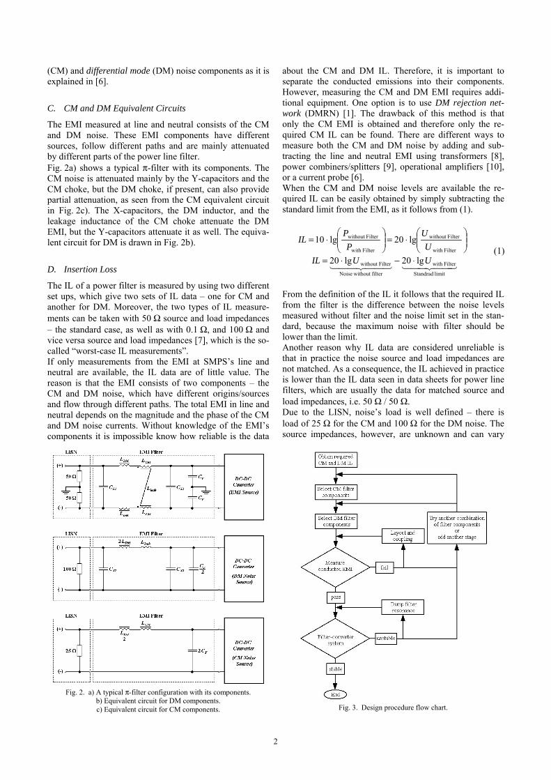
The EMI measured at line and neutral consists of the CM and DM noise. These EMI components have different sources, follow different paths and are mainly attenuated by different parts of the power line filter. Fig. 2a) shows a typical π-filter with its components. The CM noise is attenuated mainly by the Y-capacitors and the CM choke, but the DM choke, if present, can also provide partial attenuation, as seen from the CM equivalent circuit in Fig. 2c). The X-capacitors, the DM inductor, and the leakage inductance of the CM choke attenuate the DM EMI, but the Y-capacitors attenuate it as well. The equiva-lent circuit for DM is drawn in Fig. 2b).
D. Insertion Loss
The IL of a power filter is measured by using two different set ups, which give two sets of IL data – one for CM and another for DM. Moreover, the two types of IL measure-ments can be taken with 50 Ω source and load impedances – the standard case, as well as with 0.1 Ω, and 100 Ω and vice versa source and load impedances [7], which is the so-called “worst-case IL measurements”. If only measurements from the EMI at SMPS’s line and neutral are available, the IL data are of little value. The reason is that the EMI consists of two components – the CM and DM noise, which have different origins/sources and flow through different paths. The total EMI in line and neutral depends on the magnitude and the phase of the CM and DM noise currents. Without knowledge of the EMI’s components it is impossible know how reliable is the data
about the CM and DM IL. Therefore, it is important to separate the conducted emissions into their components. However, measuring the CM and DM EMI requires addi-tional equipment. One option is to use DM rejection net-work (DMRN) [1]. The drawback of this method is that only the CM EMI is obtained and therefore only the re-quired CM IL can be found. There are different ways to measure both the CM and DM noise by adding and sub-tracting the line and neutral EMI using transformers [8], power combiners/splitters [9], operational amplifiers [10], or a current probe [6]. When the CM and DM noise levels are available the re-quired IL can be easily obtained by simply subtracting the standard limit from the EMI, as it follows from (1).
44 344 2144 344 21
limit Standrad
Filterwith
filter without Noise
Filterwithout
Filterwith
Filterwithout
Filterwith
Filterwithout
lg20lg20
lg20lg10
UUILU
UP
PIL
⋅−⋅=
⎟⎟⎠
⎞⎜⎜⎝
⎛⋅=⎟⎟
⎠
⎞⎜⎜⎝
⎛⋅=
(1)
From the definition of the IL it follows that the required IL from the filter is the difference between the noise levels measured without filter and the noise limit set in the stan-dard, because the maximum noise with filter should be lower than the limit. Another reason why IL data are considered unreliable is that in practice the noise source and load impedances are not matched. As a consequence, the IL achieved in practice is lower than the IL data seen in data sheets for power line filters, which are usually the data for matched source and load impedances, i.e. 50 Ω / 50 Ω. Due to the LISN, noise’s load is well defined – there is load of 25 Ω for the CM and 100 Ω for the DM noise. The source impedances, however, are unknown and can vary
Fig. 2. a) A typical π-filter configuration with its components. b) Equivalent circuit for DM components. c) Equivalent circuit for CM components.
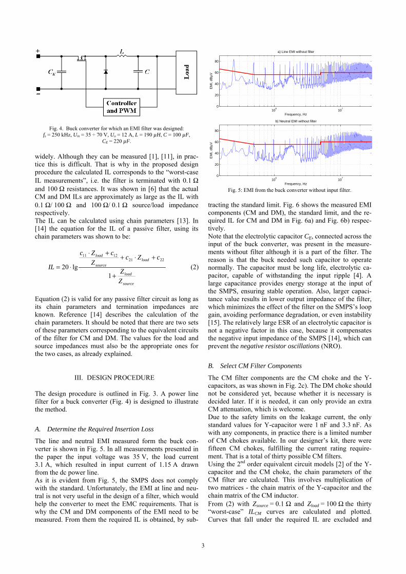
Fig. 3. Design procedure flow chart.
2
widely. Although they can be measured [1], [11], in prac-tice this is difficult. That is why in the proposed design procedure the calculated IL corresponds to the “worst-case IL measurements”, i.e. the filter is terminated with 0.1 Ω and 100 Ω resistances. It was shown in [6] that the actual CM and DM ILs are approximately as large as the IL with 0.1 Ω/ 100 Ω and 100 Ω/ 0.1 Ω source/load impedance respectively.
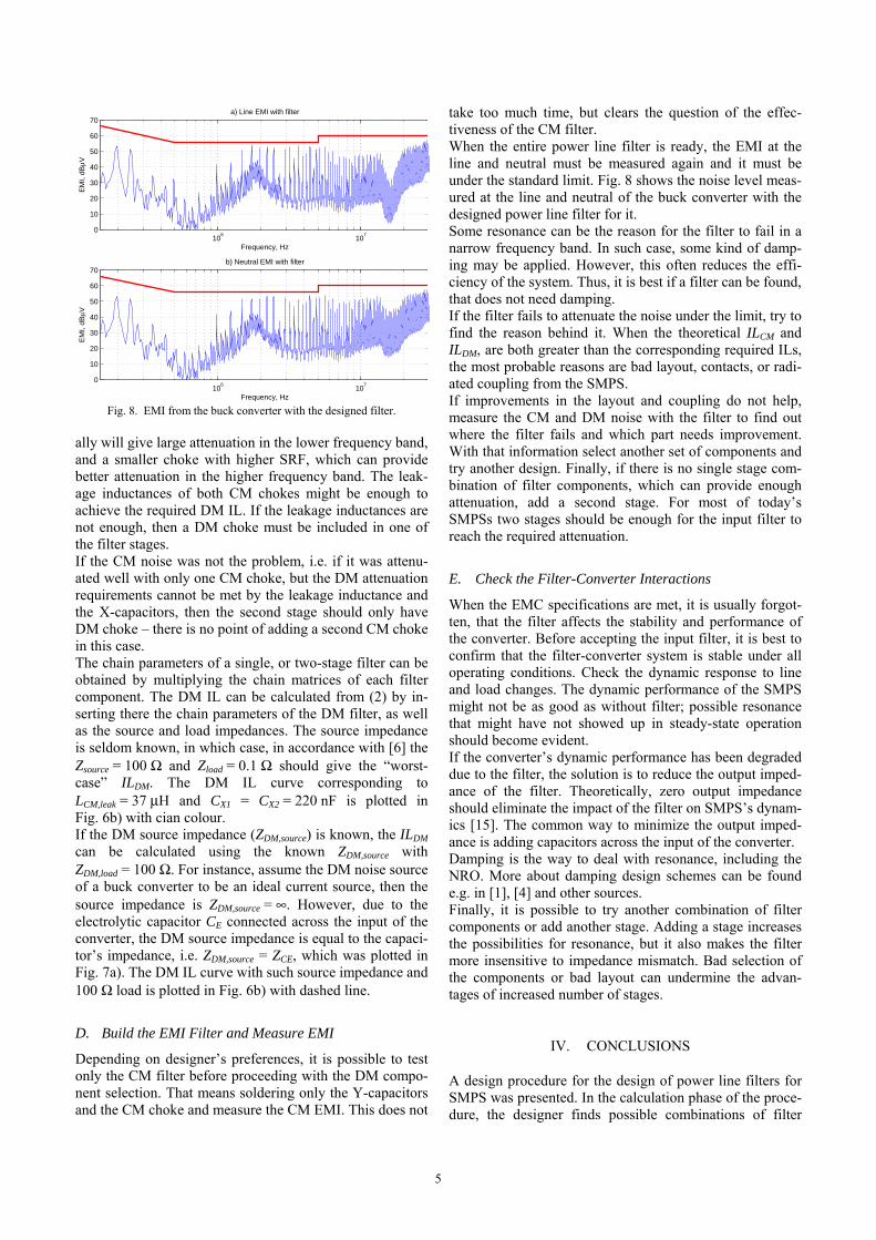
Fig. 4. Buck converter for which an EMI filter was designed:
fs = 250 kHz, Uin = 35 ÷ 70 V, Uo = 12 A, L = 190 µH, C = 100 µF, CE = 220 µF.
The IL can be calculated using chain parameters [13]. In [14] the equation for the IL of a passive filter, using its chain parameters was shown to be:
source
load
loadsource
load
ZZ
cZcZ
cZc
IL+
+⋅++⋅
⋅=1
lg202221
1211
(2)
Equation (2) is valid for any passive filter circuit as long as its chain parameters and termination impedances are known. Reference [14] describes the calculation of the chain parameters. It should be noted that there are two sets of these parameters corresponding to the equivalent circuits of the filter for CM and DM. The values for the load and source impedances must also be the appropriate ones for the two cases, as already explained.
III. DESIGN PROCEDURE
The design procedure is outlined in Fig. 3. A power line filter for a buck converter (Fig. 4) is designed to illustrate the method.
A. Determine the Required Insertion Loss
The line and neutral EMI measured form the buck con-verter is shown in Fig. 5. In all measurements presented in the paper the input voltage was 35 V, the load current 3.1 A, which resulted in input current of 1.15 A drawn from the dc power line. As it is evident from Fig. 5, the SMPS does not comply with the standard. Unfortunately, the EMI at line and neu-tral is not very useful in the design of a filter, which would help the converter to meet the EMC requirements. That is why the CM and DM components of the EMI need to be measured. From them the required IL is obtained, by sub-
tracting the standard limit. Fig. 6 shows the measured EMI components (CM and DM), the standard limit, and the re-quired IL for CM and DM in Fig. 6a) and Fig. 6b) respec-tively.
106
107
0
20
40
60
80
a) Line EMI without filter
Frequency, Hz
EM
I, dB
µV
106
107
0
20
40
60
80
b) Neutral EMI without filter
Frequency, Hz
EM
I, dB
µV
Fig. 5: EMI from the buck converter without input filter.
Note that the electrolytic capacitor CE, connected across the input of the buck converter, was present in the measure-ments without filter although it is a part of the filter. The reason is that the buck needed such capacitor to operate normally. The capacitor must be long life, electrolytic ca-pacitor, capable of withstanding the input ripple [4]. A large capacitance provides energy storage at the input of the SMPS, ensuring stable operation. Also, larger capaci-tance value results in lower output impedance of the filter, which minimizes the effect of the filter on the SMPS’s loop gain, avoiding performance degradation, or even instability [15]. The relatively large ESR of an electrolytic capacitor is not a negative factor in this case, because it compensates the negative input impedance of the SMPS [14], which can prevent the negative resistor oscillations (NRO).
B. Select CM Filter Components
The CM filter components are the CM choke and the Y-capacitors, as was shown in Fig. 2c). The DM choke should not be considered yet, because whether it is necessary is decided later. If it is needed, it can only provide an extra CM attenuation, which is welcome. Due to the safety limits on the leakage current, the only standard values for Y-capacitor were 1 nF and 3.3 nF. As with any components, in practice there is a limited number of CM chokes available. In our designer’s kit, there were fifteen CM chokes, fulfilling the current rating require-ment. That is a total of thirty possible CM filters. Using the 2nd order equivalent circuit models [2] of the Y-capacitor and the CM choke, the chain parameters of the CM filter are calculated. This involves multiplication of two matrices - the chain matrix of the Y-capacitor and the chain matrix of the CM inductor. From (2) with Zsource = 0.1 Ω and Zload = 100 Ω the thirty “worst-case” ILCM curves are calculated and plotted. Curves that fall under the required IL are excluded and
3

what is left is a set of theoretically “good CM filters”, from which the designer should select one to start with. The first choice does not have to be the CM filter with highest IL, but one that best satisfies designer’s objectives. For exam-ple, among the combinations providing good ILCM, i.e. which are well above the required one, the designer might chose one with minimum size, or one which would be the cheapest. In case of a failure with the first filter, the designer can eventually try another combination from the set of “good CM filters”. The formation of this set limits the trial-and-error possibilities. In addition, the set of IL curves gives some hints of the weaker and stronger sides of each combi-nation of filter components. Plotting the CM IL curves does not take much time. With ready software code and filter components data entered in the computer, the process can take a few minutes – just selecting the Y-capacitors and CM chokes, fulfilling the safety and rating requirements and the software plots the corresponding curves. In our example, none of the calculated ILCM curves is above the required CM IL in the entire frequency range, but nev-ertheless some good CM filter combinations can be se-lected. The calculated ILCM curves show that the filters with CY = 3.3 nF perform poorly in the higher frequency range due to capacitor’s low self-resonant frequency (SRF), which is about 20 MHz [16]. In contrast, the 1 nF Y-capacitor has SRF about 42 MHz, which results in better performance at higher frequencies. In general, the CM chokes used in this work [17], have higher SRF, between 800 kHz and 2 MHz, when the cur-rent ratings are higher and inductance values are lower. Consequently, filters with low LCM, and higher rating at-tenuate better at higher frequencies, but that is at the ex-pense of the lower frequencies, where they perform poorly. At this phase, however, preference should be given to the lower frequency band. The reason is that the performance of the filter at higher frequencies depends mostly upon the layout and parasitic coupling – issues that are better dealt with at the practical stage of the design. With these consid-
erations in mind a good compromise was a CM filter con-sisting of 4.2 mH / 1 nF. This combination provides the required CM IL with enough margin at lower frequency band. Chokes with larger inductance have even larger IL, but are even worse in the higher frequency band.
106
107
0
20
40
60
80
100
Frequency, Hz
EM
I, dB
µV
a) CM EMI without filter
Measured CM EMIRequired CM ILCalculated CM IL for 0.1Ω/ 100Ω
106
107
0
20
40
60
80
100
Frequency, Hz
EM
I, dB
µV
b) DM EMI without filter
Measured DM EMIRequired DM ILCalculated DM IL for 100Ω/ 0.1ΩCalculated DM IL for Z
e/ 100Ω
Fig. 6. Measured CM and DM EMI, required CM and DM IL, and se-lected theoretical CM and DM IL curve.
104
105
106
107
108
10−2
100
102
104
106
Frequency, Hz
Impe
danc
e, Ω
a) Capacitors′ Impedance
X−CapacitorsY−CapacitorsElectr. Cap.
104
105
106
107
108
100
102
104
106
108
Frequency, Hz
Impe
danc
e, Ω
b) Inductors′ Impedance
CM InductorCM Leak Ind
Fig. 7. Theoretical impedances of the components used in the filter.
Fig. 6a) shows the measured CM EMI (blue), the required CM IL (green), and the calculated “worst-case” CM IL curve (cyan), corresponding to the selected CM filter. The theoretical impedances of the CM components are plotted in Fig. 7 along with the impedance of the electrolytic ca-pacitor CE and the DM components, which are discussed later.
C. Select DM Filter Components
It was mentioned that the CM choke’s leakage inductance plays role in the DM noise attenuation. A lot of space could be saved, if DM choke could be avoided. This explains why the leakage inductance of the CM choke is sometimes intentionally increased [3]. An effort to try to achieve the DM attenuation without using DM choke is justified. Therefore, at first the DM IL is calculated taking only the leakage inductance of the CM choke into account. The leakage inductance of the CM choke selected in our example was measured to be 37 µH. Keeping the parasitic capacitance same as it is for the CM choke and resistance twice the path resistance, results in the impedance shown in Fig. 7b) with a green line. For the π-filter in Fig. 2b), with CX1 = CX2, there are seven ILDM curves, each corresponding to one of the seven X-capacitors available in the designer’s kit used in this work. Similarly to the CM case, the IL curves above the required DM IL, if any, form the set of “good DM filters”. If there are no such, a DM choke will most probably be needed. In such case, it is best considering a two-stage filter topology. If the required CM IL was not achieved with the single stage topology, it might be that two CM chokes – one in each stage will provide the necessary attenuation. In two stage topologies with two CM chokes, it is best to combine them in such a way that they complement each other. For example, one of the chokes can be of large LCM, which usu-
4
ally will give large attenuation in the lower frequency band, and a smaller choke with higher SRF, which can provide better attenuation in the higher frequency band. The leak-age inductances of both CM chokes might be enough to achieve the required DM IL. If the leakage inductances are not enough, then a DM choke must be included in one of the filter stages. If the CM noise was not the problem, i.e. if it was attenu-ated well with only one CM choke, but the DM attenuation requirements cannot be met by the leakage inductance and the X-capacitors, then the second stage should only have DM choke – there is no point of adding a second CM choke in this case. The chain parameters of a single, or two-stage filter can be obtained by multiplying the chain matrices of each filter component. The DM IL can be calculated from (2) by in-serting there the chain parameters of the DM filter, as well as the source and load impedances. The source impedance is seldom known, in which case, in accordance with [6] the Zsource = 100 Ω and Zload = 0.1 Ω should give the “worst-case” ILDM. The DM IL curve corresponding to LCM,leak = 37 µH and CX1 = CX2 = 220 nF is plotted in Fig. 6b) with cian colour. If the DM source impedance (ZDM,source) is known, the ILDM can be calculated using the known ZDM,source with ZDM,load = 100 Ω. For instance, assume the DM noise source of a buck converter to be an ideal current source, then the source impedance is ZDM,source = ∞. However, due to the electrolytic capacitor CE connected across the input of the converter, the DM source impedance is equal to the capaci-tor’s impedance, i.e. ZDM,source = ZCE, which was plotted in Fig. 7a). The DM IL curve with such source impedance and 100 Ω load is plotted in Fig. 6b) with dashed line.
D. Build the EMI Filter and Measure EMI
Depending on designer’s preferences, it is possible to test only the CM filter before proceeding with the DM compo-nent selection. That means soldering only the Y-capacitors and the CM choke and measure the CM EMI. This does not
take too much time, but clears the question of the effec-tiveness of the CM filter. When the entire power line filter is ready, the EMI at the line and neutral must be measured again and it must be under the standard limit. Fig. 8 shows the noise level meas-ured at the line and neutral of the buck converter with the designed power line filter for it. Some resonance can be the reason for the filter to fail in a narrow frequency band. In such case, some kind of damp-ing may be applied. However, this often reduces the effi-ciency of the system. Thus, it is best if a filter can be found, that does not need damping. If the filter fails to attenuate the noise under the limit, try to find the reason behind it. When the theoretical ILCM and ILDM, are both greater than the corresponding required ILs, the most probable reasons are bad layout, contacts, or radi-ated coupling from the SMPS. If improvements in the layout and coupling do not help, measure the CM and DM noise with the filter to find out where the filter fails and which part needs improvement. With that information select another set of components and try another design. Finally, if there is no single stage com-bination of filter components, which can provide enough attenuation, add a second stage. For most of today’s SMPSs two stages should be enough for the input filter to reach the required attenuation.
106
107
0
10
20
30
40
50
60
70a) Line EMI with filter
Frequency, Hz
EM
I, dB
µV
106
107
0
10
20
30
40
50
60
70b) Neutral EMI with filter
Frequency, Hz
EM
I, dB
µV
Fig. 8. EMI from the buck converter with the designed filter.
E. Check the Filter-Converter Interactions
When the EMC specifications are met, it is usually forgot-ten, that the filter affects the stability and performance of the converter. Before accepting the input filter, it is best to confirm that the filter-converter system is stable under all operating conditions. Check the dynamic response to line and load changes. The dynamic performance of the SMPS might not be as good as without filter; possible resonance that might have not showed up in steady-state operation should become evident. If the converter’s dynamic performance has been degraded due to the filter, the solution is to reduce the output imped-ance of the filter. Theoretically, zero output impedance should eliminate the impact of the filter on SMPS’s dynam-ics [15]. The common way to minimize the output imped-ance is adding capacitors across the input of the converter. Damping is the way to deal with resonance, including the NRO. More about damping design schemes can be found e.g. in [1], [4] and other sources. Finally, it is possible to try another combination of filter components or add another stage. Adding a stage increases the possibilities for resonance, but it also makes the filter more insensitive to impedance mismatch. Bad selection of the components or bad layout can undermine the advan-tages of increased number of stages.
IV. CONCLUSIONS
A design procedure for the design of power line filters for SMPS was presented. In the calculation phase of the proce-dure, the designer finds possible combinations of filter
5
components, which can be compared to provide a good starting point for the practical design. The theoretical at-tenuation curves provide some guidelines for eventual changes or adjustments in the selection of filter compo-nents, which minimizes the number of practical designs to find the desired one. An example of an EMI filter for a buck converter was de-signed to illustrate the proposed method. As expected, the buck converter with the designed filter meets the require-ments set in the standard.
REFERENCES
[1] M. L. Nave, Power Line Filter Design for Switch-Mode Power Sup-plies, Van Nostrand Reinold, 1991, pp. 210.
[2] L. Tihanyi, Electromagnetic Compatibility in Power Electronics, IEEE Press, Inc., 1995, pp. 403
[3] R. L. Ozenbaugh, EMI Filter Design, Marcel Dekker, Inc., 1996, pp. 252.
[4] D. M. Mitchell, “Power line filter design considerations for dc-dc converters,” IEEE Industry Application Magazine, vol. 5, issue 6, 1999, pp. 16-26.
[5] F.-Y. Shin, D. Y. Chen, Y.-P. Wu, and Y.-T. Chen, “A Procedure for Designing EMI Filters for AC Line Applications”, IEEE Transac-tions on Power Electronics, vol. 11 , January 1996, pp. 170-181.
[6] K. Kostov, J.-P. Sjöroos, J. Kyyrä, and T. Suntio, ”Selection of Power Filters for Switched Mode Power Supplies,” 4th Nordic Workshop on Power and Industrial Electronics, Trondheim, June, 2004.
[7] CISPR 17 Measurements, Application Note 690-264A, Schaffner,
1996. [8] C. R. Paul and K. B. Hardin, “Diagnosis and Reduction of Con-
ducted Noise Emissions”, IEEE Transactions on Electromagnetic Compatibility, vol. 30, November 1988, pp. 553-560.
[9] T. Guo, D. Y. Chen, and F. C. Lee, “Separation of the Common-Mode and Differential Mode Conducted EMI Noise”, IEEE Trans-actions on Power Electronics, vol. 11, May 1996, pp. 480-488.
[10] T. V. Rauner, “A Measurement System for Evaluation of the Cou-pling Modes and Mechanisms of Conductive Noise”, Master’s The-sis, Helsinki University of Technology, 1997, pp. 64.
[11] L. M. Schneider, “Noise Source Equivalent Circuit Model for Off-Line Converters and its Use in Input Filter Design”, Proceedings of Powercon, 1983, pp. 167-175.
[12] M. C. Caponet, F. Profumo, L. Ferraris, A. Bertoz, and D. Marzella, ”Common and Differential Mode Noise Separation: Comparison of two Different Approaches”, IEEE 32nd Annual Power Electronics Specialists Conference, vol. 3, June, 2001, pp. 1383–1388.
[13] W.-K. Chen, et al., The Circuits and Filters Handbook, IEEE Press, Inc., 1995, pp. 2861.
[14] K. S. Kostov, J. Kyyrä, and T. Suntio, “Analysis and Design of EMI Filters for DC-DC Converters Using Chain Parameters”, European Power Electronics Conference, Toulouse, September 2003.
[15] T. Suntio, T. Tepsa, K. Kostov, and J. Kyyrä, “EMI Filter Design Issues in Switched-Mode Converter Applications”, Proceedings of PCIM, vol. 2, Nürnberg, Germany, May, 2004, pp. 830-835.
[16] MKP 336 6 Y2, Interference Suppression Film Capacitors, Vishay BCcomponents, August 2003.
[17] EMC Components, Publication 690-626B, Schaffner, 2001.
6