The Ripple Effect: Biofuels, Food Security, and the Environment
DC-link Voltage Ripple Compensation forMultilevel Active-Neutral-Point-Clamped Converters
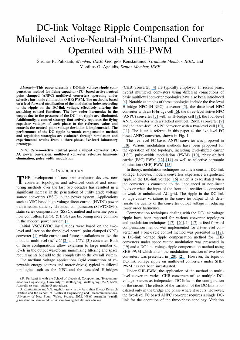
© 2012 IEEE IEEE Transactions on Power Delivery, Vol. 27. No. 4, pp. 2176-2484, 2012 DC-link Voltage Ripple Compensation for Multilevel Active-Neutral-Point-Clamped Converters Operated with SHE-PWM Sridhar R. Pulikanti Georgios Konstantinou Vassilios G. Agelidis This material is posted here with permission of the IEEE. Such permission of the IEEE does not in any way imply IEEE endorsement of any of UNSW’s products or services. Internal or personal use of this material is permitted. However, permission to reprint/republish this material for advertising or promotional purposes or for creating new collective works for resale or redistribution must be obtained from the IEEE by writing to: [email protected] By choosing to view this document, you agree to all provisions of the copyright laws protecting it.
1
DC-link Voltage Ripple Compensation forMultilevel Active-Neutral-Point-Clamped Converters
Operated with SHE-PWMSridhar R. Pulikanti, Member, IEEE, Georgios Konstantinou, Graduate Member, IEEE, and
Vassilios G. Agelidis, Senior Member, IEEE
Abstract—This paper presents a DC-link voltage ripple com-pensation method for flying capacitor (FC) based active neutralpoint clamped (ANPC) multilevel converters operating underselective harmonic elimination (SHE) PWM. The method is basedon a feed-forward modification of the modulation index accordingto the ripple on the DC-link voltage, effectively altering theswitching control functions. The low order harmonics in theoutput due to the presence of the DC-link ripple are eliminated.Additionally, a control strategy that actively regulates the flyingcapacitor voltages of each phase to the reference value andcontrols the neutral point voltage deviation is implemented. Theperformance of the DC ripple harmonic compensation methodand regulation strategies are evaluated through simulation andexperimental results from a three-phase, five-level laboratoryprototype.
Index Terms—Active neutral point clamped converter, DC-AC power conversion, multilevel converter, selective harmonicelimination, pulse width modulation
I. INTRODUCTION
THE development of new semiconductor devices, newconverter topologies and advanced control and moni-
toring methods over the last two decades has resulted in asignificant increase in the penetration of utility grade voltagesource converters (VSC) in the power system. Applicationssuch as VSC-based high-voltage direct-current (HVDC) powertransmission, static synchronous compensators (STATCOMs),static series compensators (SSSC), unified and interline powerflow controllers (UPFC & IPFC) are becoming more commonin the modern power system [1].
Initial VSC-HVDC installations were based on the two-level and later on the three-level neutral point clamped (NPC)converter [1] while current and future installations utilize themodular multilevel (M2LC [2] and CTL [3]) converter. Bothof these configurations allow extension to large number oflevels in the output waveforms minimizing filtering and spacerequirements but add to the complexity to the overall system.
For medium voltage applications (grid connection of re-newable energy sources and motor drives) typical multileveltopologies such as the NPC and the cascaded H-bridges
S.R. Pulikanti is with the School of Electrical, Computer and Telecommu-nications Engineering, University of Wollongong, Wollongong, 2522, NSW,Australia (e-mail: [email protected])
G. Konstantinou and V.G. Agelidis are with the Australian Energy ResearchInstitute and the School of Electrical Engineering and Telecommunications,University of New South Wales, Sydney, 2052, NSW, Australia (e-mail:[email protected] & [email protected])
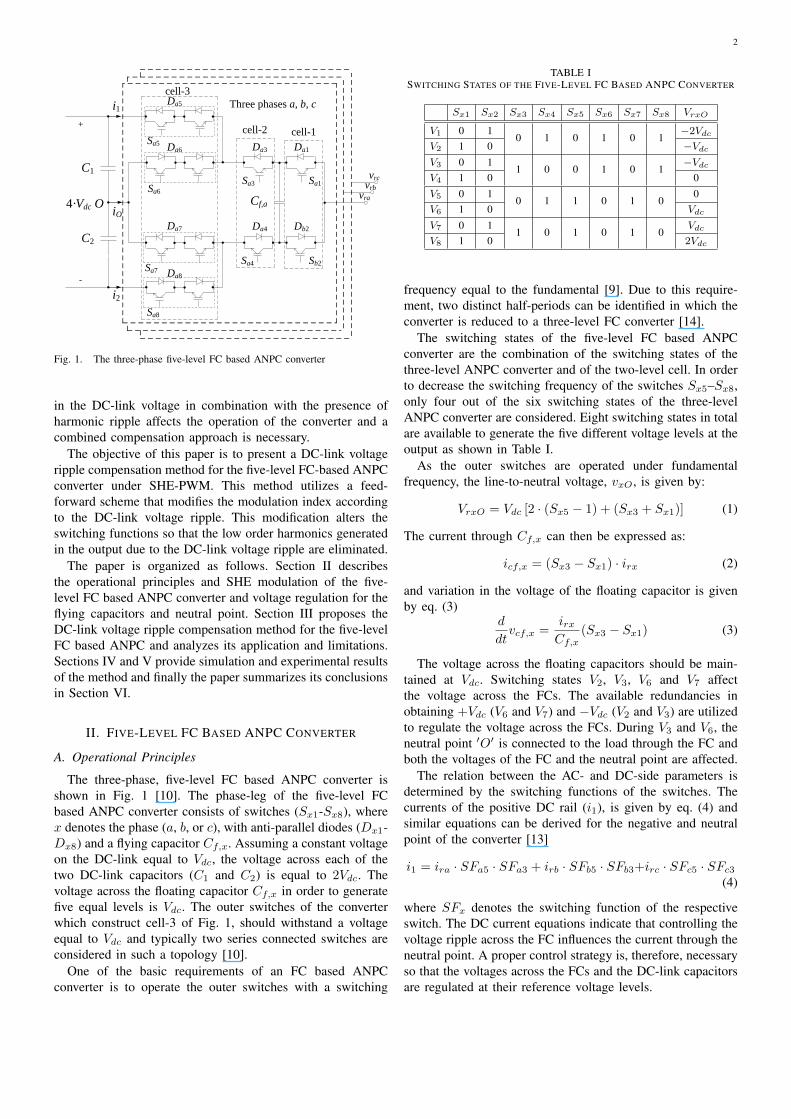
(CHB) converter [4] are typically employed. In recent years,hybrid multilevel converters using different connections ofbasic multilevel converter topologies have also been introduced[4]. Notable examples of these topologies include the five-levelH-bridge NPC (H-NPC) converter [5], the three-level NPCconverter with an H-bridge cell [6], the three-level active NPC(ANPC) converter [7] with an H-bridge cell [8], the four-levelANPC converter with a stacked multicell (SMC) converter [9]and the three-level ANPC converter with a two-level cell [10],[11]. The latter is referred in this paper as the five-level FCbased ANPC converter, shown in Fig. 1.
The five-level FC based ANPC converter was proposed in[10]. Various modulation methods have been proposed forthe operation of the topology, including level-shifted carrier(LSC) pulse-width modulation (PWM) [10], phase-shiftedcarrier (PSC) PWM [12]–[14] as well as selective harmonicelimination (SHE) PWM [15].
In theory, modulation techniques assume a constant DC-linkvoltage. However, modern converters experience a significantripple in the DC-link voltage [16] which is exacerbated whenthe converter is connected to the unbalanced or non-linearloads or when the input of the front-end rectifier is connectedto weak or unbalanced AC grid. The ripple in the DC-linkvoltage causes variations in the converter output which dete-riorate the quality of the converter output voltage introducinglower order harmonics.
Compensation techniques dealing with the DC-link voltageripple have been reported for various converter topologiesand modulation techniques [17]- [20]. In [17], a feed-forwardcompensation method was implemented for a two-level con-verter and a one-cycle control method was presented in [18].A DC-link voltage ripple compensation method for CHBconverters under space vector modulation was presented in[19] and a DC-link voltage ripple compensation method usingSHE-PWM which alters the modulation function of two-levelconverters was presented in [20], [21]. However, the topic ofDC-link voltage ripple on multilevel converters under SHE-PWM has not been investigated.
Under SHE-PWM, the application of the method to multi-level converters varies. CHB converters utilize multiple DC-voltage sources as independent DC-links in the configurationof the circuit. The effects of the variation of the DC-link is lo-calized only in the bridge and phase where it occurs. However,the five-level FC based ANPC converter requires a single DC-link for the operation of the three-phase topology. Variation
2
C1
C2
O
+
-
4·Vdc Cf,a
Sa3
Sa4
Sa1
Sb2
vrc
Da3 Da1
Da4 Db2
Da5
Sa6
Da6
Sa7
Da7
Sa8
Da8
Sa5
iO
i1
i2
vravrb
cell-1cell-2
cell-3Three phases a, b, c
Fig. 1. The three-phase five-level FC based ANPC converter
in the DC-link voltage in combination with the presence ofharmonic ripple affects the operation of the converter and acombined compensation approach is necessary.
The objective of this paper is to present a DC-link voltageripple compensation method for the five-level FC-based ANPCconverter under SHE-PWM. This method utilizes a feed-forward scheme that modifies the modulation index accordingto the DC-link voltage ripple. This modification alters theswitching functions so that the low order harmonics generatedin the output due to the DC-link voltage ripple are eliminated.
The paper is organized as follows. Section II describesthe operational principles and SHE modulation of the five-level FC based ANPC converter and voltage regulation for theflying capacitors and neutral point. Section III proposes theDC-link voltage ripple compensation method for the five-levelFC based ANPC and analyzes its application and limitations.Sections IV and V provide simulation and experimental resultsof the method and finally the paper summarizes its conclusionsin Section VI.
II. FIVE-LEVEL FC BASED ANPC CONVERTER
A. Operational Principles
The three-phase, five-level FC based ANPC converter isshown in Fig. 1 [10]. The phase-leg of the five-level FCbased ANPC converter consists of switches (Sx1-Sx8), wherex denotes the phase (a, b, or c), with anti-parallel diodes (Dx1-Dx8) and a flying capacitor Cf,x. Assuming a constant voltageon the DC-link equal to Vdc, the voltage across each of thetwo DC-link capacitors (C1 and C2) is equal to 2Vdc. Thevoltage across the floating capacitor Cf,x in order to generatefive equal levels is Vdc. The outer switches of the converterwhich construct cell-3 of Fig. 1, should withstand a voltageequal to Vdc and typically two series connected switches areconsidered in such a topology [10].
One of the basic requirements of an FC based ANPCconverter is to operate the outer switches with a switching
TABLE ISWITCHING STATES OF THE FIVE-LEVEL FC BASED ANPC CONVERTER
Sx1 Sx2 Sx3 Sx4 Sx5 Sx6 Sx7 Sx8 VrxO
V1 0 10 1 0 1 0 1
−2Vdc
V2 1 0 −VdcV3 0 1
1 0 0 1 0 1−Vdc
V4 1 0 0
V5 0 10 1 1 0 1 0
0V6 1 0 Vdc
V7 0 11 0 1 0 1 0
Vdc
V8 1 0 2Vdc
frequency equal to the fundamental [9]. Due to this require-ment, two distinct half-periods can be identified in which theconverter is reduced to a three-level FC converter [14].
The switching states of the five-level FC based ANPCconverter are the combination of the switching states of thethree-level ANPC converter and of the two-level cell. In orderto decrease the switching frequency of the switches Sx5–Sx8,only four out of the six switching states of the three-levelANPC converter are considered. Eight switching states in totalare available to generate the five different voltage levels at theoutput as shown in Table I.
As the outer switches are operated under fundamentalfrequency, the line-to-neutral voltage, vxO, is given by:
VrxO = Vdc [2 · (Sx5 − 1) + (Sx3 + Sx1)] (1)
The current through Cf,x can then be expressed as:
icf,x = (Sx3 − Sx1) · irx (2)
and variation in the voltage of the floating capacitor is givenby eq. (3)
d
dtvcf,x =
irxCf,x
(Sx3 − Sx1) (3)
The voltage across the floating capacitors should be main-tained at Vdc. Switching states V2, V3, V6 and V7 affectthe voltage across the FCs. The available redundancies inobtaining +Vdc (V6 and V7) and −Vdc (V2 and V3) are utilizedto regulate the voltage across the FCs. During V3 and V6, theneutral point ′O′ is connected to the load through the FC andboth the voltages of the FC and the neutral point are affected.
The relation between the AC- and DC-side parameters isdetermined by the switching functions of the switches. Thecurrents of the positive DC rail (i1), is given by eq. (4) andsimilar equations can be derived for the negative and neutralpoint of the converter [13]
i1 = ira · SFa5 · SFa3 + irb · SFb5 · SFb3+irc · SFc5 · SFc3
(4)
where SFx denotes the switching function of the respectiveswitch. The DC current equations indicate that controlling thevoltage ripple across the FC influences the current through theneutral point. A proper control strategy is, therefore, necessaryso that the voltages across the FCs and the DC-link capacitorsare regulated at their reference voltage levels.

3
B. SHE-PWM for five-level converters
SHE methods for multilevel PWM waveforms have beenreported in [22]– [24]. The five-level waveform with Ntransitions per quarter-period is pre-calculated in such a waythat a number of (N -1) low-order harmonics are eliminatedfrom the output spectrum while the fundamental frequencycomponent is controlled to the required level.
A set of equations are solved to obtain solutions for theswitching transitions [23]. In a generalized form, the systemof equations is as follows:
N1∑i=1
(−1)i−1 cos(ai) +
N∑i=N1+1
(−1)i−(1+N1) cos(ai) = M
(5)N1∑i=1
(−1)i−1 cos(nai) +
N∑i=N1+1
(−1)i−(1+N1) cos(nai) = 0
(6)where n = 5, 7, . . . , 3N − 2 and N is odd
0 ≤M ≤ 2 (7)
If A1 is the amplitude of the fundamental component to begenerated, then
A1 =4Vdcπ
·M (8)
0 < α1 < α2 < . . . < αk+m <π
2(9)
where M is the modulation index and N1 + N2 = N ,N1 is the number of switchings, or angles placed between0p.u. and 1p.u. levels and N2 is the number of waveformtransitions placed between 1p.u and 2p.u. levels and αi it thei-th switching angle in the quarter-period of the waveform. Bysolving system of eqns. (5)–(6) with the constraint of eqn. (9),the required solutions can be obtained.
For different distribution ratios N1/N2, a different set ofequations describing new waveforms are solved [23], [24]providing multiple solutions. The multiple sets obtained, over-lap for different N1/N2 ratios over the range of modulationindices. The multiple solutions available for the five-level caseare presented in [23].
C. Flying Capacitor Voltage Regulation
The charging and discharging of the FC takes place at themiddle voltage levels ±1p.u. when the load current flowsthrough the FC and depends upon its direction. The voltageacross the FC, which should be maintained at ±1p.u., isaffected by switching states V2, V3, V6, and V7 and canbe regulated using the switching states that result in timeintervals of charging and discharging being equal over afundamental period. Due to symmetrical pulse patterns overthe quarter of the period, equal time intervals of charging anddischarging over a fundamental period can be achieved. Amore detailed explanation of the control strategy, the SHE-PWM implementation and gating signal generation is givenin [15].
III. VOLTAGE RIPPLE COMPENSATION
A. Effect of DC-link harmonic ripple
The Fourier analysis of the converter phase voltages undera constant DC-link voltage is
¯SW =
∞∑m=1
An sin(nω1t)
∞∑m=1
An sin(nω1t−2π
3)
∞∑m=1
An sin(nω1t−4π
3)
(10)
where the coefficients of the n-th harmonic are calculatedthrough eqs. (5)–(6). Assuming a ripple harmonic frequencyfr = 2πrω1 and the magnitude of 4R · Vdc in the DC-linkvoltage, given by eq. (11), low order harmonics are generatedin the output AC voltage due to the interaction of the spectralcomponents of the output voltage (eq. (10)) and the DC-linkharmonics.
V ′dc = 4 · Vdc (1 +R sin(rωt)) (11)
The harmonics due to the DC-link ripple are located atfrequencies (n−r)ω1 and (n+r)ω1 as sidebands to the spectralcomponents of the output voltage of eq. (10). The amplitudeof the harmonics generated at n + r and n − r are in directcorrelation to the amplitude of the n-th harmonic (An) andtheir normalized amplitude given by (2R)·An
2 .The amplitudes An of the harmonics are well-defined
through the SHE-PWM formulation of eqs (5) and (6) and thesolutions used in each application. These additional harmonicsalso vary in terms of their sequence. The sequence of thespectral components due to the (n + r) terms in the output,and since the DC-link voltage is common for all three-phases,remain the same as in the n-th harmonic. However, thesequence of the spectral components due to the (n− r) termsdepend on the values of n and r. If n > r then the sequenceof the components remains the same with that of the n-thharmonic but if n < r the harmonics generated have invertedsequences and a positive sequence n-th harmonic generatesnegative sequence (n−r)–th harmonic, a negative sequence n-th harmonic (if present) generates a positive sequence (n−r)thharmonic while zero sequence harmonics are not affected.
This can be a major issue as the interaction of low orderharmonics with the fundamental frequency component (inwhich case n = 1 and r > 1) generates quite significant nega-tive sequence components in the output voltage. Additionally,when n − r = ±1, spectral components in the fundamentalfrequency are generated affecting the balancing of the phasevoltages in the output of the converter. These harmonics canbe of positive, negative or zero sequence depending on thecombination of n and r.
B. ANPC Voltage Ripple Compensation
The main difference in the application of ripple com-pensation methods in the ANPC converter when comparedto other multilevel topologies is the common DC-link for
4
all three phases of the converter and the redundancies inacquiring intermediate levels of the waveform. Both of thesedifferences need to be considered for the DC-link voltageripple compensation method.
When the converter generates either the top or the bottomlevel in the waveform V1 and V8, the DC-link appears directlyin the output of the phase and the waveform follows thewaveform of eq. (11). However, when the levels ±Vdc appearin the output and the DC-link is connected to the output (V2and V7), the actual level of the waveform is
V±Vdc= 2 · Vdc [1 +R · sin(rωt)] − VCfc
(12)
Considering that the voltage of the flying capacitor is regulatedto the reference voltage of Vdc, the DC-link ripple appears inthe output as double the amplitude of the level of the converter
V±Vdc= Vdc [1 + 2 ·R · sin(rωt)] (13)
The remaining states (V3 and V6) for this level do not requirethe DC-link voltage but are generated through the neutralpoint of the converter and the flying capacitor. The ripple ofthe DC-link does not affect this voltage level and hence nocompensation is required for these states.
The compensation method is based on a feed-forward mod-ification of the switching function of the converter based onthe average and instantaneous values of the DC-link voltage[20]. The modulating function of the converter M is modifiedso that the ripple in the DC-link does not generate low orderharmonics as
M ′ =M(t)VdcVlevel
(14)
In the five-level FC based ANPC converter, this is separatedin three distinct occasions. When the output of the converteris ±2Vdc, then the modulation index is modified based oneq. (12) and the modulating waveform is
M ′±2Vdc(t) =
M(t)
1 +R · sin(rωt)(15)
When the output of the converter is equal to ±Vdc, then whenthe converter switching state connects the output to the neutralpoint and the FC then the converter switching function is notmodified (V3 and V6) and
M ′±VdcA(t) = M(t) (16)
whereas when the states that connect the DC-link to the outputare used (V2 and V7), the modified modulation function isgiven by
M ′±VdcB(t) =
M(t)
1 + 2R · sin(rωt)(17)
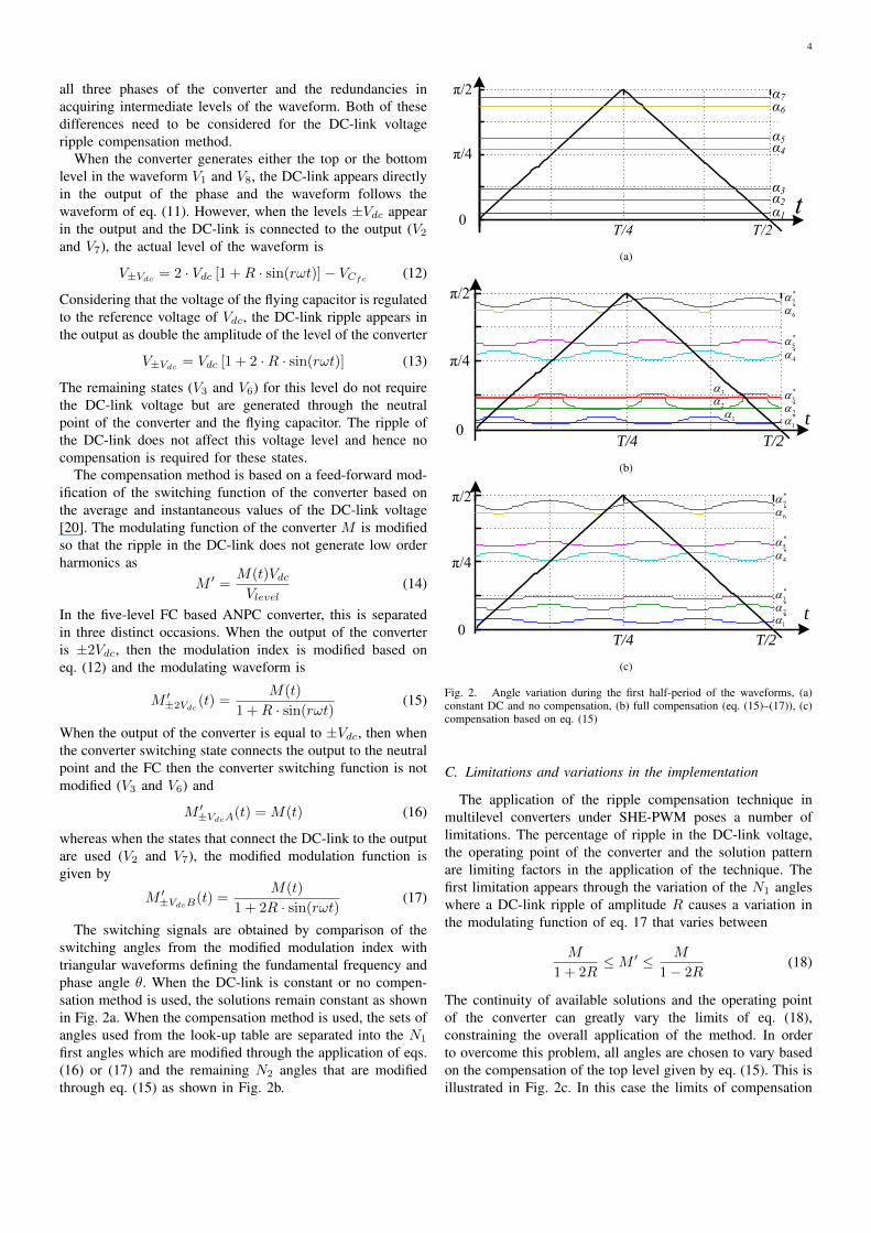
The switching signals are obtained by comparison of theswitching angles from the modified modulation index withtriangular waveforms defining the fundamental frequency andphase angle θ. When the DC-link is constant or no compen-sation method is used, the solutions remain constant as shownin Fig. 2a. When the compensation method is used, the sets ofangles used from the look-up table are separated into the N1
first angles which are modified through the application of eqs.(16) or (17) and the remaining N2 angles that are modifiedthrough eq. (15) as shown in Fig. 2b.
0
π/4
π/2
tα1α2α3
α4α5
α6α7
T/2T/4
(a)
0
π/4
π/2
t*11
2 *2
3 *3
4
*4*5
*6*7
T/2T/4(b)
0
π/4
π/2
tT/2T/4
*1*2*3
*4*5
*6*7
(c)
Fig. 2. Angle variation during the first half-period of the waveforms, (a)constant DC and no compensation, (b) full compensation (eq. (15)–(17)), (c)compensation based on eq. (15)
C. Limitations and variations in the implementation
The application of the ripple compensation technique inmultilevel converters under SHE-PWM poses a number oflimitations. The percentage of ripple in the DC-link voltage,the operating point of the converter and the solution patternare limiting factors in the application of the technique. Thefirst limitation appears through the variation of the N1 angleswhere a DC-link ripple of amplitude R causes a variation inthe modulating function of eq. 17 that varies between
M
1 + 2R≤M ′ ≤ M
1 − 2R(18)
The continuity of available solutions and the operating pointof the converter can greatly vary the limits of eq. (18),constraining the overall application of the method. In orderto overcome this problem, all angles are chosen to vary basedon the compensation of the top level given by eq. (15). This isillustrated in Fig. 2c. In this case the limits of compensation

5
1.3 1.4 1.5 1.60
10
20
30
40
50
60
70
80
90
M
Ang
les
in d
egre
es
α1
α2
α3
α4
α5α6
α7
Operating point under constant DC
Variation in the angles of the upper level
Variation in the angles of the lower level
(a)
1.3 1.4 1.5 1.60
10
20
30
40
50
60
70
80
90
M
Ang
les
in d
egre
es
α1
α2
α3
α4
α5α6
α7
Operating point under constant DC
Limits of operation with a maximum 5% ripple
Limits of operation with a maximum 10% ripple
(b)
Fig. 3. Limits of DC ripple compensation method, (a) full compensation,(b) modified compensation
areM
1 +R≤M ′ ≤ M
1 −R(19)
Outside these limits, the application of the method can nolonger fully compensate for the DC-link ripple and loworder harmonics will appear in the output. However, theseharmonics will be of much lower amplitude than in the caseof uncompensated waveforms.
The limits of the application are illustrated in Figs. 3a and3b. If we consider the operating point under constant DC-linkvoltage to be given by the solid line in both Figs. 3a andb, a ripple on the DC-link will result in a variation of theoperating point for the N1 and N2 angles as shown in Fig.3a and described by eqs. (15)–(17). As the lower angles N1
have a higher compensation factor, they reach the limits in thecontinuity of the solution earlier than the upper angles (N2).
The modification of the switching function as proposed ineq. (15), extends the operation of the compensation methodas shown in Fig. 3b. For the same operating point, theconverter can operate with 5% ripple and the limits are reachedwhen a harmonic component with approximately 10% for theparticular operating point of the converter, is present in theDC-link.
Additionally, when the waveform is switching between the±Vdc and ±2Vdc levels, the selection of angle modification
Vdc
ia
ib
ic
Lload Rload
Switching Angles look-up Table
Open / Closed loop controller
C1
C2
Eqs. (15), (16) and
(17)
VC1
VC2
++
Triangle wave
generator
Switching signals
θ SHE-PWMModulator
M
M'
dcVM
2'
dcVM
Level
Three-phase 5L ANPC
DC-link ripple compensator
Fig. 4. Simulation and experimental setup of the five-level ANPC converter
should be between eqs. (15), (16) and (17) as the DC-linkripple is involved in multiple ways. In order to reduce thecomplexity of the selection scheme and to avoid multipletransitions between the levels, the modification of eqn. (15)is only applied to the angles as shown in Fig. 2b. The anglemodification of eq. (15) lies always in between those ofeqs. (16) and (17) and presents a valid compromise betweenthe compensation requirements and the increased complexityof the selection scheme.
IV. SIMULATION RESULTS
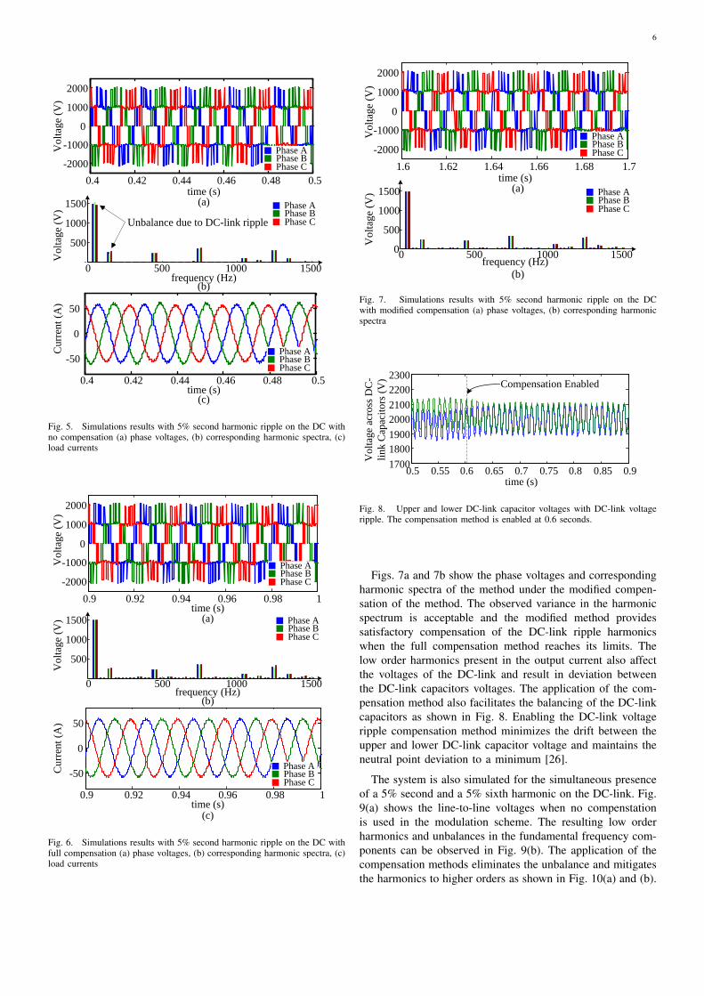
The DC link voltage ripple compensation method for thefive-level ANPC converter is simulated with MATLAB [27]and the PLECS toolbox [28]. A three-phase, five-level FCbased ANPC converter (Fig. 4) is simulated under a secondharmonic DC-link ripple with an amplitude equal to 5% of theDC-link voltage. The converter is initially simulated with theripple in the DC-link and without the compensation method inFig. 5a. The presence of the 2nd harmonic ripple generates loworder harmonics as well as a negative sequence fundamentalcomponent resulting in unbalanced output voltage waveforms.The harmonic spectrum of the output voltage is shown in Fig.5b and the phase currents of the converter are shown in Fig.5(c) where the unbalance in the currents caused by the DC-linkvoltage ripple can be observed.
The operation of the five-level ANPC under the DC-linkcompensation method is shown in Fig. 6. The angles aremodified based on the method of Section III-B with theswitching angles being modified as shown in Fig. 3a. Fig. 6ashows the output phase voltages and Fig. 6b the correspondingphase voltage harmonic spectra. The low order harmonicsas well as the unbalance due to the 2nd harmonic rippleon the DC-link are eliminated from the application of thecompensation method. The additional harmonics that appearin the spectra around the non-eliminated harmonics are dueto the modification of the switching angles from the methodwhich slightly modifies the quarter-wave symmetry assumedin the waveform formulation. The phase currents are given inFig. 6(c).
6
0.4 0.42 0.44 0.46 0.48 0.5
-2000
-1000
0
1000
2000
time (s)
Vol
tage
(V
)
0 500 1000 1500
500
1000
1500
frequency (Hz)
Vol
tage
(V
)
0.4 0.42 0.44 0.46 0.48 0.5
-50
0
50
time (s)
Cur
rent
(A
)
(b)
(c)
(a)
Unbalance due to DC-link ripple
Phase APhase BPhase C
Phase APhase BPhase C
Phase APhase BPhase C
Fig. 5. Simulations results with 5% second harmonic ripple on the DC withno compensation (a) phase voltages, (b) corresponding harmonic spectra, (c)load currents
0.9 0.92 0.94 0.96 0.98 1
-2000
-1000
0
1000
2000
time (s)
Vol
tage
(V
)
0 500 1000 1500
500
1000
1500
frequency (Hz)
Vol
tage
(V
)
0.9 0.92 0.94 0.96 0.98 1
-50
0
50
time (s)
Cur
rent
(A
)
(b)
(c)
(a)
Phase APhase BPhase C
Phase APhase BPhase C
Phase APhase BPhase C
Fig. 6. Simulations results with 5% second harmonic ripple on the DC withfull compensation (a) phase voltages, (b) corresponding harmonic spectra, (c)load currents
1.6 1.62 1.64 1.66 1.68 1.7
-2000
-1000
0
1000
2000
time (s)
Vol
tage
(V
)
0 500 1000 15000
500
1000
1500
frequency (Hz)
Vol
tage
(V
)1.6 1.62 1.64 1.66 1.68 1.7
-50
0
50
time (s)C
urre
nt (
A)
(b)
(c)
(a)
Phase APhase BPhase C
Phase APhase BPhase C
Phase APhase BPhase C
Fig. 7. Simulations results with 5% second harmonic ripple on the DCwith modified compensation (a) phase voltages, (b) corresponding harmonicspectra
0.5 0.55 0.6 0.65 0.7 0.75 0.8 0.85 0.91700
18001900
20002100
22002300
time (s)
Vol
tage
acr
oss
DC
-li
nk C
apac
itors
(V
) Compensation Enabled
Fig. 8. Upper and lower DC-link capacitor voltages with DC-link voltageripple. The compensation method is enabled at 0.6 seconds.
Figs. 7a and 7b show the phase voltages and correspondingharmonic spectra of the method under the modified compen-sation of the method. The observed variance in the harmonicspectrum is acceptable and the modified method providessatisfactory compensation of the DC-link ripple harmonicswhen the full compensation method reaches its limits. Thelow order harmonics present in the output current also affectthe voltages of the DC-link and result in deviation betweenthe DC-link capacitors voltages. The application of the com-pensation method also facilitates the balancing of the DC-linkcapacitors as shown in Fig. 8. Enabling the DC-link voltageripple compensation method minimizes the drift between theupper and lower DC-link capacitor voltage and maintains theneutral point deviation to a minimum [26].
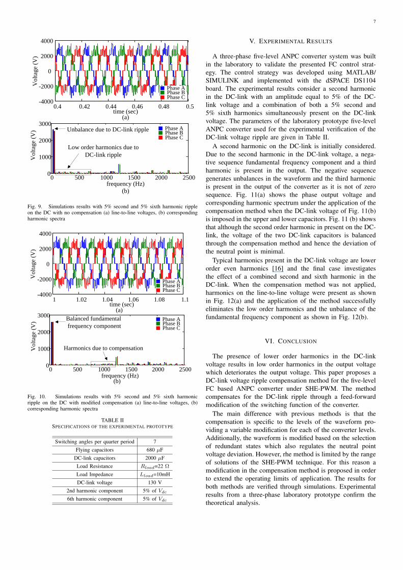
The system is also simulated for the simultaneous presenceof a 5% second and a 5% sixth harmonic on the DC-link. Fig.9(a) shows the line-to-line voltages when no compenstationis used in the modulation scheme. The resulting low orderharmonics and unbalances in the fundamental frequency com-ponents can be observed in Fig. 9(b). The application of thecompensation methods eliminates the unbalance and mitigatesthe harmonics to higher orders as shown in Fig. 10(a) and (b).
7
0.4 0.42 0.44 0.46 0.48 0.5-4000
-2000
0
2000
4000
time (sec)
Vol
tage
(V
)
0 500 1000 1500 2000 25000
1000
2000
3000
frequency (Hz)
Vol
tage
(V
)
(a)
Unbalance due to DC-link ripple
Phase APhase BPhase C
Phase APhase BPhase C
Low order harmonics due to DC-link ripple
(b)
Fig. 9. Simulations results with 5% second and 5% sixth harmonic rippleon the DC with no compensation (a) line-to-line voltages, (b) correspondingharmonic spectra
1 1.02 1.04 1.06 1.08 1.1-4000
-2000
0
2000
4000
time (sec)
Vol
tage
(V
)
0 500 1000 1500 2000 25000
1000
2000
3000
frequency (Hz)
Vol
tage
(V
)
(a)
(b)
Phase APhase BPhase C
Phase APhase BPhase C
Harmonics due to compensation
Balanced fundamentalfrequency component
Fig. 10. Simulations results with 5% second and 5% sixth harmonicripple on the DC with modified compensation (a) line-to-line voltages, (b)corresponding harmonic spectra
TABLE IISPECIFICATIONS OF THE EXPERIMENTAL PROTOTYPE
Switching angles per quarter period 7
Flying capacitors 680 µF
DC-link capacitors 2000 µF
Load Resistance Rload=22 Ω
Load Impedance Lload=10mH
DC-link voltage 130 V
2nd harmonic component 5% of Vdc6th harmonic component 5% of Vdc
V. EXPERIMENTAL RESULTS
A three-phase five-level ANPC converter system was builtin the laboratory to validate the presented FC control strat-egy. The control strategy was developed using MATLAB/SIMULINK and implemented with the dSPACE DS1104board. The experimental results consider a second harmonicin the DC-link with an amplitude equal to 5% of the DC-link voltage and a combination of both a 5% second and5% sixth harmonics simultaneously present on the DC-linkvoltage. The parameters of the laboratory prototype five-levelANPC converter used for the experimental verification of theDC-link voltage ripple are given in Table II.
A second harmonic on the DC-link is initially considered.Due to the second harmonic in the DC-link voltage, a nega-tive sequence fundamental frequency component and a thirdharmonic is present in the output. The negative sequencegenerates unbalances in the waveform and the third harmonicis present in the output of the converter as it is not of zerosequence. Fig. 11(a) shows the phase output voltage andcorresponding harmonic spectrum under the application of thecompensation method when the DC-link voltage of Fig. 11(b)is imposed in the upper and lower capacitors. Fig. 11 (b) showsthat although the second order harmonic in present on the DC-link, the voltage of the two DC-link capacitors is balancedthrough the compensation method and hence the deviation ofthe neutral point is minimal.
Typical harmonics present in the DC-link voltage are lowerorder even harmonics [16] and the final case investigatesthe effect of a combined second and sixth harmonic in theDC-link. When the compensation method was not applied,harmonics on the line-to-line voltage were present as shownin Fig. 12(a) and the application of the method successfullyeliminates the low order harmonics and the unbalance of thefundamental frequency component as shown in Fig. 12(b).
VI. CONCLUSION
The presence of lower order harmonics in the DC-linkvoltage results in low order harmonics in the output voltagewhich deteriorates the output voltage. This paper proposes aDC-link voltage ripple compensation method for the five-levelFC based ANPC converter under SHE-PWM. The methodcompensates for the DC-link ripple through a feed-forwardmodification of the switching function of the converter.
The main difference with previous methods is that thecompensation is specific to the levels of the waveform pro-viding a variable modification for each of the converter levels.Additionally, the waveform is modified based on the selectionof redundant states which also regulates the neutral pointvoltage deviation. However, rhe method is limited by the rangeof solutions of the SHE-PWM technique. For this reason amodification in the compensation method is proposed in orderto extend the operating limits of application. The results forboth methods are verified through simulations. Experimentalresults from a three-phase laboratory prototype confirm thetheoretical analysis.

8
Harmonics due to voltageripple compensation
(a)
(b)
Load current
Capacitor current
Capacitor voltage ripple
(c)
Fig. 11. Experimental results with 10% second harmonic ripple in DC-link voltage and compensation, (a) Phase voltage and associated harmonicspectrum, (b) upper and lower DC-link capacitor voltages, (c) output current(Channel2), current through FC (Channel4), and voltage ripple across the FC(Channel3)
APPENDIX A
The following table summarizes all the abbrevations usedin this paper.
5th 7th3rd 23rdHarmonics due to DC-link ripple
(a)
23rd17th 21st
Harmonics due to compensation
(b)
Fig. 12. Experimental results with 5% second and 5% sixth harmonic. Line-to-line voltages (a) without compensation (b) with compensation
Abbreviation Term
ANPC Active Neutral Point ClampedCHB Cascaded H-bridgesCTL Cascaded Two LevelFC Flying Capacitor
LSC Level Shifted CarriersM2LC Modular Multilevel ConverterPSC Phase Shifted Carriers
PWM Pulse Width ModulationSF Switching Function
SHE Selective Harmonic EliminationSVM Space Vector ModulationVSC Voltage Source Converter
REFERENCES
[1] N. Flourentzou, V. G. Agelidis, and G. Demetriades, “VSC based HVDCpower transmission systems: An overview,” in IEEE Trans. on PowerElectron., vol. 24, no. 3, pp. 592–602, 2009.
[2] M. Glinka and R. Marquardt, “A new AC/AC multilevel converter family,”
9
in IEEE Transactions on Industrial Electronics, Vol. 52, No. 3, 2005, pp.662–669.
[3] B. Jacobsohn, P. Karlsson, G. Asplund, L. Harnefors, T. Johsson, “VSC-HVDC Transmission with cascaded two-level converters,” in CIGRE2010, paper B4-110
[4] S. Kouro, M. Malinowski, K. Gopakumar, J.Pou, L. G. Franquelo, B.Wu,J. Rodriguez, M. A. Perez, and J. I. Leon, “Recent advances and industrialapplications of multilevel converters,” IEEE Trans. on Ind. Electron., vol.57, no. 8, pp. 2553-2580, Aug. 2010
[5] A. Lopez-de-Heredia, H. Gaztanaga, U. Viscarret, I. Etxeberria-Otadui, L.Aldasoro, and T. Nieva, “Comparison of H-NPC and parallel-H topologiesfor an AC traction front-end converters,” in Proc. of EPE, 2009, pp.1-9.
[6] M. Veenstra and A. Rufer, “Control of a hybrid asymmetric multilevelinverter for competitive medium-voltage industrial drives,” in IEEETrans.on Ind. Appl., vol. 41, no.2, pp.655-664, Mar./Apr. 2005.
[7] T. Bruckner, S. Bernet, and H. Guldner “The active NPC converter andits loss-balancing control,” in IEEE Trans. on Ind. Electron., vol. 52, no.3, pp. 855-868, Jun. 2005.
[8] S. R. Pulikanti, G. Konstantinou, and V. G. Agelidis, “Seven-levelcascaded ANPC-based multilevel converter,” in Proc. of IEEE ECCE,2010, pp. 4575-4582.
[9] P. Barbosa, M. Saeedifard, P. K. Steimer, and C. Haederil, “Space vectormodulation control of a seven-level hybrid converter,” in Proc. of IEEEPESC, 2008, pp. 4487-4493.
[10] P. Barbosa, P. K. Steimer, M. Winkelnkemper, J. Steinke, and N.Celanovic, “Active-neutral-point clamped (ANPC) multilevel convertertechnology,” in Proc. of EPE Conf., 2005, pp.11-14.
[11] F. Kieferndorf, M. Basler, L. A. Serpa, J. H. Fabian, A. Coccia, and G.A. Scheuer, ”A new medium voltage drive system based on ANPC-5Ltechnology,” in Proc. of ICIT Conf., 2010, pp.605-611.
[12] S. A. Gonzalez, M. I. Valla, and C.F. Christiansen, “Five-level cascadedasymmetric multilevel converter,” in IET Power Electron., vol. 3, no. 1,pp. 120-128, 2010.
[13] S. R. Pulikanti, G. Konstantinou, and V. G. Agelidis “An n-level flyingcapacitor based active neutral point clamped converter,” in Proc. of IEEEPEDG, 2010, pp.553-558.
[14] S.R. Pulikanti, G. Konstantinou, V.G. Agelidis, “Generalization offlying-capacitor based active-neutral-point-clamped Multilevel ConverterUsing Voltage-Level Modulation” in IET Power Electronics, Vol. 5, No.4, pp. 456–466, May 2012.
[15] S. R. Pulikanti and V. G. Agelidis, “Hybrid flying capacitor based active-neutral-point-clamped five-level converter operated with SHE-PWM,” inIEEE Trans. on Ind. Electr., vol. 58, no.10, Oct 2011, pp 4643–4653.
[16] S. Kouro, P. Lezana, M. Angulo, and J. Rodriguez, “Multicarrier PWMwith DC-link ripple feedforward compensation for multilevel inverters,”in IEEE Trans. on Power Electron., vol. 23, no. 1, pp. 52-59, Jan. 2008.
[17] F. Blaabjerg, J. K. Pedersen, and P. Thogersen, “Improved modulationtechniques for PWM-VSI drives,” in Proc. IECON, 1993, pp. 1187-1192.
[18] K. Smedley and S. Cuk, “One-cycle control of switching converters,” inIEEE Trans. Power Electron., vol. 10, no. 6, pp. 625-633, Nov. 1995.
[19] J. Vodden, P. Wheeler, and J, Clare, “DC link balancing and ripplecompensation for a cascaded-H-bridge using space vector modulation,”in Proc. of IEEE ECCE, 2009, pp. 3093-3099.
[20] P. N. Enjeti and W. Shireen, “A new technique to reject DC-link voltageripple for inverters operating on programmed PWM waveforms,” in IEEETrans. on Power Electron., vol. 7, no. 1, pp. 171-180, Jan. 1992.
[21] N. Flourentzou and V. G. Agelidis, “Optimized modulation for AC-DCharmonic immunity in VSC-HVDC transmission,” in IEEE Trans. PowerDel., vol. 25, no. 3, pp. 1713-1720, Jul. 2010.
[22] P. M. Bhagwat and V. R. Stefanovic, “Generalized structure of amultilevel PWM inverter”, in IEEE Trans. on Ind. Appl., vol. IA-19, no6, pp. 1057-1069, Nov./Dec. 1983.
[23] V. G. Agelidis, A. Balouktsis, and M. S. A. Dahidah, “A five-levelsymmetrically defined selective harmonic elimination PWM strategy:analysis and experimental validation”, in IEEE Trans. on Power Electron.,vol. 23, no 1, pp.19-26, Jan. 2008.
[24] M. S. A. Dahidah and V. G. Agelidis, “Selective harmonic eliminationPWM control for cascaded multilevel voltage source converters: a gener-alized formula”, in IEEE Trans. on Power Electron., vol. 23, no. 4, pp.1620-1630, Jul. 2008.
[25] L. Xu and V. G. Agelidis, “VSC transmission system using flyingcapacitor multilevel converters and hybrid PWM control,” in IEEE Trans.Power Delivery, vol. 22, no. 1, pp. 693-702, Jan. 2007.
[26] S. R. Pulikanti, M. S. A. Dahidah, and V. G. Agelidis, “Voltage balancingcontrol of three-level active NPC converter using SHE-PWM,” in IEEETrans. Power Del., Vol. 26, No. 1, pp. 258–267, Jan. 2011.
[27] MATLAB/SIMULINK software package, version R2007a, The MathWorks, http://www.mathworks.com
[28] PLECS 3.2.3, http://www.plexim.com
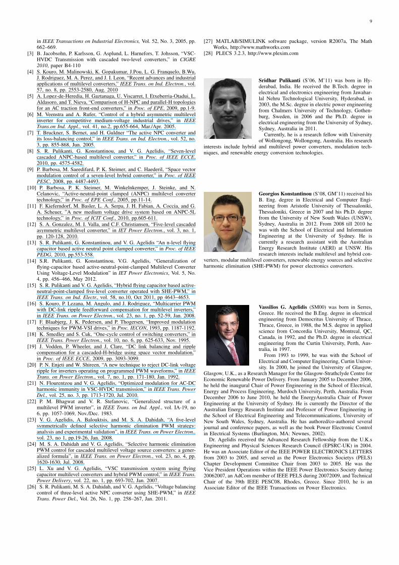
Sridhar Pulikanti (S’06, M’11) was born in Hy-derabad, India. He received the B.Tech. degree inelectrical and electronics engineering from Jawahar-lal Nehru Technological University, Hyderabad, in2003, the M.Sc. degree in electric power engineeringfrom Chalmers University of Technology, Gothen-burg, Sweden, in 2006 and the Ph.D. degree inelectrical engineering from the University of Sydney,Sydney, Australia in 2011.
Currently, he is a research fellow with Universityof Wollongong, Wollongong, Australia. His research
interests include hybrid and multilevel power converters, modulation tech-niques, and renewable energy conversion technologies.
Georgios Konstantinou (S’08, GM’11) received hisB. Eng. degree in Electrical and Computer Engi-neering from Aristotle University of Thessaloniki,Thessaloniki, Greece in 2007 and his Ph.D. degreefrom the University of New South Wales (UNSW),Sydney, Australia in 2012. From 2008 till 2010 hewas with the School of Electrical and InformationEngineering at the University of Sydney. He iscurrently a research assistant with the AustralianEnergy Research Institute (AERI) at UNSW. Hisresearch interests include multilevel and hybrid con-
verters, modular multilevel converters, renewable energy sources and selectiveharmonic elimination (SHE-PWM) for power electronics converters.
Vassilios G. Agelidis (SM00) was born in Serres,Greece. He received the B.Eng. degree in electricalengineering from Democritus University of Thrace,Thrace, Greece, in 1988, the M.S. degree in appliedscience from Concordia University, Montreal, QC,Canada, in 1992, and the Ph.D. degree in electricalengineering from the Curtin University, Perth, Aus-tralia, in 1997.
From 1993 to 1999, he was with the School ofElectrical and Computer Engineering, Curtin Univer-sity. In 2000, he joined the University of Glasgow,
Glasgow, U.K., as a Research Manager for the Glasgow-Strathclyde Centre forEconomic Renewable Power Delivery. From January 2005 to December 2006,he held the inaugural Chair of Power Engineering in the School of Electrical,Energy and Process Engineering, Murdoch University, Perth, Australia. FromDecember 2006 to June 2010, he held the EnergyAustralia Chair of PowerEngineering at the University of Sydney. He is currently the Director of theAustralian Energy Research Institute and Professor of Power Engineering inthe School of Electrical Engineering and Telecommunications, University ofNew South Wales, Sydney, Australia. He has authored/co-authored severaljournal and conference papers, as well as the book Power Electronic Controlin Electrical Systems (Burlington, MA: Newnes, 2002).
Dr. Agelidis received the Advanced Research Fellowship from the U.K.sEngineering and Physical Sciences Research Council (EPSRC-UK) in 2004.He was an Associate Editor of the IEEE POWER ELECTRONICS LETTERSfrom 2003 to 2005, and served as the Power Electronics Societys (PELS)Chapter Development Committee Chair from 2003 to 2005. He was theVice President Operations within the IEEE Power Electronics Society during20062007, an AdCom member of IEEE PELS during 20072009, and TechnicalChair of the 39th IEEE PESC08, Rhodes, Greece. Since 2010, he is anAssociate Editor of the IEEE Transactions on Power Electronics.
Copyright © 2022 FDOKUMEN