tl1454a, tl1454ay dual channel pulse width modulation (pwm ...
26
TL1454A, TL1454AY DUALĆCHANNEL PULSEĆWIDTHĆMODULATION (PWM) CONTROL CIRCUIT SLVS423 A- MAY 2002 - REVISED SEPTEMBER 2002 1 POST OFFICE BOX 655303 • DALLAS, TEXAS 75265 D Two Complete PWM Control Circuits D Outputs Drive MOSFETs Directly D Oscillator Frequency . . . 50 kHz to 2 MHz D 3.6-V to 20-V Supply-Voltage Range D Low Supply Current . . . 3.5 mA Typ D Adjustable Dead-Time Control, 0% to 100% D 1.26-V Reference description The TL1454A is a dual-channel pulse-width-mod- ulation (PWM) control circuit, primarily intended for low-power, dc/dc converters. Applications include LCD displays, backlight inverters, note- book computers, and other products requiring small, high-frequency, dc/dc converters. Each PWM channel has its own error amplifier, PWM comparator, dead-time control comparator, and MOSFET driver. The voltage reference, oscillator, undervoltage lockout, and short-circuit protection are common to both channels. Channel 1 is configured to drive n-channel MOSFETs in step-up or flyback converters, and channel 2 is configured to drive p-channel MOSFETs in step-down or inverting converters. The operating frequency is set with an external resistor and an external capacitor, and dead time is continuously adjustable from 0 to 100% duty cycle with a resistive divider network. Soft start can be implemented by adding a capacitor to the dead-time control (DTC) network. The error-amplifier common-mode input range includes ground, which allows the TL1454A to be used in ground-sensing battery chargers as well as voltage converters. AVAILABLE OPTIONS PACKAGED DEVICES † CHIP FORM T A SMALL OUTLINE (D) PLASTIC DIP (N) TSSOP (PW) SSOP (DB) SOP-EIAJ (NS) CHIP FORM (Y) -20°C to 85°C TL1454ACD TL1454ACN TL1454ACPWR TL1454ACDB TL1454ACNS TL1454AY † The D, DB and NS packages are available taped and reeled. Add the suffix R to the device name (e.g., TL1454ACDR). The PW package is available only left-end taped and reeled (indicated by the R suffix on the device type; e.g., TL1454ACPWR). Copyright 2002, Texas Instruments Incorporated PRODUCTION DATA information is current as of publication date. Products conform to specifications per the terms of Texas Instruments standard warranty. Production processing does not necessarily include testing of all parameters. 1 2 3 4 5 6 7 8 16 15 14 13 12 11 10 9 CT RT DTC1 IN1+ IN1- COMP1 GND OUT1 D, N OR PW PACKAGE (TOP VIEW) REF SCP DTC2 IN2+ IN2- COMP2 V CC OUT2
-
Upload
khangminh22 -
Category
Documents
-
view
3 -
download
0
Transcript of tl1454a, tl1454ay dual channel pulse width modulation (pwm ...

SLVS423 A− MAY 2002 − REVISED SEPTEMBER 2002
1POST OFFICE BOX 655303 • DALLAS, TEXAS 75265
Two Complete PWM Control Circuits
Outputs Drive MOSFETs Directly
Oscillator Frequenc y . . . 50 kHz to 2 MHz
3.6-V to 20-V Supply-Voltage Range
Low Supply Current . . . 3.5 mA Typ
Adjustable Dead-Time Control, 0% to 100%
1.26-V Reference
description
The TL1454A is a dual-channel pulse-width-mod-ulation (PWM) control circuit, primarily intendedfor low-power, dc/dc converters. Applicationsinclude LCD displays, backlight inverters, note-book computers, and other products requiringsmall, high-frequency, dc/dc converters.
Each PWM channel has its own error amplifier, PWM comparator, dead-time control comparator, and MOSFETdriver. The voltage reference, oscillator, undervoltage lockout, and short-circuit protection are common to bothchannels.
Channel 1 is configured to drive n-channel MOSFETs in step-up or flyback converters, and channel 2 isconfigured to drive p-channel MOSFETs in step-down or inverting converters. The operating frequency is setwith an external resistor and an external capacitor, and dead time is continuously adjustable from 0 to 100%duty cycle with a resistive divider network. Soft start can be implemented by adding a capacitor to the dead-timecontrol (DTC) network. The error-amplifier common-mode input range includes ground, which allows theTL1454A to be used in ground-sensing battery chargers as well as voltage converters.
AVAILABLE OPTIONS
PACKAGED DEVICES †CHIP FORM
TA SMALL OUTLINE(D)
PLASTIC DIP(N)
TSSOP(PW)
SSOP(DB)
SOP-EIAJ(NS)
CHIP FORM(Y)
−20°C to 85°C TL1454ACD TL1454ACN TL1454ACPWR TL1454ACDB TL1454ACNS TL1454AY† The D, DB and NS packages are available taped and reeled. Add the suffix R to the device name (e.g., TL1454ACDR). The PW package is
available only left-end taped and reeled (indicated by the R suffix on the device type; e.g., TL1454ACPWR).
Copyright 2002, Texas Instruments Incorporated ! " #$%! " &$'(#! )!%*)$#!" # ! "&%##!" &% !+% !%" %," "!$%!""!)) -!.* )$#! &#%""/ )%" ! %#%""(. #($)%!%"!/ (( &%!%"*
1
2
3
4
5
6
7
8
16
15
14
13
12
11
10
9
CTRT
DTC1IN1+IN1−
COMP1GND
OUT1
D, N OR PW PACKAGE(TOP VIEW)
REFSCPDTC2IN2+IN2−COMP2VCCOUT2

SLVS423 A− MAY 2002 − REVISED SEPTEMBER 2002
2 POST OFFICE BOX 655303 • DALLAS, TEXAS 75265
functional block diagram
_+
_+
OSCPWM
Comparator 1
ErrorAmplifier 1
To InternalCircuitry
2.5 V
1.26 V
1 V1 V
SCP
VCC
GND
DTC1 DTC2
14315
7
16
4
5
13
12
6
11
10 2 1CTRT
OUT1
OUT2
8
VCC
UVLOand
SCP Latch
IN1+
IN1−
IN2+
IN2−
COMP1
COMP2
REF1.8 V
1.2 V
SCPComparator 1
VoltageREF
9
VCC
0.65 V0.65 V
1.27 V
PWMComparator 2
ErrorAmplifier 2
SCPComparator 2
SLVS423 A− MAY 2002 − REVISED SEPTEMBER 2002
3POST OFFICE BOX 655303 • DALLAS, TEXAS 75265
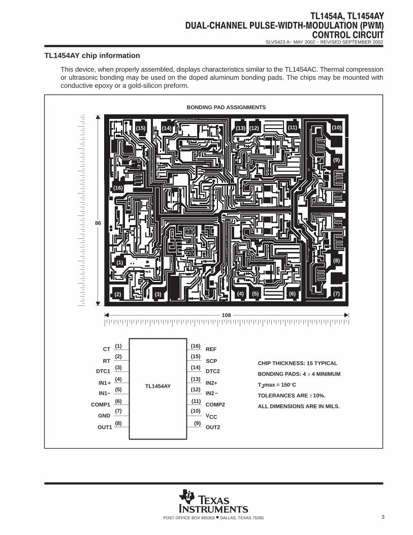
TL1454AY chip information
This device, when properly assembled, displays characteristics similar to the TL1454AC. Thermal compressionor ultrasonic bonding may be used on the doped aluminum bonding pads. The chips may be mounted withconductive epoxy or a gold-silicon preform.
BONDING PAD ASSIGNMENTS
CHIP THICKNESS: 15 TYPICAL
BONDING PADS: 4 × 4 MINIMUM
TJmax = 150°C
TOLERANCES ARE ±10%.
ALL DIMENSIONS ARE IN MILS.
TL1454AY
(2)
(14)
(1)
(3)
(4)
(5)
(6)
(7)
(8)
(16)
(13)
(12)
(11)
(10)
(9)
REF
DTC2
IN2+
IN2−
COMP2
VCC
OUT2OUT1
COMP1
IN1−
IN1+
RT
CT
GND
86
108
(1)
(2) (3) (4) (5) (6) (7)
(10)(11)(12)(13)(14)(15)
(16)
(8)
(9)
(15)SCP
DTC1

SLVS423 A− MAY 2002 − REVISED SEPTEMBER 2002
4 POST OFFICE BOX 655303 • DALLAS, TEXAS 75265
theory of operation
reference voltage
A linear regulator operating from VCC generates a 2.5-V supply for the internal circuits and the 1.26-V reference,which can source a maximum of 1 mA for external loads. A small ceramic capacitor (0.047 µF to 0.1 µF) betweenREF and ground is recommended to minimize noise pickup.
error amplifier
The error amplifier generates the error signal used by the PWM to adjust the power-switch duty cycle for thedesired converter output voltage. The signal is generated by comparing a sample of the output voltage to thevoltage reference and amplifying the difference. An external resistive divider connected between the converteroutput and ground, as shown in Figure 1, is generally required to obtain the output voltage sample.
The amplifier output is brought out on COMP to allow the frequency response of the amplifier to be shaped withan external RC network to stabilize the feedback loop of the converter. DC loading on the COMP output is limitedto 45 µA (the maximum amplifier source current capability).
Figure 1 illustrates the sense-divider network and error-amplifier connections for converters with positive outputvoltages. The divider network is connected to the noninverting amplifier input because the PWM has a phaseinversion; the duty cycle decreases as the error-amplifier output increases.
_
+
IN−
IN+
R3
R1R2
COMP
To PWMVO
CompensationNetwork
REF
ConverterOutput
TL1454A
Figure 1. Sense Divider/Error Amplifier Configuration for Converters with Positive Outputs
The output voltage is given by:
VO Vref1 R1
R2
where Vref = 1.26 V.
The dc source resistance of the error-amplifier inputs should be 10 kΩ or less and approximately matched tominimize output voltage errors caused by the input-bias current. A simple procedure for determining appropriatevalues for the resistors is to choose a convenient value for R3 (10 kΩ or less) and calculate R1 and R2 using:
R1 R3VO
VO–Vref
R2 R3VOVref
SLVS423 A− MAY 2002 − REVISED SEPTEMBER 2002
5POST OFFICE BOX 655303 • DALLAS, TEXAS 75265
error amplifier
R1 and R2 should be tight-tolerance (±1% or better) devices with low and/or matched temperature coefficientsto minimize output voltage errors. A device with a ±5% tolerance is suitable for R3.
_
+
IN−
IN+
R2
COMP
To PWM
VO
CompensationNetwork
REF
R1R3
ConverterOutput
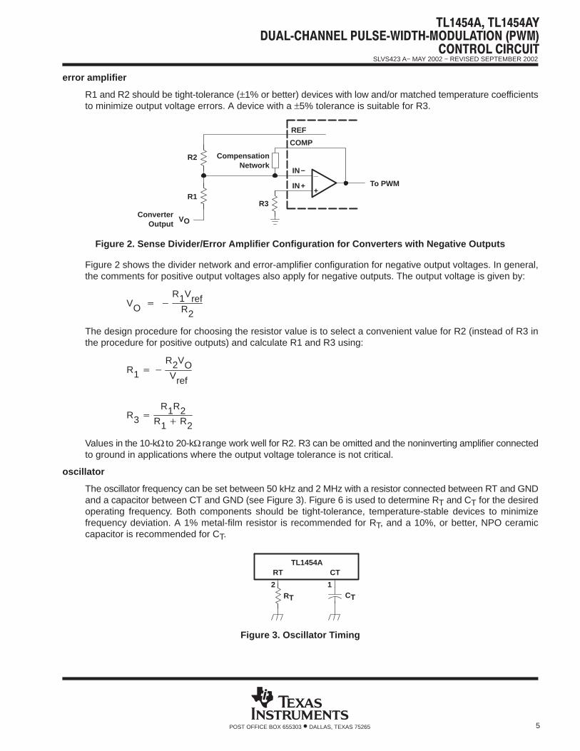
Figure 2. Sense Divider/Error Amplifier Configuration for Converters with Negative Outputs
Figure 2 shows the divider network and error-amplifier configuration for negative output voltages. In general,the comments for positive output voltages also apply for negative outputs. The output voltage is given by:
VO R1Vref
R2
The design procedure for choosing the resistor value is to select a convenient value for R2 (instead of R3 inthe procedure for positive outputs) and calculate R1 and R3 using:
R1 R2VOVref
R3 R1R2
R1 R2
Values in the 10-kΩ to 20-kΩ range work well for R2. R3 can be omitted and the noninverting amplifier connectedto ground in applications where the output voltage tolerance is not critical.
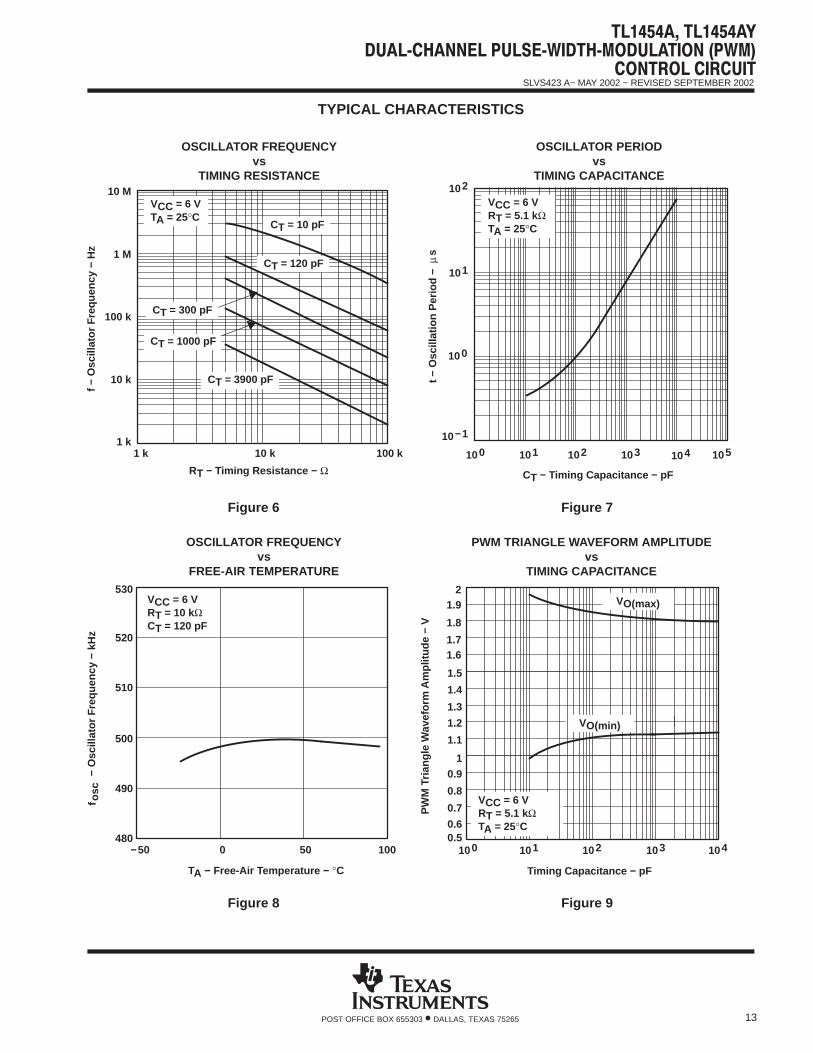
oscillator
The oscillator frequency can be set between 50 kHz and 2 MHz with a resistor connected between RT and GNDand a capacitor between CT and GND (see Figure 3). Figure 6 is used to determine RT and CT for the desiredoperating frequency. Both components should be tight-tolerance, temperature-stable devices to minimizefrequency deviation. A 1% metal-film resistor is recommended for RT, and a 10%, or better, NPO ceramiccapacitor is recommended for CT.
RT CT
RT CTTL1454A
2 1
Figure 3. Oscillator Timing

SLVS423 A− MAY 2002 − REVISED SEPTEMBER 2002
6 POST OFFICE BOX 655303 • DALLAS, TEXAS 75265
dead-time control (DTC) and soft start
The two PWM channels have independent dead-time control inputs so that the maximum power-switch dutycycles can be limited to less then 100%. The dead-time is set with a voltage applied to DTC; the voltage istypically obtained from a resistive divider connected between the reference and ground as shown in Figure 4.Soft start is implemented by adding a capacitor between REF and DTC.
The voltage, VDT, required to limit the duty cycle to a maximum value is given by:
VDT VO(max) DVO(max) VO(min) 0.65
where VO(max) and VO(min) are obtained from Figure 9, and D is the maximum duty cycle.
Predicting the regulator startup or rise time is complicated because it depends on many variables, including:input voltage, output voltage, filter values, converter topology, and operating frequency. In general, the outputwill be in regulation within two time constants of the soft-start circuit. A five-to-ten millisecond time constantusually works well for low-power converters.
The DTC input can be grounded in applications where achieving a 100% duty cycle is desirable, such as a buckconverter with a very low input-to-output differential voltage. However, grounding DTC prevents theimplementation of soft start, and the output voltage overshoot at power-on is likely to be very large. A betterarrangement is to omit RDT1 (see Figure 4) and choose RDT2 = 47 kΩ. This configuration ensures that the dutycycle can reach 100% and still allows the designer to implement soft start using CSS.
CSS
REF
TL1454ARDT1DTC
RDT2
16
Figure 4. Dead-Time Control and Soft Start
PWM comparator
Each of the PWM comparators has dual inverting inputs. One inverting input is connected to the output of theerror amplifier; the other inverting input is connected to the DTC terminal. Under normal operating conditions,when either the error-amplifier output or the dead-time control voltage is higher than that for the PWM trianglewave, the output stage is set inactive (OUT1 low and OUT2 high), turning the external power stage off.
undervoltage-lockout (UVLO) protection
The undervoltage-lockout circuit turns the output circuit off and resets the SCP latch whenever the supplyvoltage drops too low (to approximately 2.9 V) for proper operation. A hysteresis voltage of 200 mV eliminatesfalse triggering on noise and chattering.
short-circuit protection (SCP)
The TL1454A SCP function prevents damage to the power switches when the converter output is shorted toground. In normal operation, SCP comparator 1 clamps SCP to approximately 185 mV. When one of theconverter outputs is shorted, the error amplifier output (COMP) will be driven below 1 V to maximize duty cycleand force the converter output back up. When the error amplifier output drops below 1 V, SCP comparator 1releases SCP, and capacitor, CSCP, which is connected between SCP and GND, begins charging. If theerror-amplifier output rises above 1 V before CSCP is charged to 1 V, SCP comparator 1 discharges CSCP andnormal operation resumes. If CSCP reaches 1 V, SCP comparator 2 turns on and sets the SCP latch, which turnsoff the output drives and resets the soft-start circuit. The latch remains set until the supply voltage is loweredto 2 V or less, or CSCP is discharged externally.

SLVS423 A− MAY 2002 − REVISED SEPTEMBER 2002
7POST OFFICE BOX 655303 • DALLAS, TEXAS 75265
short-circuit protection (SCP) (continued)
The SCP time-out period must be greater than the converter start-up time or the converter will not start. Becausehigh-value capacitor tolerances tend to be ±20% or more and IC resistor tolerances are loose as well, it is bestto choose an SCP time-out period 10-to-15 times greater than the converter startup time. The value of CSCPmay be determined using Figure 6, or it can be calculated using:
CSCP TSCP80.3
where CSCP is in µF and TSCP is the time-out period in ms.
output stage
The output stage of the TL1454A is a totem-pole output with a maximum source/sink current rating of 40 mAand a voltage rating of 20 V. The output is controlled by a complementary output AND gate and is turned on(sourcing current for OUT1, sinking current for OUT2) when all the following conditions are met: 1) the oscillatortriangle wave voltage is higher than both the DTC voltage and the error-amplifier output voltage, 2) theundervoltage-lockout circuit is inactive, and 3) the short-circuit protection circuit is inactive.
absolute maximum ratings over operating free-air temperature range (unless otherwise noted) †
Supply voltage, VCC (see Note 1) 23 V. . . . . . . . . . . . . . . . . . . . . . . . . . . . . . . . . . . . . . . . . . . . . . . . . . . . . . . . . . . . Error amplifier input voltage: IN1+, IN1−, IN2+, IN2− 23 V. . . . . . . . . . . . . . . . . . . . . . . . . . . . . . . . . . . . . . . . . . . . Output voltage: OUT1, OUT2 20 V. . . . . . . . . . . . . . . . . . . . . . . . . . . . . . . . . . . . . . . . . . . . . . . . . . . . . . . . . . . . . . . . Continuous output current: OUT1, OUT2 ±200 mA. . . . . . . . . . . . . . . . . . . . . . . . . . . . . . . . . . . . . . . . . . . . . . . . . . Peak output current: OUT1, OUT2 1 A. . . . . . . . . . . . . . . . . . . . . . . . . . . . . . . . . . . . . . . . . . . . . . . . . . . . . . . . . . . . Continuous total dissipation See Dissipation Rating Table. . . . . . . . . . . . . . . . . . . . . . . . . . . . . . . . . . . . . . . . . . . Operating free-air temperature range, TA: C suffix −20°C to 85°C. . . . . . . . . . . . . . . . . . . . . . . . . . . . . . . . . . . . Storage temperature range, Tstg −65°C to 150°C. . . . . . . . . . . . . . . . . . . . . . . . . . . . . . . . . . . . . . . . . . . . . . . . . . . Lead temperature 1,6 mm (1/16 inch) from case for 10 seconds 260°C. . . . . . . . . . . . . . . . . . . . . . . . . . . . . . .
† Stresses beyond those listed under “absolute maximum ratings” may cause permanent damage to the device. These are stress ratings only, andfunctional operation of the device at these or any other conditions beyond those indicated under “recommended operating conditions” is notimplied. Exposure to absolute-maximum-rated conditions for extended periods may affect device reliability.
NOTE 1: All voltage values are with respect to network GND.
DISSIPATION RATING TABLE
PACKAGETA ≤ 25°C
POWER RATINGDERATING FACTORABOVE TA = 25°C
TA = 70°CPOWER RATING
TA = 85°CPOWER RATING
D 950 mW 7.6 mW/°C 608 mW 494 mW
DB 1000 mW 8.0 mW/°C 640 mW 520 mW
N 1250 mW 10.0 mW/°C 800 mW 650 mW
NS 1953 mW 15.6 mW/°C 1250 mW 1015 mW
PW 500 mW 4.0 mW/°C 320 mW 260 mW

SLVS423 A− MAY 2002 − REVISED SEPTEMBER 2002
8 POST OFFICE BOX 655303 • DALLAS, TEXAS 75265
recommended operating conditionsMIN MAX UNIT
Supply voltage, VCC 3.6 20 V
Error amplifier common-mode input voltage −0.2 1.45 V
Output voltage, VO 20 V
Output current, IO ±40 mA
COMP source current −45 µA
COMP sink current 100 µA
Reference output current 1 mA
COMP dc load resistance 100 kΩ
Timing capacitor, CT 10 4000 pF
Timing resistor, RT 5.1 100 kΩ
Oscillator frequency 50 2000 kHz
Operating free-air temperature, TA TL1454AC −20 85 °C
electrical characteristics over recommended operating free-air temperature range, V CC = 6 V,fosc = 500 kHz (unless otherwise noted)
reference
PARAMETER TEST CONDITIONSTL1454A
UNITPARAMETER TEST CONDITIONSMIN TYP MAX
UNIT
Vref Output voltage, REFIO = 1 mA, TA = 25°C 1.22 1.26 1.32
VVref Output voltage, REFIO = 1 mA 1.20 1.34
V
Input regulation VOC = 3.6 V to 20 V, IO = 1 mA 2 6 mV
Output regulation IO = 0.1 mA to 1 mA 1 7.5 mV
Output voltage change with temperatureTA = TA(min) to 25°C, IO = 1 mA −12.5 −1.25 12.5
mVOutput voltage change with temperatureTA = 25°C to 85°C, IO = 1 mA −12.5 −2.5 12.5
mV
IOS Short-circuit output current Vref = 0 V 30 mA
undervoltage lockout (UVLO)
PARAMETER TEST CONDITIONSTL1454A
UNITPARAMETER TEST CONDITIONSMIN TYP MAX
UNIT
VIT+ Positive-going threshold voltage 2.9 V
VIT− Negative-going threshold voltage TA = 25°C 2.7 V
Vhys Hysteresis, VIT+ − VIT−
TA = 25 C
100 200 mV
short-circuit protection (SCP)
PARAMETER TEST CONDITIONSTL1454A
UNITPARAMETER TEST CONDITIONSMIN TYP MAX
UNIT
VIT Input threshold voltage TA = 25°C 0.93 1 1.07 V
Vstby† Standby voltageNo pullup
140 185 230 mV
VI(latched) Latched-mode input voltageNo pullup
60 120 mV
VIT(COMP) Comparator threshold voltage COMP1, COMP2 1 V
Input source current TA = 25°C, VO(SCP) = 0 −5 −15 −20 µA
† This symbol is not presently listed within EIA /JEDEC standards for semiconductor symbology.

SLVS423 A− MAY 2002 − REVISED SEPTEMBER 2002
9POST OFFICE BOX 655303 • DALLAS, TEXAS 75265
electrical characteristics over recommended operating free-air temperature range, V CC = 6 V,fosc = 500 kHz (unless otherwise noted) (continued)oscillator
PARAMETER TEST CONDITIONSTL1454A
UNITPARAMETER TEST CONDITIONSMIN TYP MAX
UNIT
fosc Frequency CT = 120 pF, RT = 10 kΩ 500 kHz
Standard deviation of frequency 50 kHz
Frequency change with voltage VCC = 3.6 V to 20 V, TA = 25°C 10 kHz
Frequency change with temperatureTA = TA(min) to 25°C −2 ±30
kHzFrequency change with temperatureTA = 25°C to 85°C −10 ±30
kHz
Maximum ramp voltage 1.8 V
Minimum ramp voltage 1.1 V
dead-time control (DTC)
PARAMETER TEST CONDITIONSTL1454A
UNITPARAMETER TEST CONDITIONSMIN TYP MAX
UNIT
VIT Input threshold voltageDuty cycle = 0% 0.98 1.1 1.22
VVIT Input threshold voltageDuty cycle = 100% 0.38 0.5 0.62
V
VI(latched) Latched-mode input voltage 1.2 V
IIB Common-mode input bias current DTC1, IN1+ ≈ 1.2 V 4 µA
Latched-mode (source) current TA = 25°C −100 µA
error-amplifier
PARAMETER TEST CONDITIONSTL1454A
UNITPARAMETER TEST CONDITIONSMIN TYP MAX
UNIT
VIO Input offset voltage 6 mV
IIO Input offset current VO = 1.25 V, VIC = 1.25 V 100 nA
IIB Input bias current
VO = 1.25 V, VIC = 1.25 V
−160 −500 nA
VICR Input voltage range VCC = 3.6 V to 20 V −0.2 to 1.40 V
AV Open-loop voltage gain RFB = 200 kΩ 70 80 dB
Unity-gain bandwidth 3 MHz
CMRR Common-mode rejection ratio 60 80 dB
VOM(max) Positive output voltage swing 2.3 2.43V
VOM(min) Negative output voltage swing 0.63 0.8V
IO+ Output sink current VID = −0.1 V, VO = 1.20 V 0.1 0.5 mA
IO− Output source current VID = 0.1 V, VO = 1.80 V −45 −70 µA
output
PARAMETER TEST CONDITIONSTL1454A
UNITPARAMETER TEST CONDITIONSMIN TYP MAX
UNIT
IO = −8 mA VCC−2 4.5
VOH High-level output voltageIO = −8 mA @ VCC = >10 V VCC−2.3 V
VVOH High-level output voltageIO = −40 mA VCC−2 4.4
V
IO = 40 mA @ VCC = >10 V VCC−2.3 V
VOL Low-level output voltageIO = 8 mA 0.1 0.4
VVOL Low-level output voltageIO = 40 mA 1.8 2.5
V
trv Output voltage rise timeCL = 2000 pF, TA = 25°C
220ns
tfv Output voltage fall timeCL = 2000 pF, TA = 25°C
220ns

SLVS423 A− MAY 2002 − REVISED SEPTEMBER 2002
10 POST OFFICE BOX 655303 • DALLAS, TEXAS 75265
electrical characteristics over recommended operating free-air temperature range, V CC = 6 V,fosc = 500 kHz (unless otherwise noted) (continued)
supply current
PARAMETER TEST CONDITIONSTL1454A
UNITPARAMETER TEST CONDITIONSMIN TYP MAX
UNIT
ICC(stby) Standby supply currentRT open, CT = 1.5 V, No load,VO (COMP1, COMP2) = 1.25 V,
3.1 6 mA
ICC(average) Average supply currentRT = 10 kΩ,50% duty cycle,
CT = 120 pF,Outputs open
3.5 7 mA
electrical characteristics, V CC = 6 V, fosc = 500 kHz, TA = 25°C (unless otherwise noted)
reference
PARAMETER TEST CONDITIONSTL1454AY
UNITPARAMETER TEST CONDITIONSMIN TYP MAX
UNIT
Vref Output voltage, REF IO = 1 mA 1.26 V
Input regulation VOC = 3.6 V to 20 V, IO = 1 mA 2 mV
Output regulation IO = 0.1 mA to 1 mA 1 mV
Output voltage change with temperatureIO = 1 mA −1.25
mVOutput voltage change with temperatureIO = 1 mA −2.5
mV
IOS Short-circuit output current Vref = 0 V 30 mA
undervoltage lockout (UVLO)
PARAMETER TEST CONDITIONSTL1454AY
UNITPARAMETER TEST CONDITIONSMIN TYP MAX
UNIT
VIT+ Positive-going threshold voltage 2.9 V
VIT− Negative-going threshold voltage 2.7 V
Vhys Hysteresis, VIT+ − VIT− 200 mV
short-circuit protection (SCP)
PARAMETER TEST CONDITIONSTL1454AY
UNITPARAMETER TEST CONDITIONSMIN TYP MAX
UNIT
VIT Input threshold voltage 1 V
Vstby† Standby voltageNo pullup
185 mV
VI(latched) Latched-mode input voltageNo pullup
60 mV
VIT(COMP) Comparator threshold voltage COMP1, COMP2 1 V
Input source current VO(SCP) = 0 −15 µA† This symbol is not presently listed within EIA /JEDEC standards for semiconductor symbology.
oscillator
PARAMETER TEST CONDITIONSTL1454AY
UNITPARAMETER TEST CONDITIONSMIN TYP MAX
UNIT
fosc Frequency CT = 120 pF, RT = 10 kΩ 500 kHz
Standard deviation of frequency 50 kHz
Frequency change with voltage VCC = 3.6 V to 20 V 10 kHz
Frequency change with temperatureTA = TA(min) to 25°C −2
kHzFrequency change with temperatureTA = 25°C to 85°C −10
kHz
Maximum ramp voltage 1.8 V
Minimum ramp voltage 1.1 V

SLVS423 A− MAY 2002 − REVISED SEPTEMBER 2002
11POST OFFICE BOX 655303 • DALLAS, TEXAS 75265
electrical characteristics, V CC = 6 V, fosc = 500 kHz, TA = 25°C (unless otherwise noted) (continued)
dead-time control (DTC)
PARAMETER TEST CONDITIONSTL1454AY
UNITPARAMETER TEST CONDITIONSMIN TYP MAX
UNIT
VIT Input threshold voltageDuty cycle = 0% 1.1
VVIT Input threshold voltageDuty cycle = 100% 0.5
V
VI(latched) Latched-mode input voltage 1.2 V
Latched-mode (source) current −100 µA
error-amplifier
PARAMETER TEST CONDITIONSTL1454AY
UNITPARAMETER TEST CONDITIONSMIN TYP MAX
UNIT
IIB Input bias current VO = 1.25 V, VIC = 1.25 V −160 nA
AV Open-loop voltage gain RFB = 200 kΩ 80 dB
Unity-gain bandwidth 3 MHz
CMRR Common-mode rejection ratio 80 dB
VOM(max) Positive output voltage swing 2.43V
VOM(min) Negative output voltage swing 0.63V
IO+ Output sink current VID = −0.1 V, VO = 1.20 V 0.5 mA
IO− Output source current VID = 0.1 V, VO = 1.80 V −70 µA
output
PARAMETER TEST CONDITIONSTL1454AY
UNITPARAMETER TEST CONDITIONSMIN TYP MAX
UNIT
VOH High-level output voltageIO = −8 mA 4.5
VVOH High-level output voltageIO = −40 mA 4.4
V
VOL Low-level output voltageIO = 8 mA 0.1
VVOL Low-level output voltageIO = 40 mA 1.8
V
trv Output voltage rise timeCL = 2000 pF
220ns
tfv Output voltage fall timeCL = 2000 pF
220ns
supply current
PARAMETER TEST CONDITIONSTL1454AY
UNITPARAMETER TEST CONDITIONSMIN TYP MAX
UNIT
ICC(stby) Standby supply currentRT open, CT = 1.5 V, No load,VO (COMP1, COMP2) = 1.25 V,
3.1 mA
ICC(average) Average supply currentRT = 10 kΩ,50% duty cycle,
CT = 120 pF,Outputs open
3.5 mA

SLVS423 A− MAY 2002 − REVISED SEPTEMBER 2002
12 POST OFFICE BOX 655303 • DALLAS, TEXAS 75265
PARAMETER MEASUREMENT INFORMATION
1.8 V
1.2 V1 V
2.5 V
1 V
0 V
SCP
VCC
Dead-Time 100%
(tpe)
2.9-V TypicalLockout threshold
H
LOUT1
Dead-Time 100%H
L
H
L
SCP ComparatorOutput
OUT2
OscillatorCOMP
SCP Reference
DTC
0 V
Figure 5. Timing Diagram
SLVS423 A− MAY 2002 − REVISED SEPTEMBER 2002
13POST OFFICE BOX 655303 • DALLAS, TEXAS 75265
TYPICAL CHARACTERISTICS
Figure 6
100 k
10 k
1 k
OSCILLATOR FREQUENCYvs
TIMING RESISTANCE
RT − Timing Resistance − Ω
f − O
scill
ator
Fre
quen
cy −
Hz
1 k 10 k 100 k
10 M
1 M
CT = 10 pF
CT = 120 pF
CT = 3900 pF
VCC = 6 VTA = 25°C
CT = 1000 pF
CT = 300 pF
Figure 7
t − O
scill
atio
n P
erio
d −
OSCILLATOR PERIODvs
TIMING CAPACITANCE
10−1
100 105
CT − Timing Capacitance − pF
sµ
101
100
101
VCC = 6 VRT = 5.1 kΩTA = 25°C
102
102 103 104
Figure 8
− O
scill
ator
Fre
quen
cy −
kH
z
510
500
490
480
520
OSCILLATOR FREQUENCYvs
FREE-AIR TEMPERATURE530
−50 0 50 100
TA − Free-Air Temperature − °C
VCC = 6 VRT = 10 kΩCT = 120 pF
osc
f
Figure 9
1.5
1
0.5
2
PW
M T
riang
le W
avef
orm
Am
plitu
de −
V
PWM TRIANGLE WAVEFORM AMPLITUDEvs
TIMING CAPACITANCE
100 101 102 103
Timing Capacitance − pF
104
VCC = 6 VRT = 5.1 kΩTA = 25°C
VO(min)
VO(max)1.9
1.8
1.71.6
1.4
1.3
1.2
1.1
0.9
0.8
0.7
0.6

SLVS423 A− MAY 2002 − REVISED SEPTEMBER 2002
14 POST OFFICE BOX 655303 • DALLAS, TEXAS 75265
TYPICAL CHARACTERISTICS
Figure 10
1
0.8
0.6
0.4
DT
C In
put T
hres
hold
Vol
tage
− V
1.2
1.4
DTC INPUT THRESHOLD VOLTAGEvs
FREE-AIR TEMPERATURE
TA − Free-Air Temperature − °C0 50 100−50
VCC = 6 VRT = 5.1 kΩCT = 1000 pF
VIT (0% Duty Cycle)
VIT (100% Duty Cycle)
Figure 11
− S
CP
Tim
e-O
ut P
erio
d −
s
SCP TIME-OUT PERIODvs
SCP CAPACITANCE
SCP Capacitance − µF
SC
Pt
1
0.5
00 5 10 15
1.5
2
20 25
VCC = 6 VTA = 25°C
Figure 12
1
0.98
0.96
0.94
− S
CP
Thr
esho
ld V
olta
ge −
V 1.02
SCP THRESHOLD VOLTAGEvs
FREE-AIR TEMPERATURE1.04
0 50 100
VIT
TA − Free-Air Temperature − °C−50
VCC = 6 V
Figure 13
2
1.5
1
− S
CP
Lat
ch R
eset
Vol
tage
− V
2.5
3
SCP LATCH RESET VOLTAGEvs
FREE-AIR TEMPERATURE
3.5
VI(
rese
t)
TA − Free-Air Temperature − °C−25 0 25 50 75 100−50
VCC = 6 V

SLVS423 A− MAY 2002 − REVISED SEPTEMBER 2002
15POST OFFICE BOX 655303 • DALLAS, TEXAS 75265
TYPICAL CHARACTERISTICS
Figure 14
2
1.5
1
− U
VLO
Thr
esho
ld V
olta
ge −
V
2.5
3
UVLO THRESHOLD VOLTAGEvs
FREE-AIR TEMPERATURE
3.5
−25 0 25 50 75 100
VIT(H)
VIL(L)
VIT
(H)
VIT
(L)
TA − Free-Air Temperature − °C−50
Figure 15
80
60
20
00 0.5 1
Dut
y C
ycle
− %
100
DUTY CYCLEvs
DTC INPUT VOLTAGE
VCC = 6 VCT = 120 pFRT = 10 kΩTA = 25°C
VI(DTC) − DTC Input Voltage − V
1.5
120
40
0.25 0.75 1.25
0.5
00 40 80
− E
rror
-Am
plifi
er M
axim
um O
utpu
t Vol
tage
− V
1
ERROR-AMPLIFIER MAXIMUM OUTPUT VOLTAGEvs
SOURCE CURRENT
1.5
120VO
M +
Source Current − µA
VCC = 6 VVID = 0.1 VTA = 25°C
2
2.5
− E
rror
-Am
plifi
er M
inim
um O
utpu
t Vol
tage
− V
ERROR-AMPLIFIER MINIMUM OUTPUT VOLTAGEvs
SINK CURRENT
0 0.5 1 1.5VO
M −
VCC = 6 VVID = 0.1 V
Sink Current − mA
0.5
0
1
1.5
2
2.5
Figure 16 Figure 17

SLVS423 A− MAY 2002 − REVISED SEPTEMBER 2002
16 POST OFFICE BOX 655303 • DALLAS, TEXAS 75265
TYPICAL CHARACTERISTICS
Figure 18
1
0.5
0
1.5
1 k 10 k 100 k 1M 10 M 100 M
− E
rror
Am
plifi
er M
axim
um P
eak-
to-P
eak
f − Frequency − Hz
ERROR AMPLIFIER MAXIMUMPEAK-TO-PEAK OUTPUT VOLTAGE SWING
vsFREQUENCY
VO
(PP
)
VCC = 6 VTA = 25°C
Out
put V
olta
ge S
win
g −
V
2
2.5
Figure 19
0.4
0.3
− E
rror
-Am
pplif
ier
Min
imum
Out
put V
olta
ge S
win
g −
V
0.5
ERROR-AMPLIFIER MINIMUM OUTPUTVOLTAGE SWING
vsFREE-AIR TEMPERATURE
0.6
ÁÁÁÁV
OM
+
TA − Free-Air Temperature − °C−25 0 25 50 75 100−50
VCC = 6 VNo LoadAmplifier 1
0.7
0.8
−20100 1 k 10 k 100 k 1M 10 M
Err
or A
mpl
ifier
Ope
n-Lo
op G
ain
− dB
f − Frequency − Hz
ERROR AMPLIFIER OPEN-LOOP GAIN AND PHASE SHIFTvs
FREQUENCY
0
20
40
60
80
−180°
−144°
−108°
−72°
−36°
−0°
Pha
se S
hift
VCC = 6 VTA = 25°C
Gain
Phase Shift
Figure 20

SLVS423 A− MAY 2002 − REVISED SEPTEMBER 2002
17POST OFFICE BOX 655303 • DALLAS, TEXAS 75265
TYPICAL CHARACTERISTICS
2.4
2.35
− E
rror
-Am
pplif
ier
Pos
itive
Out
put V
olta
ge S
win
g −
V
2.45
ERROR-AMPLIFIER POSITIVE OUTPUTVOLTAGE SWING
vsFREE-AIR TEMPERATURE
2.5
ÁÁÁÁÁÁ
VO
M+
TA − Free-Air Temperature − °C−25 0 25 50 75 100−50
VCC = 6 VNo LoadAmplifier 1
Figure 21
Figure 22
4
3
2
1
5
HIGH-LEVEL OUTPUT VOLTAGEvs
OUTPUT CURRENT
6
0 20 40 60 80IO − Output Current − mA
− H
igh-
Leve
l Out
put V
olta
ge −
VV
OH
VCC = 6 VTA = 25°C
Figure 23
4
3.5
3
− H
igh-
Leve
l Out
put V
olta
ge −
V
4.5
5
HIGH-LEVEL OUTPUT VOLTAGEvs
FREE-AIR TEMPERATURE
5.5
VO
H
TA − Free-Air Temperature − °C
VCC = 6 V
−25 0 25 50 75 100−50
IO = 40 mA
IO = 8 mA

SLVS423 A− MAY 2002 − REVISED SEPTEMBER 2002
18 POST OFFICE BOX 655303 • DALLAS, TEXAS 75265
TYPICAL CHARACTERISTICS
Figure 24
4
3
2
1
5
LOW-LEVEL OUTPUT VOLTAGEvs
LOW-LEVEL OUTPUT CURRENT
6
0 20 40 60 80IOL − Low-Level Output Current − mA
− Lo
w-L
evel
Out
put V
olta
ge −
VV
OL
VCC = 6 VTA = 25°C
Figure 25
100
50
0
150
200
LOW-LEVEL OUTPUT VOLTAGEvs
FREE-AIR TEMPERATURE
250
TA − Free-Air Temperature − °C−25 0 25 50 75 100−50
VCC = 6 VIO = 8 mA
− Lo
w-L
evel
Out
put V
olta
ge −
mV
VO
L
Figure 26
1.5
1
0.5
2
2.5
LOW-LEVEL OUTPUT VOLTAGEvs
FREE-AIR TEMPERATURE
3
TA − Free-Air Temperature − °C−25 0 25 50 75 100−50
VCC = 6 VIO = 40 mA
− Lo
w-L
evel
Out
put V
olta
ge −
VV
OL
Figure 27
4
3
2
1
5
AVERAGE SUPPLY CURRENTvs
FREE-AIR TEMPERATURE
6
−50 −25 0 25 50 75
TA − Free-Air Temperature − °C
− A
vera
ge S
uppl
y C
urre
nt −
mA
I CC
(a)
VCC = 6 VRT = 10 kΩCT = 1.5 VCOMP1, COMP2 = 1.25 VNo Load
100

SLVS423 A− MAY 2002 − REVISED SEPTEMBER 2002
19POST OFFICE BOX 655303 • DALLAS, TEXAS 75265
TYPICAL CHARACTERISTICS
Figure 28
4
3
2
1
5
STANDBY SUPPLY CURRENTvs
SUPPLY VOLTAGE
6
0 5 10 15 20 25
VCC − Supply Voltage − V
− S
tand
by S
uppl
y C
urre
nt −
mA
I CC
(stb
y)
VCC = 6 VRT = OpenCT = 1.5 VCOMP1, COMP2 = 1.25 VNo LoadTA = 25°C
Figure 29
4
3
2
1− 50 0 50
− S
tand
by S
uppl
y C
urre
nt −
mA 5
6
100
I CC
(stb
y)
VCC = 6 VCT = 1.5 VRT = OpenCOMP1, COMP2 = 1.25 VNo Load
STANDBY SUPPLY CURRENTvs
FREE-AIR TEMPERATURE
TA − Free-Air Temperature − °C
Figure 30
0.5
0
1
− R
efer
ence
Vol
tage
− V
1.5
REFERENCE VOLTAGEvs
SUPPLY VOLTAGE
V ref
VCC − Supply Voltage − V0 5 10 15 20 25
TA = 25°C
Figure 31
1.24
1.23
− R
efer
ence
Vol
tage
− V
1.25
REFERENCE VOLTAGEvs
SUPPLY VOLTAGE1.27
Vre
f
VCC − Supply Voltage − V
0 5 10 15 20 25
IO = 1mATA = 25°C
1.26
SLVS423 A− MAY 2002 − REVISED SEPTEMBER 2002
20 POST OFFICE BOX 655303 • DALLAS, TEXAS 75265
TYPICAL CHARACTERISTICS
1.25
1.24
1.23
REFERENCE VOLTAGEvs
FREE-AIR TEMPERATURE
1.26
−25 0 25 50 75 100
− R
efer
ence
Vol
tage
− V
TA − Free-Air Temperature − °C
Vre
f
−50
VCC = 6 VIO = −1 mA
1.27
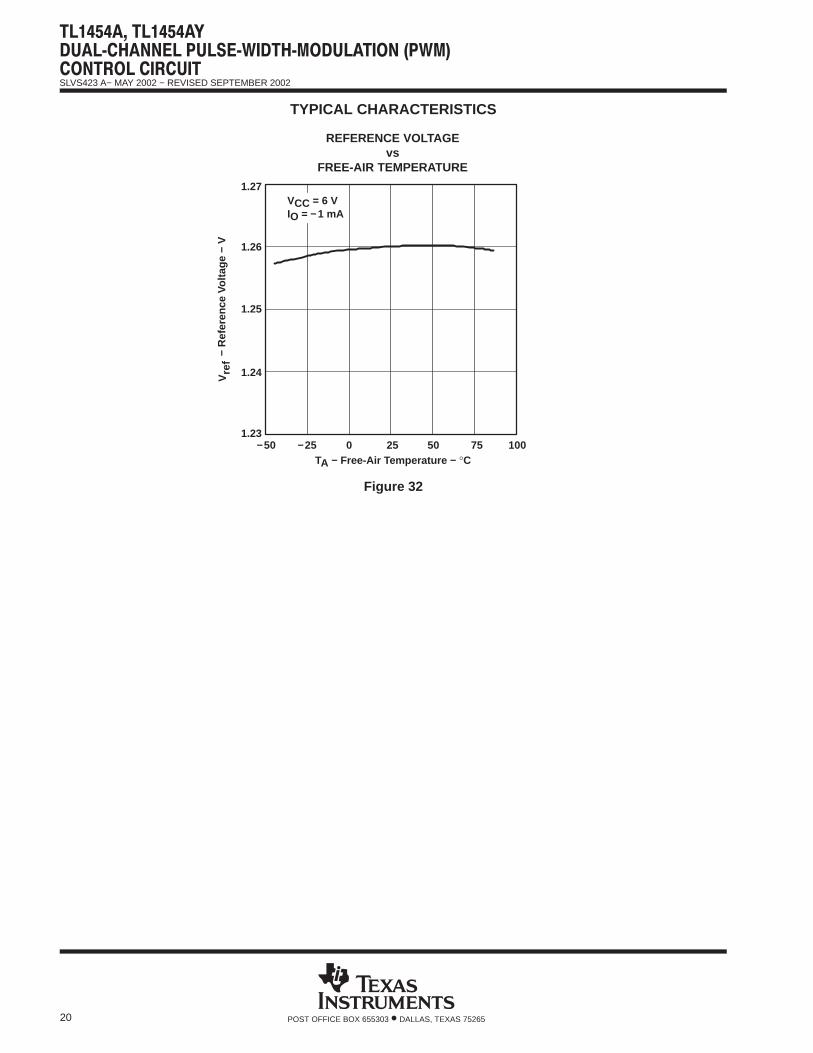
Figure 32

PACKAGE OPTION ADDENDUM
www.ti.com 13-Jul-2022
PACKAGING INFORMATION
Orderable Device Status(1)
Package Type PackageDrawing
Pins PackageQty
Eco Plan(2)
Lead finish/Ball material
(6)
MSL Peak Temp(3)
Op Temp (°C) Device Marking(4/5)
Samples
TL1454ACD ACTIVE SOIC D 16 40 RoHS & Green NIPDAU Level-1-260C-UNLIM -20 to 85 TL1454AC Samples
TL1454ACDBR ACTIVE SSOP DB 16 2000 RoHS & Green NIPDAU Level-1-260C-UNLIM -20 to 85 T1454A Samples
TL1454ACDG4 ACTIVE SOIC D 16 40 TBD Call TI Call TI -20 to 85 Samples
TL1454ACN ACTIVE PDIP N 16 25 RoHS & Green NIPDAU N / A for Pkg Type -20 to 85 TL1454ACN Samples
TL1454ACNSR ACTIVE SO NS 16 2000 RoHS & Green NIPDAU Level-1-260C-UNLIM -20 to 85 TL1454A Samples
TL1454ACPW ACTIVE TSSOP PW 16 90 RoHS & Green NIPDAU Level-1-260C-UNLIM -20 to 85 T1454A Samples
TL1454ACPWR ACTIVE TSSOP PW 16 2000 RoHS & Green NIPDAU Level-1-260C-UNLIM -20 to 85 T1454A Samples
(1) The marketing status values are defined as follows:ACTIVE: Product device recommended for new designs.LIFEBUY: TI has announced that the device will be discontinued, and a lifetime-buy period is in effect.NRND: Not recommended for new designs. Device is in production to support existing customers, but TI does not recommend using this part in a new design.PREVIEW: Device has been announced but is not in production. Samples may or may not be available.OBSOLETE: TI has discontinued the production of the device.
(2) RoHS: TI defines "RoHS" to mean semiconductor products that are compliant with the current EU RoHS requirements for all 10 RoHS substances, including the requirement that RoHS substancedo not exceed 0.1% by weight in homogeneous materials. Where designed to be soldered at high temperatures, "RoHS" products are suitable for use in specified lead-free processes. TI mayreference these types of products as "Pb-Free".RoHS Exempt: TI defines "RoHS Exempt" to mean products that contain lead but are compliant with EU RoHS pursuant to a specific EU RoHS exemption.Green: TI defines "Green" to mean the content of Chlorine (Cl) and Bromine (Br) based flame retardants meet JS709B low halogen requirements of <=1000ppm threshold. Antimony trioxide basedflame retardants must also meet the <=1000ppm threshold requirement.
(3) MSL, Peak Temp. - The Moisture Sensitivity Level rating according to the JEDEC industry standard classifications, and peak solder temperature.
(4) There may be additional marking, which relates to the logo, the lot trace code information, or the environmental category on the device.
(5) Multiple Device Markings will be inside parentheses. Only one Device Marking contained in parentheses and separated by a "~" will appear on a device. If a line is indented then it is a continuationof the previous line and the two combined represent the entire Device Marking for that device.
Addendum-Page 1

PACKAGE OPTION ADDENDUM
www.ti.com 13-Jul-2022
(6) Lead finish/Ball material - Orderable Devices may have multiple material finish options. Finish options are separated by a vertical ruled line. Lead finish/Ball material values may wrap to twolines if the finish value exceeds the maximum column width.
Important Information and Disclaimer:The information provided on this page represents TI's knowledge and belief as of the date that it is provided. TI bases its knowledge and belief on informationprovided by third parties, and makes no representation or warranty as to the accuracy of such information. Efforts are underway to better integrate information from third parties. TI has taken andcontinues to take reasonable steps to provide representative and accurate information but may not have conducted destructive testing or chemical analysis on incoming materials and chemicals.TI and TI suppliers consider certain information to be proprietary, and thus CAS numbers and other limited information may not be available for release.
In no event shall TI's liability arising out of such information exceed the total purchase price of the TI part(s) at issue in this document sold by TI to Customer on an annual basis.
Addendum-Page 2
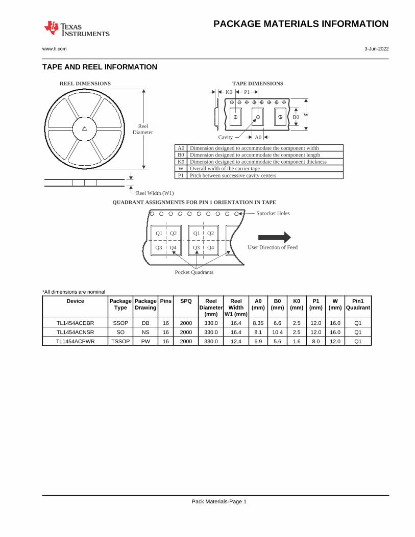
PACKAGE MATERIALS INFORMATION
www.ti.com 3-Jun-2022
TAPE AND REEL INFORMATION
Reel Width (W1)
REEL DIMENSIONS
A0B0K0W
Dimension designed to accommodate the component lengthDimension designed to accommodate the component thicknessOverall width of the carrier tapePitch between successive cavity centers
Dimension designed to accommodate the component width
TAPE DIMENSIONS
K0 P1
B0 W
A0Cavity
QUADRANT ASSIGNMENTS FOR PIN 1 ORIENTATION IN TAPE
Pocket Quadrants
Sprocket Holes
Q1 Q1Q2 Q2
Q3 Q3Q4 Q4 User Direction of Feed
P1
ReelDiameter
*All dimensions are nominal
Device PackageType
PackageDrawing
Pins SPQ ReelDiameter
(mm)
ReelWidth
W1 (mm)
A0(mm)
B0(mm)
K0(mm)
P1(mm)
W(mm)
Pin1Quadrant
TL1454ACDBR SSOP DB 16 2000 330.0 16.4 8.35 6.6 2.5 12.0 16.0 Q1
TL1454ACNSR SO NS 16 2000 330.0 16.4 8.1 10.4 2.5 12.0 16.0 Q1
TL1454ACPWR TSSOP PW 16 2000 330.0 12.4 6.9 5.6 1.6 8.0 12.0 Q1
Pack Materials-Page 1
PACKAGE MATERIALS INFORMATION
www.ti.com 3-Jun-2022
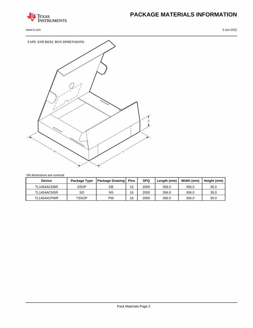
TAPE AND REEL BOX DIMENSIONS
Width (mm)
W L
H
*All dimensions are nominal
Device Package Type Package Drawing Pins SPQ Length (mm) Width (mm) Height (mm)
TL1454ACDBR SSOP DB 16 2000 356.0 356.0 35.0
TL1454ACNSR SO NS 16 2000 356.0 356.0 35.0
TL1454ACPWR TSSOP PW 16 2000 356.0 356.0 35.0
Pack Materials-Page 2
PACKAGE MATERIALS INFORMATION
www.ti.com 3-Jun-2022
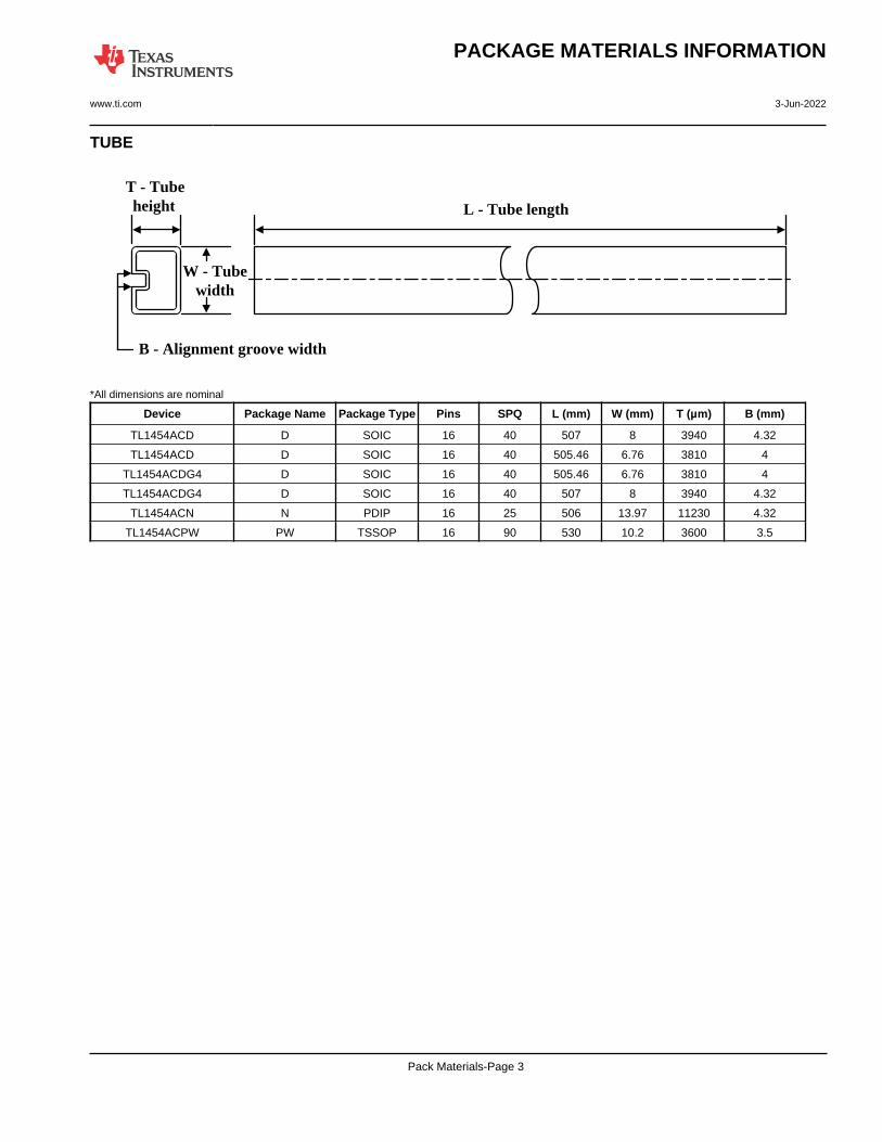
TUBE
L - Tube lengthT - Tube height
W - Tube width
B - Alignment groove width *All dimensions are nominal
Device Package Name Package Type Pins SPQ L (mm) W (mm) T (µm) B (mm)
TL1454ACD D SOIC 16 40 507 8 3940 4.32
TL1454ACD D SOIC 16 40 505.46 6.76 3810 4
TL1454ACDG4 D SOIC 16 40 505.46 6.76 3810 4
TL1454ACDG4 D SOIC 16 40 507 8 3940 4.32
TL1454ACN N PDIP 16 25 506 13.97 11230 4.32
TL1454ACPW PW TSSOP 16 90 530 10.2 3600 3.5
Pack Materials-Page 3

IMPORTANT NOTICE AND DISCLAIMERTI PROVIDES TECHNICAL AND RELIABILITY DATA (INCLUDING DATA SHEETS), DESIGN RESOURCES (INCLUDING REFERENCE DESIGNS), APPLICATION OR OTHER DESIGN ADVICE, WEB TOOLS, SAFETY INFORMATION, AND OTHER RESOURCES “AS IS” AND WITH ALL FAULTS, AND DISCLAIMS ALL WARRANTIES, EXPRESS AND IMPLIED, INCLUDING WITHOUT LIMITATION ANY IMPLIED WARRANTIES OF MERCHANTABILITY, FITNESS FOR A PARTICULAR PURPOSE OR NON-INFRINGEMENT OF THIRD PARTY INTELLECTUAL PROPERTY RIGHTS.These resources are intended for skilled developers designing with TI products. You are solely responsible for (1) selecting the appropriate TI products for your application, (2) designing, validating and testing your application, and (3) ensuring your application meets applicable standards, and any other safety, security, regulatory or other requirements.These resources are subject to change without notice. TI grants you permission to use these resources only for development of an application that uses the TI products described in the resource. Other reproduction and display of these resources is prohibited. No license is granted to any other TI intellectual property right or to any third party intellectual property right. TI disclaims responsibility for, and you will fully indemnify TI and its representatives against, any claims, damages, costs, losses, and liabilities arising out of your use of these resources.TI’s products are provided subject to TI’s Terms of Sale or other applicable terms available either on ti.com or provided in conjunction with such TI products. TI’s provision of these resources does not expand or otherwise alter TI’s applicable warranties or warranty disclaimers for TI products.TI objects to and rejects any additional or different terms you may have proposed. IMPORTANT NOTICE
Mailing Address: Texas Instruments, Post Office Box 655303, Dallas, Texas 75265Copyright © 2022, Texas Instruments Incorporated