
Circuit Properties of Zero-Voltage-Transition PWM Converters
16
Circuit Properties of Zero-Voltage-Transition PWM Converters 35 JPE 8-1-4 Circuit Properties of Zero-Voltage-Transition PWM Converters Amir Ostadi * , Xing Gao * and Gerry Moschopoulos † †* Dept. of Electrical and Electronics Eng., University of Western Ontario, London, Ontario, Canada ABSTRACT A zero-voltage-transition (ZVT) pulse width modulated (PWM) converter is a PWM converter with a single main power switch that has an auxiliary circuit to help it turn on with zero-voltage switching (ZVS). There have been many ZVT-PWM converters proposed in the literature as they are the most popular type of ZVS-PWM converters. In this paper, the properties and characteristics of several types of ZVT-PWM converters are reviewed. A new type of ZVT-PWM converter is then introduced, and the operation of a sample converter of this type is explained and analyzed in detail. A procedure for the design of the converter is presented and demonstrated experimentally. The feasibility of the new converter is confirmed with results obtained from an experimental prototype. Conclusions on the performance of ZVT-PWM converters in general are made based on the efficiency results obtained from the experimental prototypes of various ZVT-PWM converters of different types. Keywords: Zero-voltage transition, PWM converters, Switch-mode power supplies, High-frequency converters 1. Introduction High switching frequencies are used in power converters to reduce the size and weight of their magnetic and filter components, thus reducing overall converter size and weight. Operating at higher switching frequencies, however, increases switching losses, which reduces converter efficiency. Converters operating with high switching frequencies are, therefore, typically implemented with zero-voltage switching (ZVS) to minimize these problems. With ZVS, converter switches are made to operate with a zero-voltage turn-on and turn-off. In recent years, the most widely used single-switch pulse-width modulated (PWM) ZVS power converters have been so called zero-voltage-transition (ZVT) PWM converters. There have been many previously proposed ZVT-PWM converters (i.e. [1]-[14] ) and they all share certain common properties. These converters have an auxiliary circuit connected in parallel to the main switch to help it turn on with ZVS and a snubber capacitor to help the switch turn off with ZVS, as shown in Fig. 1. They operate in the same manner as regular PWM converters, but with reduced switching losses. This reduction is due to the fact that the auxiliary circuit operates for only a small portion of the switching cycle and is activated just before the main converter switch is about to be turned on. Since the auxiliary circuit is on for such a short time, a device with better switching characteristics than that used as the main switch can be chosen, as conduction losses are not an issue. Manuscript received Oct. 1, 2007; revised Nov. 19, 2007 † Corresponding Author: [email protected] Tel: 519-661-2111, Fax: 519-850-2436, Univ. of Western Ontario * Dept. of Elec. and Comp. Eng. Univ. of Western Ontario
-
Upload
khangminh22 -
Category
Documents
-
view
4 -
download
0
Transcript of Circuit Properties of Zero-Voltage-Transition PWM Converters
Circuit Properties of Zero-Voltage-Transition PWM Converters 35
JPE 8-1-4
Circuit Properties of Zero-Voltage-Transition PWM Converters
Amir Ostadi*, Xing Gao* and Gerry Moschopoulos†
†*Dept. of Electrical and Electronics Eng., University of Western Ontario, London, Ontario, Canada
ABSTRACT
A zero-voltage-transition (ZVT) pulse width modulated (PWM) converter is a PWM converter with a single main power switch that has an auxiliary circuit to help it turn on with zero-voltage switching (ZVS). There have been many ZVT-PWM converters proposed in the literature as they are the most popular type of ZVS-PWM converters. In this paper, the properties and characteristics of several types of ZVT-PWM converters are reviewed. A new type of ZVT-PWM converter is then introduced, and the operation of a sample converter of this type is explained and analyzed in detail. A procedure for the design of the converter is presented and demonstrated experimentally. The feasibility of the new converter is confirmed with results obtained from an experimental prototype. Conclusions on the performance of ZVT-PWM converters in general are made based on the efficiency results obtained from the experimental prototypes of various ZVT-PWM converters of different types.
Keywords: Zero-voltage transition, PWM converters, Switch-mode power supplies, High-frequency converters
1. Introduction
High switching frequencies are used in power converters to reduce the size and weight of their magnetic and filter components, thus reducing overall converter size and weight. Operating at higher switching frequencies, however, increases switching losses, which reduces converter efficiency. Converters operating with high switching frequencies are, therefore, typically implemented with zero-voltage switching (ZVS) to minimize these problems. With ZVS, converter switches are made to operate with a zero-voltage turn-on and turn-off.
In recent years, the most widely used single-switch
pulse-width modulated (PWM) ZVS power converters have been so called zero-voltage-transition (ZVT) PWM converters. There have been many previously proposed ZVT-PWM converters (i.e. [1]-[14]) and they all share certain common properties. These converters have an auxiliary circuit connected in parallel to the main switch to help it turn on with ZVS and a snubber capacitor to help the switch turn off with ZVS, as shown in Fig. 1. They operate in the same manner as regular PWM converters, but with reduced switching losses. This reduction is due to the fact that the auxiliary circuit operates for only a small portion of the switching cycle and is activated just before the main converter switch is about to be turned on. Since the auxiliary circuit is on for such a short time, a device with better switching characteristics than that used as the main switch can be chosen, as conduction losses are not an issue.
Manuscript received Oct. 1, 2007; revised Nov. 19, 2007 †Corresponding Author: [email protected]
Tel: 519-661-2111, Fax: 519-850-2436, Univ. of Western Ontario *Dept. of Elec. and Comp. Eng. Univ. of Western Ontario
36 Journal of Power Electronics, Vol. 8, No. 1, January 2008
The objectives of this paper are as follows: (i) To review the basic circuit properties of ZVT-PWM
converters for design engineers who may not be familiar with them;
(ii) To determine if it is possible to maximize the efficiency of these converters using these circuit properties.
In this paper, the properties and characteristics of several types of ZVT-PWM converters are reviewed. A new type of ZVT-PWM converter is then introduced and the operation of an experimental converter of this type is then demonstrated. The feasibility of the new converter is confirmed with results obtained from an experimental prototype. Conclusions on the performance of the converter and on the performance of ZVT-PWM converters in general are made based on efficiency results obtained from experimental prototypes of other ZVT-PWM converters that are representative of different types.
2. Non-Resonant and Resonant Auxiliary Circuits in ZVT-PWM Converters
There have been many auxiliary circuits that have been
previously proposed for use in ZVT-PWM converters [14]. With few exceptions, auxiliary circuits in ZVT-PWM converters are generally one of three types: non-resonant circuits, resonant circuits that have an LC resonant network placed in series with the auxiliary circuit switch, or dual circuits that are a combination of the first two types. The operation of a ZVT-PWM boost converter with an experimental non-resonant and an experimental resonant auxiliary circuit is reviewed in this section of the paper.
The operation of a ZVT-PWM boost converter with an experimental dual circuit will be reviewed in the next section.
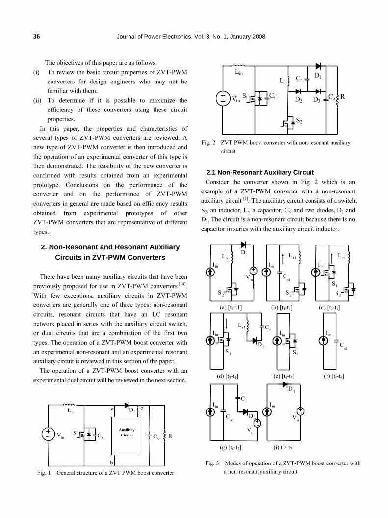
2.1 Non-Resonant Auxiliary Circuit Consider the converter shown in Fig. 2 which is an
example of a ZVT-PWM converter with a non-resonant auxiliary circuit [1]. The auxiliary circuit consists of a switch, S2, an inductor, Lr, a capacitor, Cr, and two diodes, D2 and D3. The circuit is a non-resonant circuit because there is no capacitor in series with the auxiliary circuit inductor.
V in C s1 C o R
L in
S 1
D 1
Auxiliary Circuit
a
b
c
Fig. 1 General structure of a ZVT PWM boost converter
VinCs1
Lr
Co R
Lin
S1
S2
D1
D2
Cr
D3
Fig. 2 ZVT-PWM boost converter with non-resonant auxiliary
circuit
I in
V o
D 1L r1
S 2
I in
C s1
S 2
L r1
I in
S 2
L r1
S 1
(a) [t0-t1] (b) [t1-t2] (c) [t2-t3]
I in
D 2
Lr1
S 1
CrI in
S 1
I in
Cs1
(d) [t3-t4] (e) [t4-t5] (f) [t5-t6]
Vo
D 3
CrIin
Cs1
I in V o
D 1
(g) [t6-t7] (i) t > t7
Fig. 3 Modes of operation of a ZVT-PWM boost converter with
a non-resonant auxiliary circuit

Circuit Properties of Zero-Voltage-Transition PWM Converters 37
Fig. 3 shows circuit diagrams of the modes of operation
that the converter shown in Fig. 2 goes through during a switching cycle. For these diagrams, the input inductor, Lin, is assumed large enough to be considered as a constant current source, Iin, and the output capacitor, Co, is large enough to be considered as a voltage source, Vo.. Typical waveforms that illustrate the converter's operation are shown in Fig. 4.
The converter works as follows: Before the auxiliary switch S2 is turned on to help the main switch S1 turn on with ZVS, current flows through the main power boost diode D1. At some time t = t0, the auxiliary switch S2 is turned on and current begins to be diverted from D1 to the auxiliary circuit. Since there is an inductor in series with the switch, it is turned on with zero-current switching (ZCS) as the inductor slows down the rate of current rise
in the switch. At t = t1, there is no current flowing in D1 and capacitor Cs1 begins to discharge as the voltage across it is now not clamped to the output voltage. Cs1 is totally discharged at some time t = t2 and the body diode of S1 conducts current. S1 can be turned on with ZVS as the voltage across Cs1 is almost zero.
Once S1 has been turned on, S2 can be turned off at some time t = t3. When this happens, the current through Lr is diverted to D2 and charges capacitor Cr and the current in S1 stops flowing through the body diode and instead flows through the switch. When the current through Lr becomes zero at some time t = t4, the converter then operates like a conventional PFC boost converter. S1 is turned off at t = t5 and capacitor Cs1 is charged until D3 begins to conduct at t = t6. Cr is eventually discharged through D3 and current then flows through D1 at t = t7 until S1 is turned on again to start a new switching cycle.
The following facts, which are true for all ZVT-PWM converters with non-resonant auxiliary circuits, should be noted: (i) The current flowing through the auxiliary switch is
interrupted when the switch is turned off. Although the switch has a hard turn-off that somewhat offsets the gain in efficiency that is derived by having the auxiliary circuit in the circuit, these turn-off losses are still less than the turn-on losses of the main power switch in a conventional PWM converter.
(ii) The operation of the auxiliary circuit in the converter does not affect the voltage or current stress of the main power switch or the main power boost diode.
Other non-resonant auxiliary circuits that can be used in ZVT-PWM converters were proposed in [2], [4], [8], [9]; some of these are shown in Fig. 5. Regardless of how these circuits may look, the fundamental circuit properties of all non-resonant circuits are the same. The only real difference is in the way that energy is transferred out of the auxiliary circuit after the auxiliary switch is turned off.
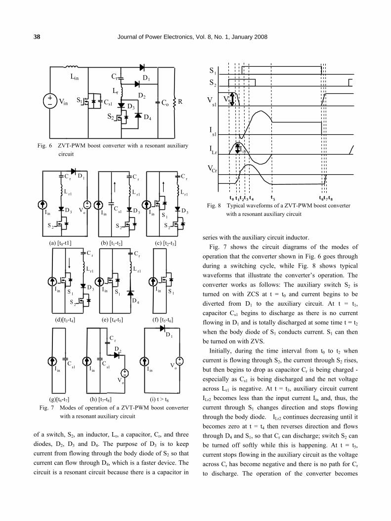
2.2 ZVT-PWM Converter with Resonant Auxiliary Circuit
Consider the converter shown in Fig. 6, which is an example of a ZVT-PWM converter with a resonant auxiliary circuit [5], [6]. The auxiliary circuit consists
S 1
S 2
V s1
I s1
I Lr I in
V Cr
t 5 t 7 t 6
V o
t 0 t 1 t 2 t 3 t 4 Fig. 4 Typical waveforms of a ZVT-PWM boost converter
with a non-resonant auxiliary circuit
b
c
a
b
c
a
Fig. 5 Other non-resonant auxiliary circuits
38 Journal of Power Electronics, Vol. 8, No. 1, January 2008
of a switch, S2, an inductor, Lr, a capacitor, Cr, and three diodes, D2, D3 and D4. The purpose of D3 is to keep current from flowing through the body diode of S2 so that current can flow through D4, which is a faster device. The circuit is a resonant circuit because there is a capacitor in
series with the auxiliary circuit inductor. Fig. 7 shows the circuit diagrams of the modes of
operation that the converter shown in Fig. 6 goes through during a switching cycle, while Fig. 8 shows typical waveforms that illustrate the converter’s operation. The converter works as follows: The auxiliary switch S2 is turned on with ZCS at t = t0 and current begins to be diverted from D1 to the auxiliary circuit. At t = t1, capacitor Cs1 begins to discharge as there is no current flowing in D1 and is totally discharged at some time t = t2 when the body diode of S1 conducts current. S1 can then be turned on with ZVS.
Initially, during the time interval from t0 to t2 when current is flowing through S2, the current through S2 rises, but then begins to drop as capacitor Cr is being charged - especially as Cs1 is being discharged and the net voltage across Lr1 is negative. At t = t3, auxiliary circuit current ILr2 becomes less than the input current Iin and, thus, the current through S1 changes direction and stops flowing through the body diode. ILr2 continues decreasing until it becomes zero at t = t4 then reverses direction and flows through D4 and S1, so that Cr can discharge; switch S2 can be turned off softly while this is happening. At t = t5, current stops flowing in the auxiliary circuit as the voltage across Cr has become negative and there is no path for Cr to discharge. The operation of the converter becomes
Vin Cs1 Co R
Lin
S1
D1 Cr
Lr D2
S2 D4 D3
Fig. 6 ZVT-PWM boost converter with a resonant auxiliary
circuit
D 1
D 3
L r1
S 2
C r
I in V o
Cs1 D 3
L r1
S 2
C r
I in
S 1D 3
Lr1
S 2
C r
I in
(a) [t0-t1] (b) [t1-t2] (c) [t2-t3]
S 1 D 3
L r1
S 2
C r
I in
D 4 S1
L r1
C r
I in
I in S 1
(d)[t3-t4] (e) [t4-t5] (f) [t5-t6]
I in C
s1
V o
D 2 C r
I in C
s1
Vo
D 1
I in
(g)[t6-t7] (h) [t7-t8] (i) t > t8 Fig. 7 Modes of operation of a ZVT-PWM boost converter
with a resonant auxiliary circuit
S1
S2
Vs1
Is1
ILr Iin
Vo
VCr
t0 t1t2t3 t 6t4 t8t7t5
Fig. 8 Typical waveforms of a ZVT-PWM boost converter with a resonant auxiliary circuit
Circuit Properties of Zero-Voltage-Transition PWM Converters 39
identical to that of the converter shown in Fig. 2 until the start of the next switching cycle.
The following facts, which are true for all ZVT-PWM converters with resonant auxiliary circuits, should be noted: (i) The series inductor-capacitor components in the
auxiliary circuit force the auxiliary switch current to drop to zero naturally so that there is no current flowing through the auxiliary switch when the switch is turned off. The switch is turned off softly while current is flowing through diode D4, which is anti-parallel to it.
(ii) The operation of the auxiliary circuit in the converter results in an increase in the peak current stress of the main power switch S1 due to the auxiliary circuit current that flows through D4 when it is in its negative resonant half-cycle. This circulating current increases both the peak current stress of the main switch and conduction losses.
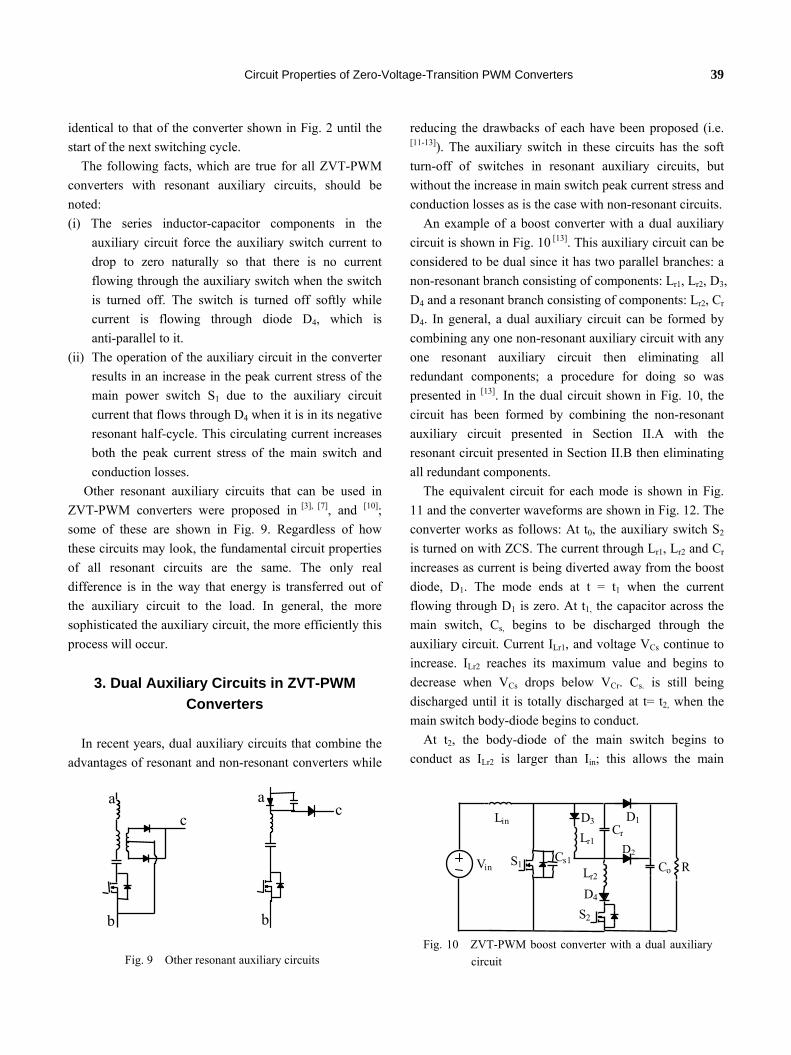
Other resonant auxiliary circuits that can be used in ZVT-PWM converters were proposed in [3], [7], and [10]; some of these are shown in Fig. 9. Regardless of how these circuits may look, the fundamental circuit properties of all resonant circuits are the same. The only real difference is in the way that energy is transferred out of the auxiliary circuit to the load. In general, the more sophisticated the auxiliary circuit, the more efficiently this process will occur.
3. Dual Auxiliary Circuits in ZVT-PWM Converters
In recent years, dual auxiliary circuits that combine the
advantages of resonant and non-resonant converters while
reducing the drawbacks of each have been proposed (i.e. [11-13]). The auxiliary switch in these circuits has the soft turn-off of switches in resonant auxiliary circuits, but without the increase in main switch peak current stress and conduction losses as is the case with non-resonant circuits.
An example of a boost converter with a dual auxiliary circuit is shown in Fig. 10 [13]. This auxiliary circuit can be considered to be dual since it has two parallel branches: a non-resonant branch consisting of components: Lr1, Lr2, D3, D4 and a resonant branch consisting of components: Lr2, Cr D4. In general, a dual auxiliary circuit can be formed by combining any one non-resonant auxiliary circuit with any one resonant auxiliary circuit then eliminating all redundant components; a procedure for doing so was presented in [13]. In the dual circuit shown in Fig. 10, the circuit has been formed by combining the non-resonant auxiliary circuit presented in Section II.A with the resonant circuit presented in Section II.B then eliminating all redundant components.
The equivalent circuit for each mode is shown in Fig. 11 and the converter waveforms are shown in Fig. 12. The converter works as follows: At t0, the auxiliary switch S2 is turned on with ZCS. The current through Lr1, Lr2 and Cr increases as current is being diverted away from the boost diode, D1. The mode ends at t = t1 when the current flowing through D1 is zero. At t1, the capacitor across the main switch, Cs, begins to be discharged through the auxiliary circuit. Current ILr1, and voltage VCs continue to increase. ILr2 reaches its maximum value and begins to decrease when VCs drops below VCr. Cs. is still being discharged until it is totally discharged at t= t2, when the main switch body-diode begins to conduct.
At t2, the body-diode of the main switch begins to conduct as ILr2 is larger than Iin; this allows the main
b
c a
b
ca
Fig. 9 Other resonant auxiliary circuits
VinCs1 Co R
Lin
S1
D1 Cr
D3
Lr2
D2
D4
Lr1
S2
Fig. 10 ZVT-PWM boost converter with a dual auxiliary circuit

40 Journal of Power Electronics, Vol. 8, No. 1, January 2008
switch S1 to be turned on with ZVS. Current ILr1 and voltage VCr continue to increase. Some time during this mode, a resonant process involving the resonant branch of the auxiliary circuit begins and currents ICr and ILr2 start to decrease. It continues to do so until t = t3, when the main switch S1 can be turned on with ZVS. At t3, current stops flowing through the body-diode of main switch S1 and starts flowing through the switch. The resonant process that began earlier continues as current ILr1 and voltage VCr continue to increase and currents ICr and ILr2 continue to decrease.
At t = t4, ILr2 becomes zero and ILr1 = ICr as diode D4
blocks any negative resonant current that would otherwise flow. The auxiliary switch can be turned off with ZCS as there is no current flowing through it. The current through the main switch is equal to iin and the energy from
inductor Lr1 is transferred to Cr until t=t5 when the current through Lr1 becomes zero and diode D3 prevents the current from reversing direction. The operation of the converter from time t5 onwards (Fig. 11(f)-(i)), when current no longer flows in the auxiliary circuit, is exactly the same as that of the ZVT-PWM converter with the non-resonant auxiliary circuit discussed in Section II.A (Fig. 3(f)-(i)).
It can be seen from Fig. 11(e) that the switch in the dual auxiliary circuit, like the switch in any dual auxiliary circuit, is turned off softly while current is diverted away from the switch by the resonant branch, but without any circulating current fed back into the main power switch as it is contained in the auxiliary circuit.
4. An Off-Tuned Dual Auxiliary Circuit Presently, dual auxiliary circuits are the most efficient
V o
D 1 D 3
D 4
L r1
S 2
C r
L r2 I in
I in
D 3
D 4
L r1
S 2
C r
L r2I in
C s1
I in
D 3
D 4
L r1
S 1 S 2
C r
Lr2
(a) [t0-t1] (b) [t1-t2] (c) [t2-t3]
I in
D 3
D 4
L r1
S 1 S 2
C r
L r2
I in
D 3 L r1
S 1
C r
I in S 1
(d) [t3-t4] (e) [t4-t5] (f) [t5-t6]
I in C
s1
Vo
D 2
C r
I in C
s1
Vo
D 1
I in
(g) [t6-t7] (h) [t7-t8] (i) t > t8 Fig. 11 Modes of operation of a ZVT-PWM boost converter
with a dual auxiliary circuit
S 1
S2
Vs1I s1
ILr2
Vs2Is2
Iin
VCr
ILr1
t0 t1t2t3 t6 t8t4 t7t 5 t9
Vo
Iin Vo
Fig. 12 Typical waveforms of a ZVT-PWM boost converter
with a dual auxiliary circuit
Is2
ta tb td t e t c tf
I in
t
Non-Resonant Resonant
Fig. 13 Auxiliary switch current waveforms of a ZVT-PWM
boost converter

Circuit Properties of Zero-Voltage-Transition PWM Converters 41
type of auxiliary circuits in ZVT-PWM converters because they have lower switching losses than non-resonant auxiliary circuits and lower conduction losses than resonant auxiliary circuits. One question that can be asked, however, is whether it is possible to further improve the efficiency of dual auxiliary circuits - what would it take to maximize the efficiency of auxiliary circuits in ZVT-PWM converters?
To answer this question, consider the auxiliary switch current waveforms shown in Fig. 13. If the auxiliary switch S2 is turned on at some time ta to discharge the capacitance across the main power switch S1, then it is turned off at time tc. If the switch is in a non-resonant auxiliary circuit, tc is when the auxiliary switch current Is2 is greater than the input current Iin after tb; if it is a dual auxiliary circuit, tc is at time te ; if it is in a resonant auxiliary circuit, tc is some time between te and tf . In the case of a resonant auxiliary circuit, current would continue to flow through the anti-parallel diode across the switch until tf.
Let us say that the auxiliary switch is turned off at time tc in Fig. 13. If this is done, it can be seen that the switch will be turned off with some current flowing through it, but this current will still be significantly less than it would be if the switch were turned off at tc than it would be if it were in a non-resonant circuit. Moreover, any increase in conduction losses would be fairly small. Turning the switch off at tc would also result in the switch conducting even less current than it would if it were in a dual auxiliary circuit and significantly less current that it would if it were in a resonant auxiliary circuit. Interrupting the resonant cycle of the auxiliary switch current would reduce the current circulating in the auxiliary circuit.
Although the turn-off losses in the auxiliary switch are greater than those of a switch in a dual or resonant
auxiliary circuit, these losses are more than offset by the reduction in conduction losses.
In terms of circuit implementation, an auxiliary circuit can be made to operate in this way if the resonant branch of the dual circuit is "off-tuned" so that the current through the auxiliary switch is reduced, but not completely eliminated, before it is turned off. This is in contrast to the "appropriate" tuning of the resonant branch in a dual auxiliary circuit so that the auxiliary switch turns off with zero current. Fig. 14 shows an example a ZVT-PWM boost converter with an off-tuned variation of the dual auxiliary circuit in Fig. 10.
Just like a dual auxiliary circuit, the circuit in Fig. 14 has a non-resonant branch and a resonant branch. The non-resonant branch consists of components Lr1, D3 and D4, and the resonant branch consists of components Lr2, Cr, D4. Components D2 and Cr* are added to provide a path where the remaining auxiliary switch current can be diverted when the switch is turned off. This is needed as the switch does not turn off softly. Energy from Lr1 and Lr2 is transferred to Cr*. Diodes D6 and D5 allow the voltages across capacitors Cr and Cr*, respectively, to return to zero every cycle by transferring the energy in these capacitors to the output each cycle.
Fig. 15 shows the circuit diagrams of the modes of operation that the converter shown in Fig. 14 goes through during a switching cycle. The converter's modes of operation are as follows:
Mode 1 (t0-t1): At t0, the auxiliary switch S2 is turned on and current begins to be diverted away from the boost diode, D1. S2 turns on with ZCS due to the presence of inductors in both circuit branches. The equations that define this mode are given in equs. (1) to (3):
orcr Vdtdi
Lv =+ 22 (1) or V
dtdi
L =11 (2)
dtdv
Ci crr=2 (3)
The solutions to the above equations are given below by
equs. (4) to (7).The resonant frequency in this mode is given by (8).
( )( )tVv ocr 0cos1 ω−= (4) oc Vtvs
=)( (5)
V in C s1 Co R
L in
S 1
D 1 D 3
D 2
D 4
L r1
S 2
D 5
D 6 C r
C r * Lr2
Fig. 14 A ZVT-PWM boost converter with an off-tuned dual
auxiliary circuit

42 Journal of Power Electronics, Vol. 8, No. 1, January 2008
tLV
ir
o
1
1 = (6)
( )tVCi or 002 sin ωω= (7)
where
rr CL2
10 =ω (8)
Mode 2 (t1-t2): At t = t1, the current flowing through D1
is zero and the capacitor of the main switch Cs1 begins to be discharged through the auxiliary circuit. The current through Lr1 continues to rise during this interval. The current through Lr2 rises until the voltages across capacitors Cs1 and Cr become equal, and then starts decreasing. The equations that define this mode are given in equs. (9) to (12):
dtdi
Lv rcs
11= (9)
dtdi
Lvv rcc rs
22+= (10)
dt
dvCi rc
r=2 (11)
dt
dvCIii sc
sin −=+ 21 (12)
Equation (13) defines the voltage across the capacitor
Cr. The other parameters (i1, i2 and scv ) are defined based
on equs. (14) to (16):
( ) ( ) ( ) ( )tBtAtBtAv ddddcr 2211sincossincos 2211 ωωωω +++= (13)
dt
dvCi rc
r=2 (14)
2
2
2dt
vdCLvv r
rs
crrcc += (15)
( )3
3
21dt
vdCCL
dt
dvCCi rr c
srrc
sr −+−= (16)
where
24 4
241
21
1
ωωωω
−+=d (17)
24 4
241
21
2
ωωωω
−−=d (18)
and A1 ,A2 ,B1 ,B2 ,D1,D2, ω1, and ω2 are given below
⎟⎟⎠
⎞⎜⎜⎝
⎛ ++=
rCCLLsCLrCLL
srr
rrr
21
12121
)(ω (19)
⎟⎟⎠
⎞⎜⎜⎝
⎛=
rsrr CCLL 21
42
1ω (20)
( ) ( )( ) ⎟⎟
⎟
⎠
⎞
⎜⎜⎜
⎝
⎛
−
+−=
rrdd
orcrrd
CL
VtVCLA
222
122
112
21
ωω
ω (21)
( ) ( )( ) ⎟⎟
⎟
⎠
⎞
⎜⎜⎜
⎝
⎛
−
+−=
rrdd
orcrrd
CL
VtVCLA
222
122
221
11
ωω
ω (22)
( )
( )⎟⎟⎟⎟⎟
⎠
⎞
⎜⎜⎜⎜⎜
⎝
⎛
−
⎟⎟⎠
⎞⎜⎜⎝
⎛−
=rddd
rrd
C
tICL
B112
2
22
122
2
1
1
ωωω
ω (23)
V o
D 1 D 3
D 4
L r1
S 2
C r L r2
I in
D 3
D 4
L r1
S 2
C r L r2
I in C
s1
I in
D 3
D 4
L r1
S 1
S 2
C r
L r2
(a) [t0-t1] (b) [t1-t2] (c) [t2-t3]
I in
D 3
D 4
L r1
S 1 S 2
C r L r2
I in
D 3
D 2 L r1
S 1
C r C r *
L r2
I in
D3
L r1
S 1
C r
L r2
(d) [t3-t4] (e) [t4-t5] (f) [t5-t6]
I in S 1
I in C
s1
V o
D 5
D 6 C r
C r *
I in C
s1
Vo
D 1
Iin
(g) [t6-t7] (h) [t7-t8] (i) [t8-t9] (j) t > t9
Fig. 15 Modes of operation of a ZVT-PWM boost converter
with an off-tuned dual auxiliary circuit
Circuit Properties of Zero-Voltage-Transition PWM Converters 43
( )
( )⎟⎟⎟⎟⎟
⎠
⎞
⎜⎜⎜⎜⎜
⎝
⎛
−
⎟⎟⎠
⎞⎜⎜⎝
⎛−
=rddd
rrd
C
tICL
B221
1
22
122
2
2
1
ωωω
ω (24)
Mode 3 (t2-t3): Cs1 is totally discharged at t = t2 and the
main switch body-diode begins to conduct as the combined current flowing through both auxiliary circuit branches is greater than the input current Iin. The current through Lr1, ILr1, is constant because the voltage across the inductor is zero during this mode. Voltage VCr continues to increase as current ILr2 passes through it and ILr2 continues decreasing because of the negative voltage across the inductor. While current is flowing through the body-diode of S1, this switch can be turned on with ZVS. The equations that define this mode are given in equs. (25) to (27):
022 =+
dtdi
Lv rcr (25)
011 =
dtdi
Lr (26)
dt
dvCi rc
r=2 (27)
The solutions to the above equations are given below by equs. (28) to (30). The resonant frequency in this mode is given by (31).
( ) ( ) ( ) ( )tC
tIttVv
rcc rr 0
2202 sin
0cos ω
ωω += (28) ( )211 tIi = (29)
( ) ( ) ( ) ( )ttVCttIircr 0200222 cossin ωωω −= (30)
rr CL 20
1=ω (31)
Mode 4 (t3-t4): At t = t3, the combined current flowing
through both branches of the auxiliary circuit reaches the input current Iin as the resonant process that began in Mode 3 continues. This results in current ceasing to flow through the body-diode of S1 and beginning to flow through the switch itself. Current ILr1 still remains constant
because the voltage across it is zero when current is passing through the main switch. Voltage VCr continues to increase during Mode 4 as current ILr2 continues to decrease. The voltage and current equations associated with this mode of operation are as follows where the resonant frequency was defined in the last mode of operation:
( ) ( ) ( ) ( )tC
tIttVv
rcc rr 0
0
3203 sincos ω
ωω += (32)
( )211 tIi = (33)
( ) ( ) ( ) ( )ttVCttIircr 0300322 cossin ωωω += (34)
Mode 5 (t4-t5): At t = t4, the auxiliary switch S2 is
turned off and the current in both auxiliary circuit branches flows through diode D2 to charge Cr*. The equations associated with this mode are
dtdi
Lv rcr
11* = (35)
dt
diLvv rcc rr
22* += (36)
dt
dvCi rc
r=2 (37)
0*
*21 =++
dt
dvCii rc
r (38)
Equ. (39) defines the voltage across Cr and the equations for the other parameters can be derived from this equation as follows:
( ) ( ) ( ) ( )tBtAtBtAv ddddcr 2211sincossincos 2211 ωωωω +++= (39)
dt
dvCi rc
r=2 (40)
2
2
2*dt
vdCLvv r
rr
crrcc
+= (41)
( )3
3*
2*
1dt
vdCCL
dt
dvCCi rr c
rrrc
rr −+−= (42)

44 Journal of Power Electronics, Vol. 8, No. 1, January 2008
where
24 4
241
21
1
ωωωω
−+=d (43)
24 4
241
21
2
ωωωω
−−=d
(44)
⎟⎟⎠
⎞⎜⎜⎝
⎛ ++=
rrrr
rrrrr
CCLL
CLCLL*
21
*1122
1)(
ω (45)
⎟⎟⎠
⎞⎜⎜⎝
⎛=
rrrr CCLL *21
42
1ω (46)
( ) ( )( ) ⎟
⎟
⎠
⎞
⎜⎜
⎝
⎛
−
−=
rrdd
crrd
CL
tVCLA r
222
422
112
21
ωω
ω (47)
( ) ( )( ) ⎟
⎟
⎠
⎞
⎜⎜
⎝
⎛
−
−=
rrdd
crrd
CL
tVCLA r
222
422
221
11
ωω
ω (48)
( )
( )
( ) ( )
( )⎟⎟⎟⎟⎟
⎠
⎞
⎜⎜⎜⎜⎜
⎝
⎛
−
+
−
⎟⎟⎟⎟⎟
⎠
⎞
⎜⎜⎜⎜⎜
⎝
⎛
−
⎟⎟⎠
⎞⎜⎜⎝
⎛−
=rddd
rr
rddd
rrd
CCL
tItI
C
tICL
B112112
22
*2
4221
22
422
22
1
1
ωωωωωω
ω (49)
( )
( )
( ) ( )
( )⎟⎟⎟⎟⎟
⎠
⎞
⎜⎜⎜⎜⎜
⎝
⎛
−
+
−
⎟⎟⎟⎟⎟
⎠
⎞
⎜⎜⎜⎜⎜
⎝
⎛
−
⎟⎟⎠
⎞⎜⎜⎝
⎛−
=rddd
rr
rddd
rrd
CCL
tItI
C
tICL
B221221
1
22
*2
4221
22
422
2
2
1
ωωωωωω
ω (50)
Mode 6 (t5-t6): At t=t5, current stops flowing through D2 and Cr*. This is usually because current in the resonant branch has reversed direction and has diverted the non-resonant branch current away from D2 so that the current flowing "up" the resonant branch is equal to the current flowing "down" the non-resonant branch. A resonant circuit between Lr1, Lr2 and Cr is created and current continues to flow in the auxiliary circuit until the current through Lr1 and Lr2 becomes zero. Diode D3 prevents the current from reversing direction and Capacitor Cr has a negative voltage at the end of this mode. The equations that define this mode are
dtdi
Lvdtdi
L rcr r
22
11 += (51)
dt
dvCii rc
r−=−= 21 (52)
and they can be solved to give
( ) ( ) ( ) ( )tC
tIttVv
rcc rr 0
0
5205 sincos ω
ωω += (53)
( ) ( ) ( ) ( )ttVCttIircr 0500522 sincos ωωω −= (54)
where
( ) rrr CLL 210
1+
=ω (55)
It should be noted that Mode 6 may be bypassed if
Mode 5 ends with the current in each auxiliary branch falling to zero by the end of the Mode, but this rarely happens. It may also be possible for the converter to temporarily slip into Mode 5 if the voltage across Cr is more "negative" than that across Cr*. If this happens, then the converter may slip back and forth between Modes 5 and 6 until current stops flowing in the auxiliary circuit.
Mode 7 (t6-t7): At t=t6, current is no longer flowing in the auxiliary circuit. The converter operates in the same way as a standard PWM boost converter during this mode.
Mode 8 (t7-t8): At t = t7, the main switch S1 turns off with ZVS as capacitor Cs1 slows down the rate of voltage increase as it begins to be charged by Iin.
Mode 9 (t8-t9): At t = t8, either the sum of VCs1 and VCr is equal to Vo, which causes D6 to conduct, or the sum of VCs1 and VCr* is equal to Vo, which causes D5 to conduct. Eventually, during this mode, both D5 and D6 conduct as both these capacitors are discharged by the input current while Cs1 is being charged.
Mode 10 (t>t9): At t=t9, Cr and Cr* are both fully discharged and Iin starts flowing through D1. The converter operates like a standard PWM converter until the auxiliary switch is turned on at the start of the next switching cycle.
5. Design of an Off-Tuned Auxiliary Circuit
Simple, experimental prototypes of a PWM boost
converter implemented with the non-resonant, resonant, dual and off-tuned auxiliary circuits discussed in this paper were built so that a comparative study of the
Circuit Properties of Zero-Voltage-Transition PWM Converters 45
performance of these converters could be made. In order to show how the off-tuned auxiliary circuit shown in Fig. 14 was designed, a design procedure is presented and demonstrated with a sample in this section of the paper. It is based on an analysis of the steady-state characteristics of the converter, which can be determined from the mode equations derived in Section IV, as shown in [7]. The procedure is iterative and the example shown represents the final iteration. The design of the components of the main power boost converter (i.e. the main boost switch) will not be discussed as it is the same as that of a standard PWM boost converter, nor will that of capacitor Cr* as it is basically a snubber capacitor that has little impact on the operation of the auxiliary circuit.
For the example, the auxiliary circuit is to be designed for a boost converter with the following parameters: Lin = 1 mH, S1 - IRFP460A MOSFET, and D1 - HFA25TB60 diode. The converter operates according to the following specifications: Input voltage Vin = 100 - 250V, output voltage Vo = 400V, maximum output power Po = 500 W, switching frequency fsw=100 kHz. The value of Cr* is 1.2 nF. The estimated efficiency for this final iteration is η=95%.
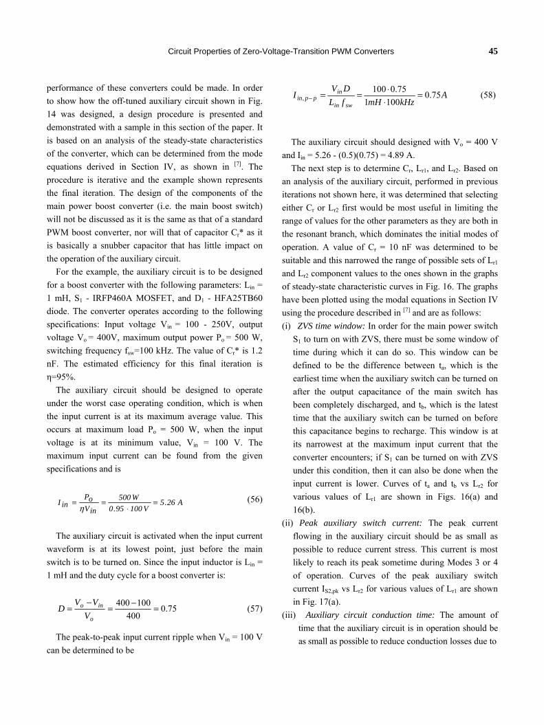
The auxiliary circuit should be designed to operate under the worst case operating condition, which is when the input current is at its maximum average value. This occurs at maximum load Po = 500 W, when the input voltage is at its minimum value, Vin = 100 V. The maximum input current can be found from the given specifications and is
A26.5V10095.0
W500
inVoP
inI =⋅
==η
(56)
The auxiliary circuit is activated when the input current waveform is at its lowest point, just before the main switch is to be turned on. Since the input inductor is Lin = 1 mH and the duty cycle for a boost converter is:
75.0400
100400 =−=−
=o
ino
VVV
D (57)
The peak-to-peak input current ripple when Vin = 100 V can be determined to be
AkHzmHfL
DVI
swin
inppin 75.0
100175.0100
, =⋅⋅==− (58)
The auxiliary circuit should designed with Vo = 400 V and Iin = 5.26 - (0.5)(0.75) = 4.89 A.
The next step is to determine Cr, Lr1, and Lr2. Based on an analysis of the auxiliary circuit, performed in previous iterations not shown here, it was determined that selecting either Cr or Lr2 first would be most useful in limiting the range of values for the other parameters as they are both in the resonant branch, which dominates the initial modes of operation. A value of Cr = 10 nF was determined to be suitable and this narrowed the range of possible sets of Lr1 and Lr2 component values to the ones shown in the graphs of steady-state characteristic curves in Fig. 16. The graphs have been plotted using the modal equations in Section IV using the procedure described in [7] and are as follows: (i) ZVS time window: In order for the main power switch
S1 to turn on with ZVS, there must be some window of time during which it can do so. This window can be defined to be the difference between ta, which is the earliest time when the auxiliary switch can be turned on after the output capacitance of the main switch has been completely discharged, and tb, which is the latest time that the auxiliary switch can be turned on before this capacitance begins to recharge. This window is at its narrowest at the maximum input current that the converter encounters; if S1 can be turned on with ZVS under this condition, then it can also be done when the input current is lower. Curves of ta and tb vs Lr2 for various values of Lr1 are shown in Figs. 16(a) and 16(b).
(ii) Peak auxiliary switch current: The peak current flowing in the auxiliary circuit should be as small as possible to reduce current stress. This current is most likely to reach its peak sometime during Modes 3 or 4 of operation. Curves of the peak auxiliary switch current IS2,pk vs Lr2 for various values of Lr1 are shown in Fig. 17(a).
(iii) Auxiliary circuit conduction time: The amount of time that the auxiliary circuit is in operation should be as small as possible to reduce conduction losses due to
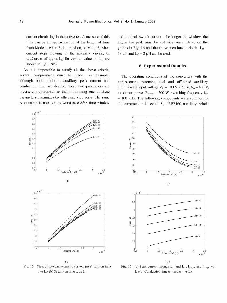
46 Journal of Power Electronics, Vol. 8, No. 1, January 2008
current circulating in the converter. A measure of this time can be an approximation of the length of time from Mode 1, when S2 is turned on, to Mode 7, when current stops flowing in the auxiliary circuit, t6, t0-6.Curves of t0-6 vs Lr2 for various values of Lr1 are shown in Fig. 17(b).
As it is impossible to satisfy all the above criteria, several compromises must be made. For example, although both minimum auxiliary peak current and conduction time are desired, these two parameters are inversely proportional so that minimizing one of these parameters maximizes the other and vice versa. The same relationship is true for the worst-case ZVS time window
and the peak switch current - the longer the window, the higher the peak must be and vice versa. Based on the graphs in Fig. 16 and the above-mentioned criteria, Lr1 = 18 µH and Lr2 = 2 µH can be used.
6. Experimental Results
The operating conditions of the converters with the non-resonant, resonant, dual and off-tuned auxiliary circuits were input voltage Vin = 100 V -250 V, Vo = 400 V, maximum power Po,max = 500 W, switching frequency fsw = 100 kHz. The following components were common to all converters: main switch S1 - IRFP460, auxiliary switch
(a)
(b)
Fig. 17 (a) Peak current through Lr1 and Lr2, ILr1,pk and ILr2,pk vs Lr2 (b) Conduction time tLr1 and tLr2 vs Lr2
(a)
(b)
Fig. 16 Steady-state characteristic curves: (a) S1 turn-on time ta vs Lr2 (b) S1 turn-on time tb vs Lr2
Circuit Properties of Zero-Voltage-Transition PWM Converters 47
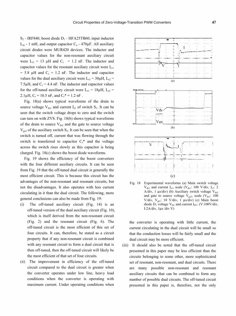
S2 - IRF840, boost diode D1 - HFA25TB60, input inductor Lin - 1 mH, and output capacitor Co - 470µF. All auxiliary circuit diodes were MUR420 devices. The inductor and capacitor values for the non-resonant auxiliary circuit were Lr1 = 13 µH and Cr = 1.2 nF. The inductor and capacitor values for the resonant auxiliary circuit were Lr1 = 5.8 µH and Cr = 1.2 nF. The inductor and capacitor values for the dual auxiliary circuit were Lr1 = 30µH, Lr2 = 7.5µH, and Cr = 4.4 nF. The inductor and capacitor values for the off-tuned auxiliary circuit were Lr1 = 18µH, Lr2 = 2.1µH, Cr = 10.5 nF, and Cr* = 1.2 nF .
Fig. 18(a) shows typical waveforms of the drain to source voltage Vds1 and current Is1 of switch S1. It can be seen that the switch voltage drops to zero and the switch can turn on with ZVS. Fig. 18(b) shows typical waveforms of the drain to source Vds2 and the gate to source voltage Vgs2 of the auxiliary switch S2. It can be seen that when the switch is turned off, current that was flowing through the switch is transferred to capacitor Cr* and the voltage across the switch rises slowly as this capacitor is being charged. Fig. 18(c) shows the boost diode waveforms.
Fig. 19 shows the efficiency of the boost converters with the four different auxiliary circuits. It can be seen from Fig. 19 that the off-tuned dual circuit is generally the most efficient circuit. This is because this circuit has the advantages of the non-resonant and resonant circuits, but not the disadvantages. It also operates with less current circulating in it than the dual circuit. The following, more general conclusions can also be made from Fig. 19: (i) The off-tuned auxiliary circuit (Fig. 14) is an
off-tuned version of the dual auxiliary circuit (Fig. 10), which is itself derived from the non-resonant circuit (Fig. 2) and the resonant circuit (Fig. 6). The off-tuned circuit is the most efficient of this set of four circuits. It can, therefore, be stated as a circuit property that if any non-resonant circuit is combined with any resonant circuit to form a dual circuit that is then off-tuned, then the off-tuned circuit will likely be the most efficient of that set of four circuits.
(ii) The improvement in efficiency of the off-tuned circuit compared to the dual circuit is greater when the converter operates under low line, heavy load conditions when the converter is operating with maximum current. Under operating conditions when
the converter is operating with little current, the current circulating in the dual circuit will be small so that the conduction losses will be fairly small and the dual circuit may be more efficient.
(iii) It should also be noted that the off-tuned circuit presented in this paper may be less efficient than the circuits belonging to some other, more sophisticated set of resonant, non-resonant, and dual circuits. There are many possible non-resonant and resonant auxiliary circuits that can be combined to form any number of possible dual circuits. The off-tuned circuit presented in this paper is, therefore, not the only
(a)
(b)
(c)
Fig. 18 Experimental waveforms (a) Main switch voltage Vds1 and current Is1, scale (Vds1: 100 V/div, Is1: 2 A/div, 1 µs/div) (b) Auxiliary switch voltage Vds2 and gate to source voltage Vgs2, scale (Vds1: 100 V/div, Vgs1: 10 V/div, 1 µs/div) (c) Main boost diode D1 voltage VD1 and current ID1: (V:100V/div, I:2A/div, 1µs /div V)
I
V
Vds
Vgs
V I

48 Journal of Power Electronics, Vol. 8, No. 1, January 2008
possible circuit of its type and another off-tuned circuit can be derived from a different combination of non-resonant and resonant auxiliary circuits. Regardless of the set of resonant, non-resonant, and dual circuits, the off-tuned circuit derived from the set will likely be the most efficient circuit of the set.
(iv) A corollary of this property would be that any of the dozens of previously proposed non-resonant auxiliary circuits can be made even more efficient if implemented with a resonant branch and then off-tuned, thus decreasing auxiliary circuit switching losses without significantly increasing auxiliary circuit conduction losses. This is especially true for non-resonant circuits as there have been considerably
more non-resonant than resonant circuits proposed and off-tuned circuits are considerably more efficient.
(v) The maximum improvement in efficiency of the off-tuned circuit when compared to the dual circuit is shown in Fig. 19. This represents the maximum gain in efficiency that can be achieved with ZVT-PWM converter structures as almost all previously proposed auxiliary circuits are non-resonant, resonant, or dual. It may be possible to achieve higher converter efficiencies, but it would take an approach that is completely different than the ZVT-PWM converter approach that has been studied for many years by power electronics experts. The efficiencies of off-tuned auxiliary circuits are probably the maximum that can be achieved with the ZVT-PWM approach in single-switch PWM converters.
(vi) As a general circuit property, the more components that an auxiliary circuit has, the more efficient it will be, but the more it will cost. It is up to a circuit designer to determine the cost benefits of one type of converter over another for his or her particular application as efficiency may be the most important factor in one application, overriding cost considerations, while cost may be the primary factor in another.
7. Conclusion
Most auxiliary circuits in single switch ZVT-PWM
converters are either non-resonant, resonant, or dual. The auxiliary switch in any non-resonant auxiliary circuit turns off with considerable current flowing through it; thus, it has switching losses that partially offset any gains in efficiency due to the reduction of turn-on losses in the main converter switch. The auxiliary switch in any resonant circuit can be made to turn off softly, but at the expense of an increase in conduction losses due to a considerable amount of circulating current flowing in the auxiliary circuit. Moreover, the main switch has a higher peak current stress than that found in conventional PWM converters as it must conduct the circulating current in the auxiliary circuit in addition to the input current. Dual auxiliary circuits combine the advantages of non-resonant and resonant auxiliary circuits so that the auxiliary switch can turn off softly as in resonant auxiliary circuits, but
86
88
90
92
94
96
100 200 300 400 500Output Power (W)
Eff. (%)
Resonant
Non-Resonant
Dual
Off-Tuned
(a)
88
90
92
94
96
98
100 125 150 175 200 225 250Input Voltage (V)
Eff. (%)
Resonant
Non-Resonant
Dual
Off-Tuned
(b)
Fig. 19 Converter efficiency (a) Efficiency vs. output power, Vin = 100 V. (b) Efficiency vs. input voltage, Po=500 W
Circuit Properties of Zero-Voltage-Transition PWM Converters 49
without the main switch peak current stress and with less circulating current. At the present time, dual circuits are the most efficient type of auxiliary circuits.
In this paper, the fundamental circuit principle of "off-tuning" was presented as a way of maximizing the efficiency of auxiliary circuits. The circulating current in dual auxiliary circuits can be reduced even further by "off-tuning" the resonant branch so that there are some auxiliary switch turn-off losses, but less than those found in non-resonant circuits. The paper reviewed the operation of auxiliary circuits in ZVT-PWM converters, and then discussed the properties and characteristics of the new off-tuned type of auxiliary circuits. There are many possible off-tuned auxiliary circuits as there are presently many previously proposed non-resonant and resonant circuits.
Experimental results obtained from 500W, 100 kHz prototype converters confirmed the feasibility of a ZVT-PWM boost converter operating with an experimental off-tuned auxiliary circuit and a comparison was made between the experimental circuit and the original non-resonant, resonant, and dual circuits from which it was derived. Based on this comparison, several general circuit properties were determined. It was concluded that an off-tuned circuit will be the most efficient circuit of the set of non-resonant, resonant, and dual circuits from which it was derived, but it also has the most components. It is up to a circuit designer to determine the cost benefits of one type of converter over another for his or her particular application.
References [1] R. Streit and D. Tollik, “A high efficiency telecom rectifier
using a novel soft-switching boost-based input current shaper,” in IEEE INTELEC Conf. Rec., 1991, pp. 720-726.
[2] G. Hua, C.-S. Leu, Y. Jiang, and F. C. Lee, “Novel zero-voltage transition PWM Converters,” in IEEE Trans. on Power Elec., vol. 9, no. 4, pp. 213-219, Mar. 1994.
[3] L. Yang and C. Q. Lee, “Analysis and Design of Boost Zero-Voltage-Transition PWM Converter”, in IEEE APEC Conf. Rec.,1993, pp.707-713.
[4] J. Gegner and C. Q. Lee, “Zero-voltage-transition converters using an inductor feedback technique," in IEEE APEC. Conf. Rec., 1994, pp. 862-868.
[5] K. M. Smith, Jr. and K. M. Smedley, “A comparison of voltage-mode soft-switching methods for PWM converters," in IEEE Trans. on Power Elec., vol. 12, no. 2, pp. 376-386, Mar. 1997.
[6] C.-J Tseng and C.-L.Chen, “Novel ZVT-PWM converter with active snubbers”, in IEEE Trans. on Power Elec., vol. 13, no. 5, pp. 861-869, Sept. 1998.
[7] G. Moschopoulos, P. Jain, G. Joos, and Y.-F. Liu, “Zero voltage switched PWM boost converter with an energy feedforward auxiliary circuit”, in IEEE Trans. on Power Elec., vol. 14, no. 4, pp. 653-662, July 1999.
[8] T.-W. Kim, H.-S. Kim, and H.-W. Ahn, “An improved ZVT PWM boost converter”, in IEEE PESC. Conf. Rec., 2000, pp. 615-619.
[9] J.-H. Kim, D. Y. Lee, H. S. Choi, and B. H. Cho, "High performance boost PFP (power factor preregulator) with an improved ZVT (zero voltage transition) converter," in IEEE APEC Conf. Rec., 2001, pp. 337-342.
[10] N. Jain, P. K. Jain, and G. Joos, “A zero voltage transition boost converter employing a soft switching auxiliary circuit with reduced conduction losses”, in IEEE Trans. on Power Elec., vol. 19, no. 1, pp. 130-139, Jan. 2004.
[11] M. L. Martins, H. A. Grundling, H. Pinheiro, and J. R. Pinheiro, and H. L. Hey, "A ZVT PWM boost converter using an auxiliary resonant source," in IEEE APEC Conf. Rec., 2002, pp. 1101-1107.
[12] C.-M. Wang, "Novel zero-voltage-transition PWM dc-dc converters" in IEEE Trans. on Ind. Elec., vol. 53, no. 1, pp. 254-262, Feb. 2006.
[13] W. Huang and G. Moschopoulos, “A new family of zero-voltage-transition PWM converters with dual active auxiliary circuits,” in IEEE Trans. on Power Elec., vol. 21, no. 2, pp. 370-379, Mar. 2006.
[14] M. L. Martins, J. L. Russi, and H. L. Hey, "Zero-voltage-transition PWM converters: a classification methodology" in IEE Proc. Elec. Power Appl., vol. 152, no. 2, pp. 323-334, Mar. 2005.
Amir Ostadi received a B.Sc. degree from Sharif University of Technology, Tehran, Iran, in Electrical Engineering. Currently, he is working towards his M.Sc. degree in Electrical Engineering, at the University of Western Ontario, London, Ontario, Canada.
His research interests include wind power generation, application of power electronics in power systems, power system restructuring, and power system stability.
50 Journal of Power Electronics, Vol. 8, No. 1, January 2008
Xing Gao received the M.E.Sc degree in Electrical & Computer Engineering from University of Western Ontario, London, Canada in 2006. He also received the M.E.Sc degree and the B. Eng degree with distinction from University of Inner Mongolia, China in
1985 and 1982 respectively. He has been a power electronics design engineer for many years in Canada and in the United States. He is currently working in Boston, US as a senior design engineer.
Gerry Moschopoulos received the Bachelor of Engineering, Master's of Applied Science and Ph.D degrees from Concordia University in Montreal, Quebec, Canada in 1989, 1992, and 1997 respectively. From 1996 to 1998, he was a design engineer in the Advanced
Power Systems division of Nortel Networks in Lachine, Quebec, Canada, working on developing power supplies and systems for telecom applications. From 1998 to 2000, he was a research engineer at Concordia University working on power converter operating with soft-switching and active power factor correction. Since 2000, he has been with the Department of Electrical and Computer Engineering at the University of Western Ontario in London, Ontario, Canada, where he is presently an associate professor. He is also a member of the Professional Engineers of Ontario