Modular Multilevel Cascade Converters without Common DC ...
11
ISSN (Print) : 2320 – 3765 ISSN (Online): 2278 – 8875 International Journal of Advanced Research in Electrical, Electronics and Instrumentation Engineering (An ISO 3297: 2007 Certified Organization) Vol. 5, Issue 11, November 2016 Copyright to IJAREEIE DOI:10.15662/IJAREEIE.2016.0511034 8488 Modular Multilevel Cascade Converters without Common DC-Link Capacitor in a Grid-Level High-Power BTB (Back-To-Back) System Y.V.J.Paul Assistant Professor, Dept. of EEE, Christu Jyoti Institute of Technology & Science, Jangaon, Telangana, India ABSTRACT: This paper provides an intensive analysis and simulation of a back-to back (BTB) system unifying two modular multilevel cascade converters based on double-star chopper cells (MMCCs-DSCCs). Each of the two DSCCs connected back-to-back consists of multiple cascaded chopper cells and a center-tapped inductor per leg. Low voltage steps bring significant reductions in harmonic voltage and current to the BTB system. Neither dc-link capacitor nor voltage sensors required for regulating the dc-link voltage and controlling the dc-link current. A three-phase downscaled BTB system with phase-shifted PWM is simulated to verify its operating principles and performance. Simulated results are obtained in steady state and transient states. In transient state simulated waveforms are obtained for step change in active power effectively KEYWORDS: back-to-back (BTB) systems, grid-connected power converters, modular multilevel cascade converters (MMCCs). I.INTRODUCTION The modular multilevel cascade converter (MMCC) family consists of several members with different given names. These members have the common family name “MMCC” because they are characterized by cascade connections of either single-phase full-bridge (H-bridge) ac/dc converters called simply as “bridge-cells” or no isolated bidirectional dc/dc choppers called just as “chopper cells.” The “double-star chopper cells (DSCCs)” used for grid connections and motor drives. Although the full name is “MMCC-DSCC,” this thesis calls it simply as a “DSCC”. The DSCC is the same in circuit configuration as a specific modular multilevel converter (MMC). A difference exists in dc- link voltage between a long-distance DSCC-based HVDC system and a DSCC-based BTB system. The HVDC system has, or will have, a dc-voltage range of 250 to 500 kV or higher to reduce the conducting power loss of overhead transmission lines and underground or undersea cables. On the other hand, the BTB system is more flexible in dc-link voltage design than the HVDC system because theft system can be considered as a “zero-meter-long” HVDC system. Therefore, it would be reasonable and acceptable forth BTB system to have a dc-link voltage as low as 66 kV or 132 kV. Another difference exists in control strategy between the HVDC and BTB systems. It lies in whether “real-time communications” between the two DSCCs are available or not. Theft system can detect actual voltages and currents in the two DSCCs and can send the detected signals to a unified digital controller because the two DSCCs are installed at the same site. The two DSCCs can be considered as a single power conversion system with the unified digital controller. The HVDC system has a digital controller for each DSCC, in which the two digital controllers are operated independent of each other because one DSCC is too far away from the other to bring the unified digital controller to the HVDC system. The two DSCCs can be considered as two separate power conversion systems. Therefore, the two DSCCs forming the BTB system can take the equal responsibility for regulating the dc-link voltage and controlling the dc-link current, whereas the two DSCCs forming the HVDC system should take different responsibilities. The “phase-shifted PWM” with the same triangular-carrier frequency as 450 Hz is applied to the two DSCCs that are the same in circuit and control. This means that simulation is reliable enough to look into more practical systems and fault-ride-through (FRT) performance. Modelling and analysis are done for the single power conversion system unifying the two DSCCs that take the equal responsibility for regulating the dc-link voltage and controlling the dc-link current.. This paper presents simulated waveforms in another transient state, where it takes 20
-
Upload
khangminh22 -
Category
Documents
-
view
1 -
download
0
Transcript of Modular Multilevel Cascade Converters without Common DC ...
ISSN (Print) : 2320 – 3765 ISSN (Online): 2278 – 8875
International Journal of Advanced Research in Electrical,
Electronics and Instrumentation Engineering (An ISO 3297: 2007 Certified Organization)
Vol. 5, Issue 11, November 2016
Copyright to IJAREEIE DOI:10.15662/IJAREEIE.2016.0511034 8488
Modular Multilevel Cascade Converters without Common DC-Link Capacitor in a
Grid-Level High-Power BTB (Back-To-Back) System
Y.V.J.Paul
Assistant Professor, Dept. of EEE, Christu Jyoti Institute of Technology & Science, Jangaon, Telangana, India
ABSTRACT: This paper provides an intensive analysis and simulation of a back-to back (BTB) system unifying two modular multilevel cascade converters based on double-star chopper cells (MMCCs-DSCCs). Each of the two DSCCs connected back-to-back consists of multiple cascaded chopper cells and a center-tapped inductor per leg. Low voltage steps bring significant reductions in harmonic voltage and current to the BTB system. Neither dc-link capacitor nor voltage sensors required for regulating the dc-link voltage and controlling the dc-link current. A three-phase downscaled BTB system with phase-shifted PWM is simulated to verify its operating principles and performance. Simulated results are obtained in steady state and transient states. In transient state simulated waveforms are obtained for step change in active power effectively KEYWORDS: back-to-back (BTB) systems, grid-connected power converters, modular multilevel cascade converters (MMCCs).
I.INTRODUCTION
The modular multilevel cascade converter (MMCC) family consists of several members with different given
names. These members have the common family name “MMCC” because they are characterized by cascade connections of either single-phase full-bridge (H-bridge) ac/dc converters called simply as “bridge-cells” or no isolated bidirectional dc/dc choppers called just as “chopper cells.” The “double-star chopper cells (DSCCs)” used for grid connections and motor drives. Although the full name is “MMCC-DSCC,” this thesis calls it simply as a “DSCC”. The DSCC is the same in circuit configuration as a specific modular multilevel converter (MMC). A difference exists in dc-link voltage between a long-distance DSCC-based HVDC system and a DSCC-based BTB system. The HVDC system has, or will have, a dc-voltage range of 250 to 500 kV or higher to reduce the conducting power loss of overhead transmission lines and underground or undersea cables. On the other hand, the BTB system is more flexible in dc-link voltage design than the HVDC system because theft system can be considered as a “zero-meter-long” HVDC system. Therefore, it would be reasonable and acceptable forth BTB system to have a dc-link voltage as low as 66 kV or 132 kV. Another difference exists in control strategy between the HVDC and BTB systems. It lies in whether “real-time communications” between the two DSCCs are available or not. Theft system can detect actual voltages and currents in the two DSCCs and can send the detected signals to a unified digital controller because the two DSCCs are installed at the same site. The two DSCCs can be considered as a single power conversion system with the unified digital controller. The HVDC system has a digital controller for each DSCC, in which the two digital controllers are operated independent of each other because one DSCC is too far away from the other to bring the unified digital controller to the HVDC system. The two DSCCs can be considered as two separate power conversion systems. Therefore, the two DSCCs forming the BTB system can take the equal responsibility for regulating the dc-link voltage and controlling the dc-link current, whereas the two DSCCs forming the HVDC system should take different responsibilities.
The “phase-shifted PWM” with the same triangular-carrier frequency as 450 Hz is applied to the two DSCCs that are the same in circuit and control. This means that simulation is reliable enough to look into more practical systems and fault-ride-through (FRT) performance. Modelling and analysis are done for the single power conversion system unifying the two DSCCs that take the equal responsibility for regulating the dc-link voltage and controlling the dc-link current.. This paper presents simulated waveforms in another transient state, where it takes 20
ISSN (Print) : 2320 – 3765 ISSN (Online): 2278 – 8875
International Journal of Advanced Research in Electrical,
Electronics and Instrumentation Engineering (An ISO 3297: 2007 Certified Organization)
Vol. 5, Issue 11, November 2016
Copyright to IJAREEIE DOI:10.15662/IJAREEIE.2016.0511034 8489
ms (one cycle at the line frequency) to reverse power flow direction at aerated power of 10 kW. Such an extremely fast response enables to enhance transient system stability as well as frequency regulation capability in some contingency situations.
II. SYSTEM CONFIGURATION
Interconnection of asynchronous networks via back-to-back HVDC links with voltage source converters (VSC) rather than conventional line-commutated or phase-commutated converters (PCC) has several system advantages. Advanced VSC technology with pulse-width modulation (PWM) permits rapid, independent control of active and reactive power in all four quadrants. Control of both active and reactive power is bi-directional and continuous across the entire operating range. Reactive power control capability allows each VSC converter to act as a Static Synchronous Compensator (STATCOM) to regulate the ac voltage at either terminal independently. Converters can be located at points in the network with relatively low short circuit levels minimizing the need for network reinforcements or remedial measures. The converters can even serve passive load should it become isolated. In such a case, the converters would control the voltage and frequency until the network is restored. Modern industrial motor drive technology has mostly migrated from PCC based systems to voltage source converter (VSC) based systems. VSC technology requires use of gate turn-off switching devices. Gate turn-off devices with higher switching frequency capability, such as the IGBT, permit more sophisticated VSC control and simpler circuit configuration by taking advantage of pulse width modulation (PWM) technique. A VSC can be controlled to synthesize an ac sinusoidal voltage by switching between different fixed dc voltage levels. By changing the PWM pattern, the phase angle, frequency and magnitude of the ac voltage can be controlled. The maximum pole-to-ground dc voltage is based on the maximum virtual converter phase-to-ground voltage. Grid-Tie Inverter:A grid-tie inverter is a power inverter that converts direct current (DC) into alternating current (AC) with an ability to synchronize to interface with a utility line. Its applications are converting DC sources such as solar panels or small wind turbines into AC for tie (synchronizing) with the grid. Residences and businesses that have a grid-tied electrical system are permitted in many countries to sell their energy to the utility grid. Electricity delivered to the grid can be compensated in several ways. "Net metering" is where the entity that owns the renewable energy power source receives compensation from the utility for its net outflow of power. So for example, if during a given month a power system feeds 500 kilowatt-hours into the grid and uses 100 kilowatt-hours from the grid, it would receive compensation for 400 kilowatt-hours. The net metering policies vary by jurisdiction. Another policy is a feed-in tariff, where the producer is paid for every kilowatt hour delivered to the grid by a special tariff based on a contract with Distribution Company or other power authority. The grid-interactive power systems are covered by specific provisions which also mandate certain requirements for grid-interactive inverters. Back to Back System : A back-to-back station (BTB) is a plant in which both converters are in the same area, usually in the same building. Bidirectional power flow capability is available and to meet high demand from surplus power available in either regions. The length of the direct current line is kept as short as possible. HVDC back-to-back stations are used for coupling of electricity grids of different frequencies ,coupling two networks of the same nominal frequency but no fixed phase relationship ,different frequency and phase number (for example, as a replacement for traction current converter plants). The DC voltage in the intermediate circuit can be selected freely at HVDC back-to-back stations because of the short conductor length. The DC voltage is usually selected to be as low as possible, in order to build a small valve hall and to reduce the number of thyristors connected in series in each valve. For this reason, at HVDC back-to-back stations, valves with the highest available current ratings are used.
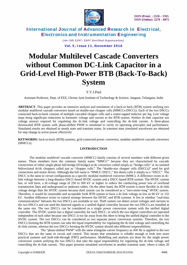
High-power BTB and long-distance HVDC systems have the capability of executing asynchronous interties between two power transmission grids with the same line frequency as 50 Hz. The function of asynchronous intertie to the two grids is to make bidirectional power-flow control independent of a phase difference between the sending grid voltage and the receiving grid voltage. When the line frequencies of the two grids are different, that is, 50 Hz, the BTB system is referred to as a frequency changer (FC). Fig. 1 shows a feasible circuit configuration of a DSCC based BTB system for power transmission grids. The power capacity of the BTB system is rated at 200 MW. The secondary line-to-line voltage of each line-frequency transformers designed as 66 kV, and the dc-link voltage between the two DSCCs is set to 132 kV, as shown in Fig. 1.
ISSN (Print) : 2320 – 3765 ISSN (Online): 2278 – 8875
International Journal of Advanced Research in Electrical,
Electronics and Instrumentation Engineering (An ISO 3297: 2007 Certified Organization)
Vol. 5, Issue 11, November 2016
Copyright to IJAREEIE DOI:10.15662/IJAREEIE.2016.0511034 8490
Fig. 1 Circuit configuration of the 200-MW DSCC-based BTB (FC) system
As an example, the BTB system is assumed to adopt the 6-kV GCTs (gate commutated thyristors), and the dc-
capacitor reference voltage of each chopper cell is assumed to be 3 kV. When the count of chopper cells per leg results in 88 (= 2×132kV/3kV), the BTB system has the following advantages. Each chopper cell is equipped with a floating dc capacitor and a dc voltage sensor, but without auxiliary dc-voltage balancing circuit or start-up circuit. Since multilevel waveforms with low voltage steps can be considered almost sinusoidal, the line current gets purely sinusoidal at unity power factor or with any power factor controllable. As a result, the BTB system requires neither harmonic filter nor capacitor for power factor correction, unlike a conventional current-source BTB system using line-commutated thyristors. The sinusoidal voltage and current allow the BTB system to use a three-phase conventional and simple line frequency transformer for voltage matching and galvanic isolation between 500 kV and 66 kV. No ac-link inductor is required because it can be replaced by the intentionally increased leakage inductance of the transformer. No dc-link high-voltage capacitor is required between the two DSCCs because the floating dc capacitor of each chopper cell acts as an energy buffer. Therefore, neither additional cost nor volume is required for installing the dc-link high-voltage capacitor. No dc-link voltage sensor is required because an indirect feedback control loop makes it possible to indirectly regulate the mean dc-link voltage to its reference. This control loop is based on the signals obtained from the dc voltage sensors installed across the floating dc capacitors of all the chopper cells.
III. CIRCUIT CONFIGURATION
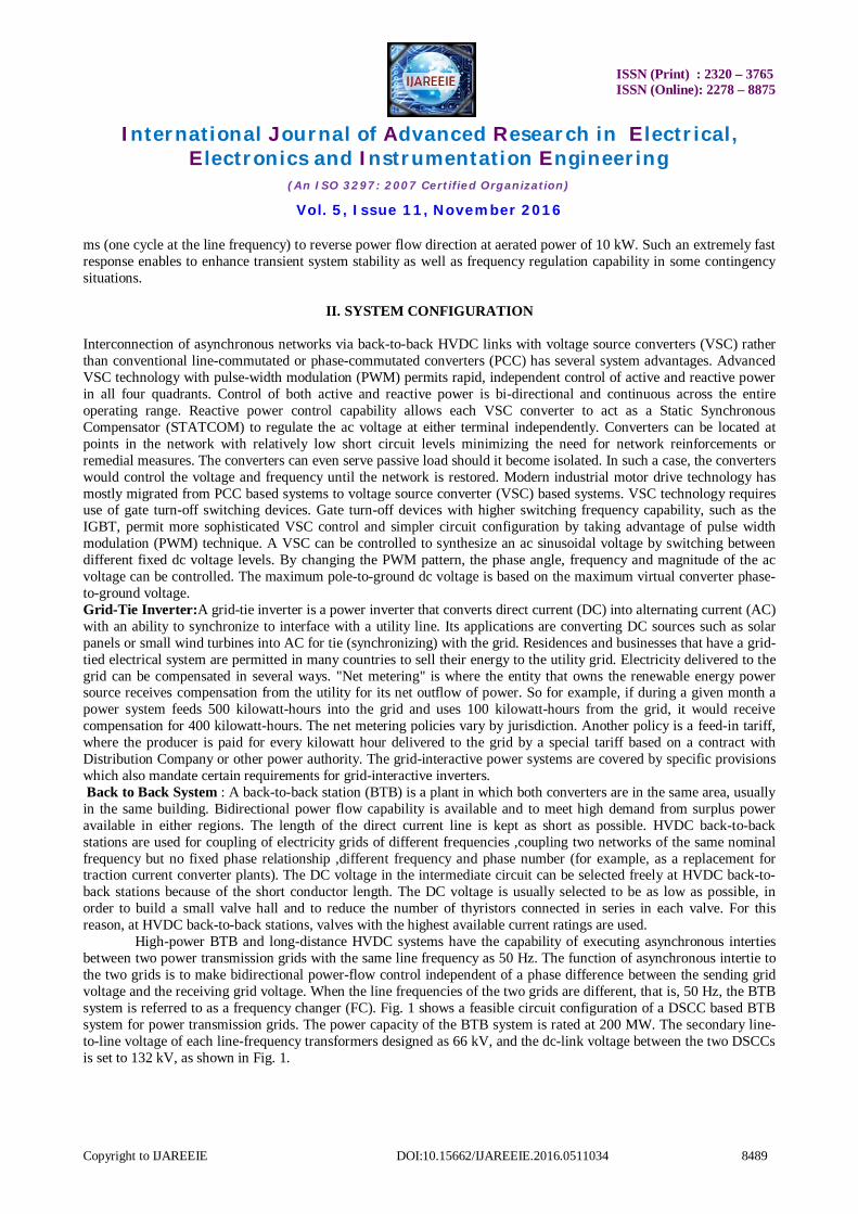
The power circuit configuration of the DSCC based BTB system with a per-leg chopper-cell count of 16 is
shown in fig 2 couple of identical DSCCs, “DSCC-A” and “DSCC-B” are connected back-to-back without any common dc-link capacitor. Each DSCC consists of 48 chopper cells depicted in Fig. 3(a) and three center-tapped inductors in Fig. 3(b). Here, LZ is not the inductance between the center tap and another node P or N but the inductance between two nodes P and N. In Fig. 2, iPuA and iNuA are the positive and negative arm currents, iSuA is the supply current, and iZuA is the circulating current
Fig 2 Circuit configuration of the DSCC-based BTB system with 16 chopper cells per leg.
ISSN (Print) : 2320 – 3765 ISSN (Online): 2278 – 8875
International Journal of Advanced Research in Electrical,
Electronics and Instrumentation Engineering (An ISO 3297: 2007 Certified Organization)
Vol. 5, Issue 11, November 2016
Copyright to IJAREEIE DOI:10.15662/IJAREEIE.2016.0511034 8491
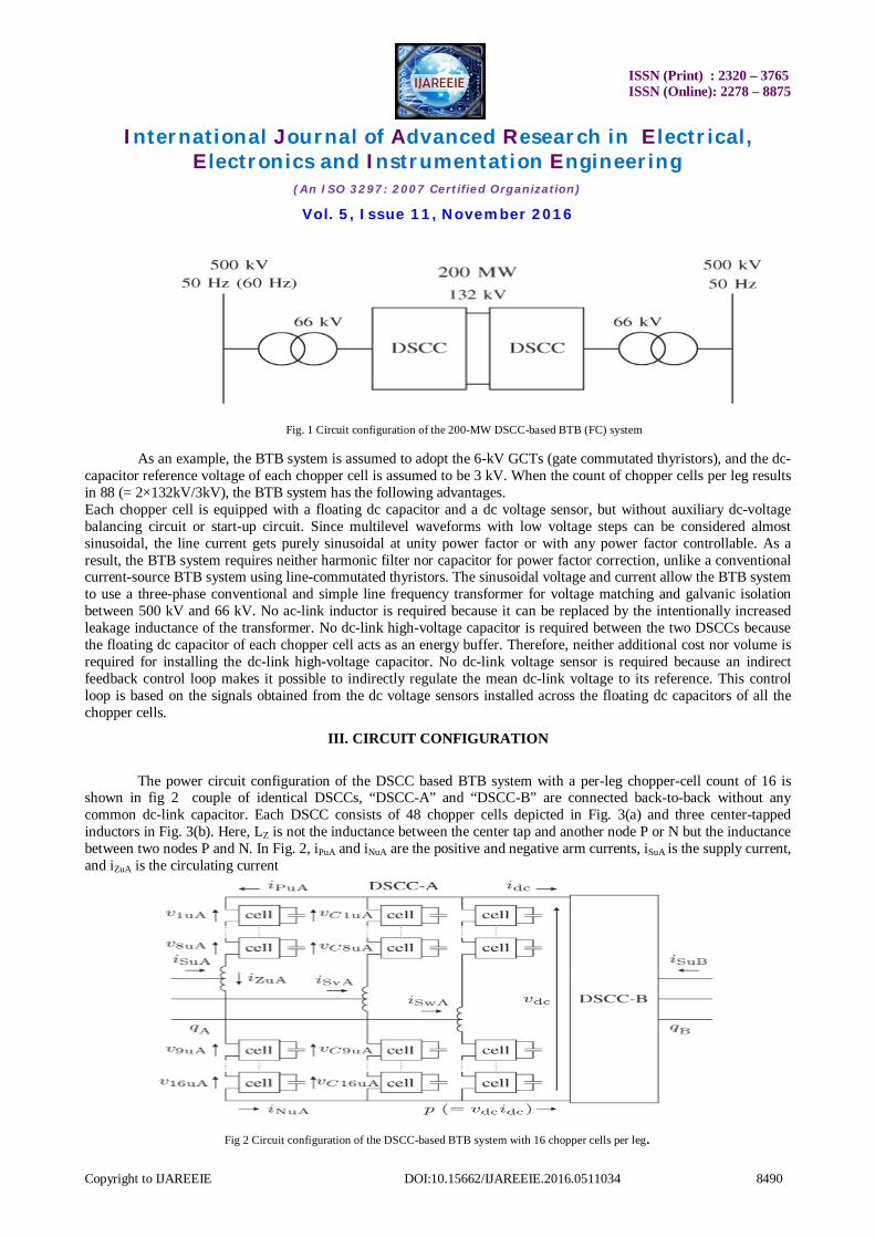
The chopper cell in Fig 3. 2(b) is a non-isolated “bidirectional” dc/dc converter. Since two pairs of dc terminals considered as either input or output, it is referred as “low-voltage side” and “high voltage side” because the dc voltage across one pair, to which a dc capacitor is connected, is always higher than the mean dc voltage across the other pair.
Fig 3 (a) Chopper cell. Fig 3 (b) Center-tapped inductor.
Along the u-phase leg of DSCC-A iZuA is given by
iZuA = (iPuA + iNuA) (1)
The count of independent variables out of the three branch currents iPuA ,iNuA and iSuA is not three but two because of Kirchhoff’s current law at the u-phase ac-terminal of DSCC-A or at the center tap of the u-phase center tapped inductor. The supply current and the circulating current are selected as two independent variables. The positive and negative arm currents are expressed as dependent variables as follows
iPuA =− + iZuA (2)
iNuA = + iZuA (3) The first terms of the right-hand sides in (2) and (3) are related to the supply current. They are out of phase by 1800 with each other. Therefore, the magnetic fluxes formed by the supply current cancel out each other inside the magnetic core of the center-tapped inductor. As a result, the inductor presents no inductance to the supply current, whereas it renders the inductance LZ to the circulating current
Each DSCC has16 chopper cells per leg. The dc reference voltage of each floating capacitor is set to v∗C=50V, so that the dc-link reference voltage should be set to v∗dc= 400V. Each triangular-carrier frequency is set at fc= 450Hz, and a dead or blanking times 8μs. The 16 triangular-carrier signals phase-shifted one another by 22.50 (= 360◦/16). Three phase nominal line-to-line rams voltages of 66 kV and 200 V in the practical and downscaled systems are typical high-voltage transmission and low-voltage distribution voltages respectively. The unit capacitance constant of the dc capacitors, HC is defined by
HC = VC2 (4)
The energy stored in all the dc capacitors, to which the rated voltage is applied, is divided by the rated power of the converter. SI unit of HC is J/W=S. The unit capacitance constant is useful and effective in designing dc capacitors and in comparing dc capacitors in one BTB system to another one with different voltage and current ratings. The reason is that the unit capacitance constant can be considered as a kind of per-unit value although per-unit values have no physical unit. BTB Operation Modes: The BTB is designed to operate in two control modes. The primary mode is reactive power support for voltage control of the bus and the secondary mode is active power flow. In voltage control mode, the BTB operates with a control slope to supply reactive power for voltage support. To transfer power in either direction the BTB operates in power control mode, it will continue to transfer power if the voltage is within a dead-band. For conditions outside the dead-band the BTB operates in Voltage control mode. The dead-band is designed so that local capacitor switching or changes in remote generation which cause slight voltage swings do not cause the BTB to switch to voltage control mode. The BTB can perform many functions dictated by the operating configurations of the two VSCs. The following are the major operating configurations for the BTB. Voltage Control Mode in this mode, the BTB can provide independent voltage control to both the systems. The BTB provides the required reactive power support on both sides to maintain a pre-set voltage. Active power can be transferred from either side while maintaining a constant voltage on the two systems. Any active power transfers that are scheduled are automatically and instantaneously lowered if needed by the control system to supply the needed reactive power support to maintain a constant voltage. Active Power Control Mode In active power mode, the BTB provides active power transfer between the systems. It then allows power transfer when the voltage is within a dead-band. If the voltage goes
ISSN (Print) : 2320 – 3765 ISSN (Online): 2278 – 8875
International Journal of Advanced Research in Electrical,
Electronics and Instrumentation Engineering (An ISO 3297: 2007 Certified Organization)
Vol. 5, Issue 11, November 2016
Copyright to IJAREEIE DOI:10.15662/IJAREEIE.2016.0511034 8492
beyond this dead-band the BTB automatically goes into voltage control mode. The active power flow is then automatically and instantaneously lowered by the BTB as needed to provide the required reactive power support
Independent Operation Mode of the two VSCs Should be maintained as required on one side of the BTB, the other side can still provide voltage control to either side of the BTB. This is done by opening the DC bus to split it into two halves. As the DC link is open, no active power can be transferred between the two sides of the BTB for this configuration. Each VSC will then be capable of providing up to +36 MVAR of reactive support to either side. The BTB can provide voltage control to the load if it is transferred to the other power system. The BTB in this configuration would be capable of supplying +72 MVAR of reactive support to the system supplying the power. As the bypass breaker has to be closed in this configuration, no active power can be transferred via the BTB.
DC current component these components has a DC (or positive average) current through the source is essential to have a "real power" delivered from the DC source to the load. If this dc component did not exist no power could be transferred from the dc source. This DC current is charging the capacitors in the modules. If the module capacitors are replaced by ideal voltage sources no DC current component flows through the DC source as the module ideal sources are powering the load. AC current component these are primarily a 2nd order harmonic component (e.g. 100Hz) which is responsible for charging an AC fluctuation offset by the DC current component. This is derived from the charging and discharging of the module capacitors while they are inserted and bypassed approximately twice per fundamental current cycle. If the module capacitors are replaced by ideal voltage sources 2nd harmonic will still be present in the circulating current as it is the result of the switching function. Load current this is a current component shared by the upper and the lower converter arms and adding at the load branch. The circulating current is essential to secure equal charging and discharging of all converter module capacitors so that each of them has a constant average DC voltage across it. The circulating current through the DC source is reduced progressively with an increasing number of converter legs.
IV. CONTROL TECHNIQUES
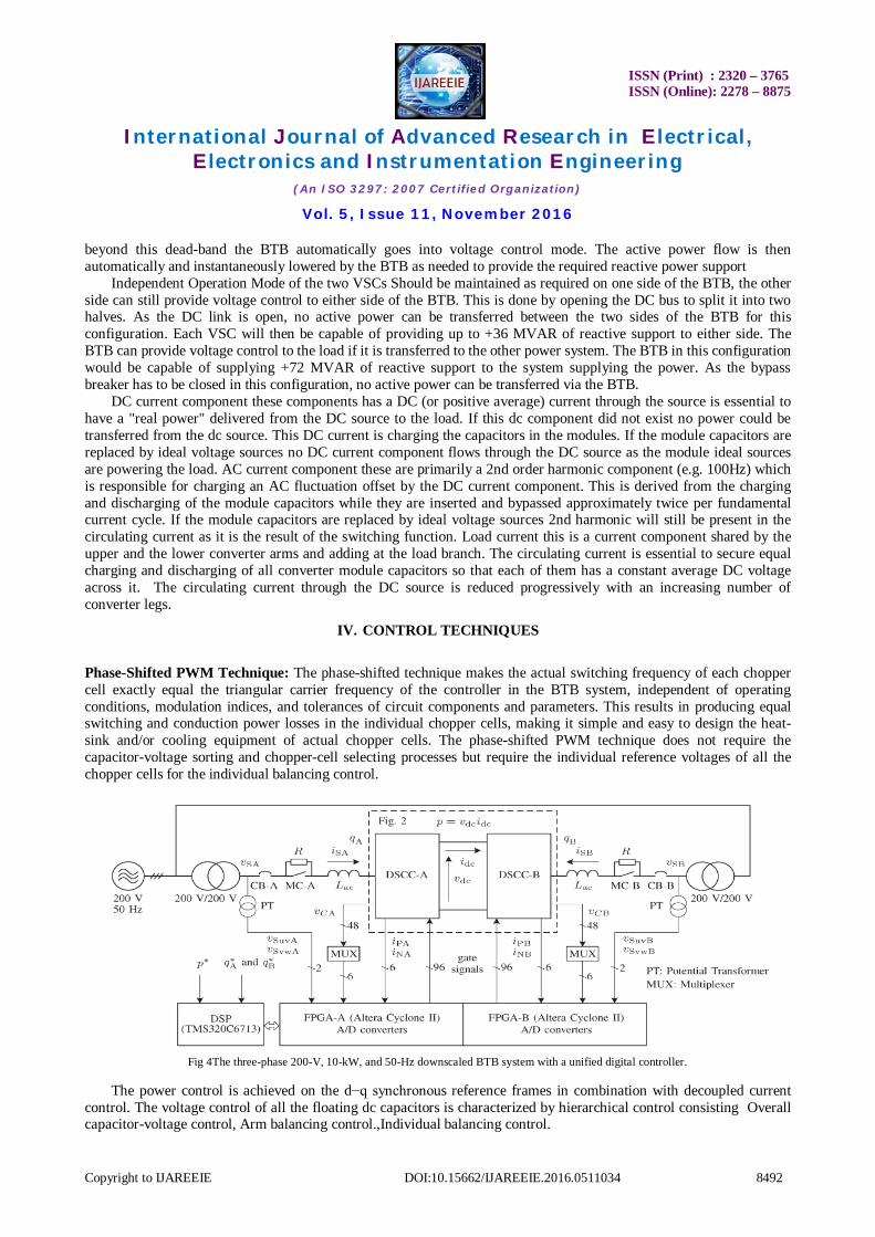
Phase-Shifted PWM Technique: The phase-shifted technique makes the actual switching frequency of each chopper cell exactly equal the triangular carrier frequency of the controller in the BTB system, independent of operating conditions, modulation indices, and tolerances of circuit components and parameters. This results in producing equal switching and conduction power losses in the individual chopper cells, making it simple and easy to design the heat-sink and/or cooling equipment of actual chopper cells. The phase-shifted PWM technique does not require the capacitor-voltage sorting and chopper-cell selecting processes but require the individual reference voltages of all the chopper cells for the individual balancing control.
Fig 4The three-phase 200-V, 10-kW, and 50-Hz downscaled BTB system with a unified digital controller.
The power control is achieved on the d−q synchronous reference frames in combination with decoupled current
control. The voltage control of all the floating dc capacitors is characterized by hierarchical control consisting Overall capacitor-voltage control, Arm balancing control.,Individual balancing control.
ISSN (Print) : 2320 – 3765 ISSN (Online): 2278 – 8875
International Journal of Advanced Research in Electrical,
Electronics and Instrumentation Engineering (An ISO 3297: 2007 Certified Organization)
Vol. 5, Issue 11, November 2016
Copyright to IJAREEIE DOI:10.15662/IJAREEIE.2016.0511034 8493
The overall capacitor-voltage control in the top layer takes the responsibility for regulating the arithmetical average voltage of all the dc capacitors to its reference. Adjusting a small amount of active power supplied from the ac mains makes it Possible to regulate the arithmetical average voltage of all the capacitors to its reference. The adjusted active power corresponds to the whole power loss of the two DSCCs. This control results in producing a slight difference in active power between each ac side and the dc link.The arm-balancing control in the middle layer plays an important role in balancing 12 arithmetical average voltages, each of which is the arithmetical average voltage of eight dc capacitors per arm. The dc component of the circulating current in each leg is adjusted to exchange a small amount of active power among the six legs while fundamental (50 Hz) component is used for the adjustment of an active-power difference between the positive and negative arms. No circulating current flows in the SSBC (single-star bridge cells)- whereas the circulating currents flowing in the DSCC can be controlled independently .The individual balancing control in the bottom layer takes charge of regulating each dc-capacitor voltage to the arithmetical average voltage of eight dc capacitors per arm. This straightforward control adjusts the active power formed by the low-voltage-side voltage of each chopper cell and the arm current. The combination of the phase-shifted PWM technique with the voltage control of all the dc capacitors imposes no limitation on the number of cascaded chopper cells per leg theoretically. Control of dc-Link Voltage and current: The dc-link voltage and current control considering the two DSCCs as a unified power conversion system.
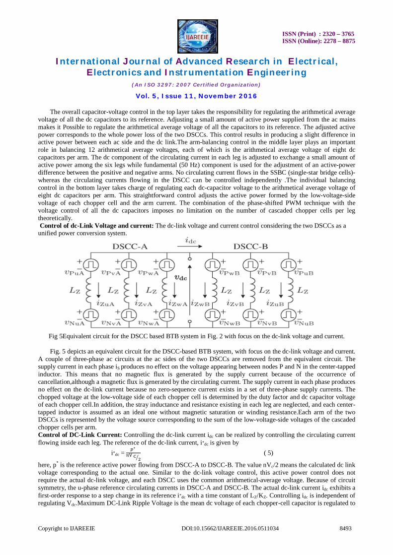
Fig 5Equivalent circuit for the DSCC based BTB system in Fig. 2 with focus on the dc-link voltage and current.
Fig. 5 depicts an equivalent circuit for the DSCC-based BTB system, with focus on the dc-link voltage and current.
A couple of three-phase ac circuits at the ac sides of the two DSCCs are removed from the equivalent circuit. The supply current in each phase iS produces no effect on the voltage appearing between nodes P and N in the center-tapped inductor. This means that no magnetic flux is generated by the supply current because of the occurrence of cancellation,although a magnetic flux is generated by the circulating current. The supply current in each phase produces no effect on the dc-link current because no zero-sequence current exists in a set of three-phase supply currents. The chopped voltage at the low-voltage side of each chopper cell is determined by the duty factor and dc capacitor voltage of each chopper cell.In addition, the stray inductance and resistance existing in each leg are neglected, and each center-tapped inductor is assumed as an ideal one without magnetic saturation or winding resistance.Each arm of the two DSCCs is represented by the voltage source corresponding to the sum of the low-voltage-side voltages of the cascaded chopper cells per arm. Control of DC-Link Current: Controlling the dc-link current idc can be realized by controlling the circulating current flowing inside each leg. The reference of the dc-link current, i∗dc is given by
i∗dc = ∗
( 5)
here, p* is the reference active power flowing from DSCC-A to DSCC-B. The value nVc/2 means the calculated dc link voltage corresponding to the actual one. Similar to the dc-link voltage control, this active power control does not require the actual dc-link voltage, and each DSCC uses the common arithmetical-average voltage. Because of circuit symmetry, the u-phase reference circulating currents in DSCC-A and DSCC-B. The actual dc-link current idc exhibits a first-order response to a step change in its reference i∗dc with a time constant of LZ/KZ. Controlling idc is independent of regulating Vdc.Maximum DC-Link Ripple Voltage is the mean dc voltage of each chopper-cell capacitor is regulated to
ISSN (Print) : 2320 – 3765 ISSN (Online): 2278 – 8875
International Journal of Advanced Research in Electrical,
Electronics and Instrumentation Engineering (An ISO 3297: 2007 Certified Organization)
Vol. 5, Issue 11, November 2016
Copyright to IJAREEIE DOI:10.15662/IJAREEIE.2016.0511034 8494
V*C and that the ac components of each capacitor are neglected. The use of a phase-shifted PWM technique makes
voltage steps equal V*C. As a result, the instantaneous value takes one out of V∗dc, V∗dc+V∗C, and V∗dc−V∗C.
V∗dc−V∗C ≤ Vdc ≤ V∗dc+V∗C (6) Theoretically, the possible maximum ripples voltage appearing across the dc link is 2V∗C in peak-to-peak. Actually, the maximum ripple voltage would be lower than, or equal to, 2V∗C.
V. RESULTS AND DISCUSSION
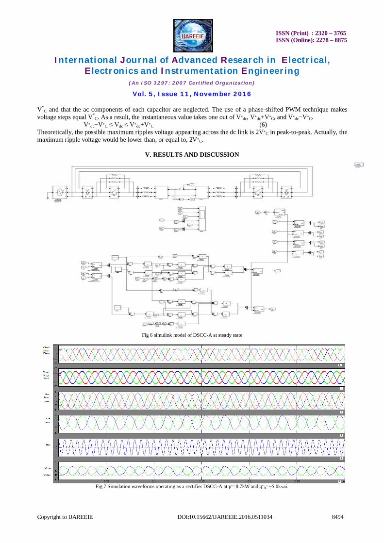
Fig 6 simulink model of DSCC-A at steady state
Fig 7 Simulation waveforms operating as a rectifier DSCC-A at p∗=8.7kW and q∗A=−5.0kvai.
ISSN (Print) : 2320 – 3765 ISSN (Online): 2278 – 8875
International Journal of Advanced Research in Electrical,
Electronics and Instrumentation Engineering (An ISO 3297: 2007 Certified Organization)
Vol. 5, Issue 11, November 2016
Copyright to IJAREEIE DOI:10.15662/IJAREEIE.2016.0511034 8495
In fig 7 supply current in DSCC-A is in phase with the corresponding supply line-to-line voltage (iSuA and VSuvA). The ac terminal line-to-line voltage Vuv is a multilevel PWM waveform containing much less harmonic voltage. The arm currents iPu and iNu contain not only dc and 50-Hz components but also a 100-Hz component originated from the dc-capacitor voltage fluctuation and switching-ripple component. The dc current included in the circulating current iZu is−7.3A in DSCC-A, Representative dc-capacitor voltagesVC1u and VC9u contain both dc and ac components, and the capacitor-voltage control regulates the dc component to its reference voltage of 50 V. The 50-Hz and 100-Hz components are proportional to the rms value of the supply currents and inversely proportional to the capacitance value of the dc capacitors.
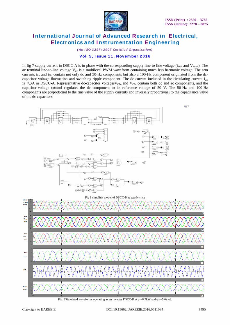
Fig 8 simulink model of DSCC-B at steady state
Fig. 9Simulated waveforms operating as an inverter DSCC-B at p∗=8.7kW and q∗B=5.0kvai.
ISSN (Print) : 2320 – 3765 ISSN (Online): 2278 – 8875
International Journal of Advanced Research in Electrical,
Electronics and Instrumentation Engineering (An ISO 3297: 2007 Certified Organization)
Vol. 5, Issue 11, November 2016
Copyright to IJAREEIE DOI:10.15662/IJAREEIE.2016.0511034 8496
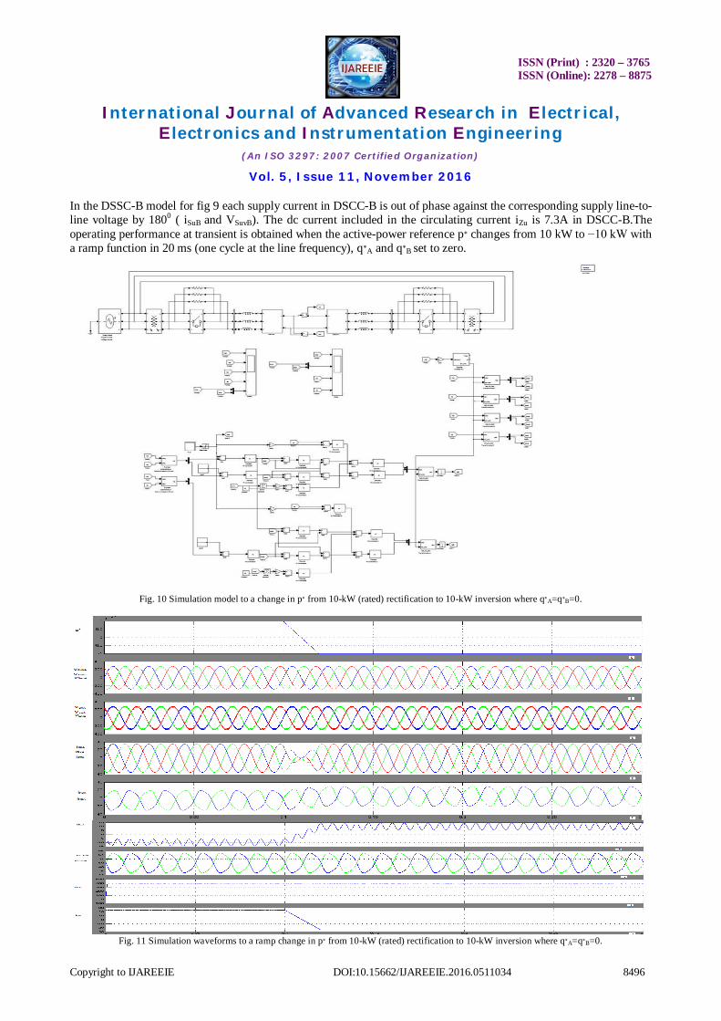
In the DSSC-B model for fig 9 each supply current in DSCC-B is out of phase against the corresponding supply line-to-line voltage by 1800 ( iSuB and VSuvB). The dc current included in the circulating current iZu is 7.3A in DSCC-B.The operating performance at transient is obtained when the active-power reference p∗ changes from 10 kW to −10 kW with a ramp function in 20 ms (one cycle at the line frequency), q∗A and q∗B set to zero.
Fig. 10 Simulation model to a change in p∗ from 10-kW (rated) rectification to 10-kW inversion where q∗A=q∗B=0.
Fig. 11 Simulation waveforms to a ramp change in p∗ from 10-kW (rated) rectification to 10-kW inversion where q∗A=q∗B=0.
ISSN (Print) : 2320 – 3765 ISSN (Online): 2278 – 8875
International Journal of Advanced Research in Electrical,
Electronics and Instrumentation Engineering (An ISO 3297: 2007 Certified Organization)
Vol. 5, Issue 11, November 2016
Copyright to IJAREEIE DOI:10.15662/IJAREEIE.2016.0511034 8497
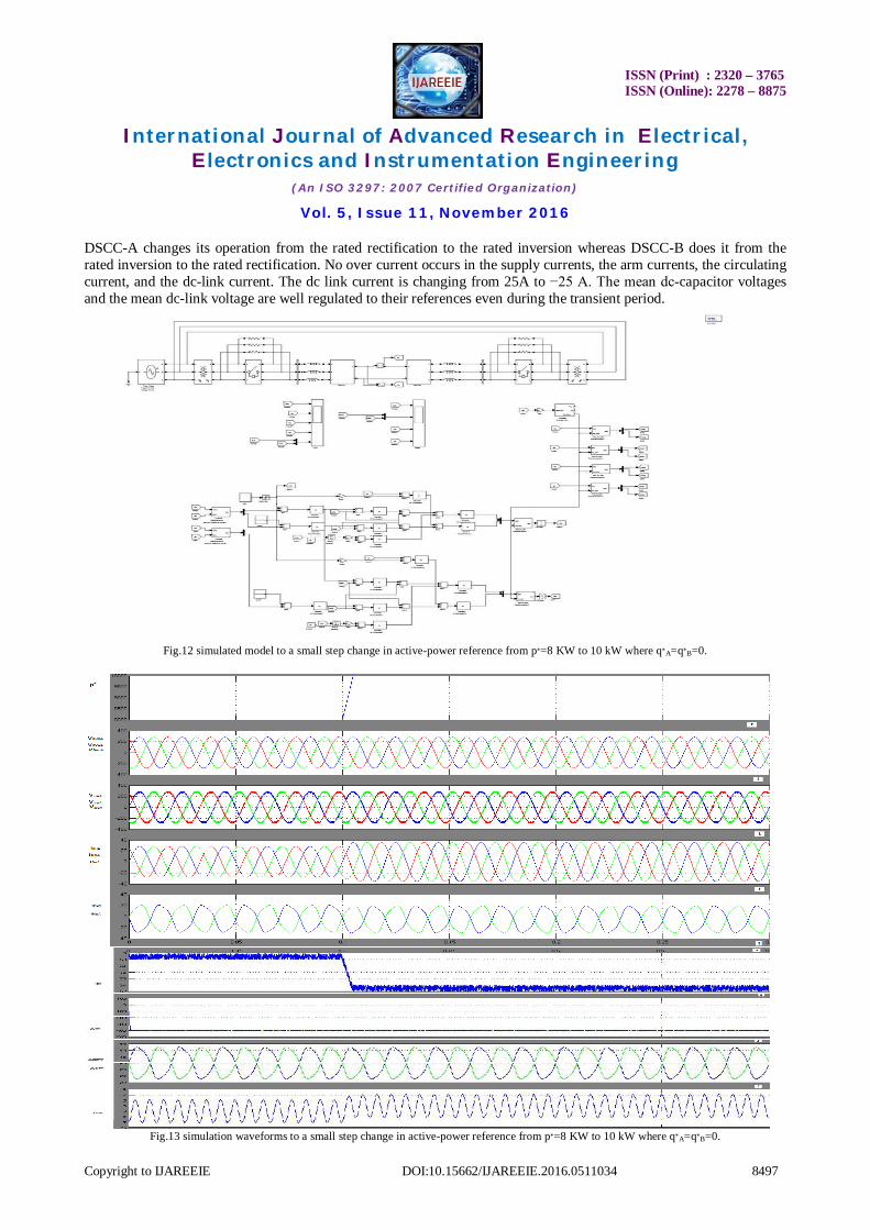
DSCC-A changes its operation from the rated rectification to the rated inversion whereas DSCC-B does it from the rated inversion to the rated rectification. No over current occurs in the supply currents, the arm currents, the circulating current, and the dc-link current. The dc link current is changing from 25A to −25 A. The mean dc-capacitor voltages and the mean dc-link voltage are well regulated to their references even during the transient period.
Fig.12 simulated model to a small step change in active-power reference from p∗=8 KW to 10 kW where q∗A=q∗B=0.
Fig.13 simulation waveforms to a small step change in active-power reference from p∗=8 KW to 10 kW where q∗A=q∗B=0.
ISSN (Print) : 2320 – 3765 ISSN (Online): 2278 – 8875
International Journal of Advanced Research in Electrical,
Electronics and Instrumentation Engineering (An ISO 3297: 2007 Certified Organization)
Vol. 5, Issue 11, November 2016
Copyright to IJAREEIE DOI:10.15662/IJAREEIE.2016.0511034 8498
The simulated waveforms to a small step change in p∗ from 8 to 10 kW, where q∗A=q∗B=0. No over current occurs in the supply currents, the arm currents, the circulating current, and the dc-link current. The dc link current is changing from 19.8A to 25 A. The mean dc-capacitor voltages and the mean dc-link voltage are well regulated to their references even during the transient period.
VI.CONCLUSION
This paper describes a grid-level high-power BTB (back to-back) system using two modular multilevel cascade converters based on double-star chopper cells (MMCC-DSCC) without common dc-link capacitor. A three-phase 200-V, 10-kW, 50-Hz BTB system with phase-shifted PWM is used to verify its operating principles and performance. Simulation waveforms are obtained for two cases steady state and transient state. The simulation program developed in this project is so reliable that it is applicable, particularly to investigations into low-voltage-ride-through (LVRT) capability and fault tolerances encountered in the operation of actual systems. Modelling and analysis have been done for the single power conversion system unifying the two DSCCs that take the equal responsibility for regulating the dc-link voltage and controlling the dc-link current. Simulation waveforms in transient state obtained when the active-power reference p∗ changes from 10 kW to −10 kW with a ramp function of one cycle at the line frequency, q∗A and q∗B set to zero shows no over current occurs in the supply currents, the arm currents, the circulating current, and the dc-link current. The dc link current is changing from 25A to −25 A. The mean dc-capacitor voltages and the mean dc-link voltage are well regulated to their references even during the transient period.
REFERENCES
[1] H. Adage, “Classification, terminology, and application of the Modular Multilevel Cascade Converter (MMCC),”IEEE Trans. Power Electron., vol. 26, no. 11, pp. 3119–3130, Nov. 2011. [2] R. Marquardt and A. Legnica, “A new modular voltage source inverter topology,” import. EPE, 2003, pp. 2–4. [3] S. Allegro, R. Hammers, and R. Marquardt, “New transformer less, scalable modular multilevel converters for HVDC-transmission,” in Proc.IEEE PESC, 2008, pp. 174–179. [4] R. Marquardt, “Modular multilevel converter: A universal concept for HVDC-networks and extended dc-bus-applications,” in Proc. IPEC, 2010, pp. 502–507. [5] J. Qin and M. Saeedifard, “Predictive control of a modular multilevel Converter for a back-to-back HVDC system,”IEEE Trans. Power Del.,vol. 27, no. 3, pp. 1538–1547, Jul. 2012. [6] M. Guan and Z. CSU, “Modeling and control of a modular multilevel Converter-based HVDC system under unbalanced grid conditions,”IEEE Trans. Power Electron. vol. 27, no. 12, pp. 4858–4867, Dec. 2012. [7] G. Bergner et al., “An energy-based controller for HVDC modular multilevel converter in decoupled double synchronous reference frame for Voltage oscillation reduction,”IEEE Trans. Ind. Electron., vol. 60, no. 6, pp. 2360–2371, Jun. 2013. [8] M. Hagiwara and H. Adage, “Control and experiment of pulsewidthmodulated modular multilevel converters,”IEEE Trans. Power Electron. vol. 24, no. 7, pp. 1737–1746, Jul. 2009. [9] M. Hagiwara, K. Nishimura, and H. Adage, “A medium-voltage motorDrive with a modular multilevel PWM inverter,”IEEE Trans. Power Electron., vol. 25, no. 7, pp. 1786–1799, Jul. 2010. [10] H. Pang, M. Hagiwara, and H. Adage, “Modeling and analysis of Switching-ripple voltage on the dc link between a diode rectifier and a Modular multilevel cascade inverter (MMCI),”IEEE Trans. Power Electron., vol. 28, no. 1, pp. 75–84, Jan. 2013. [11] M. Hagiwara, I. Hasegawa, and H. Adage, “Start-up and low-speed operation of an adjustable-speed motor driven by a modular multilevel cascadenverter (MMCI),”IEEE Trans. Ind. Appl., vol. 49, no. 4, pp. 1556–1565,Jul./Aug. 2013. [12] S. Rohmer, J. Weber, and S. Beret, “Continuous model of modular multilevel converter with experimental verification,” in Proc. IEEE ECCE, 2011, pp. 4021–4028. [13] J. Kolb, F. Kemmerer, and M. Braun, “Straight forward vector control of the modular multilevel converter for feeding three-phase machines over their complete frequency range,” in Proc. IEEE IECON, 2011,pp. 1596–1601. [14] J. Kolb, F. Kemmerer, and M. Braun, “Dimensioning and design of modular multilevel converter for drive applications,” import. EPE/PEMC, 2012, pp. LS1a-1.1-1–LS1a-1.1-8.