
Multilevel multiphase space vector PWM algorithm with switching state redundancy applied to...
8
Multilevel Multiphase Space Vector PWM Algorithm With Switching State Redundancy Applied to Three-Phase Four-Leg Converters Óscar López, Jacobo Álvarez, Francisco D. Freijedo, Alejandro G. Yepes, Jano Malvar, Pablo Fernández-Comesaña, Jesús Doval-Gandoy, Andrés Nogueiras, Alfonso Lago and Carlos M. Peñalver Electronics Technology Department University of Vigo Vigo, Spain ES-36210 Email: [email protected] Abstract—Three-phase four-leg voltage-source converters are used in inverter, rectifier and active filter applications to control the neutral current caused by unbalanced or nonlinear loads. From the modulation point of view, a four-leg converter can be considered as a four-phase system. Hence, the modulation task can be carried out with a generic multiphase modulation algorithm. In this paper, a recent multilevel multiphase space vector PWM algorithm with switching state redundancy is particularized for multilevel three-phase four-leg converters. The obtained algorithm is compared with an existing three-dimension modulation technique showing important similarities. Finally, the new algorithm is implemented in a low-cost field-programmable gate array and it is tested with a five-level cascaded full-bridge inverter. I. I NTRODUCTION In four wire systems, unbalanced or nonlinear loads and unbalanced sources can cause large neutral currents. The extra leg of four-leg converters provides an effective neutral connection which allows a precise current control [1]. The growing interest in four-leg converters for three-phase four- wire systems focuses in applications such as distributed power generation, active power filters, fault-tolerant rectifiers and common mode noise reduction. The carrier-based pulse-width modulation (PWM) can be easily applied to four-leg converters [2] even for multilevel topologies [3]. The application of the space vector pulse- width modulation (SVPWM) to four-leg converters is more involved. In fact, most of the SVPWM algorithms that have been developed to four-leg converters are devoted to two-level converters [4]–[6]. From the modulation point of view, a four-leg converter can be considered as a four-phase converter. Therefore, the general multilevel multiphase SVPWM techniques developed in [7] and [8] can be applied to solve the space vector modulation problem in four-leg converters. This paper is the last one of a series of four papers that show the application of both multiphase multilevel SVPWM techniques to three-phase converters with three and four legs [9]–[11]. The application of the multiphase modulation technique in [7] to multilevel converters with three legs provides the simple modulation al- gorithm in [9], which is fully equivalent to the previous three- dimensional (3D) SVPWM algorithm presented in [12]. If the technique in [7] is applied to multilevel four-leg converters then the result is the novel four-dimensional (4D) SVPWM algorithm presented in [10]. The modulation technique in [7] does not make use of the switching state redundancy available in multilevel converters, which allows to use different switching state combinations with the same phase-to-phase voltages but with different homopolar voltage component. Consequently, the modulation index range available with the SVPWM algorithms in [9] and [10] is not optimal and it can be extended. Such problem is solved by the multilevel multiphase SVPWM technique in [8] that takes advantage of the switching state redundancy. The application of this modulation technique to three-phase three-leg converters provides the very simple algorithm in [11] in which the part devoted to calculate the two-dimensional (2D) space vectors is equivalent to the fast 2D SVPWM algorithm presented in [13]. Consequently, the algorithm in [11] can be considered as an extension of the algorithm in [13] that includes a method to select the redundant switching states. This paper presents the application of the multilevel mul- tiphase SVPWM technique in [8] to three-phase four-leg converters. The result is a new 3D SVPWM algorithm that allows to select the switching states of the converter among the available redundant states. This new algorithm is com- pared with the existing multilevel 3D SVPWM algorithm in [14] showing important similarities. Finally, the modulation technique is implemented in a field-programmable gate array (FPGA) and it is tested with a real prototype based on a five- level cascaded full-bridge inverter. II. MULTILEVEL MULTIPHASE SVPWM ALGORITHM WITH SWITCHING STATE REDUNDANCY The SVPWM in multiphase converters is a multidimen- sional problem in which the vector selection can be carried out directly in a multidimensional space. In [8], the mod- 978-1-4244-5226-2/10/$26.00 ゥ2010 IEEE 568
-
Upload
independent -
Category
Documents
-
view
6 -
download
0
Transcript of Multilevel multiphase space vector PWM algorithm with switching state redundancy applied to...

Multilevel Multiphase Space Vector PWMAlgorithm With Switching State RedundancyApplied to Three-Phase Four-Leg Converters
Óscar López, Jacobo Álvarez, Francisco D. Freijedo, Alejandro G. Yepes, Jano Malvar,Pablo Fernández-Comesaña, Jesús Doval-Gandoy, Andrés Nogueiras, Alfonso Lago and Carlos M. Peñalver
Electronics Technology DepartmentUniversity of Vigo
Vigo, Spain ES-36210Email: [email protected]
Abstract—Three-phase four-leg voltage-source converters areused in inverter, rectifier and active filter applications to controlthe neutral current caused by unbalanced or nonlinear loads.From the modulation point of view, a four-leg converter canbe considered as a four-phase system. Hence, the modulationtask can be carried out with a generic multiphase modulationalgorithm. In this paper, a recent multilevel multiphase spacevector PWM algorithm with switching state redundancy isparticularized for multilevel three-phase four-leg converters. Theobtained algorithm is compared with an existing three-dimensionmodulation technique showing important similarities. Finally, thenew algorithm is implemented in a low-cost field-programmablegate array and it is tested with a five-level cascaded full-bridgeinverter.
I. INTRODUCTION
In four wire systems, unbalanced or nonlinear loads andunbalanced sources can cause large neutral currents. Theextra leg of four-leg converters provides an effective neutralconnection which allows a precise current control [1]. Thegrowing interest in four-leg converters for three-phase four-wire systems focuses in applications such as distributed powergeneration, active power filters, fault-tolerant rectifiers andcommon mode noise reduction.
The carrier-based pulse-width modulation (PWM) can beeasily applied to four-leg converters [2] even for multileveltopologies [3]. The application of the space vector pulse-width modulation (SVPWM) to four-leg converters is moreinvolved. In fact, most of the SVPWM algorithms that havebeen developed to four-leg converters are devoted to two-levelconverters [4]–[6].
From the modulation point of view, a four-leg convertercan be considered as a four-phase converter. Therefore, thegeneral multilevel multiphase SVPWM techniques developedin [7] and [8] can be applied to solve the space vectormodulation problem in four-leg converters. This paper is thelast one of a series of four papers that show the application ofboth multiphase multilevel SVPWM techniques to three-phaseconverters with three and four legs [9]–[11]. The applicationof the multiphase modulation technique in [7] to multilevel
converters with three legs provides the simple modulation al-gorithm in [9], which is fully equivalent to the previous three-dimensional (3D) SVPWM algorithm presented in [12]. If thetechnique in [7] is applied to multilevel four-leg convertersthen the result is the novel four-dimensional (4D) SVPWMalgorithm presented in [10]. The modulation technique in[7] does not make use of the switching state redundancyavailable in multilevel converters, which allows to use differentswitching state combinations with the same phase-to-phasevoltages but with different homopolar voltage component.Consequently, the modulation index range available with theSVPWM algorithms in [9] and [10] is not optimal and it can beextended. Such problem is solved by the multilevel multiphaseSVPWM technique in [8] that takes advantage of the switchingstate redundancy. The application of this modulation techniqueto three-phase three-leg converters provides the very simplealgorithm in [11] in which the part devoted to calculate thetwo-dimensional (2D) space vectors is equivalent to the fast2D SVPWM algorithm presented in [13]. Consequently, thealgorithm in [11] can be considered as an extension of thealgorithm in [13] that includes a method to select the redundantswitching states.
This paper presents the application of the multilevel mul-tiphase SVPWM technique in [8] to three-phase four-legconverters. The result is a new 3D SVPWM algorithm thatallows to select the switching states of the converter amongthe available redundant states. This new algorithm is com-pared with the existing multilevel 3D SVPWM algorithm in[14] showing important similarities. Finally, the modulationtechnique is implemented in a field-programmable gate array(FPGA) and it is tested with a real prototype based on a five-level cascaded full-bridge inverter.
II. MULTILEVEL MULTIPHASE SVPWM ALGORITHMWITH SWITCHING STATE REDUNDANCY
The SVPWM in multiphase converters is a multidimen-sional problem in which the vector selection can be carriedout directly in a multidimensional space. In [8], the mod-
978-1-4244-5226-2/10/$26.00 ©2010 IEEE 568

ulation problem of a P -phase converter is formulated in aP -dimensional space and it is solved for multilevel topolo-gies in which the output level of every phase is an integermultiple of a fixed voltage step Vdc . The general SVPWMtechnique in [8] allows to synthesize a reference voltage vectorvr = [vr
1, vr2, . . . , vr
P ]T by means of a sequence of severalswitching vectors vsj = [vs
1j , vs
2j , . . . , vs
Pj ]T during the mod-
ulation cycle. Each switching vector must be applied during aninterval tj in accordance with the following modulation law
ωr =
P+1∑j=1
ωsjtj ,
P+1∑j=1
tj = 1 (1)
where ωr = [ωr1, ωr
2, . . . , ωrP−1]T is the reference space
vector that corresponds to the reference vector vr, and ωsj =[ωs
1, ωs2, . . . , ωs
P−1]T are the space vectors that correspondto the switching vectors vsj . The steps of the generic modu-lation technique in [8] are the following:
1) Normalize the reference vector respect to the voltagestep of the multilevel converter Vdc :
vr =Vr
Vdc. (2)
2) Calculate the reference space vector ωr from vr byusing the expression
ωr = Tωvr (3)
where Tω is the following (P − 1)× P matrix
Tω =
1 0 . . . 0 −1
0 1 . . . 0 −1...
.... . .
......
0 0 . . . 1 −1
. (4)
3) Decompose the reference space vector into the sum ofits integer part ωi and its fractional part ωf :
ωi = integ(ωr) (5)ωf = ωr − ωi. (6)
4) From the fractional part, obtain the sequence of dis-placed space vectors ωdj = [ωd
1, ωd2, . . . , ωd
P−1]T
and their dwell times τj by means of the two-levelmultiphase SVPWM in [7]. The displaced space vectorsequence is extracted from the matrix
D =
1 1 . . . 1
ωd11 ωd
12 . . . ωd
1P+1
ωd21 ωd
22 . . . ωd
2P+1
......
. . ....
ωdP1 ωd
P2 . . . ωd
PP+1
(7)
that is calculated as
D = PTD̂ (8)
where P is the permutation matrix that sorts the com-ponents of ωf in descending order and D̂ is a uppertriangular matrix made with ones. The dwell times arecalculated as
τj =
1− ω̂f
1, if j = 1
ω̂fj−1 − v̂f j , if 2 ≤ j ≤ P
ω̂fP , if j = P + 1
(9)
where ω̂fk are the components of the vector that results
of sorting the vector ωf .5) From the integer part, obtain the value of qi as
qi =
P−1∑k=1
ωik. (10)
6) Calculate the intervals [qmink, qmax
k] that correspond toeach phase k by means of
qmink = ∆qk +Nmin
k P (11)
qmaxk = ∆qk +Nmax
k P + (P − 1) (12)
where Nmink and Nmax
k are the minimum and maxi-mum levels available in the phase k of the inverter, and
∆qk =
{qi − ωi
k P −∑P
j=1 ωdkj if k < P
qi if k = P.(13)
7) Determine the bounding indices qmin and qmax by usingexpressions
qmin = max(qmin1, qmin
2, . . . , qminP ) (14)
qmax = min(qmax1, qmax
2, . . . , qmaxP ). (15)
8) Test if the reference does not lie in the overmodulationregion with the condition
qmax − qmin + 1 ≥ P. (16)
9) Select P consecutive integer numbers {qm} within theinterval [qmax, qmin] according to any desired modula-tion strategy.
10) Calculate the values of nm and jm that correspond toeach selected index qm by means of
nm = integ
(qm − qiP
)(17)
jm = qm − qi − nm P + 1. (18)
11) Obtain the vectors of the switching sequence {vsm} andtheir switching times {tm} by means of
vsm = Tv(ωi + ωdj) + nm[1, 1, . . . , 1]T (19)tm = τjm (20)
569

Fig. 1. Functional diagram of multilevel four-leg converter.
where Tv is the following P × (P − 1) transformationmatrix:
Tv =
1 0 . . . 0
0 1 . . . 0...
.... . .
...
0 0 . . . 1
0 0 . . . 0
. (21)
Finally, the trigger signals of transistors are generated fromthese switching vectors and switching times. The relationshipbetween them depends on the multilevel topology [15].
This multilevel multiphase modulation SVPWM techniquewith switching state redundancy is valid for converters withany number of levels and phases. It can be applied to thestandard multilevel topologies such us the flying capacitor,the diode-clamped and the cascaded full-bridge topologies. Itis able to handle all switching states of the converter, withoutdiscard any one, and it provides a sorted switching vectorsequence that minimizes the number of switchings. In addition,the algorithm is suitable for real-time implementation due toits low computational complexity [8].
III. APPLICATION TO THREE-PHASE FOUR-LEGCONVERTERS
A. Calculation of the Space Vector Sequence
The functional diagram of a multilevel four-leg convertershown in Fig. 1 is identical to the functional diagram of a mul-tilevel four-phase converter where the neutral leg correspondsto the fourth phase [10]. Hence, the modulation algorithm forfour-leg converters can be obtained by making P = 4 in thegeneric multiphase algorithm that has been summarized in theabove section.
The switching states of multilevel four-leg converters are4D integer vectors that gather the state of all converter legs:
vs = [vsa, vs
b, vsc, vs
n]T ∈ Z4. (22)
The reference voltage vector of the SVPWM algorithm gathersthe reference for each phase together with the reference forthe neutral leg. Taking into account (2), the normalized voltagereference vr is the 4D real vector:
vr =Vr
Vdc= [vr
a, vrb, vr
c, vrn]T ∈ R4. (23)
The reference space vector ωr = [ωra, ωr
b, ωrc]T that
corresponds to the normalized reference vector vr is a 3Dreal vector that can be calculated from (3) as
ωr = Tωvr ∈ R3 (24)
where the transformation matrix Tω is
Tω =
1 0 0 −1
0 1 0 −1
0 0 1 −1
. (25)
Hence, the three components of the reference space vectorcan be easily calculated from the four components of thenormalized reference vector as
ωra = vr
a − vrn
ωrb = vr
b − vrn
ωrc = vr
c − vrn.(26)
In accordance with (5) and (6), the integer and fractional partsof the reference space vector are
ωi = integ(ωr) = [ωia, ωi
b, ωic]T ∈ Z3 (27)
ωf = ωr − ωi = [ωfa, ωf
b, ωfc]T ∈ R3. (28)
The next step of the algorithm is to obtain the se-quence of displaced space vectors {ωdj} that approximatesthe fractional part of the reference space vector ωf . Inthis case, the sequence is formed just by four 3D vectors:ωd1 = [ωd
a1 , ωd
b1, ωd
c1]T, ωd2 = [ωd
a2 , ωd
b2, ωd
c2]T, ωd3 =
[ωda3 , ωd
b3, ωd
c3]T and ωd4 = [ωd
a4 , ωd
b4, ωd
c4]T. This sequence
and the corresponding dwell times τj are obtained by meansof the two-level 3D SVPWM algorithm without redundancydeveloped in [9]. This 3D algorithm provides the resultsdisplayed in Table I in which the parameters Cab, Cbc and Cca
are calculated by comparing the components of the fractionalpart of the reference space vector:
Cab = [ωfa ≥ ωf
b]
Cbc = [ωfb ≥ ωf
c]
Cca = [ωfc ≥ ωf
a].
(29)
The sequence of space vectors that approximate the referencespace vector ωr are calculated as
ωs1 = ωi + ωd1 → τ1
ωs2 = ωi + ωd2 → τ2
ωs3 = ωi + ωd3 → τ3
ωs4 = ωi + ωd4 → τ4.
(30)
B. Selection of the Switching Vector Sequence
The following part of the modulation algorithm carries outthe selection of a switching vector sequence from the previoussequence of space vectors. Due to switching state redundancy,there are multiple solutions that requires to select one sequenceinto the available possibilities.
570

TABLE IDISPLACED SPACE-VECTOR SEQUENCE AND DWELL TIMES.
Cab Cbc Cca Displaced space-vector sequence Dwell times
0 0 1
ωd1 = [0, 0, 0]T
ωd2 = [0, 0, 1]T
ωd3 = [0, 1, 1]T
ωd4 = [1, 1, 1]T
τ1 = 1− ωfc
τ2 = ωfc − ωf
b
τ3 = ωfb − ωf
a
τ4 = ωfa
0 1 0
ωd1 = [0, 0, 0]T
ωd2 = [0, 1, 0]T
ωd3 = [1, 1, 0]T
ωd4 = [1, 1, 1]T
τ1 = 1− ωfb
τ2 = ωfb − ωf
a
τ3 = ωfa − ωf
c
τ4 = ωfc
0 1 1
ωd1 = [0, 0, 0]T
ωd2 = [0, 1, 0]T
ωd3 = [0, 1, 1]T
ωd4 = [1, 1, 1]T
τ1 = 1− ωfb
τ2 = ωfb − ωf
c
τ3 = ωfc − ωf
a
τ4 = ωfa
1 0 0
ωd1 = [0, 0, 0]T
ωd2 = [1, 0, 0]T
ωd3 = [1, 0, 1]T
ωd4 = [1, 1, 1]T
τ1 = 1− ωfa
τ2 = ωfa − ωf
c
τ3 = ωfc − ωf
b
τ4 = ωfb
1 1 0
ωd1 = [0, 0, 0]T
ωd2 = [1, 0, 0]T
ωd3 = [1, 1, 0]T
ωd4 = [1, 1, 1]T
τ1 = 1− ωfa
τ2 = ωfa − ωf
b
τ3 = ωfb − ωf
c
τ4 = ωfc
1 0 1
ωd1 = [0, 0, 0]T
ωd2 = [0, 0, 1]T
ωd3 = [1, 0, 1]T
ωd4 = [1, 1, 1]T
τ1 = 1− ωfc
τ2 = ωfc − ωf
a
τ3 = ωfa − ωf
b
τ4 = ωfb
The next step of the SVPWM algorithm requires to calculatethe value of the parameter qi from the integer part of thereference space vector by means of expression in (10) as
qi = ωia + ωi
b + ωic. (31)
In four leg converters there are four intervals [qmina, qmax
a],[qmin
b, qmaxb], [qmin
c, qmaxc] and [qmin
n, qmaxn] that are cal-
culated by means of (11) and (12) as
[qmina, qmax
a] = [∆qa + 3Nmina,∆qa + 3Nmax
a + 2]
[qminb, qmax
b] = [∆qb + 3Nminb,∆qb + 3Nmax
b + 2]
[qminc, qmax
c] = [∆qc + 3Nminc,∆qc + 3Nmax
c + 2]
[qminn, qmax
n] = [∆qn + 3Nminn,∆qn + 3Nmax
n + 2](32)
where from (13) and taking into account the particular valuesof ωd1 and ωd4 in Table I then
∆qa = qi − 4ωia − ωd
a2 − ωd
a3 − 1
∆qb = qi − 4ωib − ωd
b2 − ωd
b3 − 1
∆qc = qi − 4ωic − ωd
c2 − ωd
c3 − 1
∆qn = qi.
(33)
The bounding indices qmin and qmax are determined by usingexpressions in (14) and (15), respectively, as
qmin = max(qmina, qmin
b, qminc, qmin
n) (34)
qmax = min(qmaxa, qmax
b, qmaxc, qmax
n). (35)
By means of the condition given in (16), with four-leg con-verters the reference does not lie in the overmodulation regionif
qmax − qmin < 3. (36)
The next step is to select four consecutive integer numbers{q1, q2, q3, q4} within the interval [qmax, qmin] according toany desired modulation strategy. The values of n1, n2, n3and n4 that correspond to the previously selected indices arecalculated from (17) as
n1 = integ
(q1 − qi
4
)n2 = integ
(q2 − qi
4
)n3 = integ
(q3 − qi
4
)n4 = integ
(q4 − qi
4
)(37)
and the values of j1, j2, j3 and j4 by means of (18) as
j1 = q1 − qi − 4n1 + 1
j2 = q2 − qi − 4n2 + 1
j3 = q3 − qi − 4n3 + 1
j4 = q4 − qi − 4n4 + 1.
(38)
Finally, with a four-leg converter, the four vectors of theswitching sequence are calculated from (19) as
vs1 = [ωsaj1 + n1, ωs
bj1 + n1, ωs
cj1 + n1, n1]T
vs2 = [ωsaj2 + n2, ωs
bj2 + n2, ωs
cj2 + n2, n2]T
vs3 = [ωsaj3 + n3, ωs
bj3 + n3, ωs
cj3 + n3, n3]T
vs4 = [ωsaj4 + n4, ωs
bj4 + n4, ωs
cj4 + n4, n4]T
(39)
and their corresponding switching times by means of (20) as
t1 = τj1
t2 = τj2
t3 = τj3
t4 = τj4 .
(40)
C. ExampleLet us consider a reference voltage of 41.7 V for the leg a,
−34.5 V for the leg b, −9.3 V for the leg c and 33.5 V forthe neutral leg. From (2), if the voltage step of the converteris Vdc = 30 V then the normalized reference voltage vector is
vr =Vr
Vdc= [1.39,−1.15,−0, 31, 1.12]T. (41)
In this case, the reference space vector, calculated by meansof (3), is the following 3D vector:
ωr = [0.27,−2.16,−1.43]T (42)
In accordance with (27) and (28), the integer and fractionalparts of the reference space vector are
ωi = integ(ωr) = [0,−3,−2]T (43)
ωf = ωr − ωi = [0.27, 0.74, 0.57]T. (44)
571
The conditions in (29) provide the following results:
Cab = [ωfa ≥ ωf
b] = 0
Cbc = [ωfb ≥ ωf
c] = 1
Cca = [ωfc ≥ ωf
a] = 1.
(45)
The case 011 in Table I provides the following displaced spacevector sequence:
ωd1 = [0, 0, 0]T
ωd2 = [0, 1, 0]T
ωd3 = [0, 1, 1]T
ωd4 = [1, 1, 1]T
(46)
together with the following dwell times:
τ1 = 1− ωfb = 0.26
τ2 = ωfb − ωf
c = 0.17
τ2 = ωfc − ωf
a = 0.30
τ3 = ωfa = 0.27.
(47)
Consequently, from (30) the space vector sequence that ap-proximates the reference space vector ωr is
ωs1 = [0,−3, 2]T → τ1 = 0.26
ωs2 = [0,−2, 2]T → τ2 = 0.17
ωs3 = [0,−2, 3]T → τ3 = 0.30
ωs4 = [1,−2, 3]T → τ4 = 0.27.
(48)
The value of the index qi is calculated by means of (31) as
qi = ωia + ωi
b + ωic = −5. (49)
If a five-level cascaded full-bridge inverter is considered thenthe available levels in all legs go from −2 to +2. Hence,Nmin
a = Nminb = Nmin
c = Nminn = −2 and Nmax
a =Nmax
b = Nmaxc = Nmax
n = 2 and from (32), the intervalsof indices that correspond to the inverter legs are
[qmina, qmax
a] = [−14, 5]
[qminb, qmax
b] = [−4, 15]
[qminc, qmax
c] = [−7, 12]
[qminn, qmax
n] = [−13, 6].
(50)
Consequently, from (34) and (35), the range of the indices forthe four legs is
[qmin, qmax] = [−4, 5]. (51)
The length of this interval is greater than four, therefore thereference vector is not in the overmodulation region and it canbe accurately synthesized. Among all available possibilities,the following four last indices within the range have beenselected:
{q1, q2, q3, q4} = {2, 3, 4, 5}. (52)
The values of the nm and jm that correspond to the previousqm indices can be calculated by means of (37) and (38):
n1 = 1 n2 = 2 n3 = 2 n4 = 2
j1 = 4 j2 = 1 j3 = 2 j4 = 3.(53)
Finally, the following switching vector sequence
vs1 = vs(n1, j1) = [2,−1, 0, 1]T
vs2 = vs(n2, j2) = [2,−1, 0, 2]T
vs3 = vs(n3, j3) = [2, 0, 0, 2]T
vs4 = vs(n4, j4) = [2, 0, 1, 2]T.
(54)
together with following switching times
t1 = τ4 = 0.27
t2 = τ1 = 0.26
t2 = τ2 = 0.17
t3 = τ3 = 0.30.
(55)
are obtained by means of (39) and (40), respectively.
IV. COMPARISON WITH EXISTING 3D ALGORITHM
The 3D SVPWM algorithm for four-leg multilevel con-verters presented in [14] uses the line-to-neutral values ofthe reference vector and the switching states to carry out thespace vector representation of the system in a 3D space. Thistransformation is exactly the same transformation in (24) thatis used by the new algorithm to calculate the 3D space vectors.
The algorithm in [14] makes use of the 3D SVPWMgeneralized algorithm in [12] to find the four space vectorsnearest to the reference vector and to calculate their dwelltimes:
[S1an, S
1bn, S
1cn]T → d1
[S2an, S
2bn, S
2cn]T → d2
[S3an, S
3bn, S
3cn]T → d3
[S4an, S
4bn, S
4cn]T → d4.
(56)
But the 3D SVPWM generalized algorithm in [12] is fullyequivalent to the 3D SVPWM algorithm for three-phase con-verters without redundancy in [9], which was used in this paperto calculate the sequence of space vectors that approximatesthe reference space vector. Therefore, the space vectors anddwell times obtained with both 3D SVPWM algorithms forfour-leg converters are exactly the same
[S1an, S
1bn, S
1cn]T ≡ [ωs
a1 , ωs
b1, ωs
c1]T → d1 ≡ τ1
[S2an, S
2bn, S
2cn]T ≡ [ωs
a2 , ωs
b2, ωs
c2]T → d2 ≡ τ2
[S3an, S
3bn, S
3cn]T ≡ [ωs
a3 , ωs
b3, ωs
c3]T → d3 ≡ τ3
[S4an, S
4bn, S
4cn]T ≡ [ωs
a4 , ωs
b4, ωs
c4]T → d4 ≡ τ4.
(57)
The application of the 3D SVPWM algorithm in [14] to thevector vr = [1.39,−1.15,−0, 31, 1.12]T that was consideredin the above example provides the following results:
[S1an, S
1bn, S
1cn] = [0,−3,−2]T → d1 = 0.26
[S2an, S
2bn, S
2cn] = [0,−2,−2]T → d2 = 0.16
[S3an, S
3bn, S
3cn] = [0,−2,−1]T → d3 = 0.30
[S4an, S
4bn, S
4cn] = [1,−2,−1]T → d4 = 0.27
(58)
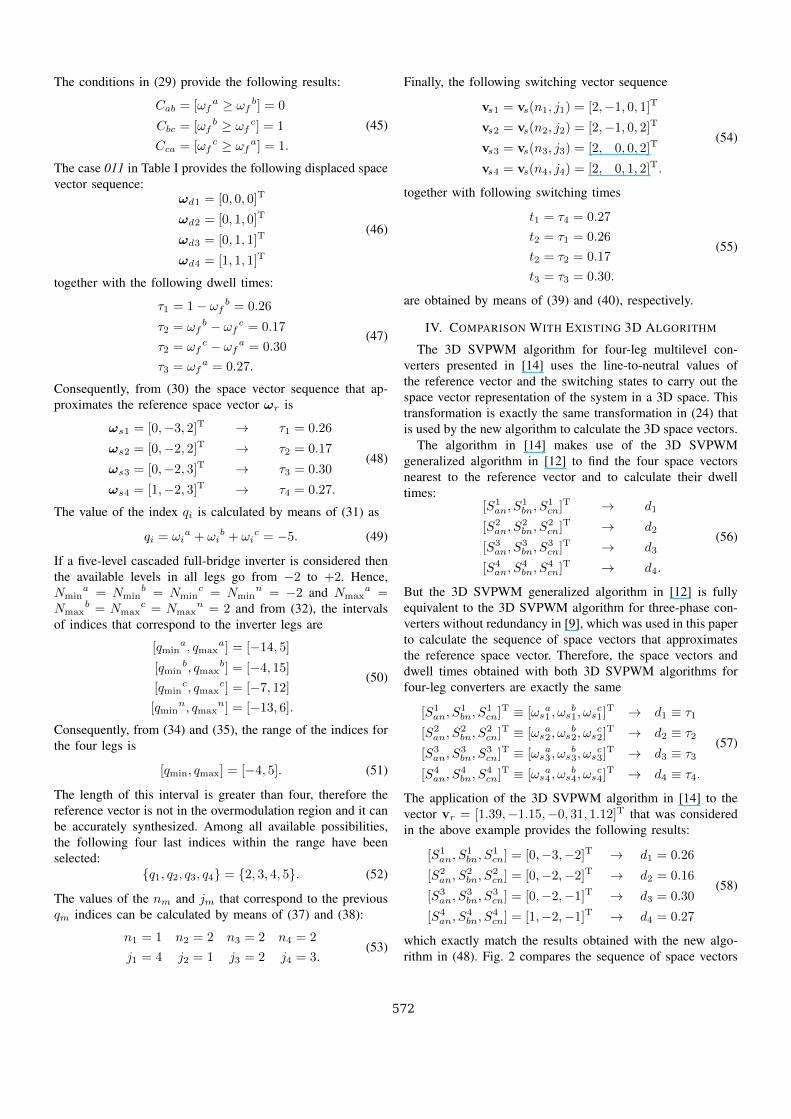
which exactly match the results obtained with the new algo-rithm in (48). Fig. 2 compares the sequence of space vectors
572
0 0.5 1−2
−1
0
1
2V
olta
ge (
p.u.
)Normalized reference voltage
a
b
c
n
0 0.5 1−4
−2
0
2
4
Spa
ce v
ecto
r se
quen
ce
New 3D SVPWM algorithm
Wa WbWc
0 0.5 1−4
−2
0
2
4
Spa
ce v
ecto
r se
quen
ce
Multilevel 3D SVPWM algorithm in [14]
San SbnScn
0 0.5 1−1
−0.5
0
0.5
1
Time (p.u.)
Diff
. (%
)
Difference between both algoritms
Wa-San Wb-Sbn Wc-ScnFig. 2. Comparison of the space vector sequence obtained with both 3DSVPWM algorithms.
{ωsj} obtained with both modulation algorithms showingidentical results, as well.
Consequently, the 3D SVPWM algorithm presented in [14]is fully equivalent to the part of the new 3D SVPWM thatcalculates the space vectors and the dwell times, which wasdescribed in section III-A. The part that carries out theswitching state selection, described in section III-B, is notaddressed in [14]. Therefore, the new modulation algorithmfor four-leg converters can be considered as an extension ofthe algorithm in [14] that solves the switching state selectionproblem.
V. EXPERIMENTAL RESULTS
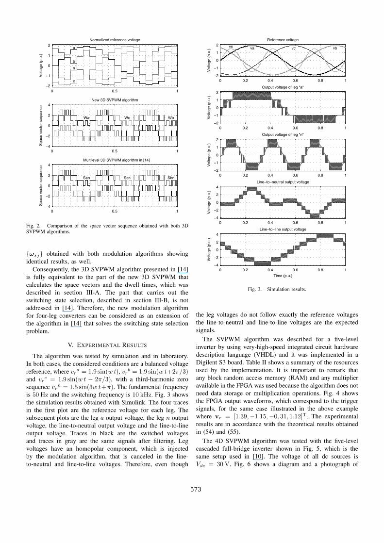
The algorithm was tested by simulation and in laboratory.In both cases, the considered conditions are a balanced voltagereference, where vra = 1.9 sin(w t), vrb = 1.9 sin(w t+2π/3)and vr
c = 1.9 sin(w t − 2π/3), with a third-harmonic zerosequence vrn = 1.5 sin(3w t+π). The fundamental frequencyis 50 Hz and the switching frequency is 10 kHz. Fig. 3 showsthe simulation results obtained with Simulink. The four tracesin the first plot are the reference voltage for each leg. Thesubsequent plots are the leg a output voltage, the leg n outputvoltage, the line-to-neutral output voltage and the line-to-lineoutput voltage. Traces in black are the switched voltagesand traces in gray are the same signals after filtering. Legvoltages have an homopolar component, which is injectedby the modulation algorithm, that is canceled in the line-to-neutral and line-to-line voltages. Therefore, even though
0 0.2 0.4 0.6 0.8 1−2
−1
0
1
2
Vol
tage
(p.
u.)
Reference voltage
va vbvcvn
0 0.2 0.4 0.6 0.8 1−2
−1
0
1
2
Vol
tage
(p.
u.)
Output voltage of leg "a"
0 0.2 0.4 0.6 0.8 1−2
−1
0
1
2
Vol
tage
(p.
u.)
Output voltage of leg "n"
0 0.2 0.4 0.6 0.8 1−4
−2
0
2
4
Vol
tage
(p.
u.)
Line−to−neutral output voltage
0 0.2 0.4 0.6 0.8 1−4
−2
0
2
4
Vol
tage
(p.
u.)
Line−to−line output voltage
Time (p.u.)
Fig. 3. Simulation results.
the leg voltages do not follow exactly the reference voltagesthe line-to-neutral and line-to-line voltages are the expectedsignals.
The SVPWM algorithm was described for a five-levelinverter by using very-high-speed integrated circuit hardwaredescription language (VHDL) and it was implemented in aDigilent S3 board. Table II shows a summary of the resourcesused by the implementation. It is important to remark thatany block random access memory (RAM) and any multiplieravailable in the FPGA was used because the algorithm does notneed data storage or multiplication operations. Fig. 4 showsthe FPGA output waveforms, which correspond to the triggersignals, for the same case illustrated in the above examplewhere vr = [1.39,−1.15,−0, 31, 1.12]T. The experimentalresults are in accordance with the theoretical results obtainedin (54) and (55).
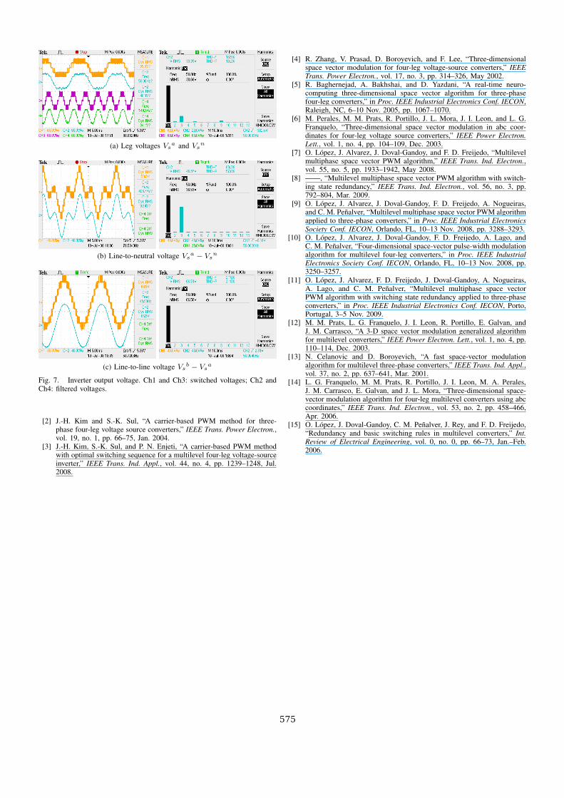
The 4D SVPWM algorithm was tested with the five-levelcascaded full-bridge inverter shown in Fig. 5, which is thesame setup used in [10]. The voltage of all dc sources isVdc = 30 V. Fig. 6 shows a diagram and a photograph of
573
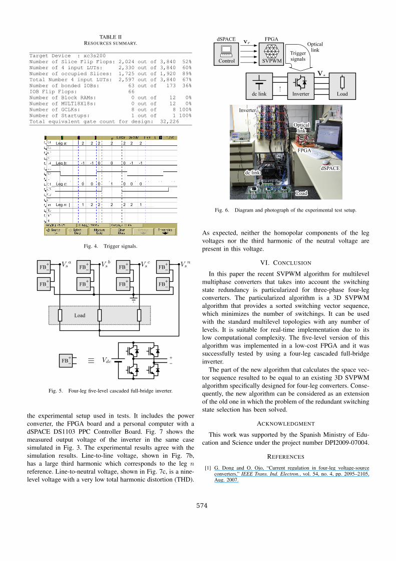
TABLE IIRESOURCES SUMMARY.
Target Device : xc3s200Number of Slice Flip Flops: 2,024 out of 3,840 52%Number of 4 input LUTs: 2,330 out of 3,840 60%Number of occupied Slices: 1,725 out of 1,920 89%Total Number 4 input LUTs: 2,597 out of 3,840 67%Number of bonded IOBs: 63 out of 173 36%IOB Flip Flops: 66Number of Block RAMs: 0 out of 12 0%Number of MULT18X18s: 0 out of 12 0%Number of GCLKs: 8 out of 8 100%Number of Startups: 1 out of 1 100%Total equivalent gate count for design: 32,226
Fig. 4. Trigger signals.
Fig. 5. Four-leg five-level cascaded full-bridge inverter.
the experimental setup used in tests. It includes the powerconverter, the FPGA board and a personal computer with adSPACE DS1103 PPC Controller Board. Fig. 7 shows themeasured output voltage of the inverter in the same casesimulated in Fig. 3. The experimental results agree with thesimulation results. Line-to-line voltage, shown in Fig. 7b,has a large third harmonic which corresponds to the leg nreference. Line-to-neutral voltage, shown in Fig. 7c, is a nine-level voltage with a very low total harmonic distortion (THD).
Fig. 6. Diagram and photograph of the experimental test setup.
As expected, neither the homopolar components of the legvoltages nor the third harmonic of the neutral voltage arepresent in this voltage.
VI. CONCLUSION
In this paper the recent SVPWM algorithm for multilevelmultiphase converters that takes into account the switchingstate redundancy is particularized for three-phase four-legconverters. The particularized algorithm is a 3D SVPWMalgorithm that provides a sorted switching vector sequence,which minimizes the number of switchings. It can be usedwith the standard multilevel topologies with any number oflevels. It is suitable for real-time implementation due to itslow computational complexity. The five-level version of thisalgorithm was implemented in a low-cost FPGA and it wassuccessfully tested by using a four-leg cascaded full-bridgeinverter.
The part of the new algorithm that calculates the space vec-tor sequence resulted to be equal to an existing 3D SVPWMalgorithm specifically designed for four-leg converters. Conse-quently, the new algorithm can be considered as an extensionof the old one in which the problem of the redundant switchingstate selection has been solved.
ACKNOWLEDGMENT
This work was supported by the Spanish Ministry of Edu-cation and Science under the project number DPI2009-07004.
REFERENCES
[1] G. Dong and O. Ojo, “Current regulation in four-leg voltage-sourceconverters,” IEEE Trans. Ind. Electron., vol. 54, no. 4, pp. 2095–2105,Aug. 2007.
574
(a) Leg voltages Vsa and Vsn
(b) Line-to-neutral voltage Vsa − Vsn
(c) Line-to-line voltage Vsb − Vsa
Fig. 7. Inverter output voltage. Ch1 and Ch3: switched voltages; Ch2 andCh4: filtered voltages.
[2] J.-H. Kim and S.-K. Sul, “A carrier-based PWM method for three-phase four-leg voltage source converters,” IEEE Trans. Power Electron.,vol. 19, no. 1, pp. 66–75, Jan. 2004.
[3] J.-H. Kim, S.-K. Sul, and P. N. Enjeti, “A carrier-based PWM methodwith optimal switching sequence for a multilevel four-leg voltage-sourceinverter,” IEEE Trans. Ind. Appl., vol. 44, no. 4, pp. 1239–1248, Jul.2008.
[4] R. Zhang, V. Prasad, D. Boroyevich, and F. Lee, “Three-dimensionalspace vector modulation for four-leg voltage-source converters,” IEEETrans. Power Electron., vol. 17, no. 3, pp. 314–326, May 2002.
[5] R. Baghernejad, A. Bakhshai, and D. Yazdani, “A real-time neuro-computing three-dimensional space vector algorithm for three-phasefour-leg converters,” in Proc. IEEE Industrial Electronics Conf. IECON,Raleigh, NC, 6–10 Nov. 2005, pp. 1067–1070.
[6] M. Perales, M. M. Prats, R. Portillo, J. L. Mora, J. I. Leon, and L. G.Franquelo, “Three-dimensional space vector modulation in abc coor-dinates for four-leg voltage source converters,” IEEE Power Electron.Lett., vol. 1, no. 4, pp. 104–109, Dec. 2003.
[7] O. López, J. Alvarez, J. Doval-Gandoy, and F. D. Freijedo, “Multilevelmultiphase space vector PWM algorithm,” IEEE Trans. Ind. Electron.,vol. 55, no. 5, pp. 1933–1942, May 2008.
[8] ——, “Multilevel multiphase space vector PWM algorithm with switch-ing state redundancy,” IEEE Trans. Ind. Electron., vol. 56, no. 3, pp.792–804, Mar. 2009.
[9] O. López, J. Alvarez, J. Doval-Gandoy, F. D. Freijedo, A. Nogueiras,and C. M. Peñalver, “Multilevel multiphase space vector PWM algorithmapplied to three-phase converters,” in Proc. IEEE Industrial ElectronicsSociety Conf. IECON, Orlando, FL, 10–13 Nov. 2008, pp. 3288–3293.
[10] O. López, J. Alvarez, J. Doval-Gandoy, F. D. Freijedo, A. Lago, andC. M. Peñalver, “Four-dimensional space-vector pulse-width modulationalgorithm for multilevel four-leg converters,” in Proc. IEEE IndustrialElectronics Society Conf. IECON, Orlando, FL, 10–13 Nov. 2008, pp.3250–3257.
[11] O. López, J. Alvarez, F. D. Freijedo, J. Doval-Gandoy, A. Nogueiras,A. Lago, and C. M. Peñalver, “Multilevel multiphase space vectorPWM algorithm with switching state redundancy applied to three-phaseconverters,” in Proc. IEEE Industrial Electronics Conf. IECON, Porto,Portugal, 3–5 Nov. 2009.
[12] M. M. Prats, L. G. Franquelo, J. I. Leon, R. Portillo, E. Galvan, andJ. M. Carrasco, “A 3-D space vector modulation generalized algorithmfor multilevel converters,” IEEE Power Electron. Lett., vol. 1, no. 4, pp.110–114, Dec. 2003.
[13] N. Celanovic and D. Boroyevich, “A fast space-vector modulationalgorithm for multilevel three-phase converters,” IEEE Trans. Ind. Appl.,vol. 37, no. 2, pp. 637–641, Mar. 2001.
[14] L. G. Franquelo, M. M. Prats, R. Portillo, J. I. Leon, M. A. Perales,J. M. Carrasco, E. Galvan, and J. L. Mora, “Three-dimensional space-vector modulation algorithm for four-leg multilevel converters using abccoordinates,” IEEE Trans. Ind. Electron., vol. 53, no. 2, pp. 458–466,Apr. 2006.
[15] O. López, J. Doval-Gandoy, C. M. Peñalver, J. Rey, and F. D. Freijedo,“Redundancy and basic switching rules in multilevel converters,” Int.Review of Electrical Engineering, vol. 0, no. 0, pp. 66–73, Jan.–Feb.2006.
575