LM5020 100V Current Mode PWM Controller
12
LM5020 100V Current Mode PWM Controller General Description The LM5020 high voltage pulse-width-modulation (PWM) controller contains all of the features needed to implement single ended primary power converter topologies. Output voltage regulation is based on current-mode control, which eases the design of loop compensation while providing in- herent line feed-forward. The LM5020 includes a high- voltage start-up regulator that operates over a wide input range up to 100V. The PWM controller is designed for high speed capability including an oscillator frequency range to 1MHz and total propagation delays less than 100ns. Addi- tional features include an error amplifier, precision reference, line under-voltage lockout, cycle-by-cycle current limit, slope compensation, softstart, oscillator synchronization capability and thermal shutdown. The controller is available in both MSOP-10 and LLP-10 packages. Features n Internal Start-up Bias Regulator n Error Amplifier n Precision Voltage Reference n Programmable Softstart n 1A Peak Gate Driver n Maximum Duty Cycle Limiting (80% for LM5020-1 or 50% for LM5020-2) n Programmable Line Under Voltage Lockout (UVLO) with Adjustable Hysteresis n Cycle-by-Cycle Over-Current Protection n Slope Compensation (LM5020-1) n Programmable Oscillator Frequency with Synchronization Capability n Current Sense Leading Edge Blanking n Thermal Shutdown Protection Packages n MSOP-10 n LLP-10 (4 mm x 4 mm) Connection Diagram Top View 20095001 10-Lead MSOP, LLP Ordering Information Order Number Description NSC Package Drawing Supplied As LM5020MM-1 MSOP, 80% Duty Cycle Limit MUB-10A 1000 Units on Tape and Reel LM5020MMX-1 MSOP, 80% Duty Cycle Limit MUB-10A 3500 Units on Tape and Reel LM5020SD-1 LLP, 80% Duty Cycle Limit SDC-10A 1000 Units on Tape and Reel LM5020SDX-1 LLP, 80% Duty Cycle Limit SDC-10A 4500 Units on Tape and Reel LM5020MM-2 MSOP, 50% Duty Cycle Limit MUB-10A 1000 Units on Tape and Reel LM5020MMX-2 MSOP, 50% Duty Cycle Limit MUB-10A 3500 Units on Tape and Reel LM5020SD-2 LLP, 50% Duty Cycle Limit SDC-10A 1000 Units on Tape and Reel LM5020SDX-2 LLP, 50% Duty Cycle Limit SDC-10A 4500 Units on Tape and Reel October 2004 LM5020 100V Current Mode PWM Controller © 2004 National Semiconductor Corporation DS200950 www.national.com 查询LM5020供应商 捷多邦,专业PCB打样工厂,24小时加急出货
-
Upload
khangminh22 -
Category
Documents
-
view
1 -
download
0
Transcript of LM5020 100V Current Mode PWM Controller
LM5020100V Current Mode PWM ControllerGeneral DescriptionThe LM5020 high voltage pulse-width-modulation (PWM)controller contains all of the features needed to implementsingle ended primary power converter topologies. Outputvoltage regulation is based on current-mode control, whicheases the design of loop compensation while providing in-herent line feed-forward. The LM5020 includes a high-voltage start-up regulator that operates over a wide inputrange up to 100V. The PWM controller is designed for highspeed capability including an oscillator frequency range to1MHz and total propagation delays less than 100ns. Addi-tional features include an error amplifier, precision reference,line under-voltage lockout, cycle-by-cycle current limit, slopecompensation, softstart, oscillator synchronization capabilityand thermal shutdown. The controller is available in bothMSOP-10 and LLP-10 packages.
Featuresn Internal Start-up Bias Regulatorn Error Amplifiern Precision Voltage Referencen Programmable Softstartn 1A Peak Gate Drivern Maximum Duty Cycle Limiting (80% for LM5020-1 or
50% for LM5020-2)n Programmable Line Under Voltage Lockout (UVLO) with
Adjustable Hysteresisn Cycle-by-Cycle Over-Current Protectionn Slope Compensation (LM5020-1)n Programmable Oscillator Frequency with
Synchronization Capabilityn Current Sense Leading Edge Blankingn Thermal Shutdown Protection
Packagesn MSOP-10n LLP-10 (4 mm x 4 mm)
Connection Diagram
Top View
20095001
10-Lead MSOP, LLP
Ordering Information
Order Number Description NSC Package Drawing Supplied As
LM5020MM-1 MSOP, 80% Duty Cycle Limit MUB-10A 1000 Units on Tape and Reel
LM5020MMX-1 MSOP, 80% Duty Cycle Limit MUB-10A 3500 Units on Tape and Reel
LM5020SD-1 LLP, 80% Duty Cycle Limit SDC-10A 1000 Units on Tape and Reel
LM5020SDX-1 LLP, 80% Duty Cycle Limit SDC-10A 4500 Units on Tape and Reel
LM5020MM-2 MSOP, 50% Duty Cycle Limit MUB-10A 1000 Units on Tape and Reel
LM5020MMX-2 MSOP, 50% Duty Cycle Limit MUB-10A 3500 Units on Tape and Reel
LM5020SD-2 LLP, 50% Duty Cycle Limit SDC-10A 1000 Units on Tape and Reel
LM5020SDX-2 LLP, 50% Duty Cycle Limit SDC-10A 4500 Units on Tape and Reel
October 2004
LM5020
100VC
urrentM
odeP
WM
Controller
© 2004 National Semiconductor Corporation DS200950 www.national.com
查询LM5020供应商 捷多邦,专业PCB打样工厂,24小时加急出货

Block Diagram
20095002
FIGURE 1.
LM50
20
www.national.com 2
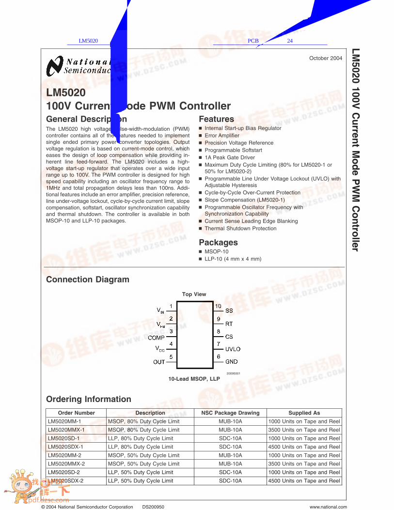
Pin Description
PIN NAME DESCRIPTION APPLICATION INFORMATION
1 Vin Source Input Voltage Input to start-up regulator. Input range13V to 100V.
2 FB Feedback Signal Inverting input of the internal erroramplifier. The non-inverting input isinternally connected to a 1.25Vreference.
3 COMP The output of the erroramplifier and input to thePulse Width Modulator
COMP pull-up is provided by aninternal 5K resistor which may beused to bias an opto-couplertransistor.
4 VCC Output of the internal highvoltage series pass regulator.Regulated output voltage 7.7V
If an auxiliary winding raises thevoltage on this pin above theregulation set point, the internal seriespass regulator will shutdown, reducingthe controller power dissipation.
5 OUT Output of the PWM controller Gate driver output with a 1A peakcurrent capability
6 GND Ground return
7 UVLO Line Under-Voltage Shutdown An external resistor divider from thepower converter source sets theshutdown levels. The threshold ofoperation equals 1.25V. Hysteresis isset by a switched internal 20µAcurrent source.
8 CS Current Sense input Current sense input for current modecontrol and over-current protection.Current limiting is accomplished usinga dedicated current sense comparator.If the CS comparator input exceeds0.5V the OUT pin switches low forcycle-by-cycle current limiting. CS isheld low for 50ns after OUT switcheshigh to blank leading edge currentspikes.
9 RT / SYNC Oscillator timing resistor pinand synchronization input
An external resistor connected fromRT to GND sets the oscillatorfrequency. This pin will also acceptsynchronization pulses from anexternal clock.
10 SS Softstart Input An external capacitor and an internal10µA current source set the soft-startramp rate.
LM5020
www.national.com3

Absolute Maximum Ratings (Note 1)
If Military/Aerospace specified devices are required,please contact the National Semiconductor Sales Office/Distributors for availability and specifications.
VIN to GND -0.3V to 100V
VCC to GND -0.3V to 16V
RT to GND -0.3V to 5.5V
All other pins to GND -0.3V to 7V
Power Dissipation Internally Limited
ESD Rating (Note 2)Human Body Model 2kV
Storage Temperature -55˚C to +150˚C
Junction Temperature 150˚C
Operating RatingsVIN Voltage 13V to 90V
External Voltage applied to VCC 8V to 15V
Operating Junction Temperature -40˚C to +125˚C
Electrical CharacteristicsSpecifications in standard type face are for TJ= +25˚C and those in boldface type apply over the full operating junction tem-perature range. Unless otherwise specified: VIN = 48V, VCC = 10V, and RT = 31.6KΩ
Symbol Parameter Conditions Min Typ Max Units
Startup Regulator
VCCReg VCC Regulation Open ckt 7.4 7.7 8.0 V
VCC Current Limit (Note 4) 15 22 mA
I-VIN Startup Regulator Leakage VIN = 100V 150 500 µA
IIN Shutdown Current VUVLO = 0V, VCC = open 250 350 µA
VCC Supply
VCC UVLO (Rising) VccReg- 300mV
VccReg -100mV
V
VCC UVLO (Falling) 5.3 6.0 6.7 V
ICC Supply Current Cload = 0 2 3 mA
Error Amplifier
GBW Gain Bandwidth 4 MHz
DC Gain 75 dB
Input Voltage VFB = COMP 1.225 1.25 1.275 V
COMP Sink Capability VFB = 1.5V COMP= 1V 5 17 mA
Line UVLO Shutdown
Shutdown Threshold 1.225 1.25 1.275 V
Undervoltage ShutdownHysteresis Current Source
16 20 24 µA
Current Limit
ILIM Delay to Output CS step from 0 to 0.6VTime to onset of OUTTransition (90%)
30 ns
CS Cycle by Cycle CS ThresholdVoltage
0.45 0.5 0.55 V
Leading Edge Blanking Time 50 ns
CS Sink Impedance (clocked) 35 55 ΩSoft Start
Softstart Current Source 7 10 13 µA
Softstart to COMP Offset 0.35 0.55 0.75 V
LM50
20
www.national.com 4
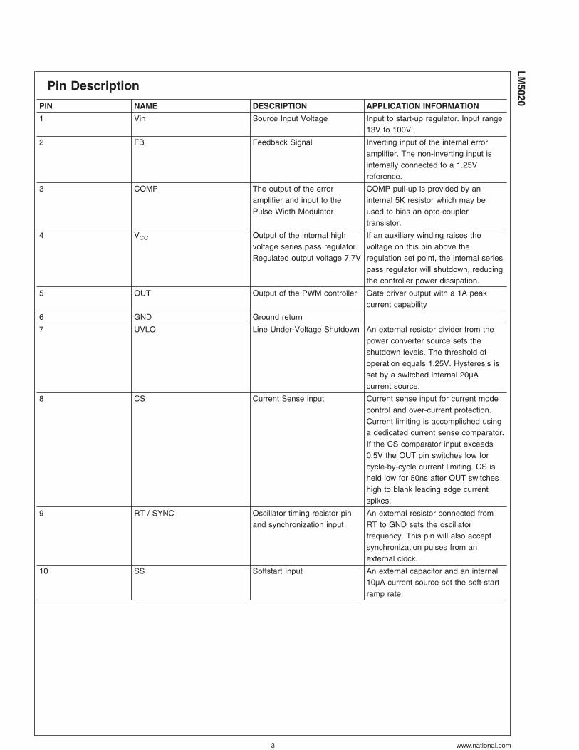
Electrical Characteristics (Continued)
Specifications in standard type face are for TJ= +25˚C and those in boldface type apply over the full operating junction tem-perature range. Unless otherwise specified: VIN = 48V, VCC = 10V, and RT = 31.6KΩ
Symbol Parameter Conditions Min Typ Max Units
Oscillator
Frequency1 (RT = 31.6k) (Note 5) 175 200 225 kHz
Frequency2 (RT = 9.76k) (Note 5) 560 630 700 kHz
Sync threshold 2.4 3.2 3.8 V
PWM Comparator
Delay to Output COMP set to 2V CSstepped 0 to 0.4V, Timeto onset of OUT transitionlow
25 ns
Min Duty Cycle COMP=0V 0 %
Max Duty Cycle (-1 Device) 75 80 85 %
Max Duty Cycle (-2 Device) 50 %
COMP to PWM ComparatorGain
0.33
COMP Open Circuit Voltage 4.3 5.2 6.1 V
COMP Short Circuit Current COMP=0V 0.6 1.1 1.5 mA
Slope Compensation
Slope Comp Amplitude(LM5020-1 Device Only)
Delta increase at PWMComparator to CS
80 105 130 mV
Output Section
Output High Saturation Iout = 50mA, VCC - VOUT 0.25 0.75 V
Output Low Saturation IOUT = 100mA, VOUT 0.25 0.75 V
Rise Time Cload = 1nF 18 ns
Fall Time Cload = 1nF 15 ns
Thermal Shutdown
Tsd Thermal Shutdown Temp. 165 ˚C
Thermal Shutdown Hysteresis 25 ˚C
Note 1: Absolute Maximum Ratings are limits beyond which damage to the device may occur. Operating Ratings are conditions under which operation of the deviceis intended to be functional. For guaranteed specifications and test conditions, see the Electrical Characteristics.
Note 2: The human body model is a 100 pF capacitor discharged through a 1.5kΩ resistor.
Note 3: Limits are 100% production tested at 25˚C. Limits over the operating temperature range are guaranteed through correlation using Statistical Quality Control(SQC) methods. The limits are used to calculate National’s Average Outgoing Quality Level (AOQL).
Note 4: Device thermal limitations may limit usable range.
Note 5: Specification applies to the oscillator frequency. The operational frequency of the LM5020-2 devices is divided by two.
LM5020
www.national.com5
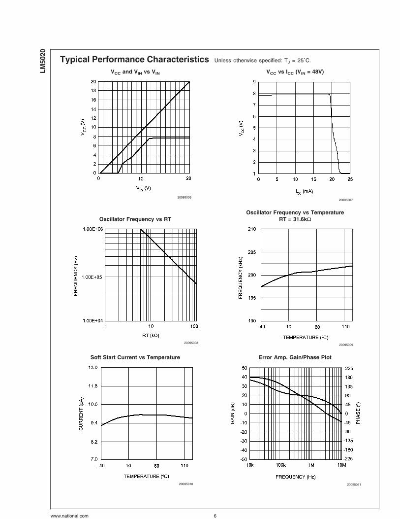
Typical Performance Characteristics Unless otherwise specified: TJ = 25˚C.
VCC and VIN vs VIN VCC vs ICC (VIN = 48V)
2009500620095007
Oscillator Frequency vs RTOscillator Frequency vs Temperature
RT = 31.6kΩ
2009500820095009
Soft Start Current vs Temperature Error Amp. Gain/Phase Plot
20095010 20095021
LM50
20
www.national.com 6
Detailed Operating DescriptionThe LM5020 High Voltage PWM controller contains all of thefeatures needed to implement single ended primary powerconverter topologies. The LM5020 includes a high-voltagestartup regulator that operates over a wide input range to100V. The PWM controller is designed for high speed capa-bility including an oscillator frequency range to 1MHz andtotal propagation delays less than 100ns. Additional featuresinclude an error amplifier, precision reference, line under-voltage lockout, cycle-by-cycle current limit, slope compen-sation, softstart, oscillator sync capability and thermal shut-down. The functional block diagram of the LM5020 is shownin Figure 1. The LM5020 is designed for current-mode con-trol power converters, which require a single drive output,such as Flyback and Forward topologies. The LM5020 pro-vides all of the advantages of current-mode control includingline feed-forward, cycle-by-cycle current limiting and simpli-fied loop compensation .
High Voltage Start-Up RegulatorThe LM5020 contains an internal high voltage startup regu-lator, that allows the input pin (Vin) to be connected directlyto line voltages as high as 100V. The regulator output isinternally current limited to 15mA. When power is applied,the regulator is enabled and sources current into an externalcapacitor connected to the VCC pin. The recommended ca-pacitance range for the Vcc regulator is 0.1µF to 100µF.When the voltage on the VCC pin reaches the regulationlevel of 7.7V, the controller output is enabled. The controllerwill remain enabled until VCC falls below 6V.
In typical applications, a transformer auxiliary winding isconnected through a diode to the VCC pin. This windingshould raise the VCC voltage above 8V to shut off the internalstartup regulator. Powering VCC from an auxiliary windingimproves conversion efficiency while reducing the powerdissipated in the controller. The external VCC capacitor mustbe selected such that the capacitor maintains the Vcc volt-age greater than the VCC UVLO falling threshold (6V) duringthe initial start-up. During a fault condition when the con-verter auxiliary winding is inactive, external current draw onthe VCC line should be limited such that the power dissipatedin the start-up regulator does not exceed the maximumpower dissipation capability of the controller.
An external start-up or other bias rail can be used instead ofthe internal start-up regulator by connecting the VCC and theVin pins together and feeding the external bias voltage (8-15V) to the two pins.
Line Under Voltage DetectorThe LM5020 contains a line Under Voltage Lock Out (UVLO)circuit. An external set-point voltage divider from Vin to GNDsets the operational range of the converter. The resistordivider must be designed such that the voltage at the UVLOpin is greater than 1.25V when Vin is in the desired operatingrange. If the under voltage threshold is not met, all functionsof the controller are disabled and the controller remains in alow power standby state.
UVLO hysteresis is accomplished with an internal 20µAcurrent source that is switched on or off into the impedanceof the set-point divider. When the UVLO threshold is ex-ceeded, the current source is activated to instantly raise thevoltage at the UVLO pin. When the UVLO pin voltage fallsbelow the 1.25V threshold the current source is turned off,causing the voltage at the UVLO pin to fall. The UVLO pincan also be used to implement a remote enable / disablefunction. If an external transistor pulls the UVLO pin belowthe 1.25V threshold, the converter will be disabled.
Error AmplifierAn internal high gain error amplifier is provided within theLM5020. The amplifier’s non-inverting input is internally setto a fixed reference voltage of 1.25V. The inverting input isconnected to the FB pin. In non-isolated applications, thepower converter output is connected to the FB pin via volt-age scaling resistors. Loop compensation components areconnected between the COMP and FB pins. For most iso-lated applications the error amplifier function is implementedon the secondary side of the converter and the internal erroramplifier is not used. The internal error amplifier is config-ured as an open drain output and can be disabled by con-necting the FB pin to ground. An internal 5K pull-up resistorbetween a 5V reference and COMP can be used as thepull-up for an optocoupler in isolated applications.
Current Limit/Current SenseThe LM5020 provides a cycle-by-cycle over current protec-tion function. Current limit is accomplished by an internalcurrent sense comparator. If the voltage at current sensecomparator input exceeds 0.5V, the output will be immedi-ately terminated. A small RC filter, located near the control-ler, is recommended to filter noise from the current sensesignal. The CS input has an internal MOSFET which dis-charges the CS pin capacitance at the conclusion of everycycle. The discharge device remains on an additional 50nsafter the beginning of the new cycle to attenuate the leadingedge spike on the current sense signal.
The LM5020 current sense and PWM comparators are veryfast, and may respond to short duration noise pulses. Layoutconsiderations are critical for the current sense filter andsense resistor. The capacitor associated with the CS filtermust be located very close to the device and connecteddirectly to the pins of the controller (CS and GND). If acurrent sense transformer is used, both leads of the trans-former secondary should be routed to the sense resistor andthe current sense filter network. A sense resistor located inthe source of the primary power MOSFET may be used forcurrent sensing, but a low inductance resistor is required.When designing with a current sense resistor all of the noisesensitive low power ground connections should be con-nected together local to the controller and a single connec-tion should be made to the high current power ground (senseresistor ground point).
LM5020
www.national.com7

Oscillator and Sync CapabilityA single external resistor connected between the RT andGND pins sets the LM5020 oscillator frequency. Internal tothe LM5020–2 device (50% duty cycle limited option) is anoscillator divide by two circuit. This divide by two circuitcreates an exact 50% duty cycle pulse which is used inter-nally to create a precise 50% duty cycle limit function. Be-cause of this, the internal oscillator actually operates at twicethe frequency of the output (OUT). For the LM5020–1 devicethe oscillator frequency and the operational output frequencyare the same. To set a desired output operational frequency(F), the RT resistor can be calculated from:
LM5020-1:
LM5020-2:
The LM5020 can also be synchronized to an external clock.The external clock must have a higher frequency than thefree running oscillator frequency set by the RT resistor. Theclock signal should be capacitively coupled into the RT pinwith a 100pF capacitor. A peak voltage level greater than 3.7Volts at the RT pin is required for detection of the sync pulse.The sync pulse width should be set between 15 to 150ns bythe external components. The RT resistor is always required,whether the oscillator is free running or externally synchro-nized. The voltage at the RT pin is internally regulated to a 2Volts. The RT resistor should be located very close to thedevice and connected directly to the pins of the controller(RT and GND).
PWM Comparator / SlopeCompensationThe PWM comparator compares the current ramp signalwith the loop error voltage derived from the error amplifieroutput. The error amplifier output voltage at the COMP pin isoffset by 1.4V and then further attenuated by a 3:1 resistordivider. The PWM comparator polarity is such that 0 Volts onthe COMP pin will result in a zero duty cycle at the controlleroutput. For duty cycles greater than 50 percent, currentmode control circuits are subject to sub-harmonic oscillation.By adding an additional fixed slope voltage ramp signal
(slope compensation) to the current sense signal, this oscil-lation can be avoided. The LM5020-1 integrates this slopecompensation by summing a current ramp generated by theoscillator with the current sense signal. Additional slopecompensation may be added by increasing the source im-pedance of the current sense signal. Since the LM5020-2 isnot capable of duty cycles greater than 50%, there is noslope compensation feature in this device.
Soft StartThe softstart feature allows the power converter to graduallyreach the initial steady state operating point, thereby reduc-ing start-up stresses and current surges. At power on, afterthe VCC and the line undervoltage lockout thresholds aresatisfied, an internal 10µA current source charges an exter-nal capacitor connected to the SS pin. The capacitor voltagewill ramp up slowly and will limit the COMP pin voltage andthe duty cycle of the output pulses.
Gate Driver and Maximum DutyCycle LimitThe LM5020 provides an internal gate driver (OUT), whichcan source and sink a peak current of 1 Amp. The LM5020 isavailable in two duty cycle limit options. The maximum out-put duty cycle is typically 80% for the LM5020-1 option andprecisely equal to 50% for the LM5020-2 option. The maxi-mum duty cycle function for the LM5020-2 is accomplishedwith an internal toggle flip-flop which ensures an accurateduty cycle limit. The internal oscillator frequency of theLM5020-2 is therefore twice the operating frequency of thePWM controller (OUT pin).
The 80% maximum duty cycle limit of the LM5020-1 isdetermined by the internal oscillator and varies more thanthe 50% limit of the LM5020-2. For the LM5020-1 the internaloscillator frequency and the operational frequency of thePWM controller are equal.
Thermal ProtectionInternal thermal shutdown circuitry is provided to protect theintegrated circuit in the event the maximum junction tem-perature is exceeded. This feature prevents catastrophicfailures from accidental device overheating. When activated,typically at 165 degrees Celsius, the controller is forced intoa low power standby state, disabling the output driver andthe bias regulator. After the temperature is reduced (typicalhysteresis = 25˚C) the VCC regulator will be enabled and asoftstart sequence initiated.
LM50
20
www.national.com 8

Typ
ical
Ap
plic
atio
nC
ircu
it:
36V
-75
VIN
and
3.3V
,4.
5AO
UT
2009
5005
LM5020
www.national.com9
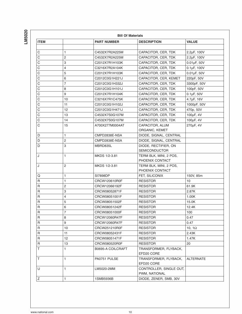
Bill Of Materials
ITEM PART NUMBER DESCRIPTION VALUE
C 1 C4532X7R2A225M CAPACITOR, CER, TDK 2.2µF, 100V
C 2 C4532X7R2A225M CAPACITOR, CER, TDK 2.2µF, 100V
C 3 C2012X7R1H103K CAPACITOR, CER, TDK 0.01µF, 50V
C 4 C3216X7R2A104K CAPACITOR, CER, TDK 0.1µF, 100V
C 5 C2012X7R1H103K CAPACITOR, CER, TDK 0.01µF, 50V
C 6 C2012C0G1H221J CAPACITOR, CER, KEMET 220pF, 50V
C 7 C2012C0G1H332J CAPACITOR, CER, TDK 3300pF, 50V
C 8 C2012C0G1H101J CAPACITOR, CER, TDK 100pF, 50V
C 9 C2012X7R1H104K CAPACITOR, CER, TDK 0.1µF, 50V
C 10 C3216X7R1C475K CAPACITOR, CER, TDK 4.7µF, 16V
C 11 C2012C0G1H102J CAPACITOR, CER, TDK 1000pF, 50V
C 12 C2012C0G1H471J CAPACITOR, CER, TDK 470p, 50V
C 13 C4532X7S0G107M CAPACITOR, CER, TDK 100µF, 4V
C 14 C4532X7S0G107M CAPACITOR, CER, TDK 100µF, 4V
C 15 A700X277M0004AT CAPACITOR, ALUMORGANIC, KEMET
270µF, 4V
D 1 CMPD2838E-NSA DIODE, SIGNAL, CENTRAL
D 2 CMPD2838E-NSA DIODE, SIGNAL, CENTRAL
D 3 MBRD835L DIODE, RECTIFIER, ONSEMICONDUCTOR
J 1 MKDS 1/2-3.81 TERM BLK, MINI, 2 POS,PHOENIX CONTACT
J 2 MKDS 1/2-3.81 TERM BLK, MINI, 2 POS,PHOENIX CONTACT
Q 1 SI7898DP FET, SILICONIX 150V, 85m
R 1 CRCW120610R0F RESISTOR 10
R 2 CRCW12066192F RESISTOR 61.9K
R 3 CRCW08052871F RESISTOR 2.87K
R 4 CRCW08051001F RESISTOR 1.00K
R 5 CRCW08051502F RESISTOR 15.0K
R 6 CRCW08051242F RESISTOR 12.4K
R 7 CRCW08051000F RESISTOR 100
R 8 CRCW12060R47F RESISTOR 0.47
R 9 CRCW12060R47F RESISTOR 0.47
R 10 CRCW251210R0F RESISTOR 10, 1ΩR 11 CRCW08052431F RESISTOR 2.43K
R 12 CRCW08051471F RESISTOR 1.47K
R 13 CRCW080520R0F RESISTOR 20
T 1 B0695-A COILCRAFT TRANSFORMER, FLYBACK,EFD20 CORE
T 1 PA0751 PULSE TRANSFORMER, FLYBACK,EFD20 CORE
ALTERNATE
U 1 LM5020-2MM CONTROLLER, SINGLE OUT,PWM, NATIONAL
Z 1 1SMB5936B DIODE, ZENER, SMB, 30V
LM50
20
www.national.com 10

Physical Dimensions inches (millimeters)unless otherwise noted
10 Lead MSOP PackageNS Package Number MUB10A
10 Lead MSOP, LLP PackageNS Package Number SDC10A
LM5020
www.national.com11

Notes
National does not assume any responsibility for use of any circuitry described, no circuit patent licenses are implied and National reservesthe right at any time without notice to change said circuitry and specifications.
For the most current product information visit us at www.national.com.
LIFE SUPPORT POLICY
NATIONAL’S PRODUCTS ARE NOT AUTHORIZED FOR USE AS CRITICAL COMPONENTS IN LIFE SUPPORT DEVICES OR SYSTEMSWITHOUT THE EXPRESS WRITTEN APPROVAL OF THE PRESIDENT AND GENERAL COUNSEL OF NATIONAL SEMICONDUCTORCORPORATION. As used herein:
1. Life support devices or systems are devices or systemswhich, (a) are intended for surgical implant into the body, or(b) support or sustain life, and whose failure to perform whenproperly used in accordance with instructions for useprovided in the labeling, can be reasonably expected to resultin a significant injury to the user.
2. A critical component is any component of a life supportdevice or system whose failure to perform can be reasonablyexpected to cause the failure of the life support device orsystem, or to affect its safety or effectiveness.
BANNED SUBSTANCE COMPLIANCE
National Semiconductor certifies that the products and packing materials meet the provisions of the Customer Products StewardshipSpecification (CSP-9-111C2) and the Banned Substances and Materials of Interest Specification (CSP-9-111S2) and contain no ‘‘BannedSubstances’’ as defined in CSP-9-111S2.
National SemiconductorAmericas CustomerSupport CenterEmail: [email protected]: 1-800-272-9959
National SemiconductorEurope Customer Support Center
Fax: +49 (0) 180-530 85 86Email: [email protected]
Deutsch Tel: +49 (0) 69 9508 6208English Tel: +44 (0) 870 24 0 2171Français Tel: +33 (0) 1 41 91 8790
National SemiconductorAsia Pacific CustomerSupport CenterEmail: [email protected]
National SemiconductorJapan Customer Support CenterFax: 81-3-5639-7507Email: [email protected]: 81-3-5639-7560
www.national.com
LM50
2010
0VC
urre
ntM
ode
PW
MC
ontr
olle
r


![kkt_6_dan_7_pemupukan_2014 [Compatibility Mode]](https://static.fdokumen.com/doc/165x107/6322b43c28c445989105e2db/kkt6dan7pemupukan2014-compatibility-mode.jpg)