MAX8553/MAX8554 4.5V to 28V Input, Synchronous PWM ...
24
General Description The MAX8553 is a 4.5V to 28V input-voltage, synchro- nous step-down controller that provides a complete power-management solution for DDR memory. The MAX8553 generates 1/2 V REFIN voltage for VTT and VTTR. The VTT and VTTR tracking voltages are main- tained within 1% of 1/2 V REFIN . The MAX8554 is a 4.5V to 28V input voltage, nontracking step-down controller with a low 0.6V feedback threshold voltage. The MAX8553/ MAX8554 use Maxim’s proprietary Quick-PWM™ archi- tecture for fast transient response and operate with selectable pseudo-fixed frequencies. Both controllers can operate without an external bias supply. The controllers operate in synchronous-rectification mode to ensure balanced current sourcing and sinking capabili- ty of up to 25A. The MAX8553/MAX8554 also provide up to 95% efficiency, making them ideal for server and point- of-load applications. Additionally, a low 5μA shutdown current allows for longer battery life in notebook applica- tions. Lossless current monitoring is achieved by monitor- ing the low-side MOSFET’s drain-to-source voltage. The MAX8553/MAX8554 have an adjustable foldback current limit to withstand a continuous output overload and short circuit. Digital soft-start provides control of inrush current during power-up. Overvoltage protection shuts the con- verter down and discharges the output capacitor. The MAX8553/MAX8554 come in space-saving 16-pin QSOP packages. Applications Wide-Input Power Supplies Servers and Storage Applications ASIC and CPU Core Voltages Notebook and LCD-PC Power Supplies DDR I and DDR II Memory Power Supplies AGTL Bus Termination Supplies Features ♦ Up to 25A Output-Current Capability ♦ Quick-PWM Control for Fast Loop Response ♦ Up to 95% Efficiency ♦ 4.5V to 28V Input Voltage Range ♦ No External Bias Supply Required ♦ 0 to 3.6V Input REFIN Range (MAX8553) ♦ Automatically Sets VTT and VTTR to within ±1% of 1/2 V REFIN - (MAX8553) ♦ Low 0.6V Feedback Threshold (MAX8554) ♦ 200kHz/300kHz/400kHz/550kHz Selectable Switching Frequencies ♦ Adjustable Foldback Current Limit ♦ Overvoltage Protection ♦ Digital Soft-Start MAX8553/MAX8554 4.5V to 28V Input, Synchronous PWM Buck Controllers for DDR Termination and Point-of-Load Applications ________________________________________________________________ Maxim Integrated Products 1 Ordering Information MAX8553 DH EN/HSD +5V POK VIN VOUT VTTR V+ REFIN LX DL VTTR GND POK REFIN VL BST V+ REF ILIM FSEL PGND VTT PART TEMP RANGE PIN-PACKAGE MAX8553EEE -40°C to +85°C 16 QSOP MAX8554EEE -40°C to +85°C 16 QSOP Typical Operating Circuit 19-3017; Rev 1; 5/05 For pricing, delivery, and ordering information, please contact Maxim/Dallas Direct! at 1-888-629-4642, or visit Maxim’s website at www.maxim-ic.com. Pin Configurations appear at end of data sheet. Quick-PWM is a trademark of Maxim Integrated Products, Inc.
-
Upload
khangminh22 -
Category
Documents
-
view
1 -
download
0
Transcript of MAX8553/MAX8554 4.5V to 28V Input, Synchronous PWM ...

General DescriptionThe MAX8553 is a 4.5V to 28V input-voltage, synchro-nous step-down controller that provides a completepower-management solution for DDR memory. TheMAX8553 generates 1/2 VREFIN voltage for VTT andVTTR. The VTT and VTTR tracking voltages are main-tained within 1% of 1/2 VREFIN. The MAX8554 is a 4.5V to28V input voltage, nontracking step-down controller witha low 0.6V feedback threshold voltage. The MAX8553/MAX8554 use Maxim’s proprietary Quick-PWM™ archi-tecture for fast transient response and operate withselectable pseudo-fixed frequencies. Both controllerscan operate without an external bias supply.
The controllers operate in synchronous-rectification modeto ensure balanced current sourcing and sinking capabili-ty of up to 25A. The MAX8553/MAX8554 also provide upto 95% efficiency, making them ideal for server and point-of-load applications. Additionally, a low 5µA shutdowncurrent allows for longer battery life in notebook applica-tions. Lossless current monitoring is achieved by monitor-ing the low-side MOSFET’s drain-to-source voltage. TheMAX8553/MAX8554 have an adjustable foldback currentlimit to withstand a continuous output overload and shortcircuit. Digital soft-start provides control of inrush currentduring power-up. Overvoltage protection shuts the con-verter down and discharges the output capacitor. TheMAX8553/MAX8554 come in space-saving 16-pin QSOPpackages.
ApplicationsWide-Input Power Supplies
Servers and Storage Applications
ASIC and CPU Core Voltages
Notebook and LCD-PC Power Supplies
DDR I and DDR II Memory Power Supplies
AGTL Bus Termination Supplies
Features♦ Up to 25A Output-Current Capability
♦ Quick-PWM Control for Fast Loop Response
♦ Up to 95% Efficiency
♦ 4.5V to 28V Input Voltage Range
♦ No External Bias Supply Required
♦ 0 to 3.6V Input REFIN Range (MAX8553)
♦ Automatically Sets VTT and VTTR to within ±1%of 1/2 VREFIN- (MAX8553)
♦ Low 0.6V Feedback Threshold (MAX8554)
♦ 200kHz/300kHz/400kHz/550kHz SelectableSwitching Frequencies
♦ Adjustable Foldback Current Limit
♦ Overvoltage Protection
♦ Digital Soft-Start
MA
X8
55
3/M
AX
85
54
4.5V to 28V Input, Synchronous PWM Buck Controllersfor DDR Termination and Point-of-Load Applications
________________________________________________________________ Maxim Integrated Products 1
Ordering Information
MAX8553
DHEN/HSD
+5V
POK
VIN
VOUT
VTTR
V+
REFIN
LX
DL
VTTRGND
POK
REFIN
VL
BST
V+
REF
ILIM
FSEL
PGND
VTTPART TEMP RANGE PIN-PACKAGE
MAX8553EEE -40°C to +85°C 16 QSOP
MAX8554EEE -40°C to +85°C 16 QSOP
Typical Operating Circuit
19-3017; Rev 1; 5/05
For pricing, delivery, and ordering information, please contact Maxim/Dallas Direct! at 1-888-629-4642, or visit Maxim’s website at www.maxim-ic.com.
Pin Configurations appear at end of data sheet.
Quick-PWM is a trademark of Maxim Integrated Products, Inc.
MA
X8
55
3/M
AX
85
54
4.5V to 28V Input, Synchronous PWM Buck Controllersfor DDR Termination and Point-of-Load Applications
2 _______________________________________________________________________________________
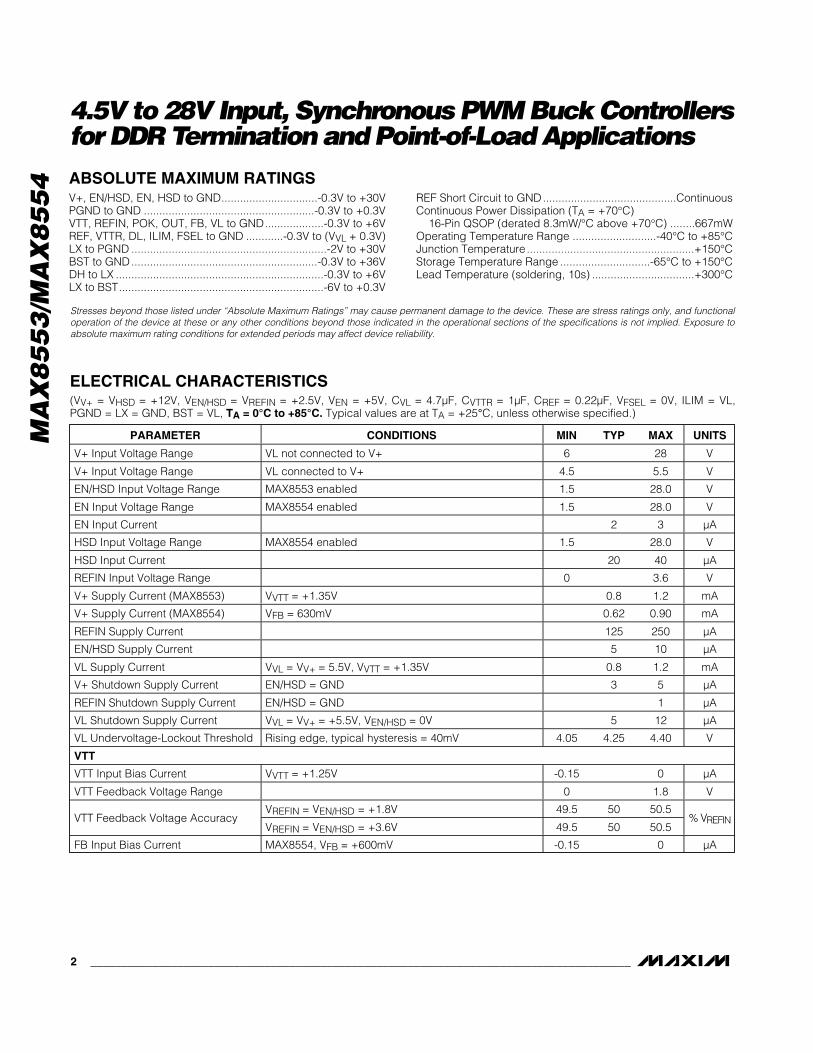
ABSOLUTE MAXIMUM RATINGS
ELECTRICAL CHARACTERISTICS(VV+ = VHSD = +12V, VEN/HSD = VREFIN = +2.5V, VEN = +5V, CVL = 4.7µF, CVTTR = 1µF, CREF = 0.22µF, VFSEL = 0V, ILIM = VL,PGND = LX = GND, BST = VL, TA = 0°C to +85°C. Typical values are at TA = +25°C, unless otherwise specified.)
Stresses beyond those listed under “Absolute Maximum Ratings” may cause permanent damage to the device. These are stress ratings only, and functionaloperation of the device at these or any other conditions beyond those indicated in the operational sections of the specifications is not implied. Exposure toabsolute maximum rating conditions for extended periods may affect device reliability.
V+, EN/HSD, EN, HSD to GND...............................-0.3V to +30VPGND to GND .......................................................-0.3V to +0.3VVTT, REFIN, POK, OUT, FB, VL to GND...................-0.3V to +6VREF, VTTR, DL, ILIM, FSEL to GND ............-0.3V to (VVL + 0.3V)LX to PGND ...............................................................-2V to +30VBST to GND............................................................-0.3V to +36VDH to LX ...................................................................-0.3V to +6VLX to BST..................................................................-6V to +0.3V
REF Short Circuit to GND...........................................ContinuousContinuous Power Dissipation (TA = +70°C)
16-Pin QSOP (derated 8.3mW/°C above +70°C) ........667mWOperating Temperature Range ...........................-40°C to +85°CJunction Temperature ......................................................+150°CStorage Temperature Range .............................-65°C to +150°CLead Temperature (soldering, 10s) .................................+300°C
PARAMETER CONDITIONS MIN TYP MAX UNITS
V+ Input Voltage Range VL not connected to V+ 6 28 V
V+ Input Voltage Range VL connected to V+ 4.5 5.5 V
EN/HSD Input Voltage Range MAX8553 enabled 1.5 28.0 V
EN Input Voltage Range MAX8554 enabled 1.5 28.0 V
EN Input Current 2 3 µA
HSD Input Voltage Range MAX8554 enabled 1.5 28.0 V
HSD Input Current 20 40 µA
REFIN Input Voltage Range 0 3.6 V
V+ Supply Current (MAX8553) VVTT = +1.35V 0.8 1.2 mA
V+ Supply Current (MAX8554) VFB = 630mV 0.62 0.90 mA
REFIN Supply Current 125 250 µA
EN/HSD Supply Current 5 10 µA
VL Supply Current VVL = VV+ = 5.5V, VVTT = +1.35V 0.8 1.2 mA
V+ Shutdown Supply Current EN/HSD = GND 3 5 µA
REFIN Shutdown Supply Current EN/HSD = GND 1 µA
VL Shutdown Supply Current VVL = VV+ = +5.5V, VEN/HSD = 0V 5 12 µA
VL Undervoltage-Lockout Threshold Rising edge, typical hysteresis = 40mV 4.05 4.25 4.40 V
VTT
VTT Input Bias Current VVTT = +1.25V -0.15 0 µA
VTT Feedback Voltage Range 0 1.8 V
VREFIN = VEN/HSD = +1.8V 49.5 50 50.5VTT Feedback Voltage Accuracy
VREFIN = VEN/HSD = +3.6V 49.5 50 50.5% VRE FIN
FB Input Bias Current MAX8554, VFB = +600mV -0.15 0 µA

MA
X8
55
3/M
AX
85
54
4.5V to 28V Input, Synchronous PWM Buck Controllersfor DDR Termination and Point-of-Load Applications
_______________________________________________________________________________________ 3
ELECTRICAL CHARACTERISTICS (continued)(VV+ = VHSD = +12V, VEN/HSD = VREFIN = +2.5V, VEN = +5V, CVL = 4.7µF, CVTTR = 1µF, CREF = 0.22µF, VFSEL = 0V, ILIM = VL,PGND = LX = GND, BST = VL, TA = 0°C to +85°C. Typical values are at TA = +25°C, unless otherwise specified.)
PARAMETER CONDITIONS MIN TYP MAX UNITS
FB Regulation Voltage MAX8554, VOUT = +2.5V, FSEL unconnected 0.598 0.607 0.616 V
Output Adjust Range MAX8554 (Note 1) 0.6 3.5 V
VTT Line Regulation VEN/HSD ±10%, VVTT = +1.25V, IOUT = 0A ±0.325 %
FB Line RegulationMAX8554, VHSD ±10%, VOUT = +2.5V,IOUT = 0A, FSEL unconnected
±0.325 %
VTT Load Regulation 0 < IOUT < +7A, VVTT = +1.25V 0.2 %
FB Load RegulationMAX8554, 0 < IOUT < +7A, VOUT = +2.5V,FSEL unconnected
0.2 %
REFERENCE
Reference Output Voltage VV+ = VVL = +4.5 to +5.5V, IREF = 0 1.97 2.00 2.03 V
Reference Load Regulation VV+ = VVL = +5V, IREF = 0 to 50µA 10 mV
Reference UVLO VV+ = VVL = +5V, reference rising, hysteresis = 27mV 1.5 1.6 1.7 V
VTTR
VTTR Output Voltage Range 0 1.8 VIVTTR = -5mA to +5mA 49.5 50 50.5
IVTTR = -25mA to +25mA, VREFIN = +1.8V 49 50 51VTTR Output Accuracy
IVTTR = -25mA to +25mA, VREFIN = +3.6V 49.5 50 50.5
% VRE FIN
Thermal Shutdown Rising temperature, typical hysteresis = 15°C +160 °C
SOFT-START
ILIM Ramp Period Ramps the ILIM trip threshold from 20% to 100% in20% increments
0.8 1.7 3.0 ms
Output Predischarge Period Rising edge of EN/HSD to the start of internal digitalsoft-start
0.8 1.7 3.0 ms
OSCILLATOR
FSEL = VL 200 FSEL = unconnected 300 FSEL = REF 400 Oscillator Frequency
FSEL = GND 550
kHz
FSEL = VL 2.18 2.5 2.83
FSEL unconnected 1.45 1.67 1.89
FSEL = REF 1.09 1.25 1.41 On-Time
MAX8553, VVTT = +1.25V(Note 2)
FSEL = GND 0.82 0.91 1.00
µs
FSEL = VL 0.89 1.02 1.16
FSEL unconnected 0.61 0.71 0.80
FSEL = REF 0.43 0.49 0.56 On-Time
MAX8554, VOUT = +2.5V(Note 2)
FSEL = GND 0.33 0.37 0.41
µs
Off-Time (Note 2) 350 400 ns
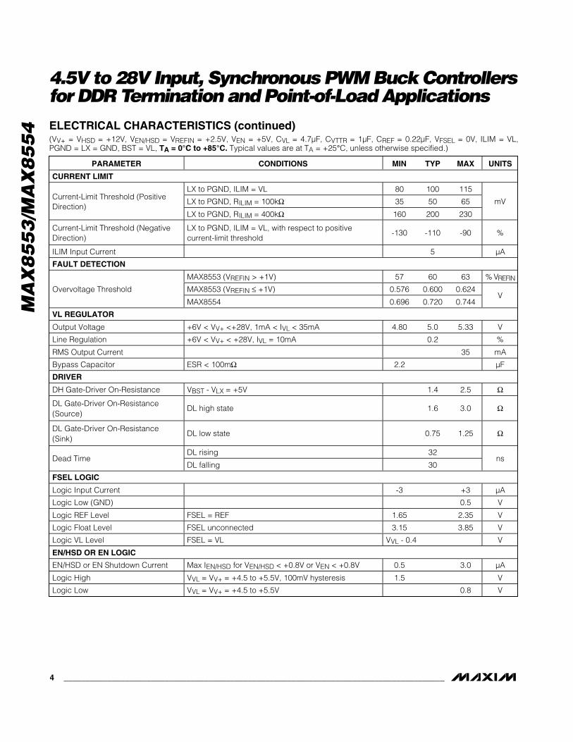
MA
X8
55
3/M
AX
85
54
4.5V to 28V Input, Synchronous PWM Buck Controllersfor DDR Termination and Point-of-Load Applications
4 _______________________________________________________________________________________
ELECTRICAL CHARACTERISTICS (continued)(VV+ = VHSD = +12V, VEN/HSD = VREFIN = +2.5V, VEN = +5V, CVL = 4.7µF, CVTTR = 1µF, CREF = 0.22µF, VFSEL = 0V, ILIM = VL,PGND = LX = GND, BST = VL, TA = 0°C to +85°C. Typical values are at TA = +25°C, unless otherwise specified.)
PARAMETER CONDITIONS MIN TYP MAX UNITS
CURRENT LIMIT
LX to PGND, ILIM = VL 80 100 115
LX to PGND, RILIM = 100kΩ 35 50 65Current-Limit Threshold (PositiveDirection)
LX to PGND, RILIM = 400kΩ 160 200 230
mV
Current-Limit Threshold (NegativeDirection)
LX to PGND, ILIM = VL, with respect to positivecurrent-limit threshold
-130 -110 -90 %
ILIM Input Current 5 µA
FAULT DETECTION
MAX8553 (VREFIN > +1V) 57 60 63 % VRE FIN
MAX8553 (VREFIN ≤ +1V) 0.576 0.600 0.624Overvoltage Threshold
MAX8554 0.696 0.720 0.744V
VL REGULATOR
Output Voltage +6V < VV+ <+28V, 1mA < IVL < 35mA 4.80 5.0 5.33 V Line Regulation +6V < VV+ < +28V, IVL = 10mA 0.2 % RMS Output Current 35 mA
Bypass Capacitor ESR < 100mΩ 2.2 µF
DRIVER
DH Gate-Driver On-Resistance VBST - VLX = +5V 1.4 2.5 Ω
DL Gate-Driver On-Resistance(Source)
DL high state 1.6 3.0 Ω
DL Gate-Driver On-Resistance(Sink)
DL low state 0.75 1.25 Ω
DL rising 32Dead Time
DL falling 30ns
FSEL LOGIC
Logic Input Current -3 +3 µA
Logic Low (GND) 0.5 V
Logic REF Level FSEL = REF 1.65 2.35 V
Logic Float Level FSEL unconnected 3.15 3.85 V
Logic VL Level FSEL = VL VVL - 0.4 V
EN/HSD OR EN LOGIC
EN/HSD or EN Shutdown Current Max IEN/HSD for VEN/HSD < +0.8V or VEN < +0.8V 0.5 3.0 µA
Logic High VVL = VV+ = +4.5 to +5.5V, 100mV hysteresis 1.5 V
Logic Low VVL = VV+ = +4.5 to +5.5V 0.8 V
MA
X8
55
3/M
AX
85
54
4.5V to 28V Input, Synchronous PWM Buck Controllersfor DDR Termination and Point-of-Load Applications
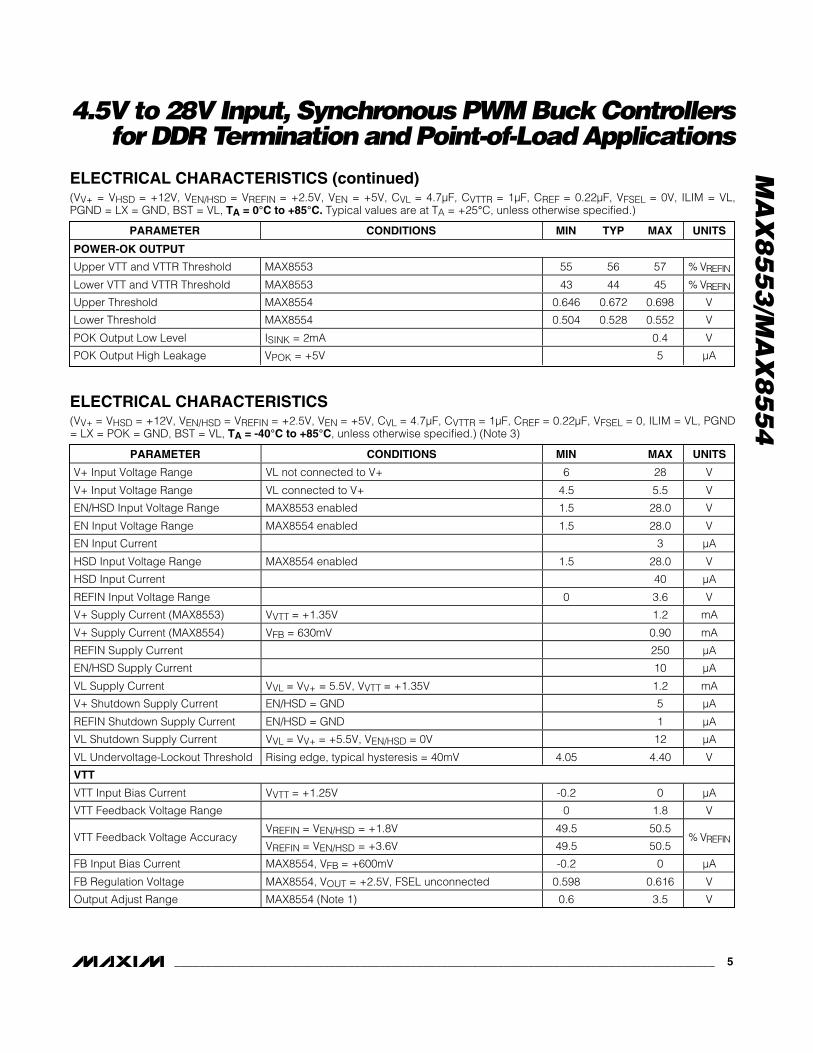
_______________________________________________________________________________________ 5
ELECTRICAL CHARACTERISTICS (continued)(VV+ = VHSD = +12V, VEN/HSD = VREFIN = +2.5V, VEN = +5V, CVL = 4.7µF, CVTTR = 1µF, CREF = 0.22µF, VFSEL = 0V, ILIM = VL,PGND = LX = GND, BST = VL, TA = 0°C to +85°C. Typical values are at TA = +25°C, unless otherwise specified.)
PARAMETER CONDITIONS MIN TYP MAX UNITS
POWER-OK OUTPUT
Upper VTT and VTTR Threshold MAX8553 55 56 57 % VRE FIN
Lower VTT and VTTR Threshold MAX8553 43 44 45 % VRE FIN
Upper Threshold MAX8554 0.646 0.672 0.698 V
Lower Threshold MAX8554 0.504 0.528 0.552 V
POK Output Low Level ISINK = 2mA 0.4 V
POK Output High Leakage VPOK = +5V 5 µA
ELECTRICAL CHARACTERISTICS (VV+ = VHSD = +12V, VEN/HSD = VREFIN = +2.5V, VEN = +5V, CVL = 4.7µF, CVTTR = 1µF, CREF = 0.22µF, VFSEL = 0, ILIM = VL, PGND= LX = POK = GND, BST = VL, TA = -40°C to +85°C, unless otherwise specified.) (Note 3)
PARAMETER CONDITIONS MIN MAX UNITS
V+ Input Voltage Range VL not connected to V+ 6 28 V
V+ Input Voltage Range VL connected to V+ 4.5 5.5 V
EN/HSD Input Voltage Range MAX8553 enabled 1.5 28.0 V
EN Input Voltage Range MAX8554 enabled 1.5 28.0 V
EN Input Current 3 µA
HSD Input Voltage Range MAX8554 enabled 1.5 28.0 V
HSD Input Current 40 µA
REFIN Input Voltage Range 0 3.6 V
V+ Supply Current (MAX8553) VVTT = +1.35V 1.2 mA
V+ Supply Current (MAX8554) VFB = 630mV 0.90 mA
REFIN Supply Current 250 µA
EN/HSD Supply Current 10 µA
VL Supply Current VVL = VV+ = 5.5V, VVTT = +1.35V 1.2 mA
V+ Shutdown Supply Current EN/HSD = GND 5 µA
REFIN Shutdown Supply Current EN/HSD = GND 1 µA
VL Shutdown Supply Current VVL = VV+ = +5.5V, VEN/HSD = 0V 12 µA
VL Undervoltage-Lockout Threshold Rising edge, typical hysteresis = 40mV 4.05 4.40 V
VTT
VTT Input Bias Current VVTT = +1.25V -0.2 0 µA
VTT Feedback Voltage Range 0 1.8 V
VREFIN = VEN/HSD = +1.8V 49.5 50.5VTT Feedback Voltage Accuracy
VREFIN = VEN/HSD = +3.6V 49.5 50.5% VRE FIN
FB Input Bias Current MAX8554, VFB = +600mV -0.2 0 µA
FB Regulation Voltage MAX8554, VOUT = +2.5V, FSEL unconnected 0.598 0.616 V
Output Adjust Range MAX8554 (Note 1) 0.6 3.5 V

MA
X8
55
3/M
AX
85
54
4.5V to 28V Input, Synchronous PWM Buck Controllersfor DDR Termination and Point-of-Load Applications
6 _______________________________________________________________________________________
ELECTRICAL CHARACTERISTICS (continued)(VV+ = VHSD = +12V, VEN/HSD = VREFIN = +2.5V, VEN = +5V, CVL = 4.7µF, CVTTR = 1µF, CREF = 0.22µF, VFSEL = 0, ILIM = VL, PGND= LX = POK = GND, BST = VL, TA = -40°C to +85°C, unless otherwise specified.) (Note 3)
PARAMETER CONDITIONS MIN MAX UNITS
REFERENCE
Reference Output Voltage VV+ = VVL = +4.5 to +5.5V, IREF = 0 1.97 2.03 V
Reference Load Regulation VV+ = VVL = +5V, IREF = 0 to 50µA 10 mV
Reference UVLO VV+ = VVL = +5V, reference rising, hysteresis = 27mV 1.5 1.7 V
VTTR
VTTR Output Voltage Range 0 1.8 V
IVTTR = -5mA to +5mA 49.5 50.5
IVTTR = -25mA to +25mA, VREFIN = +1.8V 49 51VTTR Output Accuracy
IVTTR = -25mA to +25mA, VREFIN = +3.6V 49.5 50.5
% VRE FIN
SOFT-START
ILIM Ramp Period Ramps the ILIM trip threshold from 20% to 100% in20% increments
0.8 3.0 ms
Output Predischarge Period Rising edge of EN/HSD to the start of internal digitalsoft-start
0.8 3.0 ms
OSCILLATOR FSEL = VL 2.18 2.83
FSEL unconnected 1.45 1.89
FSEL = REF 1.09 1.41 On-Time
MAX8553, VVTT = +1.25V(Note 2)
FSEL = GND 0.82 1.00
µs
FSEL = VL 0.89 1.16
FSEL unconnected 0.61 0.80
FSEL = REF 0.43 0.56 On-Time
MAX8554, VOUT = +2.5V(Note 2)
FSEL = GND 0.33 0.41
µs
Off-Time (Note 2) 420 ns
CURRENT LIMIT
LX to PGND, ILIM = VL 80 115
LX to PGND, RILIM = 100kΩ 30 65Current-Limit Threshold (PositiveDirection)
LX to PGND, RILIM = 400kΩ 150 230
mV
Current-Limit Threshold (NegativeDirection)
LX to PGND, ILIM = VL, with respect to positivecurrent-limit threshold
-130 -90 %
ILIM Input Current µA
FAULT DETECTION
MAX8553 (VREFIN > +1V) 57 63 %
MAX8553 (VREFIN ≤ +1V) 0.576 0.624Overvoltage Threshold
MAX8554 0.696 0.744V
VL REGULATOR Output Voltage +6V < VV+ < +28V, 1mA < IVL < 35mA 4.80 5.33 V RMS Output Current 35 mA
Bypass Capacitor ESR < 100mΩ 2.2 µF
MA
X8
55
3/M
AX
85
54
4.5V to 28V Input, Synchronous PWM Buck Controllersfor DDR Termination and Point-of-Load Applications
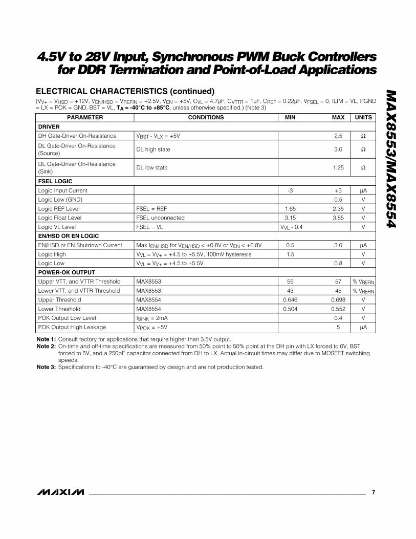
_______________________________________________________________________________________ 7
ELECTRICAL CHARACTERISTICS (continued)(VV+ = VHSD = +12V, VEN/HSD = VREFIN = +2.5V, VEN = +5V, CVL = 4.7µF, CVTTR = 1µF, CREF = 0.22µF, VFSEL = 0, ILIM = VL, PGND= LX = POK = GND, BST = VL, TA = -40°C to +85°C, unless otherwise specified.) (Note 3)
PARAMETER CONDITIONS MIN MAX UNITS
DRIVER
DH Gate-Driver On-Resistance VBST - VLX = +5V 2.5 Ω
DL Gate-Driver On-Resistance(Source)
DL high state 3.0 Ω
DL Gate-Driver On-Resistance(Sink)
DL low state 1.25 Ω
FSEL LOGIC
Logic Input Current -3 +3 µA
Logic Low (GND) 0.5 V
Logic REF Level FSEL = REF 1.65 2.35 V
Logic Float Level FSEL unconnected 3.15 3.85 V
Logic VL Level FSEL = VL VVL - 0.4 V
EN/HSD OR EN LOGIC
EN/HSD or EN Shutdown Current Max IEN/HSD for VEN/HSD < +0.8V or VEN < +0.8V 0.5 3.0 µA
Logic High VVL = VV+ = +4.5 to +5.5V, 100mV hysteresis 1.5 V
Logic Low VVL = VV+ = +4.5 to +5.5V 0.8 V
POWER-OK OUTPUT
Upper VTT, and VTTR Threshold MAX8553 55 57 % VRE FIN
Lower VTT, and VTTR Threshold MAX8553 43 45 % VRE FIN
Upper Threshold MAX8554 0.646 0.698 V
Lower Threshold MAX8554 0.504 0.552 V
POK Output Low Level ISINK = 2mA 0.4 V
POK Output High Leakage VPOK = +5V 5 µA
Note 1: Consult factory for applications that require higher than 3.5V output.Note 2: On-time and off-time specifications are measured from 50% point to 50% point at the DH pin with LX forced to 0V, BST
forced to 5V, and a 250pF capacitor connected from DH to LX. Actual in-circuit times may differ due to MOSFET switchingspeeds.
Note 3: Specifications to -40°C are guaranteed by design and are not production tested.
1.19
1.23
1.21
1.27
1.25
1.29
1.31
0 42 6 8
LOAD REGULATION(CIRCUIT OF FIGURE 2)
MAX
8553
/4 to
c09
LOAD CURRENT (A)
OUTP
UT V
OLTA
GE (V
)
VTT CONNECTED ASSHOWN IN FIGURE 2
VTT CONNECTEDTO THE OUTPUT
MA
X8
55
3/M
AX
85
54
4.5V to 28V Input, Synchronous PWM Buck Controllersfor DDR Termination and Point-of-Load Applications
8 _______________________________________________________________________________________
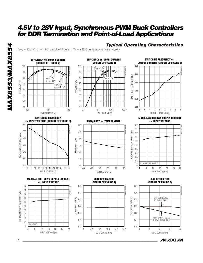
Typical Operating Characteristics(VV+ = 12V, VOUT = 1.8V, circuit of Figure 1, TA = +25°C, unless otherwise noted.)
100
300.1 1.0 10.0
EFFICIENCY vs. LOAD CURRENT(CIRCUIT OF FIGURE 2)
60
MAX
8553
/4 to
c01
LOAD CURRENT (A)
EFFI
CIEN
CY (%
)
70
40
50
80
90
VIN = 1.8VVOUT = 0.9V
VIN = 2.5VVOUT = 1.25V
0.1 10.0 100.0
EFFICIENCY vs. LOAD CURRENT(CIRCUIT OF FIGURE 1)
MAX
8553
/4 to
c02
LOAD CURRENT (A)
EFFI
CIEN
CY (%
)
1.0
100
30
40
50
60
70
90
80 VOUT = 1.8V
VOUT = 2.5V
400
450
550
500
600
650
-8 -4 -2-6 0 2 4 6 8
SWITCHING FREQUENCY vs.OUTPUT CURRENT (CIRCUIT OF FIGURE 2)
MAX
8553
/4 to
c03
OUTPUT CURRENT (A)
SWIT
CHIN
G FR
EQUE
NCY
(kHz
)
200
240
220
280
260
300
320
6 8 10 12 14 16 18 20 22 24 26 28
SWITCHING FREQUENCYvs. INPUT VOLTAGE (CIRCUIT OF FIGURE 3)
MAX
8553
/4 to
c04
INPUT VOLTAGE (V)
SWIT
CHIN
G FR
EQUE
NCY
(kHz
)
160
180
170
200
190
210
220
-40 -15 10 35 60 85
FREQUENCY vs. TEMPERATUREM
AX85
53/4
toc0
5
TEMPERATURE (°C)
FREQ
UENC
Y (k
Hz)
0
4.0
3.5
3.0
2.5
2.0
1.5
1.0
0.5
4.5
5.0
4 8 12 16 20 24 28
MAX8554 SHUTDOWN SUPPLY CURRENTvs. INPUT VOLTAGE
MAX
8553
/4 to
c06
INPUT VOLTAGE (V)
SHUT
DOW
N SU
PPLY
CUR
RENT
(µA)
V+ = HSD, EN = GND
0
4.0
3.5
3.0
2.5
2.0
1.5
1.0
0.5
4.5
5.0
4 8 12 16 20 24 28
MAX8553 SHUTDOWN SUPPLY CURRENTvs. INPUT VOLTAGE
MAX
8553
/4 to
c07
INPUT VOLTAGE (V)
SHUT
DOW
N SU
PPLY
CUR
RENT
(µA)
EN = GND1.74
1.78
1.76
1.82
1.80
1.84
1.86
0 4.0 8.0 12.0 16.0 20.0
LOAD REGULATION(CIRCUIT OF FIGURE 1)
MAX
8553
/4 to
c08
LOAD CURRENT (A)
OUTP
UT V
OLTA
GE (V
)
MA
X8
55
3/M
AX
85
54
4.5V to 28V Input, Synchronous PWM Buck Controllersfor DDR Termination and Point-of-Load Applications
_______________________________________________________________________________________ 9
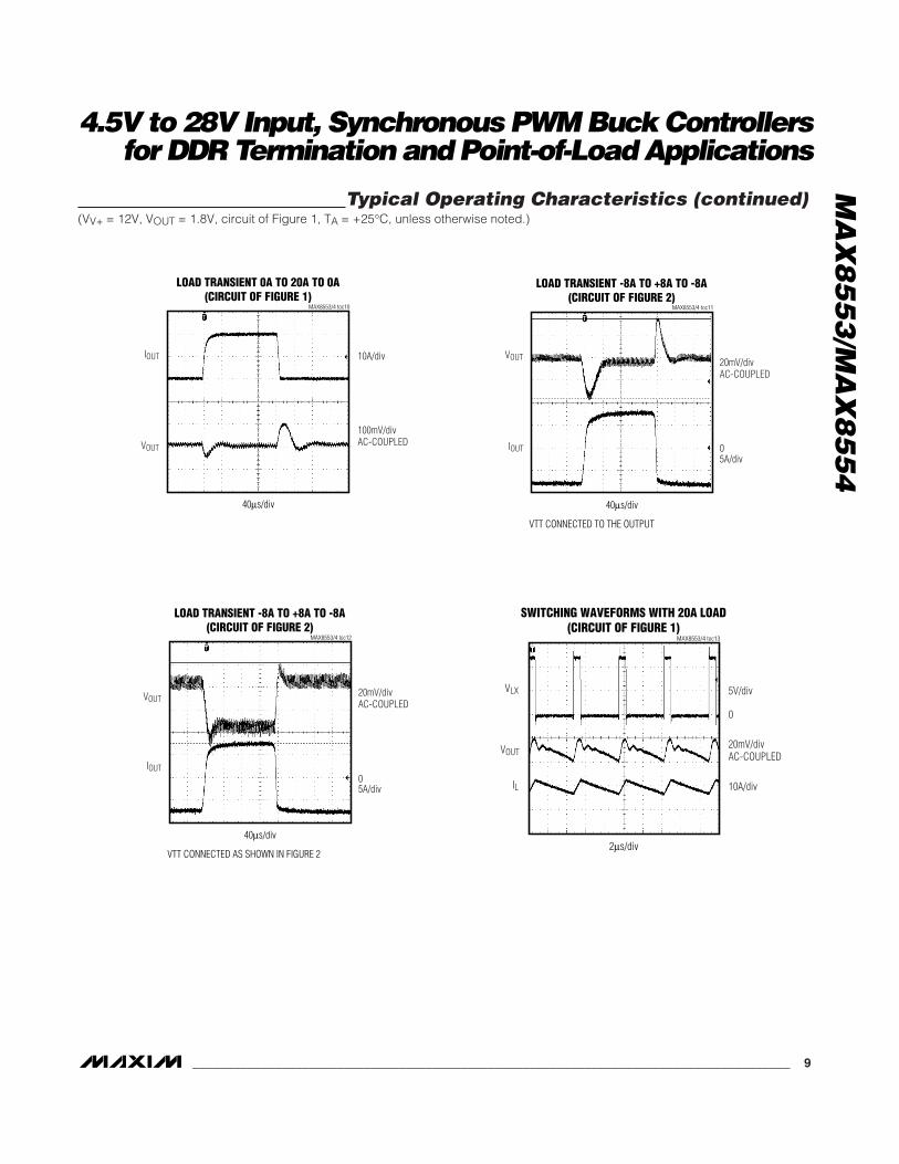
Typical Operating Characteristics (continued)(VV+ = 12V, VOUT = 1.8V, circuit of Figure 1, TA = +25°C, unless otherwise noted.)
LOAD TRANSIENT 0A TO 20A TO 0A(CIRCUIT OF FIGURE 1)
MAX8553/4 toc10
40µs/div
IOUT 10A/div
100mV/divAC-COUPLEDVOUT
LOAD TRANSIENT -8A TO +8A TO -8A(CIRCUIT OF FIGURE 2)
MAX8553/4 toc11
40µs/div
VTT CONNECTED TO THE OUTPUT
VOUT
05A/div
20mV/divAC-COUPLED
IOUT
LOAD TRANSIENT -8A TO +8A TO -8A(CIRCUIT OF FIGURE 2)
MAX8553/4 toc12
40µs/div
VTT CONNECTED AS SHOWN IN FIGURE 2
VOUT
05A/div
20mV/divAC-COUPLED
IOUT
SWITCHING WAVEFORMS WITH 20A LOAD(CIRCUIT OF FIGURE 1)
MAX8553/4 toc13
2µs/div
VLX
IL 10A/div
0
5V/div
20mV/divAC-COUPLED
VOUT
MA
X8
55
3/M
AX
85
54
4.5V to 28V Input, Synchronous PWM Buck Controllersfor DDR Termination and Point-of-Load Applications
10 ______________________________________________________________________________________
Typical Operating Characteristics (continued)(VV+ = 12V, VOUT = 1.8V, circuit of Figure 1, TA = +25°C, unless otherwise noted.)
POWER-UP WAVEFORMS WITH 20A LOAD(CIRCUIT OF FIGURE 1)
MAX8553/4 toc14
2ms/div
VIN
IL 10A/div
10V/div
0
1V/div
5V/divVPOK
VOUT
POWER-DOWN WAVEFORMS WITH 20A LOAD(CIRCUIT OF FIGURE 1)
MAX8553/4 toc15
1ms/div
VIN
IL 10A/div
10V/div
0
1V/div
5V/divVPOK
VOUT
STARTUP/SHUTDOWN WAVEFORMS WITH20A LOAD (CIRCUIT OF FIGURE 1)
MAX8553/4 toc16
2ms/div
VEN
IIN2A/div
5V/div
0
1V/div
5V/divVPOK
VOUT
SHORT CIRCUIT AND RECOVERY(CIRCUIT OF FIGURE 1)
MAX8553/4 toc17
200µs/div
VLX
IL
20V/div
5A/div
1V/div
0V
0A
VOUT

MA
X8
55
3/M
AX
85
54
4.5V to 28V Input, Synchronous PWM Buck Controllersfor DDR Termination and Point-of-Load Applications
______________________________________________________________________________________ 11
Pin Description
PIN MAX8553 MAX8554 FUNCTION
EN/HSD —Enable/High-Side Drain. Connect to the high-side N-channel MOSFET drain through a 5.1kΩresistor for normal operation. Connect to GND for low-power shutdown (Figure 2). If the enablefunction is not used, connect EN/HSD directly to the high-side N-channel MOSFET drain.1
— HSD High-Side Drain. Connect to the high-side N-channel MOSFET drain for normal operation.
REFIN —Reference Input. An applied voltage at REFIN sets VVTT and VVTTR to 1/2 VREFIN. REFIN voltagerange is from 0 to +3.6V.
2
— ENEnable. Drive EN high to enable the output. Drive EN low to shut down the IC. If the enablefunction is not used, connect EN to V+.
3 POK POKPower-OK Output. POK is an open-drain output and is logic high when both VTT and VTTR arewithin 12% of regulation. POK is pulled low in shutdown.
VTT — VTT Feedback Input. Connect to VTT output.
4— FB
Output Feedback. Connect to the center of a resistor-divider between the output and ground toset the output voltage. FB threshold is 0.6V.
5 ILIM ILIMCurrent-Limit Threshold Adjustment. Connect a resistor from ILIM to GND to set the current-limitthreshold, or connect ILIM to VL for the default setting. See the Setting the Current Limit section.
6 FSEL FSELFrequency Select. Selects the switching frequency. See Tables 1 and 2 for configuration ofFSEL.
7 REF REF Reference. Connect a 0.22µF or greater capacitor from REF to GND.
8 GND GND Ground
VTTR —VTTR Reference Output. Connect a 1µF or greater capacitor from VTTR to GND. VTTR iscapable of sourcing and sinking up to 25mA.
9
— OUTOutput Voltage. Connect directly to the output. OUT senses the output voltage to determine theon-time for the high-side switching MOSFET.
10 V+ V+Input Supply Voltage. Supply input for the VL regulator. Bypass with a 0.22µF or greatercapacitor.
11 VL VLInternal Regulator Output. Connect a 2.2µF or greater capacitor from VL to GND. VL can beconnected to V+ if the operating range is from +4.5V to +5.5V.
12 DL DLLow-Side MOSFET Gate Drive. Connect to the gate of the low-side N-channel MOSFET. DL islow in shutdown or in undervoltage lockout.
13 PGND PGND Power Ground
14 BST BSTBootstrapped Supply. Drives high-side N-channel MOSFET. Connect a 0.1µF or greatercapacitor from BST to LX.
15 DH DHHigh-Side MOSFET Gate Drive. Connect to the high-side N-channel MOSFET gate. DH is low inshutdown or in undervoltage lockout.
16 LX LX Inductor Switching Node

Functional Diagrams
Σ
Σ
Q
S
R
Q TRIG
ONE-SHOT
TRIG Q
ONE-SHOT
TON
ON-TIMECOMPUTE
VTT
LATCH
Q
R S
VTTR
VTTPOK
ERRORCOMP
OVP
60%
56%50%
44%
VL
0.6V
5VREG
2VREF
/10
5µA
MAX8553
FSEL
POK
REFIN
EN/HSD
VTTR
GND
REF
VL
VTT
PGND
DL
V+
LX
DH
BST
ILIM
MA
X8
55
3/M
AX
85
54
4.5V to 28V Input, Synchronous PWM Buck Controllersfor DDR Termination and Point-of-Load Applications
12 ______________________________________________________________________________________

MA
X8
55
3/M
AX
85
54
4.5V to 28V Input, Synchronous PWM Buck Controllersfor DDR Termination and Point-of-Load Applications
______________________________________________________________________________________ 13
Functional Diagrams (continued)
Σ
Σ
Q
S
R
Q TRIG
ONE-SHOT
TRIG Q
ONE-SHOT
TON
ON-TIMECOMPUTE
OUT
LATCH
Q
R S
FB
POK
ERRORCOMP
OVP
VL
5VREG
2VREF
/10
5µA
MAX8554
FSEL
POK
GND
REF
VL
FB
PGND
DL
V+
LX
DH
BST
ILIM
EN
HSD
0.672V
0.528V
0.720V
0.600V
MA
X8
55
3/M
AX
85
54
4.5V to 28V Input, Synchronous PWM Buck Controllersfor DDR Termination and Point-of-Load Applications
14 ______________________________________________________________________________________
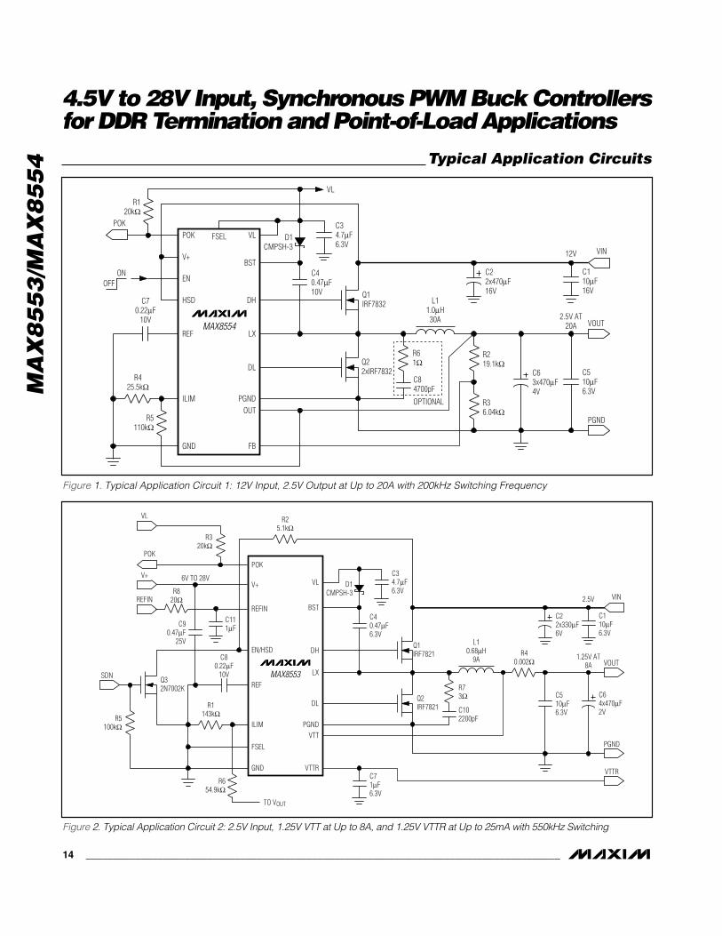
Typical Application Circuits
C40.47µF10V Q1
IRF7832
Q22xIRF7832
L11.0µH30A
R61Ω
C84700pF
OPTIONAL
R219.1kΩ
R36.04kΩ
C63x470µF4V
C510µF6.3V
VOUT
PGND
C34.7µF6.3V
D1CMPSH-3
2.5V AT20A
12V VIN
C22x470µF16V
C110µF16V
MAX8554
VL
POK
R120kΩ
ONOFF
C70.22µF
10V
R425.5kΩ
R5110kΩ
POK
V+
EN
HSD
REF
ILIM
GND
FSEL VL
BST
DH
LX
DL
PGNDOUT
FB
Figure 1. Typical Application Circuit 1: 12V Input, 2.5V Output at Up to 20A with 200kHz Switching Frequency
C40.47µF6.3V
Q1IRF7821
Q2IRF7821
L10.68µH
9A
C510µF6.3V
C64x470µF2V
VOUT
PGND
C34.7µF6.3V
D1CMPSH-3
1.25V AT8A
2.5V VIN
C22x330µF6V
C110µF6.3V
MAX8553
POK
R320kΩ
C80.22µF
10V
6V TO 28V
R1143kΩ
R654.9kΩ
POK
V+
REFIN
EN/HSD
REF
ILIM
GND
FSEL
VL
BST
DH
LX
DL
PGNDVTT
VTTR VTTRC71µF6.3V
VL
V+
REFIN
C90.47µF
25V
SDN
R5100kΩ
Q32N7002K
TO VOUT
R25.1kΩ
R40.002Ω
C102200pF
R73Ω
R820Ω
C111µF
Figure 2. Typical Application Circuit 2: 2.5V Input, 1.25V VTT at Up to 8A, and 1.25V VTTR at Up to 25mA with 550kHz Switching

MA
X8
55
3/M
AX
85
54
4.5V to 28V Input, Synchronous PWM Buck Controllersfor DDR Termination and Point-of-Load Applications
______________________________________________________________________________________ 15
Detailed DescriptionInternal Linear Regulator
An internal regulator produces the +5V supply (VL) thatpowers the PWM controller, MOSFET driver, logic, refer-ence, and other blocks within the IC. This +5V low-dropout (LDO) linear regulator supplies up to 35mA forMOSFET gate-drive and external loads. For supply volt-ages between +4.5V and +5.5V, connect VL to V+. Thisbypasses the VL regulator, which improves efficiencyand allows the IC to function at lower input voltages.
On-Time One-Shot and Switching Frequency
The heart of the PWM is the one-shot that sets the high-side switch on-time. This fast, low-jitter, adjustable one-shot includes circuitry that varies the on-time inresponse to both input and output voltages. The high-side switch on-time is inversely proportional to the inputvoltage as measured by the EN/HSD (HSD for theMAX8554) input, and is directly proportional to the out-put voltage. This algorithm results in a nearly constantswitching frequency despite the lack of a fixed-fre-quency clock generator. The switching frequency canbe selected to avoid noise-sensitive regions such as
the 455kHz IF band. Also, with a constant switching fre-quency, the inductor ripple-current operating pointremains relatively constant, resulting in easy designmethodology and predictable output voltage ripple.The general formula for the MAX8553 on-time (tON) is:
where VEN/HSD and VOUT are the voltages measured atEN/HSD and the output, respectively, and K = 1.7µs.The value of N depends on the configuration of FSELand is listed in Table 1.
For the MAX8554, the general formula for on-time (tON) is:
where VHSD and VOUT are the voltages measured atHSD and the output, respectively, and K = 1.7µs. Thevalue of N depends on the configuration of FSEL and islisted in Table 2.
t K N
VVON
HSDOUT = × × ×1
t K N
VVON
EN HSDOUT
/= × × ×1
C40.47µF10V Q1
IRF7807V
Q2IRF7821
L12.5µH10A
R63Ω
C82200pF
R212.1kΩ
R36.04kΩ
C62x470µF4V
C510µF6.3V
VOUT
PGND
C34.7µF6.3V
D1CMPSH-3
1.8V AT8A
17V TO 21V VIN
C2470µF16V
C110µF16V
MAX8554
VL
POK
R120kΩ
ONOFF
C70.22µF
10V
R461.9kΩ
R580.6kΩ
POK
V+
EN
HSD
REF
ILIM
GND
FSEL VL
BST
DH
LX
DL
PGNDOUT
FB
Figure 3. Typical Application Circuit 3: 19V Input, 1.8V Output at Up to 8A with 300kHz Switching Frequency
This algorithm results in a nearly constant switching fre-quency despite the lack of a fixed-frequency clockgenerator. The actual switching frequency, which isgiven by the following equation, varies slightly due tothe voltage drop across the on-resistance of theMOSFETs and the DC resistance of the output inductor:
where D is the duty cycle:
where IO is the output current, RDSONL is the on-resis-tance of the low-side MOSFET, RDSONH is the on-resis-tance of the high-side MOSFET, and RDC is the DCresistance of the output inductor. The ideal switching fre-quency for VREFIN = 2.5V is about 550kHz. Switching fre-quency increases for positive (sourcing) load currentand decreases for negative (sinking) load current, due tothe changing voltage drop across the low-side MOSFET,which changes the inductor-current discharge ramprate. The on-times guaranteed in the ElectricalCharacteristics are also influenced by switching delayscaused by the loading effect of the external powerMOSFETs.
The switching frequency can also be adjusted to avalue other than the preset frequencies by adding aresistor voltage-divider at HSD. See the Adjusting theSwitching Frequency section.
VTTR Reference (MAX8553 Only)The MAX8553’s VTTR output is capable of sourcing orsinking up to 25mA of current. The VTTR output voltageis one-half of the voltage applied to REFIN. BypassVTTR with at least a 1µF ceramic capacitor.
Voltage ReferenceThe voltage at REF is nominally 2.00V. Connect a 0.22µFceramic bypass capacitor between REF and GND.
EN and HSD (MAX8554 Only)EN is a logic input used to enable or shut down theMAX8554. Drive EN high or connect to V+ to enable theoutput. Drive EN low to place the MAX8554 in low-power shutdown mode, reducing input current to lessthan 5µA (typ).
HSD senses the input voltage at the drain of the high-sideMOSFET, which is used to set the high-side MOSFET on-time. For normal operation, connect HSD to the drain ofthe high-side MOSFET.
EN/HSD Function (MAX8553 Only)In order to reduce pin count and package size, theMAX8553 features a dual-function input pin, EN/HSD.When EN/HSD is pulled to ground, the internal circuitrypowers off, reducing current consumption to less than5µA (typ). To enable normal operation, connectEN/HSD to the drain of the high-side MOSFET througha 5.1kΩ resistor (Figure 2). In this configuration, EN/HSDbecomes an input that monitors the high-side MOSFETdrain voltage (converter input voltage) and uses thatmeasurement to calculate the appropriate on-time for theconverter. If the enable function is not used, connectEN/HSD directly to the high-side MOSFET drain.
D
V I R R
V I R ROUT O DSONL DC
HSD O DSONL DSONH
=
+ +( )+ ( )-
f
Dt K NSON
= ≅×1
MA
X8
55
3/M
AX
85
54
4.5V to 28V Input, Synchronous PWM Buck Controllersfor DDR Termination and Point-of-Load Applications
16 ______________________________________________________________________________________
Table 1. Configuration of FSEL (MAX8553)
FSEL CONNECTED TO N tON (µs) FREQUENCY (kHz) CONDITION
Ground 1.07 0.91 550 VOUT / VEN/HSD = 0.5
REF 1.33 1.15 400 VOUT / VEN/HSD = 0.5
Floating 2.00 1.70 300 VOUT / VEN/HSD = 0.5
VL 3.00 2.55 200 VOUT / VEN/HSD = 0.5
Table 2. Configuration of FSEL (MAX8554)
FSEL CONNECTED TO N tON (µs) FREQUENCY (kHz) CONDITION
Ground 1.07 0.37 550 VHSD = 12V, VOUT = 2.5V
REF 1.33 0.49 400 VHSD = 12V, VOUT = 2.5V
Floating 2.00 0.71 300 VHSD = 12V, VOUT = 2.5V
VL 3.00 1.02 200 VHSD = 12V, VOUT = 2.5V
MA
X8
55
3/M
AX
85
54
4.5V to 28V Input, Synchronous PWM Buck Controllersfor DDR Termination and Point-of-Load Applications
______________________________________________________________________________________ 17
Predischarge ModeThe MAX8553/MAX8554 discharge the output to GNDbefore the digital soft-start begins. When EN/HSD (EN)is pulled high, the MAX8553 (MAX8554) starts an inter-nal counter, and forces VDL to VVL. This discharges theoutput to GND through the low-side MOSFET. If the out-put voltage is above ground before enable, the outputvoltage goes slightly negative due to energy stored inthe output LC. If the load cannot tolerate a negative volt-age, place a power Schottky diode from the output toPGND (anode to PGND) to act as a reverse-polarityclamp. The period for this discharge mode is 1.7ms.Both the buck controller and the VTTR buffer are turnedoff during this period. After the predischarge period,both the buck controller and the VTTR buffer are turnedon and go through soft-start.
Digital Soft-StartThe digital soft-start allows a gradual increase of theinternal current-limit level during startup to reduce theinput surge current. The MAX8553/MAX8554 divide thesoft-start period into five phases. During the first phase,the controller limits the current limit to only 20% of thefull current limit. If the output does not reach the regula-tion within 425µs, soft-start enters the second phaseand the current limit is increased by another 20%. Thisprocess repeats until the maximum current limit isreached (after 1.7ms) or when the output reaches thenominal regulation voltage, whichever occurs first.Adding a capacitor in parallel with the external ILIMresistor creates a continuously adjustable analog soft-start function. If the foldback current-limiting feature isimplemented in the application circuit, the maximumcurrent limit is also a function of the output voltage andthe resistors connected to ILIM.
Power-Good Output (POK)POK is the open-drain output of the internal windowcomparators that continuously monitor VTT and VTTRfor the MAX8553 and FB for the MAX8554. POK isactively held low in shutdown, and becomes highimpedance when the outputs are within 12% of theirrespective nominal regulation voltage.
Overvoltage Protection (OVP)When the buck output voltage rises above 120% of thenominal regulation voltage, the OVP circuit sets thefault latch, shuts down the PWM controller, and immedi-ately pulls DH low and forces DL high. The negativecurrent limit is also disabled. This turns on the low-sideMOSFET, which rapidly discharges the output capaci-tors and clamps the output to ground. Note that imme-diately latching DL high can cause the output voltageto go slightly negative due to energy stored in the out-put LC at the instant the OVP occurs. If the load cannottolerate a negative voltage, place a power Schottkydiode from the output to PGND (anode to PGND) to actas a reverse-polarity clamp. Cycle EN or input power toreset the latch.
Overcurrent ProtectionThe current-limit circuit employs a unique “valley” cur-rent-sensing algorithm that uses the on-resistance ofthe low-side MOSFET as a current-sensing element. Ifthe current-sense signal is above the current-limitthreshold, the PWM is not allowed to initiate a newcycle. The actual peak current is greater than the cur-rent-limit threshold by an amount equal to the inductorripple current (Figure 4). Therefore, the exact current-limit characteristic and maximum load capability are afunction of the MOSFET on-resistance, the inductorvalue, and the input voltage. The reward for this uncer-tainty is robust, lossless overcurrent sensing. There isalso a negative current limit that prevents excessivereverse inductor currents when VOUT is sinking current.The negative current-limit threshold is set to approxi-mately 110% of the positive current limit, and thereforetracks the positive current limit when ILIM is adjusted.The current-limit threshold can be adjusted with anexternal resistor (RILIM) at ILIM. A precision 5µA pullupcurrent source at ILIM sets a voltage drop on this resis-tor, adjusting the current-limit threshold from approxi-mately 50mV to 200mV. In the adjustable mode, thecurrent-limit threshold voltage is precisely 1/10 the volt-age seen at ILIM. Therefore, choose RILIM equal to2kΩ/mV of the current-limit threshold. The thresholddefaults to 100mV when ILIM is connected to VL. Thelogic threshold for switchover to the 100mV defaultvalue is approximately VVL - 1V. The adjustable currentlimit can accommodate various MOSFETs. Alternately,foldback current limit can also be implemented byadding a resistor from ILIM to VOUT. See the Setting theCurrent Limit section.
Carefully observe the PC board layout guidelines toensure that noise and DC errors do not corrupt the cur-rent-sense signals seen by LX and PGND. The IC mustbe mounted close to the low-side MOSFET with short,direct traces making a Kelvin-sense connection to thesource and drain terminals. See the PC Board Layoutsection.
Voltage PositioningThe Quick-PWM control architecture responds virtuallyinstantaneously to transient load changes and elimi-nates the control loop delay of conventional PWM con-trollers. Therefore, a large portion of the voltagedeviation during a step load change is from the ESR(equivalent series resistance) of the output capacitors.For DDR termination applications, the maximumallowed voltage deviation is ±40mV for any output loadtransition from sourcing current to sinking current.Passive voltage positioning adjusts the converter’s out-put voltage based on its load current to optimize tran-sient response and minimize the required outputcapacitance.
Voltage positioning is implemented by connecting alow ohmic resistor (R4) as shown in Figure 2.
MOSFET DriversThe DH and DL drivers are optimized to driveMOSFETs that can deliver up to 25A output current. Anadaptive dead-time circuit monitors the DL output andprevents the high-side MOSFET from turning on untilDL is fully off. There must be a low-resistance, low-inductance path from the DL driver to the MOSFET gatein order for the adaptive dead-time circuit to work prop-
erly. Otherwise, the sense circuitry in the MAX8553/MAX8554 can interpret the MOSFET gate as “off” whilethere is actually still charge left on the gate. Use veryshort, wide traces measuring 10 squares to 20 squares(50 mils to 100 mils wide if the MOSFET is 1in from theMAX8553/MAX8554). This adaptive dead-time delay isin addition to a fixed delay of 30ns (typ). The dead timeat the other edge (DH turning off) is determined by afixed 32ns (typ) internal delay.
Design ProcedureSetting the Output Voltage
For the MAX8553, the output voltage, VVTT, is always50% of VREFIN.
For the MAX8554, the output voltage can be adjustedfrom 600mV to 3.5V using a resistive voltage-divider(R2 and R3 in Figures 1 and 3). To set the voltage,choose a value for R3 in the range of 1kΩ to 10kΩ, thensolve for R2 using the following equation:
where VFB is 0.6V.
Inductor SelectionThree key inductor parameters must be specified:inductance value (L), peak inductor current (IPEAK),and DC resistance (RDC). A good compromisebetween size and efficiency is to set the inductor peak-to-peak ripple current equal to 30% of the maximumload current, thus LIR = 0.3. The switching frequency,input voltage, output voltage, and selected LIR deter-mine the inductor value as follows:
where fS is the switching frequency. The exact inductorvalue is not critical and can be adjusted in order tomake trade-offs among size, cost, and efficiency.Lower inductor values minimize size and cost and alsoimprove transient response but reduce efficiency andincrease output voltage ripple due to higher peak cur-rents. Higher inductance increases efficiency by reduc-ing the RMS current.
Find a low-loss inductor with the lowest possible DCresistance that fits in the allotted dimensions. Theinductor’s current saturation rating must exceed the
L
V V V
V x f x I x LIROUT IN OUT
IN S LOAD MAX=
( )−
( )
R R
VVOUT
FB2 3 =
- 1
MA
X8
55
3/M
AX
85
54
4.5V to 28V Input, Synchronous PWM Buck Controllersfor DDR Termination and Point-of-Load Applications
18 ______________________________________________________________________________________
TIME
INDU
CTOR
CUR
RENT
IVALLEY
ILOAD
IPEAK
Figure 4. Inductor-Current Waveform

MA
X8
55
3/M
AX
85
54
4.5V to 28V Input, Synchronous PWM Buck Controllersfor DDR Termination and Point-of-Load Applications
______________________________________________________________________________________ 19
peak inductor current at the maximum-defined loadcurrent (ILOAD(MAX)):
Output-Capacitor SelectionThe key selection parameters for the output capacitorare the actual capacitance value, the ESR, the equiva-lent series inductance (ESL), and the voltage-ratingrequirements, which affect the overall stability, outputripple voltage, and transient response.
The worst-case output ripple has three components:variations in the charge stored in the output capacitor,the voltage drop across the capacitor’s ESR, and ESLcaused by the current into and out of the capacitor.This can be approximated by:
The output voltage ripple due to the ESR is:
The output voltage ripple due to the output capacitance is:
The output voltage ripple due to the ESL of the outputcapacitor is:
VRIPPLE (ESL) = (VIN x ESL) / (L+ESL)
IP-P is the peak-to-peak inductor current:
After a load transient, the output voltage instantlychanges by ESR x ∆ILOAD + ESL x di/dt and the con-trollers respond within 100ns and try to regulate back tothe nominal output value.
Solid polymer or OSCON electrolytic capacitors arerecommended due to their low ESR and ESL at theswitching frequency. Higher output-current applicationsrequire multiple output capacitors connected in parallelto meet the output ripple-voltage requirements. Do notexceed the capacitor’s voltage or ripple-current ratings.
Output-Capacitor Stability ConsiderationStability is determined by the value of the ESR zero rel-ative to the switching frequency. To ensure stability, thefollowing condition must be met:
where fS is the switching frequency and:
For a typical 300kHz application, the ESR zero frequen-cy must be well below 95kHz, preferably below 50kHz.Do not put high-value ceramic capacitors directlyacross the feedback sense point without taking precau-tions to ensure stability. Large ceramic capacitors canhave a high-ESR zero frequency and cause erratic,unstable operation. However, it is easy to add enoughseries resistance by placing the capacitors a couple ofinches downstream from the feedback sense point,which should be as close as possible to the inductor.
The easiest method for checking stability is to apply avery fast zero-to-max load transient and carefullyobserve the output voltage-ripple envelope for over-shoot and ringing. It can help to simultaneously monitorthe inductor current with an AC current probe. Do notallow more than one cycle of ringing after the initialstep-response under- or overshoot.
Input-Capacitor SelectionThe input capacitor (CIN) reduces the current peaksdrawn from the input supply and reduces noise injec-tion. The source impedance to the input supply largelydetermines the value of CIN. High source impedancerequires high input capacitance. The input capacitormust meet the ripple current requirement (IRMS)imposed by the switching currents. The RMS input rip-ple current is given by:
IRMS has a maximum value of 1/2 ILOAD, which occurswhen VIN is twice VOUT.
For optimal circuit reliability, choose a capacitor thathas less than 10°C temperature rise at the peak ripplecurrent.
I I
V V V
VRMS LOADOUT IN OUT
IN= ×
× ( )
-
f
R CESRESR OUT
=× ×
1
2π
f
fESR
S <π
I
V VVP P
IN OUT OUT
IN-
S
- Vf L
=×
×
V
IC fRIPPLE C
P P
OUT S( ) =
× ×-
8
V I ESRRIPPLE ESR P P( ) = ×-
V V V VRIPPLE RIPPLE ESR RIPPLE C RIPPLE ESL ( ) ( ) ( )= + +
I I
LIRIPEAK LOAD MAX LOAD MAX ( ) ( )= +
×2

Setting the Current LimitConstant Current Limit
The adjustable current limit accommodates MOSFETswith a wide range of on-resistance values. The current-limit threshold is adjusted with an external resistor con-nected from ILIM to GND (RILIM_). The adjustmentrange is 50mV to 200mV measured across the low-sideMOSFET. The value of RILIM is calculated using the fol-lowing formula:
where IVALLEY is the valley current limit and RDS(ON) isthe on-resistance of the low-side MOSFET. To avoidreaching the current at a lower current than expected,use the maximum value for RDS(ON) at elevated junc-tion temperature. Refer to the MOSFET manufacturer’sdata sheet for maximum values.
Foldback Current LimitFoldback current limit is used to reduce power dissipa-tion during overload and short-circuit conditions. This isaccomplished by lowering the current-limit threshold asthe output voltage drops due to the overload.
To use foldback current limit, connect a resistor(RFOBK) from ILIM to the output, and connect a resistor(RILIM) from ILIM to GND (Figure 5). The values of RILIMand RFOBK are calculated as follows:
First, select the percentage of foldback, PFB. This per-cent corresponds to the current limit when VOUT equalszero divided by the current limit when VOUT equals itsnominal voltage. Typical values range from 15% to30%. To solve for the resistor values, use the followingequations:
If RILIM results in a negative number, select another low-side MOSFET with lower RDS(ON) or increase PFB or acombination of both for the best compromise of cost,efficiency, and lower short-circuit power dissipation.
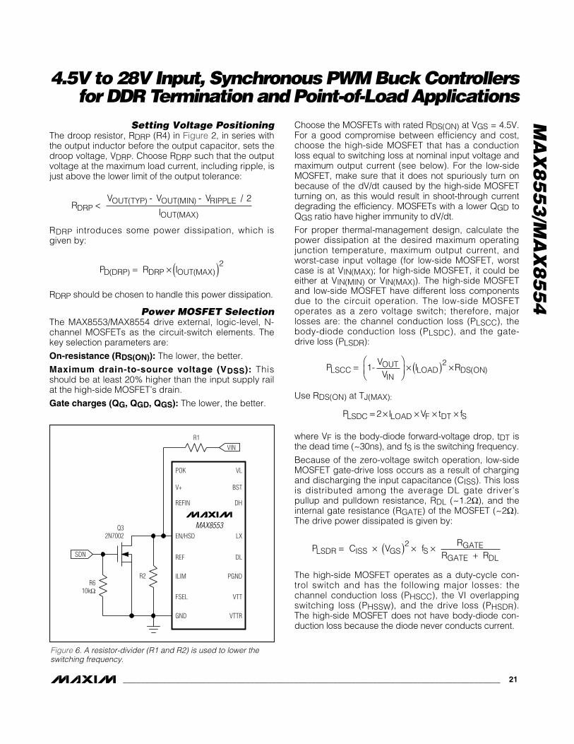
Adjusting the Switching FrequencyThe switching frequency of the MAX8553/MAX8554 canbe lowered from the value set by FSEL by adding aresistor voltage-divider to EN/HSD (HSD) as shown inFigure 6. This voltage-divider lowers the voltage the ICmeasures on EN/HSD (HSD), which increases the on-time. The switching frequency with the added resistor-divider is calculated as follows:
where K = 1.7µs and N is given in Tables 1 and 2. To setthe frequency, select a value for R2 between 10kΩ and100kΩ, then calculate R1 from the following equation:
With the minimum input voltage, make sure that thevoltage present at EN/HSD (HSD) is greater than 1.5Vwhen the resistor-divider is used:
V R
R RVIN MIN( )
.
×+
>2
1 21 5
R
K NRf
RS
11 2
2=×
× -
f
K NR
R RS ≅×
×+
1 2
1 2
( )
( )R
R I P R
V R I PILIM
DS ON VALLEY FB FOBK
OUT DS ON VALLEY FB=
× × × ( ) ×
× × × ( )( )10 1
10 1
-
- -
R
P VA PFOBK
FB OUT
FB=
×( )
5 1µ -
R
IA
RILIMVALLEY
DS ON= × × ( )105µ
MA
X8
55
3/M
AX
85
54
4.5V to 28V Input, Synchronous PWM Buck Controllersfor DDR Termination and Point-of-Load Applications
20 ______________________________________________________________________________________
MAX8553
DH
RILIM
RFOBK
VOUT
LX
DL
PGNDILIM
Figure 5. Setting the Foldback Current Limit with TwoResistors, RILIM and RFOBK
MA
X8
55
3/M
AX
85
54
4.5V to 28V Input, Synchronous PWM Buck Controllersfor DDR Termination and Point-of-Load Applications
______________________________________________________________________________________ 21
Setting Voltage PositioningThe droop resistor, RDRP (R4) in Figure 2, in series withthe output inductor before the output capacitor, sets thedroop voltage, VDRP. Choose RDRP such that the outputvoltage at the maximum load current, including ripple, isjust above the lower limit of the output tolerance:
RDRP introduces some power dissipation, which isgiven by:
RDRP should be chosen to handle this power dissipation.
Power MOSFET SelectionThe MAX8553/MAX8554 drive external, logic-level, N-channel MOSFETs as the circuit-switch elements. Thekey selection parameters are:
On-resistance (RDS(ON)): The lower, the better.
Maximum drain-to-source voltage (VDSS): Thisshould be at least 20% higher than the input supply railat the high-side MOSFET’s drain.
Gate charges (QG, QGD, QGS): The lower, the better.
Choose the MOSFETs with rated RDS(ON) at VGS = 4.5V.For a good compromise between efficiency and cost,choose the high-side MOSFET that has a conductionloss equal to switching loss at nominal input voltage andmaximum output current (see below). For the low-sideMOSFET, make sure that it does not spuriously turn onbecause of the dV/dt caused by the high-side MOSFETturning on, as this would result in shoot-through currentdegrading the efficiency. MOSFETs with a lower QGD toQGS ratio have higher immunity to dV/dt.
For proper thermal-management design, calculate thepower dissipation at the desired maximum operatingjunction temperature, maximum output current, andworst-case input voltage (for low-side MOSFET, worstcase is at VIN(MAX); for high-side MOSFET, it could beeither at VIN(MIN) or VIN(MAX)). The high-side MOSFETand low-side MOSFET have different loss componentsdue to the circuit operation. The low-side MOSFEToperates as a zero voltage switch; therefore, majorlosses are: the channel conduction loss (PLSCC), thebody-diode conduction loss (PLSDC), and the gate-drive loss (PLSDR):
Use RDS(ON) at TJ(MAX):
where VF is the body-diode forward-voltage drop, tDT isthe dead time (~30ns), and fS is the switching frequency.
Because of the zero-voltage switch operation, low-sideMOSFET gate-drive loss occurs as a result of chargingand discharging the input capacitance (CISS). This lossis distributed among the average DL gate driver’spullup and pulldown resistance, RDL (~1.2Ω), and theinternal gate resistance (RGATE) of the MOSFET (~2Ω).The drive power dissipated is given by:
The high-side MOSFET operates as a duty-cycle con-trol switch and has the following major losses: thechannel conduction loss (PHSCC), the VI overlappingswitching loss (PHSSW), and the drive loss (PHSDR).The high-side MOSFET does not have body-diode con-duction loss because the diode never conducts current.
P C V f
RR RLSDR ISS GS S
GATE
GATE DL= × ( ) × ×
+
2
P I V t fLSDC LOAD F DT S= × × × ×2
P
VV
I RLSCCOUT
INLOAD DS ON=
× ( ) × ( )1 2-
P R ID DRP DRP OUT MAX( ) ( ) = × ( )2
RV V V
IDRPOUT TYP OUT MIN RIPPLE
OUT MAX<
/ ( ) ( )
( )
- - 2
MAX8553
GND
FSEL
ILIM
REF
EN/HSD
REFIN
V+
POK
VTTR
VTT
PGND
DL
LX
DH
BST
VL
R2R6
10kΩ
Q32N7002
SDN
R1VIN
Figure 6. A resistor-divider (R1 and R2) is used to lower theswitching frequency.

Use RDS(ON) at TJ(MAX):
where IGATE is the average DH driver output currentdetermined by:
where RDH is the high-side MOSFET driver’s on-resis-tance (1.4Ω typ) and RGATE is the internal gate resis-tance of the MOSFET (~2Ω):
where VGS = VVL = 5V.
When the MAX8553 is sinking current, the high-sideMOSFET operates as a zero-voltage switch and thelow-side MOSFETs operate as a nonzero-voltageswitch.
In addition to the losses above, allow about 20% morefor additional losses due to MOSFET output capaci-tances and low-side MOSFET body-diode reverserecovery charge dissipated in the high-side MOSFETthat is not well defined in the MOSFET data sheet. Referto the MOSFET data sheet for thermal-resistance speci-fications to calculate the PC board area needed tomaintain the desired maximum operating junction tem-perature with the above calculated power dissipations.
To reduce EMI caused by switching noise, add a 0.1µFceramic capacitor from the high-side switch drain tothe low-side switch source, or add resistors in serieswith DH and DL to slow down the switching transitions.Adding series resistors increases the power dissipationof the MOSFET, so ensure that this does not overheatthe MOSFET.
Control IC Power DissipationPower dissipation in the MAX8553/MAX8554 IC is pri-marily due to the on-chip MOSFETs’ gate drivers (DHand DL). This power dissipation depends on the gatecharge of the external MOSFETs used. Power dissipa-tion in the MAX8553 also depends on the VTTR loadcurrent (IVTTR). Use the following equation to calculatethe power dissipation:
where QGH and QGL are the total gate charge of thehigh-side and low-side MOSFETs, respectively. Selectthe switching frequency and VV+ correctly to ensurethe power dissipation does not exceed the packagepower-dissipation requirement.
Applications InformationPC Board Layout
A properly designed PC board layout is important inany switching regulator. The switching power stagerequires particular attention. If possible, mount all thepower components on the top-side of the board withtheir ground terminals flush against one another. Followthese guidelines for good PC board layout:
1) Keep the high-current paths short, especially at theground terminals. This practice is essential for sta-ble, low-jitter operation.
2) Connect GND and PGND together at a single point.
3) Keep the power traces and load connections short.This practice is essential for high efficiency. The useof thick copper PC boards (2oz vs. 1oz) can notice-ably enhance full-load efficiency. Correctly routingPC board traces is a difficult task that must beapproached in terms of fractions of centimeters,where a single mΩ of excess trace resistance caus-es a measurable efficiency penalty.
4) LX and PGND connections to the low-side MOSFETfor current limiting must be made using Kelvin-sense connections in order to guarantee the cur-rent-limit accuracy. With 8-pin SO MOSFETs, thiscan be done by routing power to the MOSFETs from
P V f Q Q ID V S GH GL VTTR= ( ) × × +( ) +[ ]+
P Q V fR
R RHSDR G GS SGATE
GATE DH= × × ×
+
IV
R RGATEDH GATE
=+2 5.
P V I f
Q QIHSSW IN LOAD S
GS GD
GATE= × × × +
P
VV
I RHSCCOUT
INLOAD DS ON= × ( ) × ( )
2
MA
X8
55
3/M
AX
85
54
4.5V to 28V Input, Synchronous PWM Buck Controllersfor DDR Termination and Point-of-Load Applications
22 ______________________________________________________________________________________

MA
X8
55
3/M
AX
85
54
4.5V to 28V Input, Synchronous PWM Buck Controllersfor DDR Termination and Point-of-Load Applications
______________________________________________________________________________________ 23
Pin Configurations
outside using the top copper layer, while tying inPGND and LX inside (underneath) the 8-pin SOpackage.
5) When trade-offs in trace lengths must be made, it ispreferable to allow the inductor charging path to bemade longer than the discharge path. For example,it is better to allow some extra distance between theinput capacitors and the high-side MOSFET than toallow distance between the inductor and the low-side MOSFET or between the inductor and the out-put filter capacitor.
6) It may be desirable to deliberately introduce sometrace length (droop resistance) between the FBinductor node and the output filter capacitor tomeet the stability criteria (fESR < fS / π).
7) Place feedback resistors as close as possible tothe IC.
8) Route high-speed switching nodes away from sen-sitive analog nodes.
9) Make all pin-strap control input connections (ILIM,etc.) to GND or VL close to the chip, and do notconnect to PGND.
Chip InformationTRANSISTOR COUNT: 2827
PROCESS: BiCMOS
16
15
14
13
12
11
10
9
1
2
3
4
5
6
7
8
EN/HSD LX
DH
BST
PGND
DL
VL
V+
VTTR
TOP VIEW
MAX8553
QSOP
REFIN
POK
FSEL
VTT
ILIM
REF
GND
16
15
14
13
12
11
10
9
1
2
3
4
5
6
7
8
HSD LX
DH
BST
PGND
DL
VL
V+
OUT
MAX8554
QSOP
EN
POK
FSEL
FB
ILIM
REF
GND
MA
X8
55
3/M
AX
85
54
4.5V to 28V Input, Synchronous PWM Buck Controllersfor DDR Termination and Point-of-Load Applications
Maxim cannot assume responsibility for use of any circuitry other than circuitry entirely embodied in a Maxim product. No circuit patent licenses areimplied. Maxim reserves the right to change the circuitry and specifications without notice at any time.
24 ____________________Maxim Integrated Products, 120 San Gabriel Drive, Sunnyvale, CA 94086 408-737-7600
© 2005 Maxim Integrated Products Printed USA is a registered trademark of Maxim Integrated Products, Inc.
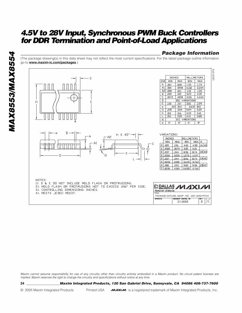
Package Information(The package drawing(s) in this data sheet may not reflect the most current specifications. For the latest package outline informationgo to www.maxim-ic.com/packages.)
QS
OP
.EP
S
E1
121-0055
PACKAGE OUTLINE, QSOP .150", .025" LEAD PITCH