DC-Voltage-Ratio Control Strategy for Multilevel Cascaded Converters Fed With a Single DC Source
9
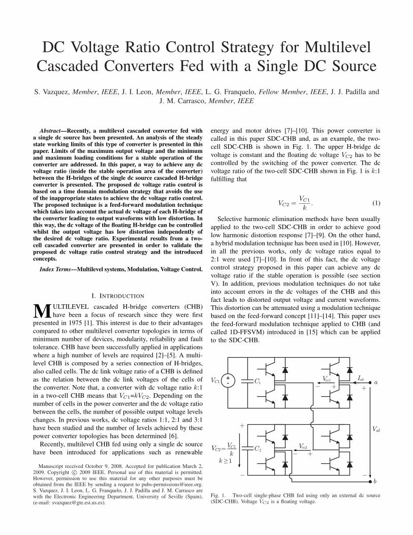
DC Voltage Ratio Control Strategy for Multilevel Cascaded Converters Fed with a Single DC Source S. Vazquez, Member, IEEE, J. I. Leon, Member, IEEE, L. G. Franquelo, Fellow Member, IEEE, J. J. Padilla and J. M. Carrasco, Member, IEEE Abstract—Recently, a multilevel cascaded converter fed with a single dc source has been presented. An analysis of the steady state working limits of this type of converter is presented in this paper. Limits of the maximum output voltage and the minimum and maximum loading conditions for a stable operation of the converter are addressed. In this paper, a way to achieve any dc voltage ratio (inside the stable operation area of the converter) between the H-bridges of the single dc source cascaded H-bridge converter is presented. The proposed dc voltage ratio control is based on a time domain modulation strategy that avoids the use of the inappropriate states to achieve the dc voltage ratio control. The proposed technique is a feed-forward modulation technique which takes into account the actual dc voltage of each H-bridge of the converter leading to output waveforms with low distortion. In this way, the dc voltage of the floating H-bridge can be controlled whilst the output voltage has low distortion independently of the desired dc voltage ratio. Experimental results from a two- cell cascaded converter are presented in order to validate the proposed dc voltage ratio control strategy and the introduced concepts. Index Terms—Multilevel systems, Modulation, Voltage Control. I. I NTRODUCTION M ULTILEVEL cascaded H-bridge converters (CHB) have been a focus of research since they were first presented in 1975 [1]. This interest is due to their advantages compared to other multilevel converter topologies in terms of minimum number of devices, modularity, reliability and fault tolerance. CHB have been successfully applied in applications where a high number of levels are required [2]–[5]. A multi- level CHB is composed by a series connection of H-bridges, also called cells. The dc link voltage ratio of a CHB is defined as the relation between the dc link voltages of the cells of the converter. Note that, a converter with dc voltage ratio k:1 in a two-cell CHB means that V C1 =kV C2 . Depending on the number of cells in the power converter and the dc voltage ratio between the cells, the number of possible output voltage levels changes. In previous works, dc voltage ratios 1:1, 2:1 and 3:1 have been studied and the number of levels achieved by these power converter topologies has been determined [6]. Recently, multilevel CHB fed using only a single dc source have been introduced for applications such as renewable Manuscript received October 9, 2008. Accepted for publication March 2, 2009. Copyright c 2009 IEEE. Personal use of this material is permitted. However, permission to use this material for any other purposes must be obtained from the IEEE by sending a request to [email protected]. S. Vazquez, J. I. Leon, L. G. Franquelo, J. J. Padilla and J. M. Carrasco are with the Electronic Engineering Department, University of Seville (Spain), (e-mail: [email protected]). energy and motor drives [7]–[10]. This power converter is called in this paper SDC-CHB and, as an example, the two- cell SDC-CHB is shown in Fig. 1. The upper H-bridge dc voltage is constant and the floating dc voltage V C2 has to be controlled by the switching of the power converter. The dc voltage ratio of the two-cell SDC-CHB shown in Fig. 1 is k:1 fulfilling that V C2 = V C1 k . (1) Selective harmonic elimination methods have been usually applied to the two-cell SDC-CHB in order to achieve good low harmonic distortion response [7]–[9]. On the other hand, a hybrid modulation technique has been used in [10]. However, in all the previous works, only dc voltage ratios equal to 2:1 were used [7]–[10]. In front of this fact, the dc voltage control strategy proposed in this paper can achieve any dc voltage ratio if the stable operation is possible (see section V). In addition, previous modulation techniques do not take into account errors in the dc voltages of the CHB and this fact leads to distorted output voltage and current waveforms. This distortion can be attenuated using a modulation technique based on the feed-forward concept [11]–[14]. This paper uses the feed-forward modulation technique applied to CHB (and called 1D-FFSVM) introduced in [15] which can be applied to the SDC-CHB. b C 1 C 2 a I ab V ab V C1 V C1 V C2 = k 1 - + - + + - V m1 + - V m2 k Fig. 1. Two-cell single-phase CHB fed using only an external dc source (SDC-CHB). Voltage V C2 is a floating voltage.
-
Upload
independent -
Category
Documents
-
view
1 -
download
0
Transcript of DC-Voltage-Ratio Control Strategy for Multilevel Cascaded Converters Fed With a Single DC Source
DC Voltage Ratio Control Strategy for MultilevelCascaded Converters Fed with a Single DC Source
S. Vazquez, Member, IEEE, J. I. Leon, Member, IEEE, L. G. Franquelo, Fellow Member, IEEE, J. J. Padilla andJ. M. Carrasco, Member, IEEE
Abstract—Recently, a multilevel cascaded converter fed witha single dc source has been presented. An analysis of the steadystate working limits of this type of converter is presented in thispaper. Limits of the maximum output voltage and the minimumand maximum loading conditions for a stable operation of theconverter are addressed. In this paper, a way to achieve any dcvoltage ratio (inside the stable operation area of the converter)between the H-bridges of the single dc source cascaded H-bridgeconverter is presented. The proposed dc voltage ratio control isbased on a time domain modulation strategy that avoids the useof the inappropriate states to achieve the dc voltage ratio control.The proposed technique is a feed-forward modulation techniquewhich takes into account the actual dc voltage of each H-bridge ofthe converter leading to output waveforms with low distortion. Inthis way, the dc voltage of the floating H-bridge can be controlledwhilst the output voltage has low distortion independently ofthe desired dc voltage ratio. Experimental results from a two-cell cascaded converter are presented in order to validate theproposed dc voltage ratio control strategy and the introducedconcepts.
Index Terms—Multilevel systems, Modulation, Voltage Control.
I. INTRODUCTION
MULTILEVEL cascaded H-bridge converters (CHB)have been a focus of research since they were first
presented in 1975 [1]. This interest is due to their advantagescompared to other multilevel converter topologies in terms ofminimum number of devices, modularity, reliability and faulttolerance. CHB have been successfully applied in applicationswhere a high number of levels are required [2]–[5]. A multi-level CHB is composed by a series connection of H-bridges,also called cells. The dc link voltage ratio of a CHB is definedas the relation between the dc link voltages of the cells ofthe converter. Note that, a converter with dc voltage ratio k:1in a two-cell CHB means that VC1=kVC2. Depending on thenumber of cells in the power converter and the dc voltage ratiobetween the cells, the number of possible output voltage levelschanges. In previous works, dc voltage ratios 1:1, 2:1 and 3:1have been studied and the number of levels achieved by thesepower converter topologies has been determined [6].
Recently, multilevel CHB fed using only a single dc sourcehave been introduced for applications such as renewable
Manuscript received October 9, 2008. Accepted for publication March 2,2009. Copyright c© 2009 IEEE. Personal use of this material is permitted.However, permission to use this material for any other purposes must beobtained from the IEEE by sending a request to [email protected]. Vazquez, J. I. Leon, L. G. Franquelo, J. J. Padilla and J. M. Carrasco arewith the Electronic Engineering Department, University of Seville (Spain),(e-mail: [email protected]).
energy and motor drives [7]–[10]. This power converter iscalled in this paper SDC-CHB and, as an example, the two-cell SDC-CHB is shown in Fig. 1. The upper H-bridge dcvoltage is constant and the floating dc voltage VC2 has to becontrolled by the switching of the power converter. The dcvoltage ratio of the two-cell SDC-CHB shown in Fig. 1 is k:1fulfilling that
VC2 =VC1
k. (1)
Selective harmonic elimination methods have been usuallyapplied to the two-cell SDC-CHB in order to achieve goodlow harmonic distortion response [7]–[9]. On the other hand,a hybrid modulation technique has been used in [10]. However,in all the previous works, only dc voltage ratios equal to2:1 were used [7]–[10]. In front of this fact, the dc voltagecontrol strategy proposed in this paper can achieve any dcvoltage ratio if the stable operation is possible (see sectionV). In addition, previous modulation techniques do not takeinto account errors in the dc voltages of the CHB and thisfact leads to distorted output voltage and current waveforms.This distortion can be attenuated using a modulation techniquebased on the feed-forward concept [11]–[14]. This paper usesthe feed-forward modulation technique applied to CHB (andcalled 1D-FFSVM) introduced in [15] which can be appliedto the SDC-CHB.
b
C1
C2
aIab
Vab
VC1
VC1VC2=
k 1
−
+
−
+
+−
Vm1
+−
Vm2
k
Fig. 1. Two-cell single-phase CHB fed using only an external dc source(SDC-CHB). Voltage VC2 is a floating voltage.
The structure of this paper is the following: In section II abrief introduction of the state of the art of the modulationtechniques for the SDC-CHB is addressed. In section III,the 1D-FFSVM technique is summarized. This technique isapplied in section IV where the proposed voltage control tech-nique depending on the desired voltage ratio k:1 is described.In order to complete the study and to determine the limits ofthe proposed dc voltage control strategy, an analysis of themaximum output phase voltage and the possible loading con-ditions that achieve a stable operation is presented in section V.The experimental results of the proposed modulation techniqueincluding the dc voltage ratio control are shown in section VI.Finally, in section VII the conclusions of the proposed workare addressed.
II. MODULATION TECHNIQUES AND DC VOLTAGE RATIOCONTROL FOR MULTILEVEL CHB AND SDC-CHB
Different multilevel modulation techniques for CHB havebeen presented in the literature. Many of these techniques havebeen extended from classic pulse width modulation (PWM)[16], [17], space-vector modulation (SVM) methods [18]–[21]and selective harmonic elimination (SHE) techniques [22]–[25]. Related with the SDC-CHB topology, previous workshave used SHE techniques with a reduced number of switchingangles [7], [8] or hybrid modulation techniques reducing thecommutations of the fixed dc voltage H-bridge of the converter[10]. All these modulation techniques achieve good resultsobtaining good harmonic spectrum results and controlling thefloating dc voltage.
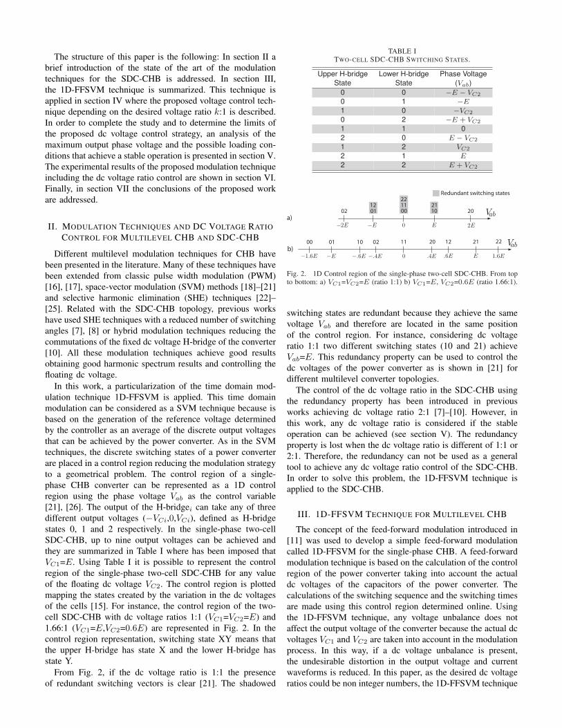
In this work, a particularization of the time domain mod-ulation technique 1D-FFSVM is applied. This time domainmodulation can be considered as a SVM technique because isbased on the generation of the reference voltage determinedby the controller as an average of the discrete output voltagesthat can be achieved by the power converter. As in the SVMtechniques, the discrete switching states of a power converterare placed in a control region reducing the modulation strategyto a geometrical problem. The control region of a single-phase CHB converter can be represented as a 1D controlregion using the phase voltage Vab as the control variable[21], [26]. The output of the H-bridgei can take any of threedifferent output voltages (−VCi,0,VCi), defined as H-bridgestates 0, 1 and 2 respectively. In the single-phase two-cellSDC-CHB, up to nine output voltages can be achieved andthey are summarized in Table I where has been imposed thatVC1=E. Using Table I it is possible to represent the controlregion of the single-phase two-cell SDC-CHB for any valueof the floating dc voltage VC2. The control region is plottedmapping the states created by the variation in the dc voltagesof the cells [15]. For instance, the control region of the two-cell SDC-CHB with dc voltage ratios 1:1 (VC1=VC2=E) and1.66:1 (VC1=E,VC2=0.6E) are represented in Fig. 2. In thecontrol region representation, switching state XY means thatthe upper H-bridge has state X and the lower H-bridge hasstate Y.
From Fig. 2, if the dc voltage ratio is 1:1 the presenceof redundant switching vectors is clear [21]. The shadowed
TABLE ITWO-CELL SDC-CHB SWITCHING STATES.
Upper H-bridge Lower H-bridge Phase VoltageState State (Vab)
0 0 −E − VC2
0 1 −E1 0 −VC2
0 2 −E + VC2
1 1 02 0 E − VC2
1 2 VC2
2 1 E2 2 E + VC2
Redundant switching states
02 0112
001122
2110 20
−2E 0 2EEE
Vaba)
b)00 01 11
−1.6E 0−E
−
02
−.4E
10
−.6E 1.6EE.4E .6E
20 222112 Vab
Fig. 2. 1D Control region of the single-phase two-cell SDC-CHB. From topto bottom: a) VC1=VC2=E (ratio 1:1) b) VC1=E, VC2=0.6E (ratio 1.66:1).
switching states are redundant because they achieve the samevoltage Vab and therefore are located in the same positionof the control region. For instance, considering dc voltageratio 1:1 two different switching states (10 and 21) achieveVab=E. This redundancy property can be used to control thedc voltages of the power converter as is shown in [21] fordifferent multilevel converter topologies.
The control of the dc voltage ratio in the SDC-CHB usingthe redundancy property has been introduced in previousworks achieving dc voltage ratio 2:1 [7]–[10]. However, inthis work, any dc voltage ratio is considered if the stableoperation can be achieved (see section V). The redundancyproperty is lost when the dc voltage ratio is different of 1:1 or2:1. Therefore, the redundancy can not be used as a generaltool to achieve any dc voltage ratio control of the SDC-CHB.In order to solve this problem, the 1D-FFSVM technique isapplied to the SDC-CHB.
III. 1D-FFSVM TECHNIQUE FOR MULTILEVEL CHB
The concept of the feed-forward modulation introduced in[11] was used to develop a simple feed-forward modulationcalled 1D-FFSVM for the single-phase CHB. A feed-forwardmodulation technique is based on the calculation of the controlregion of the power converter taking into account the actualdc voltages of the capacitors of the power converter. Thecalculations of the switching sequence and the switching timesare made using this control region determined online. Usingthe 1D-FFSVM technique, any voltage unbalance does notaffect the output voltage of the converter because the actual dcvoltages VC1 and VC2 are taken into account in the modulationprocess. In this way, if a dc voltage unbalance is present,the undesirable distortion in the output voltage and currentwaveforms is reduced. In this paper, as the desired dc voltageratios could be non integer numbers, the 1D-FFSVM technique
is very suitable to be applied to the two-cell SDC-CHB. Inthis way, the desired output sinusoidal waveforms with lowdistortion are generated for any value of the desired dc voltageratio. The 1D-FFSVM technique has been used in this paper.In order to make the paper self-contained and to improve theclarity of the text, a summary of the 1D-FFSVM technique ispresented.
The 1D-FFSVM technique determines several factors k1, k2
and k3 depending on the actual dc voltage values of the CHBas is summarized in Table II. In this table, factor ρ is definedas
ρ =1
VC1 + VC2. (2)
In [15], the dc voltage ratio control of a two-cell single-phase CHB is studied in detail. Different cases have to bestudied depending on the actual values of the dc voltages andthe sign of the phase current Iab. The effect of each switchingstate on the dc voltages is well known and is applied tomultilevel converters along with the concept of the redundantvectors in the SVM strategies to control the dc voltages ofthe dc link in different multilevel converter topologies. Inthe 1D control regions of the 1D-FFSVM technique with dcvoltage ratio control, the switching states of the converter thatlead to increase the voltage unbalance have been eliminatedand therefore are reduced versions of the general 1D controlregions. Table III is used to define all the cases when thedesired dc voltage ratio is 1:1 (cases from A to H). In addition,in Table III the desired evolution of the dc voltages of the CHBis shown in the fourth column. This information is useful whenthe dc voltage ratio k:1 (k different of 1 is studied).
For each case (from A to H), reduced versions of the 1Dcontrol regions similar to those presented in Fig. 2 have to beused to determine the switching sequence and the switchingtimes. Once the 1D control region to be considered is known,the 1D-FFSVM technique with dc voltage ratio control carriesout a normalization of the phase voltage Vab obtaining factora as
TABLE IIki FACTORS DEFINITIONS [15]
DC Voltage ki factorsCondition expression
VC2 < VC1 ≤ 2VC2
k1 = ρ(VC1 − VC2)
k2 = ρVC2
k3 = ρVC1
VC1 > 2VC2
k1 = ρVC2
k2 = ρ(VC1 − VC2)
k3 = ρVC1
VC1 < VC2 ≤ 2VC1
k1 = ρ(VC2 − VC1)
k2 = ρVC1
k3 = ρVC2
VC2 > 2VC1
k1 = ρVC1
k2 = ρ(VC2 − VC1)
k3 = ρVC2
TABLE IIICASES OF STUDY OF THE DC VOLTAGE RATIO CONTROL STRATEGY WITH
DC VOLTAGE RATIO 1:1 [15]
Phase Actual dc Voltage Desired dcCurrent dc Voltage Ratio 1:1 Voltage Condition
Condition Condition Case V ∗C1,V ∗C2
Iab > 0
VC2 < VC1 ≤ 2VC2 Case A ↓, ↑VC1 > 2VC2 Case B ↓, ↑
VC1 < VC2 ≤ 2VC1 Case C ↑, ↓VC2 > 2VC1 Case D ↑, ↓
Iab ≤ 0
VC2 < VC1 ≤ 2VC2 Case E ↓, ↑VC1 > 2VC2 Case F ↓, ↑
VC1 < VC2 ≤ 2VC1 Case G ↑, ↓VC2 > 2VC1 Case H ↑, ↓
TABLE IVSWITCHING SEQUENCE AND SWITCHING TIMES FOR CASE A [15]
ConditionSwitching Switching Times
Sequence (t2 = 1− t1)
−k3 > a ≥ −1 01-00 t1 = a+11−k3
−k1 > a ≥ −k3 02-01 t1 = a+k3k3−k1
0 > a ≥ −k1 11-02 t1 = a+k1k1
k2 > a ≥ 0 12-11 t1 = ak2
1 ≥ a ≥ k2 22-12 t1 = a−k21−k2
a =Vab
VC1 + VC2= ρVab. (3)
Using the factors k1, k2 and k3 defined in Table II, anddepending on the unbalance case from A to H determinedin Table III, an iterative geometrical search of factor a inthe resulting reduced 1D control region finally determines theswitching sequence and the switching times. The switchingsequence is formed by the two nearest switching states ofthe 1D control region. As an example, the results obtainedfor case A are summarized in Table IV. Similar tables wereobtained for all the cases [15]. All the determined switchingsequences generates the desired phase voltage Vab whilst thedc voltages tend to be controlled towards their desired values.The calculations involved in the process are very simple.
IV. DC VOLTAGE RATIO CONTROL FOR MULTILEVELSDC-CHB
The aim of this paper is to control any dc voltage ratiousing a SDC-CHB always fulfilling that VC1 ≥ VC2. As wasmentioned in section II previous works have demonstratedthat some specific dc voltage ratios can be controlled choos-ing properly the redundant switching states in the switchingsequence. DC voltage ratios different of 1:1 or 2:1 are notcontrolled because the redundancy property is lost. In thispaper, using the 1D-FFSVM technique and the proposed dcvoltage ratio control method any dc voltage ratio can beachieved. However, it should be noticed that the controllabilityof the system has to be studied because it depends on the
desired dc voltage ratio and the power factor as is addressedin section V.
The proposed way to control the balance of the dc voltageof the floating cell of the two-cell SDC-CHB inverter is similarto the technique to carry out the dc voltage control for the two-cell CHB acting as a synchronous rectifier. As was mentionedbefore, this technique is based on the exclusion of the inappro-priate states in the switching sequence regardless of whetheror not they are redundant. In this paper, a generalization of themethod is presented in order to achieve any dc voltage ratiousing the two-cell SDC-CHB acting as an inverter.
A. Target: DC voltage ratio 1:1
In this section of the paper the control objective is to havethe same voltage in each cell of the SDC-CHB. The dc voltagecontrol method summarized in previous section is directlyapplied to the two-cell SDC-CHB. The determination of theswitching sequence and the switching times follows the nextsteps:
1) Determination of the ki factors using Table II.2) Determination of the unbalance case (from A to H) using
Table III.3) Normalization of the desired phase voltage V ∗
ab usingexpression (3) obtaining factor a.
4) Geometrical search of factor a in the reduced 1D controlregion. The switching sequence and the switching timesare calculated using tables similar to Table IV dependingon the unbalance case (from A to H) [15]. These tablesdescribe the modulation strategies related to 1D controlregions similar to those shown in Fig. 2 where some ofthe switching states have been eliminated because theytend to unbalance the dc voltages of a multilevel CHB.Therefore, the same modulation strategy can be used tocontrol the dc voltage of the two-cell SDC-CHB.
B. Target: DC voltage ratio k:1
Taking into account any current and voltage condition, anycase considering the dc voltage ratio k:1 can be reduced toa case present on the dc voltage ratio 1:1 study (cases fromA to H) summarized in Table III. Depending on the desiredvalue of the dc voltage ratio k, Table V or Table VI has to beused to achieve the dc voltage ratio target. Table V shows thecase 2 > k ≥ 1 and Table VI shows the case k ≥ 2.
In order to understand these tables, several examples areshown. Firstly, let’s assume that the desired dc voltage ratiois 1.5:1, the phase current Iab is positive and the actual dcvoltage unbalance fulfills that VC2 < VC1 ≤ 1.5VC2. Theseconditions included in those defined for case A in Table III fora desired dc voltage ratio equal to 1:1. Under these voltage andcurrent assumptions, it can be noticed that it is desired that VC1
increases and VC2 decreases to achieve the 1.5:1 dc voltageratio. These desired dc voltage conditions (VC1 ↑, VC2 ↓),shown in the fourth column of Table V, do not coincide withthe desired dc voltage conditions of case A in Table III whereit is desired completely the opposite. Cases A, B, C and Dhave opposite effects on the dc voltage values compared withcases E, F, G and H respectively. Therefore, in the example
TABLE VCASES OF STUDY OF THE DC VOLTAGE RATIO CONTROL STRATEGY WITH
DC VOLTAGE RATIO k : 1, 1 ≤ k < 2
Phase Actual Associated Desired dc
Current dc Voltage dc Voltage Voltage Condition
Condition Condition Ratio 1:1 Case V ∗C1,V ∗C2
Iab > 0
VC2 < VC1 ≤ kVC2 Case E ↑, ↓2VC2 ≥ VC1 > kVC2 Case A ↓, ↑
VC1 > 2VC2 Case B ↓, ↑VC1 < VC2 ≤ 2VC1 Case C ↑, ↓
VC2 > 2VC1 Case D ↑, ↓
Iab ≤ 0
VC2 < VC1 ≤ kVC2 Case G ↑, ↓2VC2 ≥ VC1 > kVC2 Case E ↓, ↑
VC1 > 2VC2 Case F ↓, ↑VC1 < VC2 ≤ 2VC1 Case G ↓, ↑
VC2 > 2VC1 Case H ↑, ↓
TABLE VICASES OF STUDY OF THE DC VOLTAGE RATIO CONTROL STRATEGY WITH
DC VOLTAGE RATIO k : 1, k ≥ 2
Phase Actual Associated Desired dc
Current dc Voltage dc Voltage Voltage Condition
Condition Condition Ratio 1:1 Case V ∗C1,V ∗C2
Iab > 0
VC2 < VC1 ≤ 2VC2 Case E ↑, ↓kVC2 ≥ VC1 > 2VC2 Case F ↑, ↓
VC1 > kVC2 Case B ↓, ↑VC1 < VC2 ≤ 2VC1 Case C ↑, ↓
VC2 > 2VC1 Case D ↑, ↓
Iab ≤ 0
VC2 < VC1 ≤ 2VC2 Case A ↑, ↓kVC2 ≥ VC1 > 2VC2 Case B ↑, ↓
VC1 > kVC2 Case F ↓, ↑VC1 < VC2 ≤ 2VC1 Case G ↑, ↓
VC2 > 2VC1 Case H ↑, ↓
case, the final case to be applied is case E in order to fulfillwith the desired dc voltage conditions (VC1 ↑, VC2 ↓).
On the other hand, let’s assume in a second example thatthe desired dc voltage ratio is 1.5:1, the phase current Iab
is positive and the actual dc voltage unbalance fulfills that2VC2 ≥ VC1 > kVC2. This dc voltage condition also isincluded in case A in Table III for a desired dc voltageratio equal to 1:1. In this second example, the desired dcvoltage conditions, shown in the fourth column of Table V,are (VC1 ↓, VC2 ↑) what coincides with the desired dc voltageconditions of case A in Table III. Therefore, the case to beapplied in order to tend to the desired dc voltage ratio 1.5:1 iscase A. All the cases for desired dc voltage ratios k:1 canbe studied using similar considerations and the results aresummarized in Table V and Table VI.
Finally, as a summary, the determination of the switchingsequence and the switching times to achieve an specific desireddc voltage ratio k:1 follows the next steps:
1) Determination of the ki factors using Table II.2) Determination of the unbalance case (from A to H) using
Table V or Table VI depending on the value of thedesired dc voltage ratio k.
3) Normalization of the desired phase voltage V ∗ab using
expression 3 obtaining factor a.4) The switching sequence and the switching times are
calculated using tables similar to Table IV dependingon the unbalance case (from A to H).
As can be observed, the step 2 is the only difference betweenthe dc voltage ratio 1:1 case and any dc voltage ratio k:1.
The proposed technique can be extended to SDC-CHB withmore than two H-bridges. The required study to extend theproposed modulation technique for SDC-CHB with highernumber of power cells rises proportionally in complexity, sincethe number of cases to be analyzed increases. However, thisstudy can be done offline writing similar tables compared withthose obtained for the two-cell SDC-CHB case. However, itshould be noticed that the online calculations needed to exe-cute the corresponding modulation technique do not increasesignificantly. This fact was also reported for the 1D-FFSVMtechnique in [15].
V. ANALYSIS OF THE CONTROLLABILITY OF THESDC-CHB
An analysis of the performance of the SDC-CHB in termsof the limits of the output phase voltage and loading conditionsis presented in this section. The fundamental harmonic of theoutput phase voltage (Vab,1), the fundamental harmonic of thephase current (Iab,1) and the fundamental harmonic of theoutput voltage of each H-bridge (Vm1,1,Vm2,1) are consideredin this analysis. A phasorial representation, as in [27], isused plotting the RMS values of these magnitudes definedrespectively as vab, iab, v1 and v2. As Vab=Vm1+Vm2, it isfulfilled that Vab,1=Vm1,1+Vm2,1 and vab=v1+v2. In addition,in these phasorial diagrams, the maximum output voltages inRMS of each H-bridge can be calculated as
vc1 =2√
2π
VC1
vc2 =2√
2π
VC2. (4)
A. Output voltage analysis
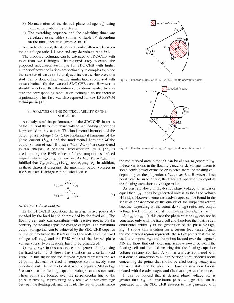
In the SDC-CHB operation, the average active power de-manded by the load has to be provided by the fixed cell. Thefloating cell only can contribute with reactive power, on thecontrary the floating capacitor voltage changes. The maximumoutput voltage that can be achieved by the SDC-CHB dependson the ratio between the RMS value of the voltage of the fixedvoltage cell (vc1) and the RMS value of the desired phasevoltage (vab). Two situations have to be considered:
1) vc1 ≥ vab: In this case vab can be generated only usingthe fixed cell. Fig. 3 shows this situation for a certain loadvalue. In this figure the red marked region represents the setof points that can be used to compose vab. In steady stateoperation, only the points located over the segment MN in Fig.3 ensure that the floating capacitor voltage remains constant.These points are located over the perpendicular line to thephase current iab representing only reactive power exchangebetween the floating cell and the load. The rest of points inside
Reachable area
vabφiab
M
N
vc1
vc2
Fig. 3. Reachable area when vc1 ≥ vab. Stable operation points.
Reachable area
φM
N
vab
vc1
vc2
iab
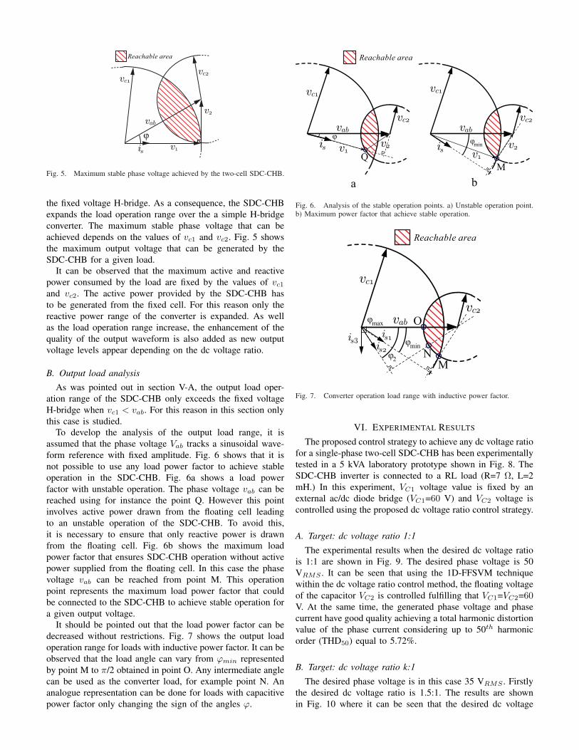
Fig. 4. Reachable area when vc1 < vab. Stable operation points.
the red marked area, although can be chosen to generate vab,induce variations in the floating capacitor dc voltage. There issome active power extracted or injected from the floating cell,depending on the projection of vc2 over iab. However, thesepoints can be used during the transient operation to regulatethe floating capacitor dc voltage value.
As was said above, if the desired phase voltage vab is less orequal than vc1, it can be generated only with the fixed voltageH-bridge. However, some extra advantages can be found in thesense of enhancement of the quality of the output waveformbecause, depending on the actual dc voltage ratio, new outputvoltage levels can be used if the floating H-bridge is used.
2) vc1 < vab: In this case the phase voltage vab can not begenerated only with the fixed cell and therefore the floating cellcontributes critically in the generation of the phase voltage.Fig. 4 shows this situation for a certain load value. Againthe red marked region represents the set of points that can beused to compose vab, and the points located over the segmentMN are those that only exchange reactive power between thefloating cell and the load ensuring that the floating capacitorvoltage remains constant. A similar analysis compared withthat done in subsection V-A1 can be done. Similar conclusionsconcerning the points that should be used during steady andtransient state can be obtained. However new conclusionsrelated with the advantages and disadvantages can be done.
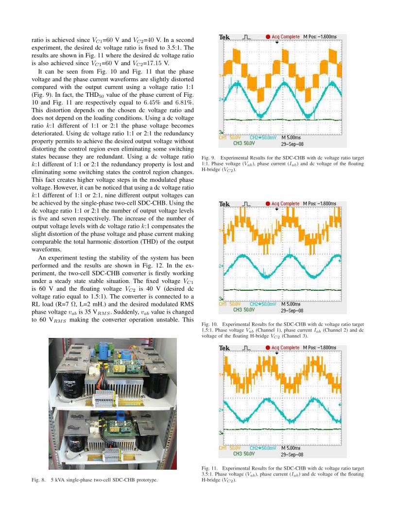
It can be noticed that if desired phase voltage vab isgreater than vc1, the maximum phase voltage that can begenerated with the SDC-CHB exceeds to that generated with
Reachable area
φ
vc1vc2
v2
v1is
vab
Fig. 5. Maximum stable phase voltage achieved by the two-cell SDC-CHB.
the fixed voltage H-bridge. As a consequence, the SDC-CHBexpands the load operation range over the a simple H-bridgeconverter. The maximum stable phase voltage that can beachieved depends on the values of vc1 and vc2. Fig. 5 showsthe maximum output voltage that can be generated by theSDC-CHB for a given load.
It can be observed that the maximum active and reactivepower consumed by the load are fixed by the values of vc1
and vc2. The active power provided by the SDC-CHB hasto be generated from the fixed cell. For this reason only thereactive power range of the converter is expanded. As wellas the load operation range increase, the enhancement of thequality of the output waveform is also added as new outputvoltage levels appear depending on the dc voltage ratio.
B. Output load analysis
As was pointed out in section V-A, the output load oper-ation range of the SDC-CHB only exceeds the fixed voltageH-bridge when vc1 < vab. For this reason in this section onlythis case is studied.
To develop the analysis of the output load range, it isassumed that the phase voltage Vab tracks a sinusoidal wave-form reference with fixed amplitude. Fig. 6 shows that it isnot possible to use any load power factor to achieve stableoperation in the SDC-CHB. Fig. 6a shows a load powerfactor with unstable operation. The phase voltage vab can bereached using for instance the point Q. However this pointinvolves active power drawn from the floating cell leadingto an unstable operation of the SDC-CHB. To avoid this,it is necessary to ensure that only reactive power is drawnfrom the floating cell. Fig. 6b shows the maximum loadpower factor that ensures SDC-CHB operation without activepower supplied from the floating cell. In this case the phasevoltage vab can be reached from point M. This operationpoint represents the maximum load power factor that couldbe connected to the SDC-CHB to achieve stable operation fora given output voltage.
It should be pointed out that the load power factor can bedecreased without restrictions. Fig. 7 shows the output loadoperation range for loads with inductive power factor. It can beobserved that the load angle can vary from ϕmin representedby point M to π/2 obtained in point O. Any intermediate anglecan be used as the converter load, for example point N. Ananalogue representation can be done for loads with capacitivepower factor only changing the sign of the angles ϕ.
Reachable area
Q
φ
M
φ
ba
min
vc1
vc2
vc1
vc2
is is
vab vab
v1
v2v2v1
Fig. 6. Analysis of the stable operation points. a) Unstable operation point.b) Maximum power factor that achieve stable operation.
Reachable area
NM
φmin
O
φ2
φmax
vc1
vab
vc2
is3is1is2
Fig. 7. Converter operation load range with inductive power factor.
VI. EXPERIMENTAL RESULTS
The proposed control strategy to achieve any dc voltage ratiofor a single-phase two-cell SDC-CHB has been experimentallytested in a 5 kVA laboratory prototype shown in Fig. 8. TheSDC-CHB inverter is connected to a RL load (R=7 Ω, L=2mH.) In this experiment, VC1 voltage value is fixed by anexternal ac/dc diode bridge (VC1=60 V) and VC2 voltage iscontrolled using the proposed dc voltage ratio control strategy.
A. Target: dc voltage ratio 1:1
The experimental results when the desired dc voltage ratiois 1:1 are shown in Fig. 9. The desired phase voltage is 50VRMS . It can be seen that using the 1D-FFSVM techniquewithin the dc voltage ratio control method, the floating voltageof the capacitor VC2 is controlled fulfilling that VC1=VC2=60V. At the same time, the generated phase voltage and phasecurrent have good quality achieving a total harmonic distortionvalue of the phase current considering up to 50th harmonicorder (THD50) equal to 5.72%.
B. Target: dc voltage ratio k:1
The desired phase voltage is in this case 35 VRMS . Firstlythe desired dc voltage ratio is 1.5:1. The results are shownin Fig. 10 where it can be seen that the desired dc voltage
ratio is achieved since VC1=60 V and VC2=40 V. In a secondexperiment, the desired dc voltage ratio is fixed to 3.5:1. Theresults are shown in Fig. 11 where the desired dc voltage ratiois also achieved since VC1=60 V and VC2=17.15 V.
It can be seen from Fig. 10 and Fig. 11 that the phasevoltage and the phase current waveforms are slightly distortedcompared with the output current using a voltage ratio 1:1(Fig. 9). In fact, the THD50 value of the phase current of Fig.10 and Fig. 11 are respectively equal to 6.45% and 6.81%.This distortion depends on the chosen dc voltage ratio anddoes not depend on the loading conditions. Using a dc voltageratio k:1 different of 1:1 or 2:1 the phase voltage becomesdeteriorated. Using dc voltage ratio 1:1 or 2:1 the redundancyproperty permits to achieve the desired output voltage withoutdistorting the control region even eliminating some switchingstates because they are redundant. Using a dc voltage ratiok:1 different of 1:1 or 2:1 the redundancy property is lost andeliminating some switching states the control region changes.This fact creates higher voltage steps in the modulated phasevoltage. However, it can be noticed that using a dc voltage ratiok:1 different of 1:1 or 2:1, nine different output voltages canbe achieved by the single-phase two-cell SDC-CHB. Using thedc voltage ratio 1:1 or 2:1 the number of output voltage levelsis five and seven respectively. The increase of the number ofoutput voltage levels with dc voltage ratio k:1 compensates theslight distortion of the phase voltage and phase current makingcomparable the total harmonic distortion (THD) of the outputwaveforms.
An experiment testing the stability of the system has beenperformed and the results are shown in Fig. 12. In the ex-periment, the two-cell SDC-CHB converter is firstly workingunder a steady state stable situation. The fixed voltage VC1
is 60 V and the floating voltage VC2 is 40 V (desired dcvoltage ratio equal to 1.5:1). The converter is connected to aRL load (R=7 Ω, L=2 mH.) and the desired modulated RMSphase voltage vab is 35 VRMS . Suddenly, vab value is changedto 60 VRMS making the converter operation unstable. This
Fig. 8. 5 kVA single-phase two-cell SDC-CHB prototype.
Fig. 9. Experimental Results for the SDC-CHB with dc voltage ratio target1:1. Phase voltage (Vab), phase current (Iab) and dc voltage of the floatingH-bridge (VC2).
Fig. 10. Experimental Results for the SDC-CHB with dc voltage ratio target1.5:1. Phase voltage Vab (Channel 1), phase current Iab (Channel 2) and dcvoltage of the floating H-bridge VC2 (Channel 3).
Fig. 11. Experimental Results for the SDC-CHB with dc voltage ratio target3.5:1. Phase voltage (Vab), phase current (Iab) and dc voltage of the floatingH-bridge (VC2).
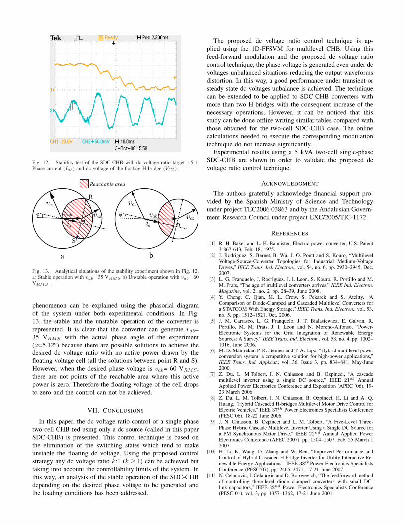
Fig. 12. Stability test of the SDC-CHB with dc voltage ratio target 1.5:1.Phase current (Iab) and dc voltage of the floating H-bridge (VC2).
Reachable area
vc1vc1
vc2vc2
isis
vab vab
S
R
φφ
ba
Fig. 13. Analytical situations of the stability experiment shown in Fig. 12.a) Stable operation with vab= 35 VRMS b) Unstable operation with vab= 60VRMS .
phenomenon can be explained using the phasorial diagramof the system under both experimental conditions. In Fig.13, the stable and the unstable operation of the converter isrepresented. It is clear that the converter can generate vab=35 VRMS with the actual phase angle of the experiment(ϕ=5.12o) because there are possible solutions to achieve thedesired dc voltage ratio with no active power drawn by thefloating voltage cell (all the solutions between point R and S).However, when the desired phase voltage is vab= 60 VRMS ,there are not points of the reachable area where this activepower is zero. Therefore the floating voltage of the cell dropsto zero and the control can not be achieved.
VII. CONCLUSIONS
In this paper, the dc voltage ratio control of a single-phasetwo-cell CHB fed using only a dc source (called in this paperSDC-CHB) is presented. This control technique is based onthe elimination of the switching states which tend to makeunstable the floating dc voltage. Using the proposed controlstrategy any dc voltage ratio k:1 (k ≥ 1) can be achieved buttaking into account the controllability limits of the system. Inthis way, an analysis of the stable operation of the SDC-CHBdepending on the desired phase voltage to be generated andthe loading conditions has been addressed.
The proposed dc voltage ratio control technique is ap-plied using the 1D-FFSVM for multilevel CHB. Using thisfeed-forward modulation and the proposed dc voltage ratiocontrol technique, the phase voltage is generated even under dcvoltages unbalanced situations reducing the output waveformsdistortion. In this way, a good performance under transient orsteady state dc voltages unbalance is achieved. The techniquecan be extended to be applied to SDC-CHB converters withmore than two H-bridges with the consequent increase of thenecessary operations. However, it can be noticed that thisstudy can be done offline writing similar tables compared withthose obtained for the two-cell SDC-CHB case. The onlinecalculations needed to execute the corresponding modulationtechnique do not increase significantly.
Experimental results using a 5 kVA two-cell single-phaseSDC-CHB are shown in order to validate the proposed dcvoltage ratio control technique.
ACKNOWLEDGMENT
The authors gratefully acknowledge financial support pro-vided by the Spanish Ministry of Science and Technologyunder project TEC2006-03863 and by the Andalusian Govern-ment Research Council under project EXC/2005/TIC-1172.
REFERENCES
[1] R. H. Baker and L. H. Bannister, Electric power converter, U.S. Patent3 867 643, Feb. 18, 1975.
[2] J. Rodriguez, S. Bernet, B. Wu, J. O. Pontt and S. Kouro, “MultilevelVoltage-Source-Converter Topologies for Industrial Medium-VoltageDrives,” IEEE Trans. Ind. Electron., vol. 54, no. 6, pp. 2930–2945, Dec.2007.
[3] L. G. Franquelo, J. Rodriguez, J. I. Leon, S. Kouro, R. Portillo and M.M. Prats, “The age of multilevel converters arrives,” IEEE Ind. Electron.Magazine, vol. 2, no. 2, pp. 28–39, June 2008.
[4] Y. Cheng, C. Qian, M. L. Crow, S. Pekarek and S. Atcitty, “AComparison of Diode-Clamped and Cascaded Multilevel Converters fora STATCOM With Energy Storage,” IEEE Trans. Ind. Electron., vol. 53,no. 5, pp. 1512–1521, Oct. 2006.
[5] J. M. Carrasco, L. G. Franquelo, J. T. Bialasiewicz, E. Galvan, R.Portillo, M. M. Prats, J. I. Leon and N. Moreno-Alfonso, “Power-Electronic Systems for the Grid Integration of Renewable EnergySources: A Survey,” IEEE Trans. Ind. Electron., vol. 53, no. 4, pp. 1002–1016, June 2006.
[6] M. D. Manjrekar, P. K. Steimer and T. A. Lipo, “Hybrid multilevel powerconversion system: a competitive solution for high-power applications,”IEEE Trans. Ind. Applicat., vol. 36, Issue 3, pp. 834–841, May-June2000.
[7] Z. Du, L. M.Tolbert, J. N. Chiasson and B. Ozpineci, “A cascademultilevel inverter using a single DC source,” IEEE 21st AnnualApplied Power Electronics Conference and Exposition (APEC ’06), 19-23 March 2006.
[8] Z. Du, L. M. Tolbert, J. N. Chiasson, B. Ozpineci, H. Li and A. Q.Huang, “Hybrid Cascaded H-bridges Multilevel Motor Drive Control forElectric Vehicles,” IEEE 37th Power Electronics Specialists Conference(PESC’06), 18-22 June 2006.
[9] J. N. Chiasson, B. Ozpineci and L. M. Tolbert, “A Five-Level Three-Phase Hybrid Cascade Multilevel Inverter Using a Single DC Source fora PM Synchronous Motor Drive,” IEEE 22nd Annual Applied PowerElectronics Conference (APEC 2007), pp. 1504–1507, Feb. 25-March 12007.
[10] H. Li, K. Wang, D. Zhang and W. Ren, “Improved Performance andControl of Hybrid Cascaded H-bridge Inverter for Utility Interactive Re-newable Energy Applications,” IEEE 38thPower Electronics SpecialistsConference (PESC’07), pp. 2465–2471, 17-21 June 2007.
[11] N. Celanovic, I. Celanovic and D. Boroyevich, “The feedforward methodof controlling three-level diode clamped converters with small DC-link capacitors,” IEEE 32nd Power Electronics Specialists Conference(PESC’01), vol. 3, pp. 1357–1362, 17-21 June 2001.
[12] J. Pou, D. Boroyevich and R. Pindado, “New feedforward space-vectorPWM method to obtain balanced AC output voltages in a three-levelneutral-point-clamped converter,” IEEE Trans. Ind. Electron., vol. 49,no. 5, pp. 1026–1034, Oct. 2002.
[13] S. Kouro, P. Lezana, M. Angulo and J. Rodriguez, “Multicarrier PWMwith DC-Link Ripple Feedforward Compensation for Multilevel Invert-ers,” IEEE Trans. Power Electron., vol. 23, no. 1, pp. 52–59, Jan. 2008.
[14] J. I. Leon, S. Vazquez, R. Portillo, L. G. Franquelo, J. M. Carrasco,P. W. Wheeler, A. J. Watson, “Three-Dimensional Feed-Forward SpaceVector Modulation Applied to Multilevel Diode-Clamped Converters,”IEEE Trans. Ind. Electron., in press.
[15] J. I. Leon, S. Vazquez, A. J. Watson, P. W. Wheeler, L. G. Franqueloand J. M. Carrasco, “Feed-forward Space Vector Modulation for Single-Phase Multilevel Cascade Converters with any DC voltage ratio,” IEEETrans. Ind. Electron., in press.
[16] G. Carrara, S. Gardella, M. Marchesoni, R. Salutari and G. Sciutto, “Anew multilevel pwm method: A theoretical analysis,” IEEE Trans. PowerElectron., vol. 7, no. 3, pp. 497–505, July 1992.
[17] B. P. McGrath and D. G. Holmes, “Multicarrier PWM strategies formultilevel inverters,” IEEE Trans. Ind. Electron., vol. 49, no. 4, pp.858–867, August 2002.
[18] A. K. Gupta and A. M. Khambadkone, “A space vector PWM schemefor multilevel inverters based on two-level space vector PWM,” IEEETrans. Ind. Electron., vol. 53, no. 5, pp. 1631–1639, Oct. 2006.
[19] N. Celanovic and D. Boroyevich, “A fast space-vector modulation algo-rithm for multilevel three-phase converters,” IEEE Trans. Ind. Applicat.,vol. 37, no. 2, pp. 637–641, Mar./Apr. 2001.
[20] C. Rech and J. R. Pinheiro, “Hybrid Multilevel Converters: UnifiedAnalysis and Design Considerations,” IEEE Trans. Ind. Electron., vol.54, no. 2, pp. 1092–1104, April 2007.
[21] J. I. Leon, R. Portillo, S. Vazquez, J. J. Padilla, L. G. Franqueloand J. M. Carrasco, “Simple Unified Approach to Develop a TimeDomain Modulation Strategy for Single-Phase Multilevel Converters,”IEEE Trans. Ind. Electron., vol. 55, no. 9, pp. 3239–3248, Sept. 2008.
[22] H. S. Patel and R. G. Hoft, “Generalized techniques of harmonicelimination and voltage control in thyristor inverters-Part 1: Harmonicelimination,” IEEE Trans. Ind. Applicat., vol. IA-9, pp. 310–317,May/June 1973.
[23] V. G. Agelidis, A. I. Balouktsis and C. Cossar, “On Attaining theMultiple Solutions of Selective Harmonic Elimination PWM Three-Level Waveforms Through Function Minimization,” IEEE Trans. Ind.Electron., vol. 55, no. 3, pp. 996–1004, March 2008.
[24] Z. Du, L. M. Tolbert, J. N. Chiasson and B. Ozpineci, “ReducedSwitching-Frequency Active Harmonic Elimination for Multilevel Con-verters,” IEEE Trans. Ind. Electron., vol. 55, no. 4, pp. 1761–1770, April2008.
[25] A. J. Watson, P. W. Wheeler and J. C. Clare, “A Complete HarmonicElimination Approach to DC Link Voltage Balancing for a CascadedMultilevel Rectifier,” IEEE Trans. Ind. Electron., vol. 54, no. 6, pp.2946–2953, Dec. 2007.
[26] J. I. Leon, R. Portillo, L. G. Franquelo, S. Vazquez, J. M. Carrasco and E.Domınguez, “New space vector modulation technique for single-phasemultilevel converters,” IEEE International Symposium on IndustrialElectronics (ISIE’07), pp. 617–622, 4–7 June 2007.
[27] S. Vazquez, J. I. Leon, J. M. Carrasco, L. G. Franquelo, E. Galvan, J.A. Sanchez and E. Dominguez “Controller Design for a Single-PhaseTwo-Cell Multilevel Cascade H-bridge Converter,” IEEE InternationalSymposium on Industrial Electronics, 2008 (ISIE 2008), pp. 1–6, June30–July 2 2008.
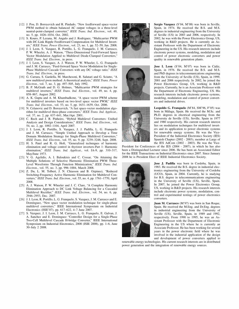
Sergio Vazquez (S’04, M’08) was born in Seville,Spain, in 1974. He received the B.S. and M.S.degrees in industrial engineering from the Universityof Seville (US) in 2003 and 2006, respectively. In2002, he was with the Power Electronics Group, US,working in R&D projects. He is currently an As-sistant Professor with the Department of ElectronicEngineering in the US. His research interests includeelectronic power systems, modeling, modulation andcontrol of power electronic converters and powerquality in renewable generation plants.
Jose I. Leon (S’04, M’07) was born in Cadiz,Spain, in 1976. He received the B.S. and M.S.and PhD degrees in telecommunications engineeringfrom the University of Seville (US), Spain, in 1999,2001 and 2006 respectively. In 2002, he joined thePower Electronics Group, US, working in R&Dprojects. Currently, he is an Associate Professor withthe Department of Electronic Engineering, US. Hisresearch interests include electronic power systems,modeling, modulation and control of power convert-ers and industrial drives.
Leopoldo G. Franquelo (M’84, SM’96, F’05) wasborn in Malaga, Spain. He received the M.Sc. andPh.D. degrees in electrical engineering from theUniversity de Seville (US), Seville, Spain in 1977and 1980 respectively. His current research interestlies on modulation techniques for multilevel invert-ers and its application to power electronic systemsfor renewable energy systems. He was the Vice-President of the Industrial Electronics Society (IES)Spanish Chapter (2002 - 2003), member at Large ofthe IES AdCom (2002 - 2003). He was the Vice-
President for Conferences of the IES (2004 - 2007), in which he has alsobeen a Distinguished Lecturer since 2006. He has been an Associated Editorfor the IEEE Transactions on Industrial Electronics since 2007. Since January2008 he is President Elect of IEEE Industrial Electronics Society.
Jose J. Padilla was born in Cordoba, Spain, in1983. He received the B.S. degree in industrial elec-tronics engineering from the University of Cordoba(UCO), Spain, in 2004. Currently, he is studyingfor B.S. degree in telecommunications engineeringin the University of Seville (US), Seville, Spain.In 2007, he joined the Power Electronics Group,US, working in R&D projects. His research interestsinclude electronic power systems, modulation, con-trol and experimental testings of power electronicsconverters.
Juan M. Carrasco (M’97) was born in San Roque,Spain. He received the M.Eng. and Dr.Eng. degreesin industrial engineering from the University ofSeville (US), Seville, Spain, in 1989 and 1992,respectively. From 1990 to 1995, he was an As-sistant Professor with the Department of ElectronicEngineering in the US where he is currently anAssociate Professor. He has been working for severalyears in the power electronic field where he wasinvolved in the industrial application of the designand development of power converters applied to
renewable energy technologies. His current research interests are in distributedpower generation and the integration of renewable energy sources.