Dynamic Analysis of Cascaded Laser Power Converters for Simultaneous High-Speed Data Detection and...
8
IEEE TRANSACTIONS ON ELECTRON DEVICES, VOL. 58, NO. 7, JULY 2011 2049 Dynamic Analysis of Cascaded Laser Power Converters for Simultaneous High-Speed Data Detection and Optical-to-Electrical DC Power Generation Jin-Wei Shi, F.-M. Kuo, Chan-Shan Yang, S.-S. Lo, and Ci-Ling Pan, Senior Member, IEEE Abstract—We analyze the dynamic behaviors of a novel device, i.e., cascaded high-speed laser power converters (LPCs), which can detect the direct-current (dc) component of an incoming high- speed optical data stream and efficiently convert its dc component to dc electrical power. By utilizing a p-type photoabsorption layer in our LPC, the problem of slow-motion holes can be eliminated, and only the electrons act as the active carriers. We can thus achieve high-speed performance with the LPC under forward- bias operation with a small electric field inside. Furthermore, according to our modeling and measurement results, there are a significant alternating-current capacitance reduction and an electron-trapping effect at the interface between the absorption and collector layers with a significant degradation in the carrier drift velocity. These become more serious with the increase in optical pumping power and forward-bias voltage and truly limit the net optical-to-electrical (O–E) bandwidth of the device. In order to overcome such a transient-time-limited bandwidth and further increase the maximum dc output voltage of the LPC, we connect two single LPCs in series (cascade). Error-free data detection of 10-Gb/s and an O–E dc power-generation efficiency of 21.1% can be achieved simultaneously at a wavelength of 850 nm by the use of such two cascaded LPCs. Index Terms—Photodiodes (PDs), photovoltaic. I. I NTRODUCTION R ECENTLY, thedevelopment of optical-interconnect (OI) techniques [1]–[4], which could allow the replacement of bulky and power-hungry active/passive microwave compo- nents with more energy-saving and high-speed optoelectronic Manuscript received January 21, 2011; revised March 21, 2011 and March 23, 2011; accepted March 25, 2011. Date of publication April 21, 2011; date of current version June 22, 2011. This work was supported in part by the National Science Council of Taiwan under Grant 99-2221-E-008-027-MY3 and Grant 98-2221-E-008-009-MY3 and in part by the Ministry of Economic Affairs of Taiwan under Grant 98-EC-17-A-07-S1-001. The review of this paper was arranged by Editor A. G. Aberle. J.-W. Shi and F.-M. Kuo are with the Department of Electrical Engineer- ing, National Central University, Taoyuan 320, Taiwan, and also with the Department of Electrical and Computer Engineering, University of California Santa Barbara, Santa Barbara, CA 93106 USA (e-mail: [email protected]; [email protected]). C.-S. Yang and C.-L. Pan are with the Department of Physics, National Tsing Hua University, Hsinchu 300, Taiwan. S.-S. Lo is with the Department of Photonics and Institute of Electro-Optics, National Chiao Tung University, Hsinchu 300, Taiwan. Color versions of one or more of the figures in this paper are available online at http://ieeexplore.ieee.org. Digital Object Identifier 10.1109/TED.2011.2136379 devices, has become an attractive choice to realize the ideal of the “Green Internet” [5]. In exascale supercomputers, the OI technique plays a key role in meeting challenging technologi- cal and economic requirements. In future supercomputers, the estimated total power consumption and bandwidth for an OI system could be as high as 8 MW and 400 PB/s, respectively [6]. The reduction of the power required to feed the high- speed vertical-cavity surface-emitting laser (VCSEL) at the transmitting end is one effective way to further reduce the over- all power consumption. On the other hand, the direct-current (dc) component of the high-speed optical data signal at the receiving end is usually wasted due to the fact that, in traditional p-i-n photodiodes (PDs), reverse-bias operation is necessary, which will result in the power consumption with excess heat generation during high-speed optical data detection. Recently, the unitraveling-carrier PD (UTC PD) structure has been used to achieve reasonable high-speed and high-responsivity perfor- mance under zero-bias operation [7]–[9]. Such devices have been demonstrated to eliminate the excess power consumption. In this paper, we analyze in detail the dynamic behaviors of a novel device, i.e., the linear cascaded GaAs/AlGaAs-based high-speed laser power converter (LPC) [10]–[13], by the use of the equivalent-circuit modeling technique [14]. Such a device exhibits the performance of a high-speed PD even when its operating voltage is further pushed to the forward bias. We can thus generate (instead of consuming) dc electrical power by using this device during high-speed data transmission in an OI system. By the use of the equivalent-circuit modeling technique, we found that the significant alternating-current (ac) capacitance reduction effect happens [14] and the slow internal carrier transient time is the dominant bandwidth-limiting factor of a single LPC under a forward-bias voltage of > 0.5 V. In order to further boost the operating speed and maximum output dc voltage of our device, we connect two single LPCs in series. According to the modeling result, our cascaded structure can effectively minimize the internal carrier drift time. This is due to the larger built-in field compared with that of a single LPC even when operated under the same output current and forward bias (i.e., +1 V). Error-free optical data detection of 10 Gb/s (or 5 Gb/s) with an optical-to-electrical (O–E) power- generation efficiency of 21.1% (or 34%) can be simultaneously achieved using our device with the cascaded structure at an optical wavelength of 850 nm. 0018-9383/$26.00 © 2011 IEEE
-
Upload
independent -
Category
Documents
-
view
7 -
download
0
Transcript of Dynamic Analysis of Cascaded Laser Power Converters for Simultaneous High-Speed Data Detection and...

IEEE TRANSACTIONS ON ELECTRON DEVICES, VOL. 58, NO. 7, JULY 2011 2049
Dynamic Analysis of Cascaded Laser PowerConverters for Simultaneous High-SpeedData Detection and Optical-to-Electrical
DC Power GenerationJin-Wei Shi, F.-M. Kuo, Chan-Shan Yang, S.-S. Lo, and Ci-Ling Pan, Senior Member, IEEE
Abstract—We analyze the dynamic behaviors of a novel device,i.e., cascaded high-speed laser power converters (LPCs), whichcan detect the direct-current (dc) component of an incoming high-speed optical data stream and efficiently convert its dc componentto dc electrical power. By utilizing a p-type photoabsorption layerin our LPC, the problem of slow-motion holes can be eliminated,and only the electrons act as the active carriers. We can thusachieve high-speed performance with the LPC under forward-bias operation with a small electric field inside. Furthermore,according to our modeling and measurement results, there area significant alternating-current capacitance reduction and anelectron-trapping effect at the interface between the absorptionand collector layers with a significant degradation in the carrierdrift velocity. These become more serious with the increase inoptical pumping power and forward-bias voltage and truly limitthe net optical-to-electrical (O–E) bandwidth of the device. Inorder to overcome such a transient-time-limited bandwidth andfurther increase the maximum dc output voltage of the LPC,we connect two single LPCs in series (cascade). Error-free datadetection of 10-Gb/s and an O–E dc power-generation efficiency of21.1% can be achieved simultaneously at a wavelength of 850 nmby the use of such two cascaded LPCs.
Index Terms—Photodiodes (PDs), photovoltaic.
I. INTRODUCTION
R ECENTLY, the development of optical-interconnect (OI)techniques [1]–[4], which could allow the replacement
of bulky and power-hungry active/passive microwave compo-nents with more energy-saving and high-speed optoelectronic
Manuscript received January 21, 2011; revised March 21, 2011 andMarch 23, 2011; accepted March 25, 2011. Date of publication April 21, 2011;date of current version June 22, 2011. This work was supported in part bythe National Science Council of Taiwan under Grant 99-2221-E-008-027-MY3and Grant 98-2221-E-008-009-MY3 and in part by the Ministry of EconomicAffairs of Taiwan under Grant 98-EC-17-A-07-S1-001. The review of thispaper was arranged by Editor A. G. Aberle.
J.-W. Shi and F.-M. Kuo are with the Department of Electrical Engineer-ing, National Central University, Taoyuan 320, Taiwan, and also with theDepartment of Electrical and Computer Engineering, University of CaliforniaSanta Barbara, Santa Barbara, CA 93106 USA (e-mail: [email protected];[email protected]).
C.-S. Yang and C.-L. Pan are with the Department of Physics, National TsingHua University, Hsinchu 300, Taiwan.
S.-S. Lo is with the Department of Photonics and Institute of Electro-Optics,National Chiao Tung University, Hsinchu 300, Taiwan.
Color versions of one or more of the figures in this paper are available onlineat http://ieeexplore.ieee.org.
Digital Object Identifier 10.1109/TED.2011.2136379
devices, has become an attractive choice to realize the ideal ofthe “Green Internet” [5]. In exascale supercomputers, the OItechnique plays a key role in meeting challenging technologi-cal and economic requirements. In future supercomputers, theestimated total power consumption and bandwidth for an OIsystem could be as high as 8 MW and 400 PB/s, respectively[6]. The reduction of the power required to feed the high-speed vertical-cavity surface-emitting laser (VCSEL) at thetransmitting end is one effective way to further reduce the over-all power consumption. On the other hand, the direct-current(dc) component of the high-speed optical data signal at thereceiving end is usually wasted due to the fact that, in traditionalp-i-n photodiodes (PDs), reverse-bias operation is necessary,which will result in the power consumption with excess heatgeneration during high-speed optical data detection. Recently,the unitraveling-carrier PD (UTC PD) structure has been usedto achieve reasonable high-speed and high-responsivity perfor-mance under zero-bias operation [7]–[9]. Such devices havebeen demonstrated to eliminate the excess power consumption.In this paper, we analyze in detail the dynamic behaviors ofa novel device, i.e., the linear cascaded GaAs/AlGaAs-basedhigh-speed laser power converter (LPC) [10]–[13], by the useof the equivalent-circuit modeling technique [14]. Such a deviceexhibits the performance of a high-speed PD even when itsoperating voltage is further pushed to the forward bias. Wecan thus generate (instead of consuming) dc electrical powerby using this device during high-speed data transmission inan OI system. By the use of the equivalent-circuit modelingtechnique, we found that the significant alternating-current (ac)capacitance reduction effect happens [14] and the slow internalcarrier transient time is the dominant bandwidth-limiting factorof a single LPC under a forward-bias voltage of > 0.5 V.In order to further boost the operating speed and maximumoutput dc voltage of our device, we connect two single LPCs inseries. According to the modeling result, our cascaded structurecan effectively minimize the internal carrier drift time. This isdue to the larger built-in field compared with that of a singleLPC even when operated under the same output current andforward bias (i.e., +1 V). Error-free optical data detection of10 Gb/s (or 5 Gb/s) with an optical-to-electrical (O–E) power-generation efficiency of 21.1% (or 34%) can be simultaneouslyachieved using our device with the cascaded structure at anoptical wavelength of 850 nm.
0018-9383/$26.00 © 2011 IEEE
2050 IEEE TRANSACTIONS ON ELECTRON DEVICES, VOL. 58, NO. 7, JULY 2011
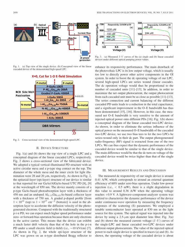
Fig. 1. (a) Top view of the single device. (b) Conceptual view of the linearcascaded device of the demonstrated high-speed LPC.
Fig. 2. Cross-sectional view of the demonstrated high-speed LPC.
II. DEVICE STRUCTURE
Fig. 1(a) and (b) shows the top view of a single LPC and aconceptual diagram of the linear cascaded LPCs, respectively.Fig. 2 shows a cross-sectional view of the fabricated device.We adopted a typical vertical-illuminated PD structure with anactive circular mesa and a p-type ring contact on the top. Thediameter of the whole mesa and the inner circle for light illu-mination were 28 and 20 μm, respectively. As shown in Fig. 2,the epitaxial-layer (epi-layer) structure of our device is similarto that reported for our GaAs/AlGaAs-based UTC PD [8], [9]at the wavelength of 850 nm. The device mainly consists of ap-type GaAs-based photoabsorption layer with a thickness of450 nm and an undoped Al0.15Ga0.85As-based collector layerwith a thickness of 750 nm. A graded p-doped profile [from1 × 1019 (top) to 1 × 1017 cm−3 (bottom)] is used in the ab-sorption layer to accelerate the diffusion velocity of the photo-generated electrons. Compared with the traditionally structuredp-i-n PD, we can expect much higher speed performance underzero- or forward-bias operation because there are only electronsin the active carrier. This means that the device can exhibita much faster drift velocity than that of the hole in the p-i-nPD under a small electric field (e-field) (i.e., ∼10 kV/cm) [7].As shown in Fig. 2, the whole epi-layer structure of theLPC was grown on an n-type distributed Bragg reflector to
Fig. 3. (a) Measured I–V curves of the (a) single and (b) linear cascadeddevices under different optical pumping power values.
enhance its responsivity performance. The main drawback ofthe photovoltaic LPC is its low output voltage, which is usuallytoo low to directly power other active components in the OIsystem. In order to boost the dc operating voltage of our LPC,several high-speed LPCs are series wound (linear cascade).The dc operation voltage would thus be proportional to thenumber of cascaded units [11]–[13]. In addition, in order tomaximize the net output photocurrent, the output photocurrentfrom each cascaded unit must be as close as possible [11]–[13].The series connection and current balancing of the differentcascaded PD units leads to a reduction in the total capacitance,and a significant improvement in the O–E bandwidth has thusbeen demonstrated [15], [16]. However, in this case, the mea-sured net O–E bandwidth is very sensitive to the amount ofinjected optical power onto different PDs [16]. Fig. 1(b) showsa conceptual diagram of the linear cascaded two-LPC device.As shown, in order to eliminate the serious influence of theoptical power on the measured O–E bandwidth of the cascadedtwo-LPC device, we use two bias tees to let the two LPCs beseries-wound only in their dc part. The output photogeneratedradio-frequency (RF) signal is extracted from one of the twoLPCs. We can thus expect that the dynamic performance of thecascaded device would be similar to that of the single device.The main difference would be that the dc turn-on voltage of thecascaded device would be twice higher than that of the singledevice.
III. MEASUREMENT RESULTS AND DISCUSSION
The measured dc responsivity of our single device is around0.41 A/W, which corresponds to around an external quantumefficiency of 60% under zero-bias operation. Under low-powerinjection (i.e., < 0.5 mW), there is a slight degradation inthis value to around 0.36 A/W when the operating voltagereaches +0.9 V. A lightwave-component-analyzer system wasutilized to characterize the dynamic performance of the deviceunder continuous-wave operation by measuring the frequencyresponses of the scattering (S) parameters. We employed atunable semiconductor laser operated at 830 nm as the lightsource for this system. The optical signal was injected into thedevice by using a 2.5-μm spot diameter lens fiber. Fig. 3(a)and (b) shows the measured current–voltage (I–V ) curves ofthe single-LPC and linear cascaded two-LPC devices underdifferent output photocurrents. The value of the injected opticalpower to each single device is specified in traces (a) and (b). Asshown, the operating voltage of the cascaded device is about

SHI et al.: DYNAMIC ANALYSIS OF LPCs FOR DATA DETECTION AND POWER GENERATION 2051
Fig. 4. Measured O–E power-conversion efficiency versus bias voltage of(a) the single and (b) linear cascaded devices under different optical pumpingpower values.
Fig. 5. Measured 3-dB O–E bandwidth versus forward-bias voltage for thesingle device under different output photocurrents. The inset shows the mea-sured O–E frequency responses of the single device under forward- and reverse-bias voltages with a fixed output current of 50 µA.
twice higher than that of a single cell with around one half ofthe responsivity. This is because the optical power needs to beabout two times higher to feed each single cell in the cascadedstructure to generate the same amount of output photocurrent asthat of the single device. Fig. 4(a) and (b) shows the measuredO–E power-conversion efficiency versus bias voltage of thesingle- and two-LPC cascaded devices under different opticalpumping power values. As shown, the maximum O–E power-conversion efficiency of both devices under low pumping powerand optimum bias voltage is around 34%. On the other hand,when the injected optical power exceeds 0.5 mW, as shown inFigs. 3 and 4, a significant reduction in both the photocurrentand external efficiency can be observed.
This phenomenon is somewhat similar to the case of ourLPC, which has a smaller turn-on voltage, and can be at-tributed to the saturation of the device under high-optical-powerinjection. Under high-power injection, the space-charge fieldinduced by the photogenerated carriers, which has the samedirection as the external forward-bias voltage [17], should be-come stronger and aid the forward-bias operation of the device.We can thus observe that the forward-bias current, whichscreens the photocurrent and degrades the efficiency perfor-mance, increases more rapidly with the forward-bias voltage.Figs. 5 and 6 show the measured O–E bandwidths of 3 dBversus forward operating voltage of single and linear cascadedLPCs under different output photocurrents. The insets showthe typical measured O–E frequency responses of the single-and two-LPC linear cascaded devices under the same effectiveforward voltage (i.e., +0.5 and +1 V, which is half of the
Fig. 6. Measured 3-dB O–E bandwidth versus forward-bias voltage for thelinear cascaded device under different output photocurrents. The inset showsthe measured O–E frequency responses of the linear cascaded device underforward- and reverse-bias voltages with a fixed output current of 50 µA.
Fig. 7. Two-port small-signal equivalent-circuit model of our device, whereVCCS indicates the voltage-controlled current source.
turn-on voltage) and reverse-bias voltage (i.e., −3 and −6 V).During measurement of the cascaded LPCs, the ratio of in-jected optical power to the two devices is around 1:1.2. Thephotogenerated signal was picked up from the PD with smallerinjected power. It is shown that there is a significant bandwidthdegradation for both devices with an increase in the forwardbias (0 to +2 V) and the output photocurrent (i.e., 50 μA toaround 0.5 mA). In addition, the linear cascaded LPCs exhibitsa faster speed performance than the single PD under the sameeffective bias voltage, as shown in the insets in Fig. 6.
Under a bias of +1 V and an output photocurrent of 50 μAof the linear cascaded LPC, which corresponds to the bias of+0.5 V for the single device, the measured bandwidths of 3 dBfor the cascaded and single devices are around 9 and 6 GHz,respectively. Even when the output photocurrent of the linearcascaded device reaches 0.2 mA at an operating voltage of+1 V, a 7.6-GHz 3-dB bandwidth can still be sustain. This isa clear indication of the capability of our linear cascaded LPCfor 10-Gb/s data transmission under a bias voltage of +1 V.The equivalent-circuit modeling technique is used to investigatethe mechanism for the observed bandwidth degradation in bothdevices under near the turn-on forward bias and the bandwidthenhancement effect with the cascaded device. Fig. 7 shows theestablished two-port equivalent-circuit model. Regions 1 and 2in this model represent the bandwidth limitation of the carriertransit time ft and resistive–capacitive (RC) delay time fRC,respectively [14], [16]. The artificial RC network [i.e., RT , CT ,and I(f)] in port 1 of region 1 represents the carrier transit-time effect. The S21 parameter is equivalent to the net O–Efrequency response [14], [16], and the S22 parameter of region 2determines the RC-limited frequency response of the device.

2052 IEEE TRANSACTIONS ON ELECTRON DEVICES, VOL. 58, NO. 7, JULY 2011
TABLE ILIST OF VALUES OF ELEMENTS USED IN THE FITTING PROCESS IN THE EQUIVALENT-CIRCUIT MODEL OF
OUR DEVICE UNDER A LOW OUTPUT PHOTOCURRENT (0.05 mA)
TABLE IILIST OF VALUES OF ELEMENTS USED IN THE FITTING PROCESS IN THE EQUIVALENT-CIRCUIT MODEL OF
OUR DEVICE UNDER HIGH OUTPUT PHOTOCURRENT (0.2 mA)
By assuming an ideal voltage-controlled current source (VCCS)(without the influence from (RT and CT ) in region 2), we canthus get the RC-limited frequency response for the device basedon the measured S22 parameter, as will be discussed in thefollowing. The physical meaning of each component in region2 has been detailed in our previous work [16].
The parameters for the “pad simulation” block include theparasitic effects of the coplanar-waveguide (CPW) pad inte-grated with the device active area. The S parameters for thisblock can be calculated using momentum simulation software[16]. The values for each circuit element in region 2 used inthe fitting process can be found in Tables I and II. These tablesshow the fitting parameters used under different forward-biasvoltages and low (0.05 mA) and high (0.2 mA) output photocur-rents, respectively. The contact resistance (Rs) values for eachdevice are chosen based on the measured differential resistance.In addition, the junction capacitance (Cc) values are chosenaccording to their active areas. As shown for both devices,such values become larger with an increase in the forward-biasvoltage due to the narrowing of the depletion width. The valuesof the parasitic capacitance Cp are determined by the overlay of
bottom n-type contact layers and the topmost connected metalsfrom the p-contact layer to the CPW pads. Figs. 8 and 9 showthe measured/fitted S22 parameters (from near dc to 15 GHz) onthe Smith chart under these two different output photocurrents(i.e., 0.05 and 0.2 mA) and two forward-bias voltages (i.e.,0.5 and 1 V for the single device and 1 and 2 V for the cascadeddevice) for the single and linear cascaded devices. A broadbandnetwork analyzer (Agilent N5250C) is used to measure theelectrical S22 parameters of these devices.
As shown in Figs. 8 and 9, all simulation results agree wellwith the measured ones from 0.04 to 15 GHz based on theadopted parameters shown in Tables I and II. In addition, undera moderate forward-bias voltage (i.e., +1 V for the cascadeddevice and +0.5 V for the single device), all the measuredS22 parameters are close, which implies that both devices havea similar RC-limited bandwidth. This is because we pick upthe photogenerated RF signal from only one of the two LPCcascaded structures, as aforementioned, and the measurementresults should be similar with a single LPC. On the other hand,when the forward bias reaches near the turn-on voltage (+2 Vfor the cascaded device and +1 V for the single device), as

SHI et al.: DYNAMIC ANALYSIS OF LPCs FOR DATA DETECTION AND POWER GENERATION 2053
Fig. 8. Smith chart showing the measured (circles) and fitted (solid lines)S22 parameters for a single LPC under forward-bias voltages of (a) +0.5 and(b) +1 V. The output photocurrents in (a) and (b) are fixed at 0.2 and 0.05 mA.The direction of the arrowhead indicates the increase in sweeping frequency.
Fig. 9. Smith chart showing the measured (circles) and fitted (solid lines)S22 parameters for the linear cascaded device under forward-bias voltages of(a) +0.5 and (b) +1-V. The output photocurrents in (a) and (b) are both fixedat 0.2 and 0.05 mA. The direction of the arrowhead indicates the increase insweeping frequency.
shown in Figs. 8(b) and 9(b), the measured S22 traces do notstart from the open-circuit point on the Smith chart, due tothe increase in forward conduction current. This leads to areduction in the junction resistance Rc, as shown in Tables Iand II. With the exception of the interesting bias-dependentbehavior of the measured S22 parameters as aforementioned,the measured S22 parameter of the single device shows distinctpower-dependent behaviors, as shown in Fig. 8. We can clearlysee that, with the increase in the output photocurrent (0.05to 0.2 mA), the S22 traces on the Smith chart are closer tothose for the ideal open circuit than the measured S22 traceunder low-current operation (0.05 mA), which implies a sig-nificant improvement in the microwave characteristics of thedevice.
As shown in Tables I and II, there is a significant reduction inthe Cc values for the single device with the increase in its outputphotocurrent. This phenomenon seldom happens in the tradi-tional p-i-n PD but has been reported in our previous work aboutnear-ballistic unitraveling-carrier PDs (NBUTC PDs) [14]. InNBUTC PDs, the electrical field in the collector (depletion)layer is low enough to sustain an overshoot drift velocity evenunder a high reverse voltage (−3 V). A significant improvementin its RC-limited bandwidth with an increase in the outputphotocurrent has been observed, which can be attributed to the
Fig. 10. Simulated band diagram of our single device under a forward biasof +0.8 V without injection light. The zero point on the Y-axis represents theinterface between the air and the topmost p+ ohmic contact layer.
ac capacitance reduction effect [14], [18]. It means the subtrac-tion of the differential ac capacitance IC × (dτC/dVac) [14],[18], which is proportional to the current, from the junctioncapacitance Cc, where Vac is the output ac voltage, IC is thephotocurrent, and τc is the electron drift time. In the case of theNBUTC PD, this effect should be significant due to the fact thatunder near-ballistic transport, the variation of the drift velocity(i.e., time is τc) of the electron versus the electrical field Vac isobvious, according to the reported field-dependent electron driftvelocity of III–V semiconductors. Fig. 10 shows the simulatedband diagram and e-field distribution of our device under+0.8-V operation without the injection of optical power. Thissimulation is performed using a commercial computer-aideddesign (CAD) tool (ISE TCAD).1 The simulated 1-D e-fieldand electron potential distributions shown here are located onthe x = 0 axis of the device cross section, as shown in Fig. 2.As shown, the magnitude of the e-field in the Al0.15Ga0.85As-based collector layer is less than 10 kV/cm, which is close tothe critical e-field for the overshoot drift velocity of electronsin the Al0.15Ga0.85As layer [19]. We can thus expect thatany high output ac photocurrent (voltage)-induced space-chargefield should further screen the built-in e-field in the collectorlayer and greatly slow down the overshoot drift velocity ofthe electrons, which suggests that the ratio of electron drifttime (velocity) to ac voltage dτC/dVac should be large, andthere would be a significant ac capacitance reduction. Thisphenomenon accompanies an improved RC-limited bandwidthin the single device; however, there is still a serious degradationin the net O–E bandwidth, as shown in Figs. 5 and 6. This is dueto the fact that the dominant bandwidth-limiting factor is theinternal carrier transient time rather than the RC time constantunder forward bias, as will be discussed in the following.
On the other hand, for the cascaded devices, as shown inFig. 9, this phenomenon is not significant. This result can beattributed to an imbalance in the optical power injected intothe two cascaded devices (1:1.2), which causes the devicewith the lower injected optical power to suffer from a smallereffective dc or instantaneous ac forward voltage and a larger
1Synopsys, Inc., 700 East Middle field Rd., Mountain View, CA, 94043-4033, U.S.A.

2054 IEEE TRANSACTIONS ON ELECTRON DEVICES, VOL. 58, NO. 7, JULY 2011
Fig. 11. Extracted RC-limited frequency responses, internal carrier transient-time responses, and measured O–E frequency responses for the (a) singleand (b) cascaded devices under the same effective forward-bias voltage and(+0.5 V for the single device and +1 V for the cascade device) outputphotocurrent (0.05 mA).
Fig. 12. Measured O–E bandwidth, extracted RC bandwidth, and transient-time-limited 3-dB bandwidth versus forward-bias voltages for the single deviceunder (a) low (0.05 mA) and (b) high output photocurrents (0.2 mA).
built-in field compared with the device with a higher injectedpower. The larger built-in field should avoid the slowing downof the overshoot electron drift velocity and impede the accapacitance reduction effect as aforementioned. We can thusunderstand that the cascaded structure exhibits a higher O–Ebandwidth than that of the single device from zero bias tonear forward conduction, as shown in Figs. 5 and 6, due tothe faster internal carrier transient time. By using the extractedequivalent-circuit model in region 2, the RC-limited frequencyresponses, and the measured net O–E frequency responses,we can further determine the internal transient-time-limitedfrequency responses. Fig. 11(a) and (b) shows the extractednet RC-limited frequency responses, internal carrier transient-time frequency responses, and measured O–E responses of thesingle and cascaded devices under the same effective forward-bias voltage (+0.5 versus +1 V) and output photocurrent(0.05 mA). As shown, the faster speed performance of thecascaded device can be mainly attributed to the shorter internalcarrier transient time, as aforementioned. Figs. 12 and 13 showthe three aforementioned 3-dB bandwidths (i.e., O–E, RC, andtransient time) versus forward-bias voltages of the single andcascaded devices under low and high output photocurrents,respectively. Overall, based on the measurement and modelingresults, we can conclude that, when the output photocurrentof both devices reaches hundreds of microamperes (200 μAfor our case), the dominant bandwidth-limiting factor becomesthe internal carrier transient time. On the other hand, under alow output photocurrent (tens of microamperes), both the RCand internal transient time limit the measured O–E bandwidths.Furthermore, under a certain range of forward-bias voltagesand output photocurrents, a significant ac capacitance reduction
Fig. 13. Measured O–E bandwidth, extracted RC bandwidth, and transient-time-limited 3-dB bandwidth versus forward-bias voltages for the cascadeddevice under (a) low (0.05 mA) and (b) high output photocurrents (0.2 mA).
effect has been observed with the single device, which implies asignificant reduction in the electron overshoot drift velocity andimprovement in the RC-limited bandwidth. In addition, basedon the extracted transient-time-limited bandwidths, as shown inFig. 12, and the reported formulas for electron diffusion/drifttime in the UTC PD [7], we can further determine the effectivetransient time in the active layer of our device. Take a singledevice under a low output photocurrent (0.05 mA) for example.The extracted transient-time-limited 3-dB bandwidth is around10 GHz, which corresponds to an internal carrier transienttime around of 55 ps. However, by using the equations for theelectron drift/diffusion time given in [7], the minority electrondiffusion coefficient (100 cm2V · s) in p-type GaAs, electronthermal velocity (4.4 × 10⁵ m/s), and electron drift velocity(∼5 × 10⁴ m/s) in the AlGaAs-based collector layer [20], wefind that the calculated electron transient time is around 23 ps.Here, we used such a slow averaged electron drift velocityin the collector layer due to the fact that a low electric fieldin the collector layer and the happening of ac capacitancereduction, which implies a significant degradation in electrondrift velocity, as discussed in Figs. 8 and 10. The discrepancy inthe calculation and extracted carrier transient times (55 versus23 ps) should be attributed to the carrier-trapping effect inthe interface between collector layer and absorption layer,where there is a conduction band offset (discontinuity). Thisphenomenon will become more serious under forward-bias orhigh-power operation due to the reduction in the kinetic energyof the electrons and an increase in the effective barrier width(height) between such two layers [17].
One possible solution to minimize the carrier-trapping effectis to utilize the type-II band alignment in the absorption (base)and collector layers, which has already been demonstrated inthe case of the UTC PD and heterojunction bipolar transistors[21], [22] with the capability of extremely high output currentdensity and breakdown voltage [22]. Fig. 14(a) and (b) showsthe measured bit error rate (BER) versus forward-bias voltageunder different output photocurrents for the single device at5 Gb/s and the linear cascaded device at 10 Gb/s (i.e., apseudorandom bit sequence of 215 − 1). Figs. 15 and 16 showthe corresponding error-free eye patterns at 5 and 10 Gb/sunder different forward-bias voltages for the single and cas-caded devices, respectively. During eye-pattern measurement,the devices were connected with low-noise (MITEQ: JSTD-30k1500-34-10P) and limiting amplifiers (Centellax: UXD20P)for good eye patterns. As shown in Fig. 15, the single device

SHI et al.: DYNAMIC ANALYSIS OF LPCs FOR DATA DETECTION AND POWER GENERATION 2055
Fig. 14. Measured BER versus forward-bias voltages of (a) the single deviceat 5 Gb/s and (b) the linear cascaded device at 10 Gb/s under different outputphotocurrents.
Fig. 15. Measured 5 Gb/s error-free eye patterns of the single device at(a) a bias of 0 V and (b) a forward bias of +1 V. The output photocurrentin both figures is fixed at 0.3 mA.
Fig. 16. Measured 10 Gb/s error-free eye patterns of the cascaded device at(a) a bias of 0 V and (b) a forward bias of +1 V. The output photocurrent in(a) and (b) is fixed at 0.4 and 0.1 mA, respectively.
can achieve a performance of 5 Gb/s error-free (BER < 10−9)data transmission from the forward-bias voltage from 0 to +1 Vwith an output current of around 0.3 mA, which corresponds toa maximum O–E power-conversion efficiency of around 34%.On the other hand, using the linear cascaded structure, the error-free transmission data rate can be further boosted to 10 Gb/sunder the same dc forward-bias voltage (+1 V). However, for10-Gb/s operation, the required output photocurrent from ourdevice must be as high as over 0.3 mA to drive the connectedlimiting amplifier (over its threshold voltage). Under zero-biasoperation, 10-Gb/s error-free operation can be achieved with anoutput photocurrent of 0.4 mA and a clear 10-Gb/s eye openingis shown, as shown in Fig. 16(a).
On the other hand, when the bias voltage reaches +1 V andthe output photocurrent reaches 0.4 mA, there is a serious speeddegradation, which impedes the 10 Gb/s error-free eye open-ing. We thus remove the limiting amplifier and let the outputphotocurrent become as low as possible during the 10 Gb/seye-pattern measurement to avoid the undesired bandwidthdegradation. Fig. 16(b) shows the 10 Gb/s error-free eye patternmeasured under a bias of +1 V and an output photocurrent of0.1 mA without using the limiting amplifier.
IV. CONCLUSION
In conclusion, we have demonstrated a novel linear cas-caded high-speed LPC, which can sustain high-speed and high-responsivity performance even under forward operation andgenerate dc electrical power. This result is better than therule of high-speed PDs, which states that a device has to beoperated under reverse bias, thus consuming power. Error-freedata detection of 10 Gb/s and O–E power-generation efficiencyof 21.1% can be achieved simultaneously at a forward bias of+1 V and an optical wavelength of 850 nm.
REFERENCES
[1] C. L. Schow, F. E. Doany, C. Tsang, N. Ruiz, D. Kuchta, C. Patel,R. Horton, J. Knickerbocker, and J. Kash, “300-Gb/s, 24-channel full-duplex, 850-nm CMOS-based optical transceivers,” in Proc. OFC,San Diego, CA, Feb. 2008, p. OMK5.
[2] M. Oda, J. Sakai, H. Takahashi, and H. Kouta, “Chip-to-chip op-tical interconnection for next-generation high-performance systems,” inProc. Annu. Meeting IEEE LEOS, Lake Buena Vista, FL, Oct. 2007,pp. 638–639.
[3] K. Kurata, “High-speed optical transceiver and systems for opticalinterconnects,” in Proc. OFC, San Diego, CA, Mar. 2010, p. OThS3.
[4] H.-L. Hsiao, H.-C. Lan, C.-C. Chang, C.-Y. Lee, S.-P. Chen, C.-H. Hsu,S.-F. Chang, Y.-S. Lin, F.-M. Kuo, J.-W. Shi, and M.-L. Wu, “Com-pact and passive-alignment 4-channel × 2.5-Gbps optical interconnectmodules based on silicon optical benches with 45◦ micro-reflectors,”Opt. Express, vol. 17, pp. 24 250–24 260, Dec. 21, 2009.
[5] R. S. Tucker, “A green Internet,” in Proc. Annu. Meeting IEEE LEOS,Newport Beach, CA, Nov. 2008, p. PLE3.
[6] J. A. Kash, A. F. Benner, F. E. Doany, D. M. Kuchta, B. G. Lee,P. K. Pepeljugoski, L. Schares, C. L. Schow, and M. Taubenblat, “Opticalinterconnects in exascale supercomputers,” in Proc. IEEE Photon. Soc.Meeting, Denver, CO, Nov. 2010, pp. 483–484.
[7] H. Ito, S. Kodama, Y. Muramoto, T. Furuta, T. Nagatsuma, andT. Ishibashi, “High-speed and high-output InP-InGaAs unitraveling-carrier photodiodes,” IEEE J. Sel. Topics Quantum Electron., vol. 10,no. 4, pp. 709–727, Jul./Aug. 2004.
[8] F.-M. Kuo, T.-C. Hsu, and J.-W. Shi, “A GaAs/AlGaAs based uni-traveling-carrier photodiode for 10 Gbit/sec optical interconnect at850 nm wavelength with zero electrical power consumption,” in Proc.OFC, San Diego, CA, Mar. 2009, pp. 1–3.
[9] J.-W. Shi, F.-M. Kuo, T.-C. Hsu, Y.-J. Yang, A. Joel, M. Mattingley,and J.-I. Chyi, “The monolithic integration of GaAs/AlGaAs baseduni-traveling-carrier photodiodes with Zn-diffusion vertical-cavitysurface-emitting lasers with extremely high data-rate/power-consumptionratios,” IEEE Photon. Technol. Lett., vol. 21, no. 19, pp. 1444–1446,Oct. 2009.
[10] F.-M. Kuo, S.-S. Lo, C.-L. Pan, and J.-W. Shi, “Cascade laser powerconverter for simultaneous 10 Gbps data detection and efficient optical-to-electrical dc power generation,” in Proc. OFC, Los Angeles, CA,Mar. 2010, p. JThA028.
[11] J. Schubert, E. Oliva, F. Dimroth, W. Guter, R. Loeckenhoff, andA. W. Bett, “High-voltage GaAs photovoltaic laser power converters,”IEEE Trans. Electron Device, vol. 56, no. 2, pp. 170–175, Feb. 2009.
[12] D. Krut, R. Sudharsanan, W. Nishikawa, T. Isshiki, J. Ermer, andN. H. Karam, “Monolithic multi-cell GaAs laser power converter withvery high current density,” in Proc. 29th IEEE Photovoltaic Spec. Conf.,New Orleans, LA, May 2002, pp. 908–911.
[13] R. Sudharsanan, D. Krut, T. Isshiki, H. Cotal, S. Mesropian, A. Masalykin,and N. H. Karam, “A 53% high efficiency GaAs vertically integratedmulti-junction laser power converter,” in Proc. Annu. Meeting IEEELEOS, Newport Beach, CA, Nov. 2008, p. MC3.
[14] Y.-S. Wu, J.-W. Shi, and P.-H. Chiu, “Analytical modeling of a high-performance near-ballistic uni-traveling-carrier photodiode at a 1.55 µmwavelength,” IEEE Photon. Technol. Lett., vol. 18, no. 8, pp. 938–940,Apr. 2006.
[15] J.-W. Shi, F.-M. Kuo, and M.-Z. Chou, “A linear cascade near-ballistic uni-traveling-carrier photodiodes with extremely high saturation-current bandwidth product (6825 mA-GHz, 75 mA/91 GHz) under a50 Ω load,” presented at the Optical Fiber Comunication, San Diego, CA,Mar. 2010, Paper PDPA6.

2056 IEEE TRANSACTIONS ON ELECTRON DEVICES, VOL. 58, NO. 7, JULY 2011
[16] F.-M. Kuo, M.-Z. Chou, and J.-W. Shi, “Linear-cascade near-ballistic uni-traveling-carrier photodiodes with an extremely high saturation-current-bandwidth product,” IEEE/OSA J. Lightwave Technol., vol. 29, no. 4,pp. 432–438, Feb. 2011.
[17] Y.-L. Huang and C.-K. Sun, “Nonlinear saturation behaviors of high-speed p-i-n photodetectors,” IEEE/OSA J. Lightwave Technol., vol. 18,no. 2, pp. 203–212, Feb. 2000.
[18] M. Achouche, V. Magnin, J. Harari, F. Lelarge, E. Derouin,C. Jany, D. Carpentier, F. Blache, and D. Decoster, “High performanceevanescent edge coupled waveguide unitraveling-carrier photodiodes for> 40-Gb/s optical receivers,” IEEE Photon. Technol. Lett., vol. 16, no. 2,pp. 584–586, Feb. 2004.
[19] S. Hava and M. Auslender, “Velocity-field relation in GaAlAs versus alloycomposition,” J. Appl. Phys., vol. 73, no. 11, pp. 7431–7434, Jun. 1993.
[20] Y. A. Goldberg, Handbook Series on Semiconductor Parameters,M. Levinshtein, S. Rumyantsev, and M. Shur, Eds. London, U.K.: WorldScientific, 1999, pp. 1–36.
[21] M. W. Dvorak, C. R. Bolognesi, O. J. Pitts, and S. P. Watkins,“300 GHz InP/GaAsSb/InP Double HBTs with High Current Capa-bility and BVCEO � 6 V,” IEEE Electron Device Lett., vol. 22, no. 8,pp. 361–363, Aug. 2001.
[22] L. Zheng, X. Zhang, Y. Zeng, S. R. Tatavarti, S. P. Watkins,C. R. Bolognesi, S. Demiguel, and J. C. Campbell, “Demonstrationof high-speed staggered lineup GaAsSb-InP unitraveling carrier pho-todiodes,” IEEE Photon. Technol. Lett., vol. 17, no. 3, pp. 651–653,Mar. 2005.
Jin-Wei Shi was born in Kaohsiung, Taiwan, onJanuary 22, 1976. He received the B.S. degree inelectrical engineering and the Ph.D. degree fromNational Taiwan University, Taipei, Taiwan, in 1998and 2002, respectively.
From 2000 to 2001, he was a Visiting Scholar withthe University of California, Santa Barbara (UCSB),Santa Barbara. In 2002–2003, he was a PostdoctoralResearcher with the Electronic Research & ServiceOrganization, Industrial Technology Research Insti-tute. Since 2003, he was with the Department of
Electrical Engineering, National Central University, Taoyuan, Taiwan, wherehe is currently an Associate Professor. In 2011, he joined the Departmentof Electrical and Computer Engineering, UCSB, again as a Visiting Scholar.He is the author or coauthor of more than 80 journal papers and 130 con-ference papers. He is a holder of 20 patents. His current research interestsinclude ultrahigh-speed/power optoelectronic devices, such as photodetectors,electroabsorption modulators, submillimeter-wave photonic transmitters, andsemiconductor lasers.
Dr. Shi was an Invited Speaker of the 2002 IEEE Laser and Electro-OpticsSociety, 2005 International Society of Optical Engineering (SPIE) Optics East,the 2007 Asia-Pacific Microwave Photonic Conference, and the 2008 AsiaOptical Fiber Communication & Optoelectronic Exposition & Conference.He was a member of the Technical Program Committee of the Optical FiberConference from 2009 to 2011. He was a recipient of the 2007 ExcellenceYoung Researcher Award from the IEEE Chinese Association and the 2010Da-You Wu Memorial Award.
F.-M. Kuo was born in Kaohsiung, Taiwan, onFebruary 12, 1986. He received the B.S. degree inelectrical engineering from National Central Univer-sity, Jhongli, Taiwan, where he is currently workingtoward the Ph.D. degree in electrical engineering.
His research interests include millimeter-wavehigh-power photodiodes (PDs) and their appli-cations. He is also involved in radio-frequency/microwave semiconductor optoelectronic devicesfor communication, such as vertical-cavity surface-emitting lasers, avalanche PDs, and high-speed
light-emitting diodes.
Chan-Shan Yang received the B.S and M.S. de-grees both in engineering from the Institute ofElectro-Optical Engineering, National Chiao TungUniversity, Hsinchu, Taiwan, in 2007 and 2008,respectively. He is currently working toward thePh.D. degree with the Department of Physics,National Tsing Hua University, Hsinchu.
His research interests include ultrafast lasers andtheir applications in terahertz photonics, solar cells,optical communication, and physical properties ofliquid crystals.
S.-S. Lo, photograph and biography not available at the time of publication.
Ci-Ling Pan (M’88–SM’03) received the Ph.D.degree in physics from Colorado State University,Fort Collins, in 1979.
In 1992–1995, he was the Director with the Insti-tute of Electro-Optical Engineering (IEO), NationalChiao Tung University (NCTU), Hsinchu, Taiwan.In 2004–2006, he was the founding Chair with theDepartment of Photonics, NCTU. He was also aUniversity Chair Professor with the DOP and IEO,NCTU. Since February 2009, he has been with theDepartment of Physics, National Tsing Hua Uni-
versity (NTHU), Hsinchu. In particular, his group has recently developednumerous devices for laser and THz photonics with liquid crystal enabledfunctionalities. He has also taken sabbatical leaves with the University ofCalifornia, Berkeley; Osaka University, Suita, Japan; and the Chinese Univer-sity of Hong Kong, Shatin, Hong Kong. His research interests include lasers andtheir applications in broadband optical communication, precision metrology,and ultrafast and terahertz photonics.
Dr. Pan has been a member of the Phi Tau Phi Honor Society since 1991and a Fellow of the Photonic Society of Chinese Americans since 1998, theOptical Society since 2004, the International Society of Optical Engineeringsince 2004, and the Physical Society of Republic of China since 2005. Hewas a recipient of the Merit Research Fellow Award of the National ScienceCouncil in 2002; the Academics Award of the Ministry of Education andthe Engineering Medal by the Optical Engineering Society, Taiwan, in 2004;the Outstanding Engineering Professor Award of the Chinese Institute ofEngineers in 2006; and the Pan Wen Yuan Foundation Research ExcellenceAward in 2007.