Miniaturized, Low-Voltage Power Converters with ... - CORE
239
Miniaturized, Low-Voltage Power Converters with Fast Dynamic Response by David Giuliano B.S., Rensselaer Polytechnic Institute (2004) M.S., Rensselaer Polytechnic Institute (2006) Submitted to the Department of Electrical Engineering and Computer Science in partial fulfillment of the requirements for the degree of Doctor of Philosophy at the MASSACHUSETTS INSTITUTE OF TECH4NOLOGY LiBRARIES © 2013 Massachusetts Institute of Technology. All rights reserved. A uth o r ..................................... ........ ....................................................... Department of Electrical Engineering and Computer Science July 8, 2013 C ertified by ..................................... ..... .... . .. ................................. / David J. Perreault Professor, Department of Electrical Engineering and Computer Science Thesis Supervisor Accepted by ................................ ............... Ko.odziejski Chairman, Department Committee on Graduate Students September 2013
-
Upload
khangminh22 -
Category
Documents
-
view
0 -
download
0
Transcript of Miniaturized, Low-Voltage Power Converters with ... - CORE

Miniaturized, Low-Voltage Power Converters with Fast DynamicResponse
by
David Giuliano
B.S., Rensselaer Polytechnic Institute (2004)M.S., Rensselaer Polytechnic Institute (2006)
Submitted to the Department of Electrical Engineering and Computer Sciencein partial fulfillment of the requirements for the degree of
Doctor of Philosophy
at the
MASSACHUSETTS INSTITUTE OF TECH4NOLOGY
LiBRARIES
© 2013 Massachusetts Institute of Technology. All rights reserved.
A uth o r ..................................... ........ .......................................................Department of Electrical Engineering and Computer Science
July 8, 2013
C ertified by ..................................... ..... .... . .. ................................./ David J. Perreault
Professor, Department of Electrical Engineering and Computer ScienceThesis Supervisor
Accepted by ................................ ...............Ko.odziejski
Chairman, Department Committee on Graduate Students
September 2013

Miniaturized, Low-Voltage Power Converters with Fast DynamicResponse
by
David Giuliano
Submitted to the Department of Electrical Engineering and Computer Scienceon July 8, 2013, in partial fulfillment of the
requirements for the degree ofDoctor of Philosophy
Abstract
This thesis introduces a two-stage architecture that combines the strengths of switched capacitor
(SC) techniques (small size, light-load performance) with the high efficiency and regulation
capability of switch-mode power converters. The resulting designs have a superior efficient-power
density trade-off over traditional designs. These power converters can provide numerous low-
voltage outputs over a wide input voltage range with a very fast dynamic response, which are ideal
for powering logic devices in the mobile and high-performance computing markets.
Both design and fabrication considerations for power converters using this architecture are
addressed. The results are demonstrated in a 2.4 W dc-dc converter implemented in a 180 nm
CMOS IC process and co-packaged with its passive components for high-performance. The
converter operates from an input voltage of 2.7 V to 5.5 V with an output voltage of < 1.2 V, and
achieves a 2210 W/inch 3 power density with ;> 80% efficiency.
Thesis supervisor: David J. PerreaultTitle: Professor, Department of Electrical Engineering and Computer Science
- ii -

Acknowledgments
First and foremost, I would like to thank my advisor, Professor David Perreault. I am grateful for
his encouragement, guidance, and patience throughout my time at MIT. I would also like to thank
my committee members, Joel Dawson and Tim Neugebauer, and my academic advisor, Professor
Jacob White, for their time and valuable opinions.
My deepest gratitude goes to Draper Laboratory for their financial and technical support. Particular
thanks goes to Wah Yen Ho at Draper Laboratory for wire bonding my chips. Thanks to Linda
Fuhrman and Gail DiDonato for guiding me through the Draper Fellowship program.
I would like to thank National Semiconductor for fabrication of my designs. Michael McIlrath,
Johnny Yu, and Jay Rajagopalan were particularly helpful in facilitating this process.
Several of my packaging experiments were carried out with the assistance and use of facilities at
the MIT Lincoln Laboratory. Jacob Zwart was instrumental during these experiments.
I want to thank the members of LEES for contributing to my work and challenging me along the
way. I am indebted to Matthew D'Asaro for his help in assembling my prototypes and taking
measurements. Thanks to Wei Li for his help during my IC design process. I appreciate Yehui Han
for sharing his invaluable knowledge and experience, and Al Avestruz for serving as a sounding
board for my ideas.
Thanks to Janet Fischer for her administrative support over the years.
Finally, I would like to thank my family for their love, support, and understanding throughout my
education and career. My parents, Rita and Angelo, were the first to foster my curiosity, and to
encourage my creative and innovative spirits. I wish to extend a special thanks to my fiance, Sylvia,
for taking care of the little things in life, allowing me to focus on my research.
My thesis would not have been possible without any of the people mentioned above.
- iii -

Table of Contents
CH A PTER 1 - IN TRO DUCTIO N ............................................................................................................................. I
1. 1 M OTIVATION .................................................................................................................................................... 1
1.2 DC-D C POWER CONVERTERS .......................................................................................................................... 2
1.3 STATE OF THE ART ........................................................................................................................................... 4
1.4 THESIS OBJECTIVE AND ORGANIZATION .......................................................................................................... 7
CH APTER 2 - IC TECH N O LO GY .......................................................................................................................... 9
2.1 CM O S PROCESSES ......................................................................................................................................... 10
2.1.1 CM OS Transistors ............................................................................................................................... 10
2.1.2 CM OS Scaling ..................................................................................................................................... 12
2.1.3 Transistor Options ............................................................................................................................... 16
2.2 BCD PROCESSES ............................................................................................................................................ 19
2.3 111-V PROCESSES ............................................................................................................................................ 22
2.4 M ONOLITHIC PASSIVES .................................................................................................................................. 25
2.4.1 M onolithic Capacitors ......................................................................................................................... 26
2.4.2 M onolithic Inductors ............................................................................................................................ 29
CHA PTER 3 - PO W ER CO NVERTERS ............................................................................................................... 32
3.1 SW ITCH-M ODE CONVERTERS ......................................................................................................................... 32
3. L I Buck Converters ................................................................................................................................... 32
3.1.2 M ulti-Level Buck Converters ............................................................................................................... 39
3.1.3 M ulti-Phase Buck Converters .............................................................................................................. 47
3.2 SW ITCHED CAPACITOR CONVERTERS ............................................................................................................ 50
3.2.1 Switched Capacitor Loss M echanisms ................................................................................................. 52
3.2.2 SC Topologies ...................................................................................................................................... 62
3.3 Tw o-STAGE CONVERTERS ............................................................................................................................. 68
- iv -

Table of Contents
C H A PTER 4 - PA SSIV E C O M PO N EN TS ............................................................................................................ 73
4.1 ENERGY STORAGE ........................................................................................................................ ...... .......73
4.1.1 Electric M aterial..................................................................................................................................74
4.1.2 M agnetic M aterial ............................................................................................................................... 77
4.2 ENERGY STORAGE STRUCTURES....................................................................................................................82
4.2.1 M ulti-Layer Ceram ic Capacitors...................................................................................................... 83
4.2.2 Toroidal Inductors...............................................................................................................................86
4.2.3 Component Comparison ...................................................................................................................... 90
CHAPTER 5 - SPLIT-POW ER ARCHITECTURE ............................................................................................. 93
5.1 CONVERTER A RCHITECTURE.............................................................................................................. .......... 94
5.2 TRANSFORM ATION STAGE ............................................................................................................................. 96
5.3 REGULATION STAGE ...................................................................................................................................--. 97
5.4 SILICON U TILIZATION .................................................................................................................................. 100
5.5 SUM M ARY......................................................................................................................... ............... --... 104
CH A PTER 6 - PR O TO TY PE C IR C UIT D ESIG N .............................................................................................. 106
6.1 TRANSFORM ATION STAGE D ESIGN ..................................................................................................... 107
6.2 REGULATION STAGE D ESIGN ....................................................................................................................... 113
6.3 TAPERED G ATE D RIVER D ESIGNS ................................................................................................................ 121
6.4 CONTROL D ESIGN .................................................................................................................... ................ 125
6.5 O VERALL SYSTEM DESIGN......................................................................................................... ............. 132
CHAPTER 7 - PROTOTYPE PACKAGE DESIGN...........................................................................................135
7.1 PACKAGE D ESIGN ........................................................................................................................................ 138
7.2 H D I LAM INATE D ESIGN ............................................................................................................................... 141
7.3 D IRECT A TTACH M ETHODS..........................................................................................................................147
7.4 FINAL A SSEM BLY.........................................................................................................................................151
CHAPTER 8 - PROTOTYPE MEASUREMENTS.............................................................................................156
8.1 M EASUREM ENT SETUP.................................................................................................................................156
8.2 M EASUREM ENT RESULTS.............................................................................................................................159

Table of Contents
8.3 PROTOTYPE COM PARISON ............................................................................................................................ 163
CHAPTER 9 - SUMMARY AND CONCLUSIONS ............................................................................................ 167
9.1 SUM M ARY .................................................................................................................................................... 167
9.2 FUTURE W ORK ............................................................................................................................................. 168
A PPEN D IX A - FO M W ITH S/D CH A R G E ........................................................................................................ 169
A PPEN D IX B - BA R IU M TITA N A TE ................................................................................................................. 174
B . I SINGLE CRYSTAL BEHAVIOR ................................................................................................................... 174
B .2 POLYCRYSTALLiNE BEHAVIOR ................................................................................................................ 177
A PPEN D IX C - SO FT FER R ITES ....................................................................................................................... 182
C. 1 SINGLE CRYSTAL BEHAVIOR ................................................................................................................... 182
C.2 POLYCRYSTALLINE BEHAVIOR ................................................................................................................ 186
C .3 CORE Loss .............................................................................................................................................. 191
APPENDIX D - FOIL-W OUND INDUCTOR DESIGN ..................................................................................... 194
D . I O PTfM IZATION ......................................................................................................................................... 195
D .2 D C W IRE Loss ........................................................................................................................................ 197
D .3 A C W IRE Loss ........................................................................................................................................ 199
D A CORE Loss .............................................................................................................................................. 200
D .5 M ANUFACTURING ................................................................................................................................... 201
A PPEN D IX E - BU C K C O NV ER TER C O D E ..................................................................................................... 203
APPENDIX F - INTERCONNECT MODELING ............................................................................................... 206
A PPEN D IX G - PC B D ESIG N S ............................................................................................................................ 211
G . 1 D AUGHTER BOARD ................................................................................................................................. 211
G .2 M EASUREM ENT BOARD ........................................................................................................................... 213
BIBLIO G R A PH Y .................................................................................................................................................... 216
- Vi -

List of Figures
Figure 1.1 - Application of a dc-dc converter in a portable electronic device .......................................................... 1
Figure 1.2 - Model of the dc-dc conversion process ................................................................................................ 3
Figure 1.3 - Generalized efficiency-power density frontier for dc-dc converters ..................................................... 8
Figure 2.1 - Structure of a multi-finger n-type CMOS transistor................................................................................11
Figure 2.2 - Junction length to channel length ratio for various CMOS processes ................................................. 12
Figure 2.3 - Constant field scaling in a CMOS transistor ....................................................................................... 12
Figure 2.4 - CMOS transistor cross section with resistive elements........................................................................15
Figure 2.5 - CMOS transistor cross section with capacitive elements ................................................................... 15
Figure 2.6 - RonCg vs. drawn gate length for various CMOS processes ................................................................... 15
Figure 2.7 - RonCg vs. supply voltage for various CMOS processes ....................................................................... 15
Figure 2.8 - Structure of a n-type DDD MOS transistor ......................................................................................... 17
Figure 2.9 - Structure of a n-type DeMOS transistor using an LDD implant .......................................................... 17
Figure 2.10 - Structure of a SiGe npn HBT from a BiCMOS process ................................................................... 18
Figure 2.11 - Structure of a n-type LDMOS transistor ........................................................................................... 20
Figure 2.12 - Structure of a n-type LDMOS transistor with a field plate............................................................... 21
Figure 2.13 - Structure of a GaAs pHEMT ................................................................................................................. 24
Figure 2.14 - Four possible MOS capacitors in a twin well process on P substrate............................................... 26
Figure 2.15 - Monolithic capacitor density projected by the ITRS 2012.................................................................28
Figure 2.16 - Different spiral inductor layouts............................................................................................................29
Figure 2.17 - Isometric view of a spiral inductor with octagonal coil......................................................................30
Figure 2.18 - Side view of a spiral inductor with octagonal coil ........................................................................... 30
Figure 3.1 - Simplified schematic of a Buck converter.......................................................................................... 33
Figure 3.2 - Midpoint voltage and inductor current waveforms in a Buck converter ............................................ 33
Figure 3.3 - Power transfer in a 5.0 V to 1.0 V Buck converter............................................................................ 35
Figure 3.4 - Buck converter model for calculating energy losses ............................................................................ 36
- vii -

List of Figures
Figure 3.5 - Exponent p vs. relative performance factor (b)...................................................................................38
Figure 3.6 - Diode clamped derived three-level Buck converter schematic ............................................................ 39
Figure 3.7 - Three-level flying capacitor Buck converter schematic ..................................................................... 40
Figure 3.8 - Node voltages in a three-level Buck converter when D < % ................................ . . .. .. .. . .. .. .. .. . .. .. .. .. . . . . 40
Figure 3.9 - Node voltages in a three-level Buck converter when D > 2 ................................................................ 41
Figure 3.10 - Four possible switch configurations in a three-level Buck converter............................................... 41
Figure 3.11 - Inductance reduction for three-level Buck converters..................................................................... 43
Figure 3.12 - Four-level flying capacitor Buck converter schematic ..................................................................... 44
Figure 3.13 - Five-level flying capacitor Buck converter schematic ..................................................................... 44
Figure 3.14 - Normalized current and voltage ripple for n-level Buck converters................................................. 45
Figure 3.15 - Ripple reduction for n-level Buck converters................................................................................... 46
Figure 3.16 - n-phase interleaved Buck converter schematic................................................................................. 47
Figure 3.17 - Addition of two saw-tooth waveforms with duty cycles of 25% and phase shift of 1800 ................. 48
Figure 3.18 - Capacitor ripple current cancellation factor (kic) as a function of duty cycle....................................48
Figure 3.19 - Inductor ripple current cancellation factor (kiL) as a function of duty cycle ...................................... 50
Figure 3.20 - 2:1 series-parallel SC converter schematic....................................................................................... 51
Figure 3.21 - Charging of a capacitor with a series resistance ................................................................................ 52
Figure 3.22 - DC model of a switched capacitor dc-dc converter.......................................................................... 53
Figure 3.23 - Representative SC output resistance vs. frequency .......................................................................... 54
Figure 3.24 - SC output resistance with varying capacitance and device width ..................................................... 58
Figure 3.25 - 3:1 series-parallel SC converter schematic....................................................................................... 59
Figure 3.26 - SC charge phase (pl) for 3:1 series-parallel SC converter............................................................... 60
Figure 3.27 - SC discharge phase (p 2 ) for 3:1 series-parallel SC converter .......................................................... 60
Figure 3.28 - Output voltage of a 3:1 series-parallel SC converter........................................................................ 61
Figure 3.29 - 4:1 series-parallel SC converter schematic....................................................................................... 62
Figure 3.30 - 3:1 ladder SC converter schem atic ..................................................................................................... 64
Figure 3.31 - 4:1 Dickson SC converter schematic................................................................................................ 65
Figure 3.32 - 5:1 Fibonacci SC converter schematic .............................................................................................. 66
- viii -

List of Figures
Figure 3.33 - 4:1 doubler SC converter schematic...................................................................................................67
Figure 3.34 - Output resistance of a series-parallel and a cascade multiplier converter ........................................ 68
Figure 3.35 - Two-stage power converter with a voltage divider ............................................................................ 69
Figure 3.36 - Vicor's two-stage power converter architecture.................................................................................70
Figure 3.37 - Quasi-parallel (sigma) power converter architecture ....................................................................... 71
Figure 4.1 - Various types of electric polarization...................................................................................................76
Figure 4.2 - Three polarization mechanisms ............................................................................................................... 76
Figure 4.3 - Various types of magnetic polarization .............................................................................................. 79
Figure 4.4 - Classical model of a hydrogen atom .................................................................................................. 80
Figure 4.5 - Three different magnetic moment alignments..................................................................................... 81
Figure 4.6 - Side view of a multi-layer ceramic capacitor ..................................................................................... 83
Figure 4.7 - Multi-layer ceramic capacitor structure.............................................................................................. 84
Figure 4.8 - Top view of a toroidal inductor ............................................................................................................... 86
Figure 4.9 - Toroidal inductor structure ...................................................................................................................... 88
Figure 5.1 - DC model of a dc-dc converter ............................................................................................................... 93
Figure 5.2 - Block diagram of the split-power architecture ........................................................................................ 94
Figure 5.3 - Intermediate voltage V window (reconfigurable SC converter required)...........................................97
Figure 5.4 - Maximum flux vs. switching frequency for various toroidal inductors...................................................99
Figure 5.5 - Diagram of a multi-stage power conversion architecture ...................................................................... 102
Figure 5.6 - Silicon utilization metric (MFSL) vs. transformation ratio (N) - larger is better.....................................104
Figure 6.1 - Block diagram of the prototype IC ........................................................................................................ 106
Figure 6.2 - Charge and discharge configuration for two step-down ratios .............................................................. 107
Figure 6.3 - Power loss of transformation stage when Vi,= 5.4 V and P,= 2.4 W ................................................... 111
Figure 6.4 - Efficiency of transformation stage when Vin= 5.4 V and P, = 2.4 W ................................................... 112
Figure 6.5 - Synchronous Buck converter schematic with high-side PMOS transistor ............................................ 114
Figure 6.6 - Inductive switching diagram.................................................................................................................116
Figure 6.7 - Efficiency of regulation stage when Vin= 5.4 V and I.= 2 A................................................................119
Figure 6.8 - Power loss break up for Figure 6.7........................................................................................................119
- ix -

List of Figures
Figure 6.9 - Tapered gate driver schematic...............................................................................................................121
Figure 6.10 - Split-capacitor model for tapered gate drivers.....................................................................................122
Figure 6.11 - Short-circuit current vs. tapering factor...............................................................................................123
Figure 6.12 - Turn-on transition of the gate driver ................................................................................................... 124
Figure 6.13 - Turn-off transition of the gate driver...................................................................................................124
Figure 6.14 - Small-signal block diagram of the regulation stage ............................................................................ 126
Figure 6.15 - Simplified compensator with complex impedances Zi and Z2 .................................. . .. .. .. . .. .. .. . .. ... . ... . .. 129
Figure 6.16 - Type-3 compensator schematic ........................................................................................................... 129
Figure 6.17 - Small signal closed loop response of the controller ............................................................................ 130
Figure 6.18 - Simulated transient step response of the prototype power converter .................................................. 132
Figure 6.19 - Efficiency vs. load of the prototype power converter..........................................................................133
Figure 6.20 - Power loss breakdown of the prototype power converter....................................................................133
Figure 7.1 - Block diagram of the IC within the package ......................................................................................... 135
Figure 7.2 - Image of the fabricated prototype IC (1St version).................................................................................136
Figure 7.3 - Image of the fabricated prototype IC (2 nd version)................................................................................136
Figure 7.4 - Pin out for the 2nd version of the prototype IC ...................................................................................... 137
Figure 7.5 - Cross section of a wire bonded package................................................................................................138
Figure 7.6 - Cross section of an initial power converter module .............................................................................. 139
Figure 7.7 - Close up of the second level bump interface ......................................................................................... 140
Figure 7.8 - NSMD and SMD PCB pad layouts ....................................................................................................... 141
Figure 7.9 - Cross section of a HDI PCB with a core ............................................................................................... 142
Figure 7.10 - Cross section of a coreless HDI PCB .................................................................................................. 142
Figure 7.11 - Layout of the HDI laminate for the first prototype IC.........................................................................143
Figure 7.12 - Cross section of the HDI laminate for the first prototype IC...............................................................144
Figure 7.13 - Top view of the first prototype IC after wire bonding.........................................................................144
Figure 7.14 - Isometric view of the first prototype IC after wire bonding ................................................................ 145
Figure 7.15 - Stack-up of the HDI laminate for the second prototype IC ............................................................ 145
Figure 7.16 - Top side of HDI Laminate with pin name overlay .............................................................................. 146

List of Figures
Figure 7.17 - Bottom side of HDI laminate with pin name overlay..........................................................................146
Figure 7.18 - Side view of a solder bump array ........................................................................................................ 148
Figure 7.19 - Top view of a gold stud bump array....................................................................................................149
Figure 7.20 - Side view of a gold stud bump array after the coining process ........................................................... 150
Figure 7.21 - Module assembly process flow ........................................................................................................... 151
Figure 7.22 - Cross section of the power converter module ..................................................................................... 151
Figure 7.23 - Side view of the die when thinned to 60 im.......................................................................................152
Figure 7.24 - Pad array after application of an under bump metallization ................................................................ 152
Figure 7.25 - Side view of a gold stud attached with conductive silver epoxy ......................................................... 153
Figure 7.26 - Top view of the completed prototype module ..................................................................................... 154
Figure 7.27 - Cross section of the completed prototype module...............................................................................154
Figure 8.1 - Top view of the assembled measurement PCB ..................................................................................... 156
Figure 8.2 - Side view of the measurement PCB and daughter board.......................................................................157
Figure 8.3 - Top and bottom views of the daughter board ........................................................................................ 158
Figure 8.4 - Measured efficiency vs. output current (V=5V,fsc=lOOOkHz,fb 2=20MHz)........................................159
Figure 8.5 - Measured efficiency vs. input voltage (Vo=lV,fc=500kHz,fb 2=20MHz) ........................ 160
Figure 8.6 - Measured transient response of a 1.0 A load current step ..................................................................... 160
Figure 8.7 - Measured vs. simulated performance (Vi,=5V, Vo=1V,fsc=500kHz,fb 2=20MHz)................................161
Figure 8.8 - Power loss breakdown vs. output current for Figure 8.7 ....................................................................... 161
Figure 8.9 - Magnetic-core inductor vs. air-core inductor (fsc=500kHz,fb2=20MHz)...............................................162
Figure 8.10 - Power density vs. switching frequency for various power converter modules (MIT top right) .......... 164
Figure 8.11 - Normalized power loss vs. power density with frontier overlay ......................................................... 165
Figure A. 1 - Abrupt p-n junction diagram ................................................................................................................ 169
Figure A.2 - Top view of a MOSFET for Q calculations.........................................................................................170
Figure A.3 - Ron(Cg+C) vs. supply voltage for core NFETs.....................................................................................173
Figure A.4 - RonCg vs. supply voltage for core NFETs ............................................................................................. 173
Figure B. 1 - Cubic perovskite unit cell of barium titanate ........................................................................................ 175
Figure B.2 - Barium titanate's crystal phases ........................................................................................................... 175
- xi -
List of Figures
Figure B.3 - Eight site m odel for perovskite ferroelectrics in tetragonal phase ........................................................ 176
Figure B.4 - Electric dom ain splitting.......................................................................................................................177
Figure B.5 - Electric dom ain configurations.............................................................................................................178
Figure B.6 - Polycrystalline structure ....................................................................................................................... 179
Figure C. 1 - Spinel crystalline structure ................................................................................................................... 183
Figure C.2 - Origin of m agnetic dom ains ................................................................................................................. 187
Figure C.3 - Fundam ental m agnetization processes..................................................................................................188
Figure C.4 - Polycrystalline ferrite m odel.................................................................................................................190
Figure C.5 - Hysteresis loop in m agnetic m aterials .................................................................................................. 192
Figure C.6 - Core loss for N40 m aterial....................................................................................................................192
Figure C.7 - Core loss for P m aterial ........................................................................................................................ 192
Figure C.8 - Core loss for 67 m aterial.......................................................................................................................193
Figure D . 1 - Foil winding toroidal core .................................................................................................................... 194
Figure D .2 - Isom etric view of the foil-wound inductor ........................................................................................... 195
Figure D .3 - Cross sectional view of the foil-wound inductor..................................................................................195
Figure D.4 - Optim ization algorithm of the foil-wound inductor ............................................................................. 196
Figure D .5 - Geom etry used in wire loss calculations .............................................................................................. 198
Figure D .6 - A ctual current density distribution from M axwell 3D .......................................................................... 198
Figure D .7 - Fabrication process of the foil-wound inductor....................................................................................201
Figure D .8 - Different foil-wound inductor designs..................................................................................................202
Figure F. 1 - Sm all-signal ac distributed gate resistance m odel.................................................................................206
Figure F.2 - Distributed interconnected m odel ......................................................................................................... 206
Figure F.3 - M ulti-finger M O SFET m odel with interconnect resistance .................................................................. 208
Figure F.4 - Percent error between Reff2 and R ff 3 vs. num ber of M O SFET fingers ................................................. 209
Figure F.5 - Resistor ladder network.........................................................................................................................210
Figure G . 1 - D aughter board schem atic .................................................................................................................... 211
Figure G .2 - Layout of the daughter board (layer 1 - top)........................................................................................211
Figure G .3 - Layout of the daughter board (layer 2 - inner).....................................................................................212
- Xi -

List of Figures
Figure G.4 - Layout of the daughter board (layer 3 - inner).....................................................................................212
Figure G.5 - Layout of the daughter board (layer 4 - bottom)..................................................................................212
Figure G.6 - Measurement board schematic ............................................................................................................. 213
Figure G.7 - Layout of the measurement board (layer 1 - top).................................................................................214
Figure G.8 - Layout of the measurement board (layer 2 - inner)..............................................................................214
Figure G.9 - Layout of the measurement board (layer 3 - inner)..............................................................................215
Figure G. 10 - Layout of the measurement board (layer 4 - bottom) ........................................................................ 215
- xiii -

List of Tables
Table 1.1 - Comparison of three fundamental dc-dc converter categories............................................................... 6
Table 2.1 - Comparison of different semiconductor properties .............................................................................. 23
Table 2.2 - Comparison of monolithic capacitors...................................................................................................27
Table 3.1 - Comparison of different SC converter topologies (step-down) ............................................................ 67
Table 4.1 - Common EIA temperature characteristic codes for class II and III dielectrics.................................... 84
Table 4.2 - Properties of various magnetic materials..............................................................................................87
Table 4.3 - Energy density of magnetic materials vs. electric materials ................................................................. 90
Table 4.4 - Key parameters from a commercial MLCC and a commercial chip inductor ...................................... 91
T able 5.1 - Param eters for Figure 5.4 ......................................................................................................................... 99
Table 6.1 - Prototype power converter operating range ............................................................................................ 107
Table 6.2 - Voltage stresses of the reconfigurable SC converter for two step-down ratios ...................................... 108
Table 6.3 - Parameters for the transformation stage ................................................................................................. 113
Table 6.4 - Parameters for the regulation stage.........................................................................................................120
Table 6.5 - Minimum delay tapering factor as function of Cg/Co ............................................................................. 123
Table 6.6 - Compensator component values ............................................................................................................. 131
Table 6.7 - Volume of the components in prototype power converter ...................................................................... 134
Table 7.1 - Pin description for the 2 nd version of the prototype IC ........................................................................... 137
Table 7.2 - Summary of commercially available bumping processes ....................................................................... 147
Table 7.3 - Bill of materials for the prototype module..............................................................................................155
Table 8.1 - Comparison of various commercial power converter modules...............................................................163
Table 8.2 - Comparison of various academic works ................................................................................................. 165
T able C .1 - Properties of spinel ferrites .................................................................................................................... 183
Table C.2 - Spin-only moments of ions of the first transition metal series...............................................................184
Table C.3 - Spin-only magnetic moments in common ferrites ................................................................................. 185
Table C.4 - Ion distribution and net moment per molecule in NiZn ferrite .............................................................. 185
- xiv -

List of Tables
Table C.5 - Saturation magnetization of common ferrites ........................................................................................ 186
Table C.6 - Steinmetz parameters for a few RF materials ........................................................................................ 193
Table D.1 - Comparison of two RF inductors with a 500mA ripple ......................................................................... 195
Table G. 1 - Bill of materials for the daughter board.................................................................................................211
Table G.2 - Bill of materials for the measurement board..........................................................................................213
- xv -

Chapter 1 - Introduction
This thesis explores a two-stage power conversion architecture with a superior efficiency-power
density figure of merit when compared to traditional power converters in portable electronics.
1.1 Motivation
The advent of portable electronics and low-voltage digital circuitry has created a need for improved
dc-dc power converters. Virtually any type of integrated circuit (IC) within an electronic device
requires some form of power conversion because the source of energy is typically incompatible
with the IC. It is the job of the dc-dc power converter to convert the energy source (e.g., battery)
into a usable form of energy for the IC.
Power converters that can provide a low-voltage output (< 2.0 V) regulated at high bandwidth
while drawing energy from a wide-ranging (> 2:1 range), high-voltage input are particularly useful
for supplying battery-powered portable electronics. Figure 1.1 illustrates an example of such an
application.
High-bandwidth 0 VRF-HPA
Multiple Output
Switcher 0 Moderate voltage outputs (>3.6 V)(VRF,VDG,VUo)
0 VDIG CORE#1
VBAT Switch Capacitor Low-Voltage 1 VDIG COREStage Output Switchers
10_ VDIG CoRE #3
Micro-amp Supply 0 VTIMER
Figure 1.1 - Application of a dc-dc converter in a portable electronic device
Unfortunately, the power conversion electronics in these devices typically consume a significant
amount of the cost and volume. Therefore, the size, cost, and performance advantages of
integration make it desirable to integrate as much of the dc-dc converter as possible, including
-1I-

Introduction
control circuits, power switches, and even passive components. Moreover, it is often desirable - if
possible - to integrate the power converter or portions thereof with the load electronics (e.g.,
microprocessor).
1.2 DC-DC Power Converters
There are many types of dc-dc power converters in use today and many more yet to be invented.
However, there are few features common to every dc-dc conversion system. It has been found that
there are four fundamental laws in dc-dc conversion [74]. First, efficient dc-dc converters must
internally go through a dc-ac-dc process. Second, a dc-ac inversion requires a controlled active
resistor (e.g., switch). Third, the minimum ac power required internally can be less than the total
dc output power. Fourth, an active resistor operating at 50% duty cycle, assuming a negligible
switching transition time, inverts the maximum ac power.
Certain bounds have been developed by Wolaver on dc power Pdc"; ac power PcL and average
power P within all dc-dc conversion networks [115]. Assuming vk is the voltage across a kh
element and ik is the current through the kth element, then the average power absorbed by the kth
element is given by
PI vkik . 1.1
In contrast, the dc power absorbed by the /th element is given by
dc,k k (1.2)
Therefore, the ac power absorbed by the eth element is then defined as
ackk,k k dc'k kk (1.3)
In general, modem semiconductor power switches have low on-resistances, therefore, the average
power absorbed by the kth element is quite low and the ac power is approximately equal to the
negative of the dc power (i.e., Pac,k -- Pdc,k).
In a dc-dc conversion network, the dc-active set is defined as a set of elements that each absorb
negative dc power (i.e., deliver positive dc power) while the ac-active set is defined as a set of
elements that each absorb negative ac power (i.e., deliver positive ac power). Let us assume Rd, is
-2-

Introduction
a set of resistors in the dc-active set while Rac is a set of resistors in the ac-active set. The resistors
in these sets must be time varying and/or nonlinear to absorb negative power. Furthermore, Rae
must be composed of quasi-active device, such as switches, but Rd, can include diodes.
Figure 1.2 illustrates the transfer of dc power and ac power in any dc-dc power conversion network.
During the conversion process, dc power is absorbed by the ac-active set and converted into ac
power. The resulting ac power is then absorbed by the dc-active to be converted into dc power.
Therefore, the final output dc power is a combination of dc power from the dc-active set and dc
power directly from the source.
PacPdc - Pdc
+ -- Rae Rdc +
Vin _VO
''--... dc power ..--
Figure 1.2 - Model of the dc-dc conversion process
A lower bound on the ac power and hence the dc power in the upper path is
±G ±
where Po is the output dc power. When there is a step-up in input voltage (i.e., Vin < Vo), G is the
voltage gain and when there is a step-down in input voltage (i.e., Vin > Vo), G is the dc current gain.
During the dc-ac-dc process, reactive elements are necessary to provide instantaneous power. A
lower bound on the average rate at which energy is stored in the reactances is given by
1 GM G
-3-

Introduction
where X is a set of reactances.
Assuming the power absorbed by each reactance changes its polarity 2X times during each
switching period T, the maximum energy stored by the kyh reactance is
1Uk V kI | . (1.6)
2AT
Therefore, the limit given by eqn. (1.5) is equal to
1 Gl 1
keX AT G
The inequality above links switching frequency, energy storage requirements, and current/voltage
gain for dc-dc power converters, which has meaningful design implications.
When viewed on an average basis, a dc-dc conversion network needs active elements for dc gain.
Similarly, when viewed on an instantaneous basis, a dc-dc conversion network needs reactive
elements for instantaneous gain. Every efficient dc-dc conversion network therefore must include
at least two resistors that are time varying and/or nonlinear and at least one capacitor or inductor.
The most basic switch-mode converter includes one switch, one diode, and one reactance. It is
common to classify power converters according to the types of reactances present within the
converter. There are switched capacitor converters that only have capacitors; there are switched
inductor converters that only have inductors; and there are switch-mode power converters that
have both inductors and capacitors. In the next section, we briefly discuss some of the common
power conversion approaches. However, Chapter 3 gives a more thorough description of the
various types of power converters.
1.3 State of the Art
The switch-mode power converter is a popular choice to convert dc power. Energy is transferred
from the converter input to output with the help of intermediate energy storage in the magnetic
field of an inductor or transformer. Furthermore, the output voltage is held constant using energy
storage in the electric field of a capacitor. This is a very broad category of converters; a few
examples include synchronous Buck converters, fly-back converters, full bridge converters,
-4-

Introduction
among many other types [104, 105, 49, 119]. Designs of this type can efficiently provide a
regulated output from a variable input voltage with high-bandwidth control of the output. Magnetic
isolation can also be provided if a transformer is used. Unfortunately, these converters are often
large because magnetic elements are usually quite bulky.
For switch-mode power converter designs operating at low and narrow-range input voltages, it is
possible to convert power efficiently at very high switching frequencies (up to hundreds of
megahertz [49]). This is a result of complementary metal-oxide-semiconductor (CMOS) scaling
and low-voltage device stresses. As shown in Section 3.1.1, the optimal switching frequency of a
synchronous Buck converter with CMOS devices follows
for, = avi (1.8)
withfi ranging from -3.0 to -2.5 [84]. Thus, it is feasible to create converters with high-bandwidth
control and small passive components (e.g., inductors and capacitors). It also becomes possible to
integrate portions of the converter with a microprocessor load in some cases. These opportunities
arise from the ability to use deep submicron CMOS transistors in the power converter.
At higher input voltages and wider input voltage ranges, converters normally operate a much lower
switching frequencies (approximately a few MHz and below). This is due to higher voltage stresses
on the devices and the need to use higher voltage devices such as integrated laterally diffused
metal-oxide-semiconductor (LDMOS) or discrete vertical transistors that require more energy to
switch. The resulting designs have much lower control bandwidths and larger passive components
(especially magnetics) that are not suitable for monolithic integration or co-packaging with
integrated circuits.
Another conversion approach that has received a lot of attention for low-voltage electronics is the
use of switched capacitor (SC) based dc-dc converters. This family of converters is well suited for
monolithic integration and/or co-packaged passive components with semiconductor devices
because they do not require any magnetic elements. These are highly desirable attributes in today's
power electronics.
A SC converter consists of a network of switches and capacitors, where the switches are turned on
and off periodically to cycle the network through different topological states. Depending on the
-5-

Introduction
topology of the network, the number of switches, and the number of capacitors, efficient step-up
or step-down power conversion can be achieved at one or more fixed conversion ratios.
Switched capacitor dc-dc converters have been described in the literature [26, 67, 68] for various
conversion ratios and applications, and the technology has been commercialized. This type of
converter has found use in low-power battery-operated applications, thanks to their superior power
density and excellent light-load operation.
There are, however, certain limitations of SC converters that have prohibited their widespread use.
Chief among these is their relatively poor output voltage regulation in the presence of varying
input voltage or load current. In addition, the efficiency of SC converters drops quickly as the
conversion ratio moves away from the ideal (rational) ratio of a given topology and operating
mode. In fact, in many topologies, the output voltage can only be regulated for a narrow range of
input voltages while maintaining acceptable conversion efficiency [68, 23]. Another disadvantage
of early SC converters is discontinuous input current, which has been addressed in the literature
[24, 120]. These new techniques, however, still suffer from the same degradation of efficiency
with regulation as previous designs.
One means that has been used to partially address the limitations of SC converters is to cascade a
SC converter having a fixed step-down ratio with a linear regulator [81] or with a low-frequency
switch-mode power converter having a wide input voltage range [104] to provide efficient
regulation of the output. Another approach that has been employed is to use a SC topology that
can provide efficient conversion for multiple specific conversion ratios (under different operating
modes) and select the operating mode that gives the output voltage that is closest to the desired
voltage for any given input voltage [68].
Switch-Mode Switched Capacitor LinearConverter Converter Regulator
Max Efficiency High High Low
Power Density Low Med High
Output Regulation Good Poor Good
-6-
Table 1.1 - Comparison of three fundamental dc-de converter categories

Introduction
Table 1.1 shows the performance of three fundamental dc-dc power converter categories. As can
be seen from the table, none of the approaches is entirely satisfactory in achieving the desired
levels of efficiency and power density while providing a regulated output voltage.
A challenge, then, is to achieve the small size often associated with SC-based power converters
while maintaining the high-bandwidth output regulation and high efficiency over a wide input
voltage range associated with magnetic-based designs. Others have explored architectural
possibilities with hybrid magnetic/SC conversion [3, 85, 44]. However, an additional challenge
that has not been previously addressed is achieving the design and packaging requirements needed
to take advantage of hybrid conversion architectures and integrated CMOS devices to achieve wide
conversion ratios and very high power density.
1.4 Thesis Objective and Organization
The objective of this thesis is to introduce a two-stage power conversion architecture, design
techniques, and packaging requirements necessary to create dc-dc converters that allow for
efficient, high power density, low-voltage power conversion with a wide input voltage range.
These power converters could be used to power logic devices in portable battery-operated
applications, for example, which often experience wide input voltage ranges.
Conventional (magnetic-based) power converters must typically employ semiconductor switches
that are rated for the maximum input voltage or higher [56]. These relatively high-voltage blocking
devices are inherently slower than lower voltage devices, and suffer from either a higher on-state
resistance or larger gate capacitance, both of which reduce overall efficiency. Furthermore, the
energy storage requirements and hence size of the converter is set by its operating frequency.
In general, power converter efficiency can be traded off for size and vice versa. Thus, a particular
converter topology and device technology will have a specific efficiency-power density figure of
merit for a given application as shown in Figure 1.3. It would therefore be desirable to have a
power converter topology that pushes out the frontier and provides a superior efficiency-power
density figure of merit. Such a converter that combines the strengths of SC techniques (small size,
light-load performance) with the high efficiency and good regulation of conventional switch-mode
-7-

Introduction
power converters would be a significant improvement over conventional designs and is the goal
of this research.
NewArchitecture
i State ofthe Art
00
1
Size
Figure 1.3 - Generalized efficiency-power density frontier for dc-dc converters
The remainder of this thesis is organized as follows: Chapter 2 through Chapter 4 present a mixture
of background material along with relevant analysis. These three chapters cover IC technology,
power converters, and passive components. They are included in this thesis to present pertinent
information, thereby setting the stage for the introduction of our two-stage power conversion
architecture in Chapter 5. To demonstrate the superior efficiency-power density of this power
conversion architecture, we created a prototype power converter. Chapter 6 discusses the design
process, while Chapter 7 explores methods used to package the prototype design and Chapter 8
includes the measured results. The thesis concludes with Chapter 9, where closing remarks and
possible future directions for this research are presented.
-8-

Chapter 2 - IC Technology
Traditional power converter topologies only require a few semiconductor devices. This was by
design because semiconductors have been historically quite expensive. However, if this
requirement is removed, then more complex power converter topologies with superior
performance can be devised, which is what we hope to illustrate in this thesis. One avenue of
increased performance is the use of a large number of low-voltage switches versus the use of a
small number of high-voltage switches. With a larger number of devices, monolithic integration
becomes critical along with the selection of the integrated circuit (IC) process. In this chapter, we
discuss various commercial IC foundry types along with their strengths and weaknesses in hopes
of setting the stage for the introduction of a two-stage power conversion architecture in Chapter 5.
There are a few major types of commercially available IC processes. They can be loosely
categorized based upon the type of transistors in the process. For example, the complementary
metal-oxide-semiconductor (CMOS) process is based upon complementary n-type and p-type
MOS transistors. Normally, each type of process is optimized for a specific application. For
instance, a CMOS process is typically optimized for digital applications. However, there are
flavors of CMOS that are used for analog and radio frequency (RF) applications.
The best process for analog applications is either a pure bipolar process built around bipolar
junction transistors (BJT) or a BiCMOS process, which includes metal-oxide-semiconductor field
effect transistors (MOSFET) along with BJTs. Then there are Bipolar-CMOS-DMOS (BCD)
processes, which have high-voltage double-diffusion metal-oxide-semiconductor (DMOS)
transistors used for power management applications. Lastly, III-V compound semiconductor
processes utilize a different type of substrate to produce very fast devices called high electron
mobility transistors (HEMT). These processes are typically used for monolithic microwave
integrated circuits (MMIC).
In the following sections, we cover CMOS and BCD processes since they are widely used in power
management devices. We then briefly cover III-V compound semiconductor processes along with
an introduction of commonly available passive components in IC processes.
-9-

IC Technology
2.1 CMOS Processes
A CMOS process has complementary n-type and p-type MOSFETs on a single substrate. The
material of choice is silicon, which has come to dominate the IC market. In 1965, Gordon Moore
predicated that the number of transistors placed inexpensively on an integrated circuit would
double approximately every two years [75]. His prediction has held true by continually shrinking
the channel length of the CMOS transistors.
Under constant-field scaling, also known as Dennard scaling, a CMOS transistor is scaled such
that the electric fields within the device are held constant [33]. To achieve this result, the supply
voltage and oxide thickness must shrink as the channel length shrinks. This leads to increased
speed, reduced power, and increased packing density. Currently, the state-of-the-art IC foundry is
22 nm with a planned node shrink of 14 nm in the upcoming year.
CMOS processes are typically built around a set of high-performance core transistors and a high-
density multi-layer interconnect structure. In addition to the core transistors, higher voltage IO
transistors are usually included. Furthermore, low-resistance devices (e.g., power transistors) can
be realized by connecting a large number of wide multi-fingered core or IO transistors in parallel.
2.1.1 CMOS Transistors
An n-type CMOS transistor also known as a NMOS transistor is a specific type of field effect
transistor (FET) that utilizes the "field effect" to form a conductive channel between its drain and
source. With application of a gate voltage, a channel forms at the surface of the semiconductor
below the insulating gate oxide.
Figure 2.1 illustrates a top view and a side view of a multi-fingered NMOS transistor. The gate,source, and drain terminals are typically tied to upper metal wires through contact windows opened
in each region. This allows for a high-performance interconnect structure with low resistance and
capacitance. The gate extends beyond the channel area to allow for gate contacts because most
processes do not allow for contacts on top of the channel.
Modem CMOS process typically incorporate a special implant placed in the drain near the gate.
This lightly doped drain (LDD) implant reduces the electric field at the drain and controls hot
-10-

IC Technology
carrier degradation by decreasing the amount of impact ionization in the drain region. This implant
is typically applied to the source as well so the device is symmetrical.
G
D (
Wf
G
S(7 D
Nf
Nf000
Side view
Top view
Figure 2.1 - Structure of a multi-finger n-type CMOS transistor
We can see from Figure 2.1 that both the source and drain regions are defined by the finger width
Wf in the vertical direction and by the junction length Lj in the horizontal direction. Ideally, both
of these dimensions would be as small as possible to minimize the parasitic capacitance of the
source and drain regions. However, Lj must be large enough to accommodate contacts.
The area of a FET is approximately equal to
AFET ~ Xi [Dvf x L htThD , (2.1)
where Lch is the channel length and Nf is the number of fingers. Typically, Lch is the minimum
feature size in the process. Consequently, Lj is approximately equal to 3 xLh since Lj is composed
of three features in the horizontal direction (i.e., two spacers and one drain contact). Figure 2.2
shows a plot comparing the ratio of Lj to Lch for various CMOS processes with different minimum
feature sizes. As can be seen, Lj is close to three times Lch for all of the CMOS processes. However,
this relation starts to break down as the devices are scaled below 100 nm.
Assuming Lj is equal to three times Lch and N is large then the total area of the FET is
approximately
- 11 -
N*N+ N+
LDD
P-substrate

IC Technology
AFET Wx 4 Lh, (2.2)
where W is the total width of the FET.
4..
4.5
4.0
3.5
3.0
2.5
2.0
1.5
1.0
0.5
0.0
-- - - - - - - - - - - - - - - - - - - - - ------------------------Average +
- L Z 3Lch
0 50 100 150 200 250 300 350 400
Gate Length (nm)
Figure 2.2 - Junction length to channel length ratio for various CMOS processes
2.1.2 CMOS Scaling
CMOS scaling refers to the continued shrinking of device geometry. As Lch shrinks, a larger
number of transistors can be placed on a silicon IC of a given area. In digital circuits, W will
typically be reduced along with Lch so the area consumed by a transistor will scale with the inverse
of Lch squared. Gordon Moore realized this behavior in 1965 [75].
Original device
G I ox T- Vx n+ n+
Lch
Doping NA
Scaled device
V/K
+- - .---- n+- -
FigWd /K
Doping KNA
Figure 2.3 - Constant field scaling in a CMOS transistor
-12-

IC Technology
Dennard proposed a type of scaling where the electric fields within the device are held constant
after scaling. To achieve this result, the parameters tox, Lch, W, xj, and VDD are scaled by 1/K while
the doping concentrations NA and ND are scaled by K [33]. Figure 2.3 illustrates a diagram of a
constant field scaled device along with the original device.
Just as digital electronics have benefited from CMOS scaling, power electronics can also benefit.
A typical power converter utilizes a few transistors with low on-resistance to convert power. It is
desirable to operate the transistors in triode mode to minimize the power consumed by the device.
The drain to source current in a MOSFET operating in triode mode can be modeled as
Is, = p L ,Cogs D V J d (2.3)L4h _ 2
where Lch is the channel length, pin, is the channel inversion layer mobility, Coxs is the gate oxide
capacitance per area, Vgs is the applied gate to source voltage, Vds is the drain to source voltage,
and Vth is the threshold voltage [89]. The total width W of the MOSFET is the finger width W
multiplied by the number of fingers Nf.
If one assumes Vds is small, then Ids can be approximated as
WId, ~ PinOXCsp" L gs Vh .ds (2.4)
ch
Based upon eqn. (2.4), the MOSFET in the triode mode behaves similar to a voltage-controlled
resistor with a channel resistance given by
RCh Ljinv ox gs thj VS (2.5)
If we assume
CO, = Cox LchxW, (2.6)
then eqn. (2.5) reduces to
Rkh =_ L Lh (2.7)R inv x []Uggs [ h U inv ch
- 13 -

IC Technology
where Qch is the amount of charge in the channel. It is interesting to note that Rch is inversely
proportional to Qch. This relation has a few implications. First, it illustrates that a MOSFET with
a small channel resistance (i.e., large W) will have a large gate capacitance and vice versa. A
MOSFET in a given circuit is sized for the desired ratio of Rch to Qch among other considerations.
Second, a figure of merit (FOM) for a CMOS transistor can be defined as
FOM = Rch X Qc= ch (2.8)
Additionally, we can include the charge from the source and drain regions. This exercise is
completed in Appendix A.
In general, the channel length Lch will scale with the supply voltage VDD and is inversely
proportional to the critical electric field Eeri of the channel material as shown by
LCh X VDD (2.9)
If we substitute Lch in eqn. (2.8) with eqn. (2.9) then we obtain
V2FOM = Rh X Qch DD2 (2.10)
AnvEcri,
Consequently, given a constant VDD, the FOM of a CMOS transistor improves when the channel
is composed of a medium with a higher mobility and/or a higher critical electric field.
In actual CMOS transistors, the on-resistance R0n is the series combination of a channel resistance
Rch and multiple parasitic external drain/source resistances Rext as shown in Figure 2.4. Similarly,the gate capacitance Cg is the parallel combination of a channel capacitance Cch and multiple
parasitic fringing capacitances Cf as shown in Figure 2.5.
For simplicity, we assume that Rext is much smaller than Rch and that Cf is much smaller than Cch,
yielding
Rn = RCh 0 2Rx, ~ Rh (2.11)
and
-14-

IC Technology
(2.12)
Both of these approximations break down when the transistors are scaled below 100 nm.
spacersilicide gate
7oxide
R c, R Re,
I drain L source
substrate
Figure 2.4 - CMOS transistor cross section withresistive elements
I f gate
Ce,
I drain source
substrate
Figure 2.5 - CMOS transistor cross section withcapacitive elements
Furthermore, if we assume Qch=CchX VDD and plug eqns. (2.11) and (2.12) into eqn. (2.10), then we
obtain
RonC9 C VDD - (2.13)
Incidentally, the RonCg product is also a common figure of merit [12]. Ideally, the RonCg product
should be proportional to VDD. To verify this, the RonCg product for various CMOS processes is
plotted versus drawn gate length in Figure 2.6 and versus supply voltage in Figure 2.7.
S10 NFET* IONPFET
M10 NFETCore NFET
SCore PFETA
C
II'
100 200 300 400 500 600 700
Drawn Gate Length (m)
Figure 2.6 - RonCg vs. drawn gate length for variousCMOS processes
0.012
0.010
0.008
0.006
0.004
0.002
0.000
0
10 ENFET
e10 PFETCore NFET
Core PFET
zf
-I-
.0 1.0 2.0 3.0
Supply Voltage (V)
4.0 5.0 6.0
Figure 2.7 - RonCg vs. supply voltage for variousCMOS processes
In these figures, we plot both the minimum feature size core NFETs and PFETs, along with their
higher voltage IO counterparts. It can be seen that indeed the RonCg product of all four devices is
proportional to the supply voltage as eqn. (2.13) predicts. There is some deviation from the linear
- 15 -
Cg = Cch] D2 Cf ~ Ch .
9-
0.014 -
0.012
0.0 10
0.008
0.006
0.004
0.002
0.000 -
0
IC Technology
fit in Figure 2.7 and this might be because the transistors are not scaled with a constant electric
field. In some cases, the transistors might be de-rated due to hot carrier effects. All of the transistors
shown in the figures above are available in commercial CMOS foundries.
Furthermore, using eqns. (2.5) and (2.11), the on-resistance can be expressed as
Ron oc Lch /W . (2.14)
Based upon eqns. (2.2), (2.9), and (2.14), it can be shown that the area of a FET is inversely
proportional to its Ron and quadratically proportional to VDD as shown by
V 2AFET VDD (2.15)
Ron
Consequently, the total silicon area is
A, = k V D'i (.6
where k is a fabrication process constant related to the minimum feature size. Consequently, by
utilizing a process with a smaller feature size and without changing Asi, either the number of
devices on the IC can be increased or the on-resistance of the original devices can be decreased.
The inequality above also illustrates that CMOS devices that need to block high-voltage and have
low on-resistance will consume a larger amount of area.
2.1.3 Transistor Options
CMOS processes are typically optimized for use in digital applications. It can be challenging to
design ICs outside the digital realm using a pure digital CMOS process. Fortunately, most
semiconductor foundries offer additional flavors of their digital processes for use in other
applications, such as mixed signal or RF. These processes typically offer additional devices that
are built on top of a digital process. For example, a mixed signal 180 nm CMOS process might
have isolated NMOS transistors and/or MIM capacitors in addition to all the devices available in
the 180 nm digital CMOS process. It is desirable to keep the number of additional masks and
-16-

IC Technology
process steps low since they increase wafer cost. Therefore, certain device options are more costly
than others.
The maximum voltage of most CMOS processes is quite low due to scaling. However, high-
voltage transistors can be added to a CMOS platform with only a few additional masks. Figure 2.8
and Figure 2.9 show two common implementations of high-voltage transistors. Both of these high-
voltage transistors look similar to a standard CMOS transistor. However, they possess traits that
help reduce the electric fields within the device without sacrificing transistor performance. These
devices can be referred to as drain-extended DeMOS transistors. Various other versions of high-
voltage DeMOS structures have been developed over the years as well [97].
G D
----- ---- ---- n+
p region
p substrate
Figure 2.8 - Structure of a n-type DDD MOS transistor
SEI GI D
Figure 2.9 - Structure of a n-type DeMOS transistor using an LDD implant
First off, the double-diffused drain MOS (DDDMOS) transistor utilizes the different diffusion
rates of phosphorus and arsenic n-type doping atoms to construct the drain region [60]. A low
-17-
n+ n- \ n+
p region
p substrate
I

IC Technology
doping "drift" region near the gate drain edge is formed when the faster-moving phosphorus atoms
diffuse during thermal treatments as shown in Figure 2.8. The n+ drain region will be mostly
composed of arsenic doping atoms while the n "drift" drain region will be composed of phosphorus
doping atoms. The low-doped "drift" region reduces the electric field and improves hot carrier
resistance of the DDDMOS transistor.
Figure 2.9 illustrates another example of a DeMOS transistor [109]. This time, the LDD implant
from the CMOS process flow is extended to create a "drift" region. This allows the drain voltage
to be increased without exceeding the critical electric field of silicon. The low-doped "drift" region
in the DeMOS transistor serves a similar function as in the DDDMOS device. This device can
easily be integrated in a CMOS process since it does not require any additional process steps. Both
of these high-voltage transistors are low-cost add-ons to a CMOS process since they utilize the
existing process steps as much as possible.
In addition to high-voltage CMOS transistors, high-performance silicon germanium (SiGe)
heterojunction bipolar transistors (HBT) have been incorporated into some high-end silicon
processes. An HBT is a special type of BJT, which utilize two materials with different band gaps
for the emitter and base region (i.e., heterojunction). A cross section of a SiGe npn HBT from an
IBM BiCMOS process is shown in Figure 2.10 [48].
E
B n+
P+ p-SiGe P
n n
n+
p-substrate
Figure 2.10 - Structure of a SiGe npn HBT from a BiCMOS process
William Shockley came up with the idea of an HBT more than 50 years ago. In an HBT, the
injection of minority carriers into the emitter from the base is limited by the emitter's wider band
- 18-

IC Technology
gap. This makes it possible to reduce the resistance of the base by increasing its doping without
decreasing the gain of the transistor [98]. Additionally, in the case of a SiGe HBT, the amount of
germanium in the SiGe base can be graded, such that the band gap at the collector is narrower than
at the emitter. Tapering of the band gap leads to field-assisted transport of the carriers in the base
improving the frequency response of the device. Both of these improvements enable SiGe HBTs
to operate at very high frequencies, up to several hundred gigahertz.
HBTs are commonly used in RF ICs requiring high-speed devices, for example, RF power
amplifiers in cellular phones. They are also great for use in amplifiers, comparators, and extremely
fast digital logic, such as emitter-coupled logic (ECL). Unfortunately, when an HBT is used as a
switch, there is a considerable amount of static loss due to the large VCE across the device. This
limits their applicability to being used as power devices, especially at low supply voltages.
Nevertheless, HBTs are useful in the control section of a power management chip, perhaps
enabling further integration with the ultimate goal of a complete system-on-a-chip.
2.2 BCD Processes
Power ICs are typically fabricated using BCD processes, which integrate bipolar, CMOS, and
DMOS transistors on a single substrate. Each type of device in this process has unique properties
providing a flexible platform. This enables designers to create complex power ICs in a timely
manner. Unlike a CMOS process, a BCD process is typically built around one or more high-
performance DMOS transistors, while the CMOS and bipolar transistors in the process are an
afterthought. These processes are usually a few nodes behind the state-of-the-art digital processes.
The high-voltage DMOS transistors take up most of the area in power management chip so there
is less motivation for scaling.
In a BCD process, the DMOS transistors are primarily used for processing power. Usually, these
devices are designed to block high voltages, have low specific on-resistances, and provide easy
drive capabilities. The bipolar transistors are typically used in amplifiers and other analog blocks
because of their high transconductance, lower offset voltage, and superior noise performance. The
CMOS transistors, by comparison, are used in digital logic that requires high packing density and
low power consumption. This is one area where power management chips can take advantage of
CMOS scaling. The increased process cost is typically justified only if a significant amount of
-19-

IC Technology
digital content is incorporated within the chip. The CMOS transistors can also be used in the analog
blocks. They have characteristics, such as high input impedance and high output impedance, that
complement BJTs quite nicely.
One of the main issues with the high-voltage DeMOS transistor add-on in a CMOS process is that
the transistor's gate length must be quite long. Otherwise, the drain and source depletion regions
will punch though, due to the lightly-doped p-region beneath the gate. This problem can be solved
by implanting a laterally diffused "body" region beneath the gate, thus creating a lateral DMOS
(LDMOS) transistor. Typically, the gate length of a LDMOS transistor is an order of magnitude
smaller than a DeMOS transistor with the same blocking voltage. This reduces the required silicon
area and channel resistance of the transistor at the expense of a slight increase in its threshold
voltage [52].
Figure 2.11 shows a cross section of a conventional n-type LDMOS structure. The drain contact
is offset from the gate edge creating a drift region that blocks the majority of the voltage in the
LDMOS transistor. The weak spot in this structure is the p-type "body" region since its junction
curvature enhances the electric field at the metallurgical junction and hence reduces its breakdown
voltage. This effect is more pronounced when the curvature is small, as in the case of shallow
junctions, which are typical in power devices.
S G D
n+ n +
p body.n region
p substrate
Figure 2.11 - Structure of a n-type LDMOS transistor
Fortunately, the junction curvature effect can be mitigated by extending the polysilicon gate over
a thick-field oxide at the edge of the junction as shown in Figure 2.12. The field plate that is formed
by the polysilicon gate decreases the electric field at the metallurgical junction by repelling
electrons from the surface. This produces an expansion of the depletion region underneath the gate,
- 20 -

IC Technology
thereby decreasing the curvature. The use of field plates is a well-known technique to increase the
blocking voltage of power devices [13].
Vertical DMOS transistors are also commonly used in power electronics, but in discrete form.
Unfortunately, they cannot be integrated with other vertical DMOS transistors on the same wafer
because the back of the wafer is the source contact.
S GD
n+ n+F
p bodyn region
p substrate
Figure 2.12 - Structure of a n-type LDMOS transistor with a field plate
The on-resistance of a LDMOS transistor is a combination of the channel resistance Rch and the
drift region resistance Rd as given by
Rn =Rh ]Rd. (2.17)
As in the CMOS device, eqn. (2.7) can be used to calculate Rch. However, LDMOS transistors use
at least two diffusions to define the channel as opposed to one diffusion in a basic CMOS device.
A nice feature of the double diffusion process is that the channel length is defined by the lateral
movement of the dopants instead of the drawn gate. Therefore, the channel length can be much
smaller than the resolution of the lithography.
The drift region blocks the majority of the voltage in a LDMOS transistor. Therefore, short channel
lengths as well as low gate voltages are possible. As in the case of CMOS devices, the drift length
is proportional to the blocking voltage. A nice rule of thumb in silicon is 10 V/prm and Rd can be
calculated using
Ld (2.18)
-21-

IC Technology
where Ld is the drift length, pd is the bulk mobility of the drift region, ND is the doping concentration
of the drift region, Ad is the area of the drift region, and q is the charge of an electron [13].
The required Ld to obtain the desired breakdown voltage B V is given by
Ld = 2 BV (2.19)c~rit
where Ecrit is the critical electric field of the semiconductor. Furthermore, the required ND to obtain
the desired B V is given by
ND d E-2'z , (2.20)2qBV
where ed is the permittivity of drift region. By plugging eqns. (2.19) and (2.20) into eqn. (2.18),
the ideal drift region resistance is
Rd ideal = 4BV2 (2.21)Ad --d/tdErt
The denominator of this equation is an indicator of the impact the semiconductor materials
properties have on the resistance of the drift region [13]. In high-voltage devices, Rd usually
dominates and therefore defines R,,.
BCD processes have evolved over time into three main categories: high-voltage (100 V - 700 V),
high-power (40 V - 90 V), and high-density (5.0 V - 50 V) [29]. The high-voltage category focuses
on high-voltage operation, low-current levels, and a small amount of integration. The high-power
category focuses on moderate-voltage operation, high-current levels, and a medium amount of
integration. Lastly, the high-density category focuses on low-voltage operation, medium current
levels, and a large amount of integration.
2.3 III-V Processes
The III-V compound semiconductor processes are the last type of process that we discuss. These
processes are built on a wafer composed of elements from the third and fifth column on the periodic
table, such as gallium arsenide (GaAs), indium phosphide (InP), and gallium nitride (GaN).
- 22 -

IC Technology
The main motivation of using an III-V semiconductor is its superior material properties. The two
most important properties for power devices are electron/hole mobilities and critical electric field.
Table 2.1 shows the material properties of four common semiconductors - the two materials on
the left are from the fourth column on the periodic table while the two materials on the right are
111-V compound semiconductors.
Si 4H-SiC GaAs GaN
Band gap (eV) 1.1 3.3 1.4 3.4Critical electric field (10' V/cm) 2 30 4 30Bulk electron mobility (cm 2/V-s) 1400 800 8500 1700
Maximum velocity (107 cm/s) 1 2 2 3Thermal conductivity (W/cm-K) 1.5 4.9 0.5 1.3
Table 2.1 - Comparison of different semiconductor properties
GaAs is probably the most popular ILL-V semiconductor. Its electrons have a much high mobility
and saturation velocity than those in silicon. These advantages allow us to obtain the same drain
current in a GaAs metal-semiconductor field effect transistor (MESFET) and a silicon MOSFET,
but at a lower supply voltage. This translates into a higher speed of operation with the same amount
of power consumption [98]. Unfortunately, GaAs is expensive, its hole mobility is low, and it does
not have a native oxide. Because of this, there has been a great debate as to whether the improved
electron properties of GaAs and other III-V semiconductors are worth the trouble.
The most common application for III-V semiconductors is the RF space. Their superior electrical
properties align with this application quite nicely. Over the years, numerous III-V processes have
been developed to service this market. These processes are typically based around a single high-
performance device with a bunch of high-quality passive components. The most common type of
device is a high-electron-mobility transistor (HEMT). However, processes with heterostructure
field effect transistors (HFET), MESFETs, and HBTs are also available.
We now discuss the operation of a HEMT since it is the most common type of device in these
processes. A HEMT utilizes two materials with different band gaps (i.e., heterojunction) to create
a channel between the drain and source terminal. In contrast, a Si MOSFET uses doped regions to
create a channel at its Si-SiO2 interface. In the case of an NMOS, electrons are slowed down when
- 23 -

IC Technology
they collide with impurities (dopants) in the channel. This does not occur in a HEMT because the
channel is undoped. To create the channel, a heterojunction of a highly-doped wide band gap n-
type layer (e.g., AlGaAs) and a non-doped narrow band gap layer (e.g., GaAs) is required. A
quantum well forms on the non-doped side of the heterojunction resulting in a very thin channel
of highly mobile electrons. This is also called a two-dimensional (2d) electron gas. As with other
types of FETs, the conductivity of the channel can be altered with the application of a voltage on
the gate. Furthermore, these devices can be either enhancement mode or depletion mode.
Unfortunately, dissimilar materials have different lattice constants resulting in crystal defects
within the HEMT channel. One solution to this problem is to use an extremely thin layer of either
material. If one layer is thin enough, then the crystal lattice of the thinner layer will stretch to alight
with the thicker layer. A HEMT utilizing this technique is called a pHEMT, where "p" stands for
pseudomorphic. Figure 2.13 shows a cross section of a pHEMT from an III-V semiconductor
process.
Drain Gate Source
im r Isolation ImplantN+ Pseudomorphic
Channel
Semi-Insulating GaAs Substrate
Figure 2.13 - Structure of a GaAs pHEMT
The behavior of HEMT and pHEMT is actually quite similar to that of a MOSFET. If the following
parameters: C., vth, and uinv in eqn. (2.7) are replaced by Cs, voff, and p, then the channel resistance
in a HEMT is given by
RchHEMT E L Df (2.22)PnC, C'l G lVff EP, Qch
where Qch is amount of charge in the channel. Assuming Leh is scaled proportional to VDD and
scaled inversely proportional to Ecrit, the figure of merit for a HEMT is
-24 -

IC Technology
V 2FOMHEMT = Rh,HEMT X 2 (2.23)
Based upon the parameters from Table 2.1, GaAs has a FOMHEMT twelve times larger than silicon
and GaN has a FOMHEMT 450 times larger than silicon. In both comparisons, we are assuming bulk
electron mobilities for each material. This is fine in the case of HEMTs because the channel is
shielded from coulomb scattering. However, in the case of a MOSFET, the inversion layer mobility
of the electrons in the channel is much lower than their bulk mobility. The inversion layer
mobilities of both electronics and holes in silicon follow a universal mobility curve that is a
function of the electric field normal to the channel [106].
Historically, GaAs processes were very popular in RF ICs. However, the performance of silicon
technology has steadily improved due to CMOS scaling and with the introduction of high-speed
SiGe HBTs (discussed in Section 2.1.3). Over the years, silicon processes have been displacing
incumbent GaAs technologies in some key markets. Lower wafer costs and high levels of
integration have given silicon technologies the edge. Nevertheless, GaAs will probably still be the
preferred choice for low-volume RF applications because their shorter design cycle and less
expensive mask sets will typically provide a lower-cost solution.
Not all is lost for III-V compound semiconductors; the future looks bright for GaN technology.
The high breakdown field in GaN enables higher power density MMICs and more efficient power
devices. In the upcoming years, GaN MMICs will likely occupy the high-performance RF space,while silicon technologies will take over the mainstream RF space now occupied by GaAs
technology. High-voltage GaN power devices might also have a large market presence if their cost
can be contained. Perhaps GaN on Si technology will be the solution.
2.4 Monolithic Passives
Most IC processes often incorporate passive elements such as resistors, capacitors, and inductors
in one form or another. The quality of these components depends upon the process. In this section,
we cover the passive elements, which store energy (inductors and capacitors), since energy storage
is a key requirement of all power converters.
-25-

IC Technology
2.4.1 Monolithic Capacitors
Three common types of capacitors available in modem CMOS processes are metal-oxide-
semiconductor (MOS) capacitors, polysilicon-insulator-polysilicon (PIP) capacitors, and metal-
insulator-metal (MIM) capacitors. MOS capacitors do not require additional masks so they are
available in all CMOS processes. The other two remaining capacitors require additional masks and
are sometimes offered as add-ons.
Mode NMOS PMOS ParametersG(+) G
B S S(- ) B S S cN N C= Cd g ~ O
N-weU g~b,RO C(~)
P-substrate P-substrate - R (L)
(a) (b)
G (+) G(+
B (-) B(-) B(-) B(-)
M 7P+ + 7N N+gs gd
N-weHL
R-LP-substrate P-substrate R ell
(c) (d)
Figure 2.14 - Four possible MOS capacitors in a twin well process on P substrate
The gate oxide of a MOSFET is used to create a MOS capacitor (also called a MOSCAP). Either
a NMOS or a PMOS be used and each one can be operated in either inversion or accumulation.
There are a total of four possible MOS capacitor configurations in a twin well CMOS process as
shown in Figure 2.14 [14]. Each capacitor configuration is slightly different in respect to how it
can be used. The capacitors in case (a) and (d) have the ability to float. The capacitor in case (b)
also has the ability to float, but is shielded. Finally, the capacitor in case (c) needs to be grounded.
All four MOSCAPs have a capacitance of approximately C. as long as the gate voltage is
sufficiently large to force the capacitor out of the depletion region. The capacitance per area and
maximum voltage of MOSCAPs depends upon the process node. Due to scaling, finer geometries
-26 -
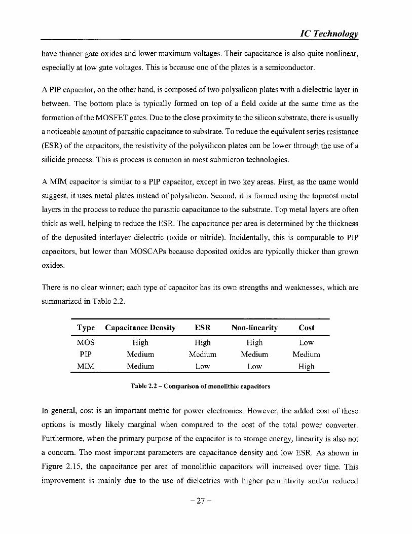
IC Technology
have thinner gate oxides and lower maximum voltages. Their capacitance is also quite nonlinear,
especially at low gate voltages. This is because one of the plates is a semiconductor.
A PIP capacitor, on the other hand, is composed of two polysilicon plates with a dielectric layer in
between. The bottom plate is typically formed on top of a field oxide at the same time as the
formation of the MOSFET gates. Due to the close proximity to the silicon substrate, there is usually
a noticeable amount of parasitic capacitance to substrate. To reduce the equivalent series resistance
(ESR) of the capacitors, the resistivity of the polysilicon plates can be lower through the use of a
silicide process. This is process is common in most submicron technologies.
A MIM capacitor is similar to a PIP capacitor, except in two key areas. First, as the name would
suggest, it uses metal plates instead of polysilicon. Second, it is formed using the topmost metal
layers in the process to reduce the parasitic capacitance to the substrate. Top metal layers are often
thick as well, helping to reduce the ESR. The capacitance per area is determined by the thickness
of the deposited interlayer dielectric (oxide or nitride). Incidentally, this is comparable to PIP
capacitors, but lower than MOSCAPs because deposited oxides are typically thicker than grown
oxides.
There is no clear winner; each type of capacitor has its own strengths and weaknesses, which are
summarized in Table 2.2.
Type Capacitance Density ESR Non-linearity Cost
MOS High High High Low
PIP Medium Medium Medium Medium
MIM Medium Low Low High
Table 2.2 - Comparison of monolithic capacitors
In general, cost is an important metric for power electronics. However, the added cost of these
options is mostly likely marginal when compared to the cost of the total power converter.
Furthermore, when the primary purpose of the capacitor is to storage energy, linearity is also not
a concern. The most important parameters are capacitance density and low ESR. As shown in
Figure 2.15, the capacitance per area of monolithic capacitors will increased over time. This
improvement is mainly due to the use of dielectrics with higher permittivity and/or reduced
-27 -

IC Technology
thickness. It is worth noting that the MIM capacitors do not include stacking and the MOS
capacitors have a thick gate oxide.
Unfortunately, at present time, the energy storage density of monolithic capacitors is inadequate
for high-performance dc-dc power converter. The major stumbling block is their capacitance per
area. For example, a thin gate oxide MOS capacitor in an 180 nm CMOS process has a density of
8.1 nF/MM2. In comparison, a 0402 MLCC from Samsung (CL05A106MP5NUNC) has a density
of 16000 nF/mm 2, if we assume the capacitance is de-rated by 35% at 2.0 V, resulting in a at least
three orders of magnitude difference in capacitor density.
16
14
a 12
10
+*MOS
-- MIM
6
2
0
Year
Figure 2.15 - Monolithic capacitor density projected by the ITRS 2012
However, there is hope, and it comes from an unlikely place. For years, the memory industry has
been using capacitors to store information in dynamic random access memory (DRAM). In order
to keep up with the unrelenting demand for larger DRAM modules, they have continually
developed a specific type of capacitor technology that uses the third dimension [76]. They are
called either trench capacitors or stacked capacitors, depending upon whether they dig into the
silicon substrate or build on top of the silicon substrate. It would go a long way, if this capacitor
technology were optimized to store energy instead of information. Recently, a multi-layer trench
capacitor with a density of 440 nF/mm2 has been demonstrated [59]. If progress continues, then
-28-

IC Technology
one day, we might see the energy storage capacitors integrated with the rest of the power
electronics.
2.4.2 Monolithic Inductors
Inductors are a very different beast from capacitors. In an IC process, a monolithic inductor is
simply a coil of wire in one or more layers of metal. The most common type of inductor is a spiral
inductor and as its name would suggest, it is a metal trace snaked around in the form of a spiral.
(a) Conventional spiral (b) Equal loop area spiral
(c) Inter-wound spiral (d) Twin spiral
Figure 2.16 - Different spiral inductor layouts
A conventional layout of a spiral inductor is shown in Figure 2.16a. In this layout, the trace
terminates in the center of the spiral and is brought out using a second level of metal. A few other
popular spiral inductor layouts are show in Figure 2.16. All of these coils are rectangular, but they
can be octagonal, polygonal, or circular. It is also possible to create solenoidal or toroidal
inductors. Even transformers can be realized: this is accomplished by stacking two spiral inductors
on top of each other.
Unfortunately, the integration of high-performance spiral inductors is a very challenging task. It is
very difficult to produce monolithic inductors with high quality (Q) factors. Depending upon the
- 29 -

IC Technology
frequency, a good spiral inductor will typically have a Q in the 10 to 30 range. To further
complicate the issue, very few silicon processes even offer support for inductors. However, III-V
semiconductor processes and silicon process geared toward RF provide pretty good inductor
models.
The main two loss mechanisms in a spiral inductor, which directly impact the Q, are ohmic loss
and eddy current loss. The ohmic losses can be reduced by forming the inductor on the topmost
metal layer to take advantage of the thick top-metal. This has the added benefit of reducing the
eddy current losses by increasing the distance to the substrate [20]. To further reduce eddy current
losses, a low-doped high resistivity substrate is used along with either a guard plane or deep trench
isolation under the inductor [19]. Figure 2.17 - Figure 2.18 show an illustrative example of a spiral
inductor in a 180 RF CMOS process from IBM.
Figure 2.17 - Isometric view of a spiral inductor with octagonal coil
Figure 2.18 - Side view of a spiral inductor with octagonal coil
This particular inductor is composed of two thick metal layers stacked on top of each other with a
trace width of 25 ptm. The first layer is 3.0 pm of copper, the second layer is 4.0 pim of aluminum,
-30-

IC Technology
and the metal via connecting the two layers is 4.0 pm of copper, resulting in a trace that has a sheet
resistance of approximately 2.0 mQ per square. The spiral inductor has an outer diameter of
290 pm and 3.5 turns resulting in an inductance of 2.14 nH with an equivalent series resistance of
201 mQ. In addition, a patterned metal ground plane is used under the inductor to terminate its
electric field. This feature reduces the capacitive substrate losses and boosts the Q factor.
Regrettably, the electrical performance of the state-of-the-art monolithic inductor technology is
not adequate for high-performance dc-dc power converters. The dc resistance per inductance is
simply too high to make an efficient power converter. The inductor we previously discussed had
a dc resistance of 201 mQ. In contrast, a 1.9 nH chip inductor from Coilcraft (0403HQ-lN9XJLU)
has a maximum dc resistance of 12 mK2. There is a gap of more than one order of magnitude
between these dc resistances and this gap will grow larger at higher inductance values.
The prospect of monolithic inductors for use in power converters is probably a little while off.
There is only a certain amount of perfornance to be gained by using thicker metal and distancing
the inductor from the substrate. To see large improvements, magnetic material needs to be
introduced into the IC process flow. Some groups have tried to enhance the basic spiral inductor
by adding magnetic material on top of the coil as well as below the coil [30]. While others have
created inductors using solenoids wrapped around a ferromagnetic core [121]. One of the more
radical solutions is the thin-film V-groove inductor [86]. In this design, a one-turn inductor is
formed by surrounding a triangular wire with magnetic material. With the continued push to
integrate more functionally into a given IC, it is only a matter of time before we see inductors
integrated with the rest of the power electronics. The only question is when?
-31 -

Chapter 3 - Power Converters
Virtually any type of consumer electronic or high-end device will typically incorporate at least one
dc-dc converter to provide the necessary dc voltages for the various integrated circuits in the
device. A dc-dc converter transfers energy stored at one voltage to an application-specific voltage.
In doing so, it provides both a voltage transformation function and an output voltage regulation
function. The goal of this thesis is to create a power converter architecture that combines the
strengths of various dc-dc converter topologies in an advantageous way. There are numerous
categories of dc-dc converters and each type of power converter excels in certain instances. In this
chapter, we discuss in detail a few of the most relevant power converter topologies for the
prototype demonstration vehicle. Consequently, we only discuss step-down power converters in
this chapter.
3.1 Switch-Mode Converters
Over the years, there has been a considerable amount of work in developing switch-mode dc-dc
converters and nowadays they are ubiquitous. They are arguably the oldest type of efficient power
converter. By definition, switch-mode converters switch between two or more states and the
transistors act as switches, which ideally do not dissipate power. This is in contrast to linear
regulators, which have a single state and the transistors are continually dissipating power. In this
thesis, we assume that switch-mode converters utilize both inductive and capacitive storage
elements. Consequently, switched capacitor and switched inductor power converters do not belong
within this category. Switch-mode converters are a broad category of power converters that include
Buck converters, fly-back converters, full bridge converters, forward converters, and so on.
3.1.1 Buck Converters
One of the most basic switch-mode converters is the Buck converter. Its origins can be traced back
to the middle of the 2 0 th century with the advent of the transistor. It is commonly used to supply
power to logic devices such as microprocessors. Figure 3.1 illustrates a Buck converter that
consists of three main components: a high-side switch SH, a low-side switch SL, and an LC filter.
Both SH and SL can be implemented using transistors (e.g., MOSFETs or BJTs) while SL can be
-32-

Power Converters
implemented using a diode. It is worth noting that when SL is implemented using a switch, it is
called a synchronous rectifier.
SH Vm2 L
Vin+ L L cC
Figure 3.1 - Simplified schematic of a Buck converter
Figure 3.2 illustrates the operation of the Buck converter, where SL and SH are always in
complementary states. In the first state, SL is open and SH is closed, whereas in the second state, SL
is closed and SH is open. The Buck converter will cycle back and forth between these two states at
a given switching frequency fs This produces a rectangular pulse train Vm2 with a peak voltage
equal to the input voltage Vi,,. By passing Vm2 through the LC filter, a dc output voltage VO is
generated. Care must be taken to prevent both switches from being on at the same time; otherwise,
there will be a power-to-ground short.
4'
Vm2
ton
XL, 2AiL,2
Figure 3.2 - Midpoint voltage and inductor current waveforms in a Buck converter
-33-
VO0

Power Converters
The magnitude of Vvtan be controlled by selecting the proper on-time t0nof the upper switch
because Vo is the average of Vm2. Clearly, the longer SH is on, the larger the magnitude of Vo. It then
follows that
V, = DV, (3.1)
where the duty cycle is defined as
tD =f In (3.2)T
In the steady state, the inductor L is the sole source of output current Io through the load, thus
iL ='2 (3.3)
The inductor current ripple can be determined by
AiL 2 = " 0 .LIDD (3.4)fswL
Furthermore, by substituting eqn. (3.1) into eqn. (3.4), AiL,2 can also be found using
AiL2 = . (3.5)
Because Vm2 is fed into a second order filter, the output voltage ripple is given by
Av0 2 - AiL2 -,D (3.6)8fWC 8f ,LC
(Please note: the ESR of the capacitor is neglected in the above calculation.)
Based upon the work of Wolaver, Figure 3.3 illustrates the transfer of dc power and ac power in a
Buck converter [116]. The ac-active set includes SH, while the dc-active set includes SL. In this
sample example, the Buck converter has an input voltage of 5.0 V, an output voltage of 1.0 V, and
a load current of 1.0 A. During the dc-ac-dc conversion process, 0.8 W of dc power delivered from
the input is absorbed by SH where it is converted into 0.8 W of ac power. Next, 0.8 W of ac power
delivered from Sr is absorbed by SL where it is converted into 0.8 W of dc power and delivered to
-34-

Power Converters
the load. Assuming the load absorbs 100% of the power, then 80% of the power comes from a dc-
ac-dc conversion process and 20% of the power comes directly from the input.
\ Pd=0.8W
Vm2 Lr 0- _
SH -- - +Pdc=0.8W
5V~ SL C IV
/ Pa=0.8W
Pd =0.2W
Figure 3.3 - Power transfer in a 5.0 V to 1.0 V Buck converter
In general, the amount of inverted power for a Buck converter is given by
(3.7)PIC = (10 " P, .
This relation is true for all variants of the Buck converter that are further discussed.
The equation above illustrates the fact that, as the step-down ratio increases, the amount of power
needed to be inverted also increases. Therefore, with all else being equal, a Buck converter with a
large step-down ratio will be less efficient than a Buck converter with a small step-down ratio.
We now explore how the achievable switching frequency of dc-dc converters in deep submicron
CMOS processes scales with process voltage. For simplicity, we focus on CMOS synchronous
Buck converters.
Now consider how this device-scaling characteristic influences converter performance. As shown
in Schrom et al. [93], the MOSFET losses in a synchronous Buck converter can be modeled using
an effective bridge capacitance Cb and an effective bridge resistance Rb, as illustrated in Figure
3.4, where WL, WH, CLO, CHO, RLO, RHO are the widths, effective specific capacitances, and specific
-35-

Power Converters
on-resistances of the switches. Typically, the gate capacitance is the dominant contributor to
dynamic loss in low-voltage CMOS processes. Therefore, this model ignores commutation loss.
Rb
-0 SH -0
I0+
in + b SL R VO
Figure 3.4 - Buck converter model for calculating energy losses
In this model, we have defined the following parameters as
Cb =WLCLO [WHCHO (3.8)
and
Rb= RLO D mID[L RHOD (3.9)WL WH
The optimal width ratio of WH to WL can be found by a constrained minimization of Cb at a constant
Rb, yielding
WH _ DRHOCLO- - )R . [93] (3.10)a=WL 1 D)RL0 HO
Assuming that the power loss is only in the MOSFETs, then the total power loss is a combination
of the static loss and dynamic loss given by
loss = Cb , L RbJ =WCO "ns, [ R (3.11)W
where
-36-

CCbW
CLO L aCHO
11a
and
RO=RW=[IEaf1I D ERLEDRHO
The optimal Cb can be found by minimizing P0 ss (eqn. (3.11)), yielding
I R, 0OVtr FCbO f,
which results in a minimum power loss of
(ss )nn> = 2W,,op CbOfs = 210K I.4RoCofw.
An optimalfs, can be chosen given a desired Ploss (min) or, equivalently, a desired efficiency. This
optimum is
opt nRloss (m C)
Pt412 V 2 Ro, bn CbO h
(3.16)
Additionally, by combining eqns. (3.2), (3.10), (3.12), (3.13), and (3.16), holding Io and Ploss (min)
constant, and assuming RHOCHO a Vn and RLOCLO a Vi (in line with eqn. (2.13)), it can be shown
that the optimalfs, is
where
Vik7 1 V7 11 V~bC E FG 7F
V b7= V,0 L V, ,
(3.17)
(3.18)
and
b =RNOCNO (3.19)
-37-
Power Converters
(3.12)
(3.13)
(3.14)
(3.15)

Power Converters
In equation (3.19), b represents a relative performance factor for SH and SL. If both devices exhibit
the same RC product (e.g., are both NMOS), then b equals one. More typically, SH is a PMOS and
SL is a NMOS, so b is closer to three. Furthermore, it can be shown empirically that f0 Pt fits the
power law
= kf ,O (3.20)
assuming both / and k are functions of b and V0, and given Vin > 2 V. Figure 3.5 shows how the
exponent f varies as a function of b for various V.
-2.50 -
-2.55 - -VO = .0v
-2.60 - -Vo = 1.2V-Vo = 1.5V
-2.65
, -2.70
-2.75
r -2.80-
-2.85 Increasing Vo
-2.90
-2.95
-3.001.0 1.5 2.0 2.5 3.0 3.5 4.0
Performance Factor (b)
Figure 3.5 - Exponent P vs. relative performance factor (b)
What can be concluded from eqn. (3.20) and Figure 3.5 is that fpt increases very rapidly with
decreasing Vi,. For example, if b = 3 and V = 1.0 V, then / = -2.67. Therefore, a Buck converter
with a Vin of 1.8 V should be able to switch 15.3 times faster than a Buck converter with a Vin of
5.0 V with equal power loss in both cases. This leads to less energy storage in the filter elements
(L and C) for a given dynamic and static response.
While this analysis, which was first presented in a publication by the author [84], does not include
all salient loss mechanisms, it nevertheless points to the dramatic frequency capabilities of low-
voltage CMOS processes. These capabilities are increasingly reflected in the literature. Recently,
-38-

Power Converters
several high frequency (> 100 MHz) low-voltage dc-dc converters have been demonstrated in deep
sub-micron CMOS [49, 94, 93, 114]. The switching frequencies of these converters are roughly
one to two orders of magnitude higher than commercial products. This can be attributed to their
use of deep sub-micron CMOS. For our purposes, we can conclude that separating a design into
two stages as proposed in Chapter 5 has substantial potential advantages owing to the described
scaling characteristics of CMOS.
3.1.2 Multi-Level Buck Converters
The traditional Buck converter previously discussed converts power by chopping the input voltage
Vi and then averaging this voltage using a LC filter. The chopped waveform Vm2 has a maximum
voltage of Vi, and a minimum voltage of 0 V. Thus, this power converter has two distinct levels.
However, it is possible to extend a Buck converter to multiple levels using additional components
and this extension is the subject of this section. From now on, we will refer to the traditional Buck
converter as a two-level Buck converter.
Any Buck converter with more than two levels is considered a multi-level Buck converter and two
such converters are shown in Figure 3.6 and Figure 3.7. Initially, we discuss the specific three-
level Buck converter shown in Figure 3.7. We then extend this topology to n levels to explore the
advantages and challenges of increasing the number of levels.
Vm3 L3
Cf /1I(P3+
Vin G C3~~ R V,
Cf Td __ee r- Bk_ t
Figure 3.6 - Diode clamped derived three-level Buck converter schematic
-39-

Power Converters
Figure 3.7 illustrates a three-level flying capacitor Buck converter [72]. This is a popular multi-
level converter because it only requires two additional switches and one additional capacitor to
create an extra level, which is equal to V/2.
Vm3 L
Cf O4+
Vin C3T R Vo
Figure 3.7 - Three-level flying capacitor Buck converter schematic
In the three-level flying capacitor Buck converter, there are a total of four switches controlled by
the following gate signals pi, P2, y3, and p4. The main switching FETs are controlled by (pi and q3
while q2 and (P4 serve as the gates signals for the synchronous rectifiers. The gate signals (pi and p2
are complementary and similarly the gate signals q3 and (P4 are also complementary. It is worth
noting that pi and (3 have the same duty cycle D and are phase shifted by 180' under steady state.
A portion of the gate signals and switch node voltage Vm3 are shown in Figure 3.8 when D < 1/2 and
in Figure 3.9 when D > V. For simplicity, q2 and (P4 are not shown because they are complements
of qpi and (P3.
4 (1-D )x Ts, F __ _
Vm3 1 1
Figure 3.8 - Node voltages in a three-level Buck converter when D < %
-40 -

Power Converters
01Dx Tsw
(
t
Vm3
1 2 3fsw fsw fsw
Figure 3.9 - Node voltages in a three-level Buck converter when D > %/
Figure 3.10 shows the four possible switch configurations for this power converter based upon the
gate signals shown above. When D < %, the switches cycle through modes 1, 3, 1, 4 and when
D > 1/2 the switches cycle through modes 2, 3, 2, 4.
T TSI
S2_L -VM vV
S 3
Mode 2 Mode 3 Mode 4V.3=Vi. v.3=Vi. 2 v. 3=Vin 2
S4
(a) Mode 1 (b) Mode 2 (c) Mode 3 (d) Mode 4
Figure 3.10 - Four possible switch configurations in a three-level Buck converter
It is important that the power converter always alternate between mode 3 and mode 4 regardless
of D so that the flying capacitor Cf will have a voltage v, that is equal to Vin/2. It can be argued
that v, is naturally balanced as long as D is equal for pi and P3. However, this constraint is difficult
-41-

Power Converters
if not impossible to meet in real applications. For example, if there is any type of load transient
then, vC will tend to go to one of the voltage rails. Therefore, active control of Cf is often required
to balance vc.
If we assume vc is equal to V/2, then Vm3 can be one of three possible levels: 0, V/2, or Vn. Under
steady-state operation, Vm3 is a pulsating waveform with a frequency of 2xfsw. Its minimum and
maximum voltage levels are 0 and Vin/2 for D < % while Vi/2 and V for D > 1. The output
voltage is the average of V,3, which is equal to Vi multiplied by D. The three-level operation
effectively doublesfs, and lowers the peak voltages Of V.3, resulting in a favorable tradeoff in filter
size and converter efficiency.
In the three-level Buck converter, the peak-to-peak inductor current ripple can be determined using
AiL, 3 n -1D D for0<D< 2 , (3.21)
and
AiL3 V 3 E VD DV-I for 2<D<1 (3.22),fL 3
It should be noted that the maximum AiL,3 occurs when D equals 1/4 or 3/4.
Additionally, in the three-level Buck converter, the V, ripple can be calculated by
AvA,3 = x - - (3.23)8C3fs, 2
If we substitute eqn. (3.21) into eqn. (3.23), we obtain
Avo,3 X --w D D for 0<D<' . (3.24)8f 2L3 C3 2 2 (.4
Similarly, if we substitute eqn. (3.22) into eqn. (3.23), we obtain
__ 11Avv 3 = x-JLD DE-I for 2<D<1 - (3.25)' 8 fL 3C32 2
-42-

Power Converters
It is instructive to compare the three-level Buck converter to a conventional two-level Buck
converter. For example, if the LC filter andfs, of the three-level Buck converter are the same as a
two-level Buck converter, then the maximum V ripple is reduced by a factor of eight.
Conversely, if the maximum V ripple of the three-level Buck converter and the two-level Buck
converter are held constant (i.e., max(Avo,3)=max(Avo, 2)), then either the LC filter and/orfsw of the
three-level Buck converter can be reduced. The amount of reduction in filter inductance L3 is a
function of D and subsequently V0. We have plotted the ratio L3/L2 of for a three-level Buck
converter is illustrated in Figure 3.11, where AiL, Vin, andfsv are held constant. There is at least a
twofold reduction in L3 and, when D is equal to V, L3 equals zero. Unfortunately, power converters
typically need to be able to operate over a range of input and output voltages, so it is not practical
to run the three-level Buck converter when D is equal to 50% all the time. Nevertheless, there is
at least a twofold reduction in inductance and perhaps more if the power converter is run over a
narrow Vin, range and/or a narrow V range.
0.50
0.45
0.40
0.35
0.30
0.25 Vin=1.6V
0.15 --- Vin=1.7V0 .2 0 - - -- V n 1 9
0.05 -- - -- Vin=2.7V
0.15
0.10
0.000.0 0.5 1.0 1.5 2.0
Output Voltage (V)
Figure 3.11 - Inductance reduction for three-level Buck converters
The number of levels in a flying capacitor Buck converter increases as the number of switches and
capacitors increase. For example, a four-level flying capacitor Buck converter requires four
additional switches and two additional capacitors to create two extra levels (1/3 V, and 2/3 V), as
depicted in Figure 3.12. Similarly, a five-level flying capacitor Buck converter requires six
additional switches and three additional capacitors to create three extra levels (1/4 Vin, 2/4 Vi, and
-43 -

Power Converters
3/4Vi), as depicted in Figure 3.13. In general, two extra switches and one extra capacitor are
required for each additional level in a flying capacitor Buck converter.
vi,
02 M2
4 M4 r C4 R
06- M
Figure 3.12 - Four-level flying capacitor Buckconverter schematic
V;,.
A
Ml2
#6J MR0'- M,
Figure 3.13 - Five-level flying capacitor Buckconverter schematic
During steady-state operation, each switch is only exposed to the average dc voltage on the flying
capacitors so low-voltage devices can be used. For example, the maximum required blocking
voltage for a switch in a three-level Buck converter is 1/2 Vi, whereas, in a five-level Buck
converter it is 1/4 Vi. Similar to the case of the three-level converter, the four-level operation
effectively triples fs, while the five-level operation effectively quadruples fs. In general, for an
n-level Buck converter, the required blocking voltage for the switch is Vin divided by n - 1 and theeffectivefs, is multiplied by n - 1.
Similar to the three-level Buck converter, the peak voltages at V.4 and Vm5 result in a favorable
tradeoff in filter size and converter efficiency. In general, the inductor current ripple in an n-level
Buck converter can be determined using
AiLn I ' O D D for 0 < D < 1/(n-1)f,,n 0 1 (3.26)
Additionally, the V, ripple in an n-level Buck converter is
-44 -

Power Converters
Ai 1Av ,= AiL,n X8Cnfs n
(3.27)
By substituting eqn. (3.26) into eqn. (3.27), we obtain
Av = '" x 1 - EDD for 0 < D < 1/(n-1)""8f2LnC n n nE1
(3.28)
The ripple currents and voltages calculated in eqn. (3.26) and eqn. (3.28) are only correct when
D > 0 and D < 1/(n-1). However, there are corresponding equations for the remaining portion of
the D range. In Figure 3.14a, the normalized inductor current ripple is plotted over the complete
D range for Buck converters with various numbers of levels. Likewise, Figure 3.14b illustrates the
normalized V ripple over the complete D range [46]. To aid in visual comparison between the
different power converters, the ripple values were normalized to one.
1.0-2-Level
0.8-3-Level-4-Level
0.6
0.4
0.2
0.00.0 0.2 0.4 0.6 0.8 1.0
Duty Cycle (D)
(a)
1.0-2-Level
-3-Level0.8 -4-Level
0.6
0.4
0.2
0.00.0 0.2 0.4 0.6 0.8 1.0
Duty Cycle (D)
(b)
Figure 3.14 - Normalized current and voltage ripple for n-level Buck converters
The graphs have a similar shape because Av0 ,n is a scaled function of AiLn as shown in eqn. (3.27).
In the three-level Buck converter, there is only one value of D at which there is zero current ripple
and zero voltage ripple, whereas, in the four-level Buck converter, there are two distinct values. In
general, an n-level Buck converter has (n-1) zero-ripple values.
We have chosen to create ripple cancellation factors to assist the comparison. In the case of the
inductor ripple current, we have defined the ripple current cancellation factor as
-45 -
V-
Z

Power Converters
AikiL = Ln
AiL,2(3.29)
We can also defined the ripple voltage cancellation factor as
Aikic = _cn
AC,2(3.30)
Both of these ripple cancellation factors are just another way of looking at the improvement in
ripple characteristics when adding multiple levels. To help visualize this enhancement, we have
plotted kii versus D in Figure 3.15a and k,0 versus D in Figure 3.15b.
3-Level
-4-Level
0 0.2 0.4 0.6 0.8 1Duty Cycle (D)
0.25
0.20
0.15
0.10
0.05
0.000..0
3-Level
-4-Level
0 0.2 0.4 0.6 0.8 1Duty Cycle (D)
(a) (b)
Figure 3.15 - Ripple reduction for n-level Buck converters
With all else being equal, utilizing a multi-level converter reduces the output filter requirements.
For example, by holding Aimax andfs, constant, the output filter for an n-level Buck converter can
be reduced by
L 1 C ___" = with C 1
L2 l 1 L C2 Lh E 1(3.31)
Furthermore, assuming Ln,fsv and Avo,max are held constant then C for an n-level Buck
converter can be reduced by a factor
Cn 1
C 2 ELh wI(3.32)
-46-
0
0.50
0.45
0.40
0.35
0.30
0.25
0.20
0.15
0.10
0.05
0.000. .0

Power Converters
The reduction in filter inductance and/or filter capacitance increases considerably with a greater
number of levels and is one of the main motivations for increasing the number of levels.
Unfortunately, balancing the flying capacitor becomes progressively more difficult as the number
of levels increases, so multi-level converters with more than three levels are quite rare.
3.1.3 Multi-Phase Buck Converters
Analogous to a multi-level Buck converter, a multi-phase Buck converter (or interleaved Buck
converter) places n Buck converters in parallel between the input and load to achieve improved
performance. Figure 3.16 shows a multi-phase Buck converter where each "phase" is a Buck
converter. The first phase consists of a low-side switch SL1, a high-side switch SH1, and a filter
inductor L,1, whereas the nth phase consists of a low-side switch SLn, a high-side switch SHn, and a
filter inductor Lpn. All of the phases share a common output capacitor C, but each phase is shifted
by 360/n degrees with respect to each other.
SHI L 1
SuSL
4iL
T ~ Sin i(Pn
Figure 3.16 - n-phase interleaved Buck converter schematic
Theoretically, an n-phase Buck converter is able to respond to load changes as if it were switched
n times faster than a single-phase Buck converter without actually switching at a higher frequency.
Unfortunately, an improvement of n in response time (i.e., control bandwidth) only occurs with
perfectly matched phases.
In contrast to a single-phase design, a multi-phase converter has a reduced V, ripple with the same
C. This is best explained through an example. Let us assume a two-phase design where the first
-47 -

Power Converters
phase is shifted by 1800 with respect to the second phase and the inductor current of each phase is
saw-tooth when D is equal to 25%. The effective inductor current iL is the summation of the
inductor current of each phase ii - i.2. As can be seen in Figure 3.17, iL will have a peak-to-peak
current ripple that is 65% of the original ripple and twice the frequency. In this example, the
smaller ripple current of iL results in either a smaller V ripple or a smaller C when compared to an
equivalent single-phase design.
" D=25%
I IV2
A
LIZ~
0.5xTswi,+ i,2
0.6 5 (IA)
t _ _t
Figure 3.17 - Addition of two saw-tooth waveforms with duty cycles of 25% and phase shift of 180'
Interestingly, if D is 50%, then iL will be a pure dc current.
multiple inductor currents will completely cancel out and,
thereby reducing the V, ripple.
0.60 T-
0
0
cJ
0.50
0.40
0.30
0.20
0.10
N
K11
0.00 t-0.0
Therefore, under certain conditions,
in other cases, partially cancel out,
-n=2
-n=3
-n=4
-n=5
-n=6
7
/ / /7
0.2 0.4 0.6 0.8 1.0Duty Cycle (D)
Figure 3.18 - Capacitor ripple current cancellation factor (kic) as a function of duty cycle
-48 -
z

Power Converters
As depicted in Figure 3.18, the amount of ripple voltage cancellation of a multi-phase converter
depends upon the number of phases and D. The definition of the ripple voltage cancellation kic
factor is given by eqn. (3.30). As the number of phases increases, the ripple cancellation effect
improves. The total number of points where complete ripple cancellation occurs is n-i. The
frequency of the resulting current ripple is also multiplied by n.
The equivalent inductance Leq of the parallel combination of the filter inductors for each phase is
LLeq = LI, (3.33)
n
where L, is the inductance of a single phase. An n-phase converter gives n-I zero-ripple points at
the following duty cycles:
Do =M/n where m=1,2, ... n-1. (3.34)
The multi-phase V, ripple can be calculated by
k. V [I E DEAv,2 = , (3.35)8f2 LqC
while neglecting the ESR of C.
Similarly, it is also possible to reduce the ripple current in the inductors using multiple phases if
the inductors are coupled [118, 65]. For example, let us assume a two-phase design with positively
coupled inductors. When SHi and SL2 are turned on, the current through L, 1 increases thereby lifting
up the decreasing current through L, 2. Alternatively, when SL1 and S 2 are turned on, the current
through L 1 decreases thereby pulling down the increasing current through L ,2 . Figure 3.19 depicts
the amount of ripple current cancellation in a two-phase Buck converter with various coupling
factors k. For reference, the ripple current cancellation kiL factor is defined in eqn. (3.31).
As can be seen from Figure 3.19, ripple cancellation improves (i.e., kiL increases) with increasing
coupling factors and as D approaches 50%. Unfortunately, as D moves towards 0% or 100%, the
introduction of a coupling factor k increases the ripple current. This occurs because there is a
noticeable amount of time at which the current in both inductors are increasing or decreasing at
the same time so the positive coupling enhances the ripple. If the coupling were negative, then the
-49 -

Power Converters
opposite would happens: there would be enhancement of the ripple current at D of 50% and
reduction of the ripple current at the extreme D range.
1.20
1.15 -- k=0.05--- =. 10
I .10 -- - k=u. 15 1-=0.20
1.05 -- k=0.25-k=-0.30
1.00 -- =0.35
0.95
0.90
0.85 -
0.80 -
0.75 -
0.700.0 0.2 0.4 0.6 0.8 1.0
Duty Cycle (D)
Figure 3.19 - Inductor ripple current cancellation factor (kiL) as a function of duty cycle
It is common to improve performance of a single-phase Buck converter design by changing it into
a multi-phase design. However, the number of inductors and MOSFETs will increase, control
becomes more difficult, and inductor matching is more critical. Therefore, it is uncommon to see
any benefit with designs that have more than eight phases.
3.2 Switched Capacitor Converters
A switched capacitor (SC) converter consists of a network of active devices and capacitors. They
only utilize capacitors as their source of energy storage. Energy is transfer from the input to the
output by cycling the SC network through different topological states. If the SC converter is a dc-
dc power converter, it must contain at least one switch while the remaining active devices can be
diodes. For improved performance, especially at low-voltage operation, the diodes can be replaced
by switches at the added cost of complexity.
To whet the appetite, we briefly discuss a series-parallel SC converter. This type of SC converter
is the probably the simplest and easiest to understand. During the first phase of operation, the
capacitors are stacked in series, whereas in the second phase of operation, the capacitors are
-50-

Power Converters
stacked in parallel. Figure 3.20 shows both the charge and discharge phases of a 2:1 series-parallel
SC converter.
S1 S3 S1 S3
Qn Q03 0 + QU4VC1 C c1vcI C1
Vin VO 'U
S4 S4
S2 S2
(a) Charge phase (b) Discharge phase
Figure 3.20 - 2:1 series-parallel SC converter schematic
In operation, this SC converter will cycle back and forth between these phases at a given switching
frequencyfs, thereby converting an input voltage Vin to an output voltage V. During the charge
phase, the capacitor voltage vci and V, must add up to V, whereas in the discharge phase, vc and
V0 must be equal to V.' Consequently, V is equal to Vin/2. Even more fundamentally, the charge
transfer requirements on the capacitor for periodic steady-state operation imposes a 2:1 ratio of
average output current to average input current. In this instance, the load is a constant voltage
source. However, the circuit would operate equivalently if the V, source were replaced by a large
capacitor and load resistor.
The above example is just one type of SC converters. There is a limitless number of SC networks
that can provide a specific voltage transformation. Unfortunately, a vast majority are impractical.
It is desirable for a SC network to have a common ground, large conversion ratio, low switch
stress, low dc capacitor voltage, low output resistance, and so forth. Bounds on the minimum
number of capacitors and switches possible to achieve various conversion ratios have been
developed [68]. However, over the years a few SC topologies stand out, chief among them Ladder,
Dickson, Series-Parallel, Fibonacci, and Doubler. We briefly cover the operation of each of these
five SC topologies after we first discuss the fundamental loss mechanisms in all switched capacitor
converters.
-51 -

Power Converters
3.2.1 Switched Capacitor Loss Mechanisms
To help understand the loss mechanisms in SC converters, it is instructive to first analyze the
classical capacitor charging problem, as depicted in Figure 3.21. The capacitor C is initially
charged to some value v, (0) and at t = 0 the switch is closed. At that instant, a brief surge of current
will flow into the capacitor C as it charges to Vi,,. The charging rate is typically described in terms
of a time constant T=RC, which is the time it takes the voltage on the capacitor to either rise or fall
to within 1/e of its final value.
S R
t=O
Vin + C -NVC
Figure 3.21 - Charging of a capacitor with a series resistance
The voltage vc (t) across the capacitor is given by
v (t) =v(0)D [,. E vC(0)] ij L e tIRCE. (3.36)
While the current ic (t) flowing through the capacitor is
.d v K~LIv~(O LItIRCi (t)= C = " v (0) e (3.37)
dt R
The energy loss Elss (t) charging the capacitor can be found by calculating the energy dissipated
in resistor R, which is given by
ElOs (t)= iR (xR (t) dt =f [i,(t)]2 R dt . (3.38)
When we substitute the expression ic (t) from eqn. (3.37) into eqn. (3.38) and solve the integral
then E,0 s(t) simplifies to
- 52 -

Power Converters
Eos (t) V,, 0v,(0)]' C[11eOt/RC (339)
If the transients are allowed to settle (i.e., t->oo), the total energy loss charging the capacitor is
independent of its resistance value R. In this case, the amount of energy loss is equal to
1E1 (oo)= - CAc . (3.40)
2
A SC converter can be modeled as an ideal transformer with a fixed Ni:N2 conversion ratio
followed by a finite output resistance Ro (assuming Rin is absent). A dc model is shown in Figure
3.22, where Ro accounts for the power loss in the charging/discharging the energy transfer
capacitors. This power loss is typically dissipated in the on-resistance of the MOSFETs and ESR
of the capacitors.
An intuitive basis for this model is as follows: the switched capacitor topology imposes a fixed
current conversion ratio from input to output that is fixed by the requirements of maintaining
capacitor charge balance in periodic steady-state operation. The transformer reflects this current
conversion ratio. The output resistance captures the fact that the voltage conversion ratio does not
necessarily follow the ideal case of the inverse of the current conversion ratio, with differences in
the actual to ideal conversion ratio directly reflected in the internal charging and discharging loss
of the capacitors.
Iin Rin N 1 : N 2 Ro I0
Vin VO R
SC Converter
Figure 3.22 - DC model of a switched capacitor dc-dc converter
In the dc model of a SC converter, the output voltage is given by
- 53 -

Power Converters
N, = ,2 0 IOR, , (3.41)
where Io is the dc output current.
Instead of accounting for the power loss using Ro, it is possible to use an input resistance Rin. When
Ro is present in Figure 3.22, Rin should be absent, and vice versa. The relationship between the two
resistances is given by
(3.42)
Reflecting Ro to the input can sometimes be useful. If Ro is known for a step-down converter, then,
when run backwards, Rin becomes Ro. For example, if a 3:1 step-down SC converter with a Ro of
1.0 n is run backwards, it becomes a 1:3 step-up SC converter with a Ro of 1/9 Q.
Calculating Ro is a bit involved since it is a complicated function of many variables such as:
parasitic resistance, switching frequency, and so forth. In Figure 3.23, Ro is plotted versusfs, for a
2.0 W SC converter. Fortunately, there are two limiting cases where the operation of the SC
converters can be simplified and Ro easily found.
0.3
I
0.031.0E+05
---- RSSL
---- RFSL
---- RO,APPOX
-RO,SIM
I *~..
1.OE+06 1.OE+07 1.OE+08Frequency (Hz)
Figure 3.23 - Representative SC output resistance vs. frequency
- 54-
------------------
Rin = R (2 N,

Power Converters
The first limiting case is when the switching period T, (1/fs") is much longer than the RC time
constant T of the energy transfer capacitors. Under this condition, a fixed amount of energy is lost
(1/2CxAVc 2) that is irrespective of the resistance of the capacitors and switches as previously
derived. The converter is said to be operating in the slow switching limit (SSL) and R, is given by
R = RSSL c' (3.43)i jcaps j=1 2C, fs
If it is a two-phase converter (i.e., n = 2) at 50% duty cycle, then eqn. (3.43) can be simplified to
RsSL (3.44)iecaps i m
The charge multiplier ai is defined as the amount of charge through capacitor i during phase j.
Similarly, the charge multiplier vector is a' is defined as
a = [_ (3.45)qout
A set of charge multiplier vectors given by ac through a'j can be derived for any valid n-phase SC
converter [95, 96]. For the series-parallel network shown in Figure 3.20, the charge multiplier
vectors for the capacitors obtained through Kirchhoff's current law (KCL) is
a. =[1/2 1/2 D1/2]T (3.46)
and
a2 =[1/2 01/2 0]T . (347)
If the total capacitor energy Etot is fixed and the capacitors are sized optimally with respect to each
other, then the optimized output impedance R*SSL for a two-phase SC converter is
RsSL 2E I (.I: aivj[atedL (3.48)ace by caps
and the total capacitor energy is given by
- 55 -

Power Converters
Eo C e , (3.49)iEcaps2
where vc,i(rated) is the rated voltage of capacitor i. This value might be different from the actual dc
voltage on the capacitor.
In the second limiting case, u >>Tsw, the charging and discharging currents are approximately
constant, resulting in a triangular ac ripple on the capacitors. Hence, R" is sensitive to the series
resistance of the MOSFETs and capacitors, but is not a function offsw. In this case, R, of a SC
converter operating in the fast switching limit (FSL) is a function of parasitic resistance and given
by
RIT =RFSL = ni R 1 r, (3.50)iesw j=1
where Ri is the on-resistance of switch i. The charge multiplier ai is defined as the amount of
charge through switch i during phasej [95, 96]. If it is a two-phase converter (i.e., n = 2) at 50%
duty cycle, then eqn. (3.50) can be simplified to
R FSL = 2 1 R. rJ . (3.51)ieswitches
For the series-parallel network shown in Figure 3.20, the charge multiplier vectors for the switches
obtained through KCL is
a [1/2 0 0 E1/2]T (3.52)
and
a=[0 El/2 1/2 0]. (3.53)
The sign of aj, for switch i indicates the direction of current flow with respect to the blocking
voltage during the off state. Therefore, a is positive when the switch conducts positive current
while turned on and blocks positive voltage while turned off.
-56-

Power Converters
Similar to in the SSL case, an optimized output impedance R*FSL in the FSL case can also be found.
However, by holding the total switch conductance Xto0 constant, the optimal two-phase FSL output
impedance is
FSL -aIZs r,i ,i[}ated[l2 (3.54)Atotk ieswitches2
and the total switch conductance is given by
X,= ( GVi,2 ~,i~n (3.55)ieswitches
where Gi (1/Ri) is conductance of switch i.
An approximation of Ro has been proposed by Arntzen and Maksimovic [10] and is given by
R, - RFsL IE] c Lsw . (3.56)
The corner frequency (fi) is the frequency where eqn. (3.22) and eqn. (3.56) are equal and can be
rewritten as
R0 (f) ~ R'sL E RSSL (3.57)
This approximation underestimates Ro, but is usually a good starting point in the design process.
The calculations for RSSL and RFSL given in eqns. (3.43) through (3.55) are based upon the charge
multiplier vector concept outlined in Makowski and Maksimovic [68] and developed by Seeman
[95, 96]. The vector a' through a" can be obtained by inspection for any standard well posed n-
phase converter. The charge multiplier vectors are computed using the KCL constraints in each
topological state along with the steady-state constraint that the n charge multiplier quantities must
sum to zero on each capacitor. Certain assumptions are made to get closed form solutions. Chief
among them is the assumption that the output capacitor is sufficiently large such that Vo is constant.
Once Ro is known, the conduction loss can be calculated by
PCOnd = 1 2Ro . (3.58)
-57-

Power Converters
Other losses associated with the switched capacitor converter can also be calculated, such as
dynamic losses, driver losses, control losses, and so on. The dynamic losses originate from
charging and discharging the capacitive nodes and are proportional to frequency. In a well-formed
SC converter, these losses should actually be comparable to Pond.
In order to optimize the efficiency of the SC converter, the optimalfsm, capacitors, and device sizes
must be selected. Iffs, is too low, then Pcond dominates; and iffs, is too high, then the dynamic
losses dominate. Increasing fs, far above the transitional region between the SSL and FSL does
not lower R,. The primary reason to operate at such a high frequency is to reduce the V ripple at
the cost of increased dynamic losses.
0.10 - -
91-"' W/C-C decreasing % % /
SwStchin .-. fV
slow sv Fast Swi hing L mit
0.01 _ _ ._
Frequency (Hz)
Figure 3.24 - SC output resistance with varying capacitance and device width
In a well-formed design, the optimal f, is in the transitional region between the slow switching
limit and fast switching limit. This makes the design process challenging because there are no
accurate closed-form solutions for R, in this region. To complicate the process further, the optimal
fs, is a function of 1.
It is possible, however, to calculate the exact output resistance of a SC converter by solving all of
the state variables of the converter over a complete switching period. Once the state variables are
known, Ro can be found as follows:
-58-

Power Converters
RO =n N2 ", (3.59)('a) N \I'/
where N/N2 is the ideal conversion ratio. If the load is a resistor, <v0 /Io> is equal to the load
resistance. Calculating the required voltages and currents can be computationally intensive, but
done quickly using MATLAB. For example, Figure 3.25 shows a 3:1 step-down series-parallel SC
converter.
2 1
6 +
Vss
Figure 3.25 - 3:1 series-parallel SC converter schematic
The state variables for each capacitor can be obtained by solving the general transfer function
shown in eqn. (3.60) along with the differential equations describing the behavior of the capacitors
shown in eqns. (3.61) through (3.63).
FC1 a b c v j= d e f V ] k Vin (3.60)
0,_g h i -v, -1
ill = C19ei (3.61)
i 2 = C2Ac 2 (3.62)
i3 = Cv' (3.63)
The constants (a - 1) depend upon the configuration of the switches and capacitors in the network,
and therefore the charge and discharge phases have different transfer functions.
-59-

Power Converters
+ +C1 N Ve1 C2 Vc2
+ Vi . R. 6 C0 V R
0TV0
Figure 3.26 - SC charge phase (pl) for 3:1 series-parallel SC converter
R.2 R.5
+ +
C1 - Vd1 C2 Vc,2
+
____TV 0R.4 R.7
Figure 3.27 - SC discharge phase (92 ) for 3:1 series-parallel SC converter
For example, in the circuit above, constant a in charge phase is equal to
1alp -D? 1 (3.64)
elC, [)R,,1 ER,3 [' R.m6
while constant a in discharge phase is equal to
1al = C -- 1 (3.65)
C2 []mkt2 [] Rm4
Once the transfer function is known for each phase (p1 and p2 in this case), the state variables can
be computed over a full switching cycle and spliced together at the transition point. At the
beginning of each phase, the state variables are equal to the state variables at the end of the previous
phase. These boundary conditions are shown below:
- 60 -

Power Converters
(A= 0... DT,
Vd,91 (0) = v q,2 (T Ll)
(3.66)
(3.68)
(p2 = DT ... T)
v2(DT,)= iv (DTs,)
Figure 3.28 shows a fully constructed cycle for the 3:1 series-parallel SC converter. During pi,
the converter is in the charge phase (i.e., input current is finite), while during (p2 the converter is
in the discharge phase.
Now that the state variables are known over a full switching cycle, the output resistance can be
calculated using eqn. (3.59). In this specific example, R, is equal to 0.035 Q, Vi,, is equal to 5.5 V,
and R is equal to 2.0 9.
1.850
1.830
1.810
1.790
1.770
1.7500.0 0.2 0.4 0.6 0.8 1.0
Time (psec)
0.95
0.94
0.93
0.92
0.91
0.90
0.89
0.88
0.87
0.86
0.85
Figure 3.28 - Output voltage of a 3:1 series-parallel SC converter
This approach to calculating R, is applicable in all operating conditions as long as the SC converter
is a well-formed design. Therefore, this method is accurate when the SC converter is operating in
transitional period between SSL and FSL. Knowledge of the mode of operation is no longer
required (SSL or FSL). Furthermore, the requirement that the output capacitor is sufficiently large
(such that V is constant) is no longer required. The importance of these distinctions will be made
clear later in the thesis.
-61-
(3.67)
(3.69)
Clock 1 (qil) Clock 2 (p2 )
........ ....................

Power Converters
3.2.2 SC Topologies
There are near limitless number of SC networks that can efficiently provide voltage conversion,
but a vast majority of these are impractical [67]. SC topologies have typically been named after
the people who popularized them, not necessarily the inventor. It is desirable for a SC network to
have a common ground, large conversion ratio, low switch stress, low dc capacitor voltage, low
output resistance, and so on.
Over the years, a few SC topologies have stood out, chief among them Series-Parallel [17], Ladder
[26], Dickson [35], Fibonacci [68], and Doubler. In the remaining portion of this section, we
discuss these five SC topologies, which are shown in Figure 3.29 through Figure 3.33. To help aid
in comparison, each SC converter is ordinated in a step-down configuration and all of the active
devices are implemented using switches. In operation, switches labeled (p1 and 92 are always in
complementary states. Thus, in a first switched-state, all switches labeled (p1 are closed and all
switches labeled (p2 are open. In a second switched-state, all switches labeled 91 are open and all
switches labeled (P2 are closed.
One of the easiest types of SC converter to understand is the series-parallel SC converter. Figure
3.29 illustrates a sample 4:1 step-down converter. In the first switched state, the capacitors are
stacked in series, whereas in the second switched state, the capacitors are stacked in parallel. The
sequence between the series stacked capacitor network and the parallel stacked capacitor network
is where the topology derives its name.
I I +
S, 92 S3 92 S6 92 S9
91C1 C2 C4
54 V2
91 (P 1 9
j9 S 2 9 S5 (P S8
Figure 3.29 - 4:1 series-parallel SC converter schematic
- 62 -

Power Converters
In the charge phase, the capacitor voltages add up to V2, whereas in the discharge phase, the
capacitor voltages are equal to V2. Therefore, V2 is equal to V1/4. In general, the conversion ratio
Vi/V 2 of a series-parallel SC converter is equal to the number of capacitors.
An attractive feature of this topology is that the voltage across each capacitor is equal to the output
voltage V2. The reason for this behavior is the voltage across all of the capacitors equalizes during
the discharge phase. Unfortunately, the maximum voltage each switches is required to block is not
equal. For example, when the SC network is in the charge phase, switch S3 needs to block 3x V2,
switch S needs to block 2x V2 and switch S9 needs to block V2. The maximum switch stress is
equal to (k-i)x V2, where k is the number of capacitors. The large variability in required device
ratings makes it difficult to select the appropriate devices, especially if it is desirable to integrate
all of the devices on a single piece of silicon.
The ladder and Dickson SC topologies remedy the switch stress problem by stacking active devices
as illustrated in Figure 3.30 and Figure 3.31, respectively. The active devices only see a fraction
of the input voltage or output voltage, whichever is higher. Both topologies belong to a broad class
of SC topologies called cascade multipliers. Early cascade multipliers converted a lower ac voltage
to a higher dc voltage so they are often referred to as cascade rectifiers.
In general, a cascade multiplier is composed of an active device chain and coupling capacitors.
Additionally, if the input of the cascade multiplier is dc then at least one phase pump is required
to invert the dc input. During the operation of a cascade multiplier, packets of charge are pumped
along the active device chain as the coupling capacitors are successively charged and discharged.
This results in an output voltage that is either higher or lower than the input voltage depending on
the configuration of the active device chain.
Cascade multipliers can be classified based upon the arrangement of the coupling capacitors. They
can have either a single set of coupling capacitor pumped in phase or two sets of coupling
capacitors pumped out of phase. The former is referred to as asymmetrically pumped, while the
latter is referred to as symmetrically pumped. The coupling capacitors can also be stacked in series
or parallel. Consequently, there are four fundamental types of cascade multipliers.
- 63 -

Power Converters
The first reported instance of a cascade multiplier was by a Swiss physicist, Heinrich Greinacher
in 1913 (published 1914 [41]). He designed a single-stage cascade rectifier, which took an ac input
and generated a dc voltage of approximately 200 - 300 V for his newly invented ionometer. In
1920, Heinrich then generalized this idea into a cascade of multipliers [42, 43].
The ladder implementation of a cascade multiplier is essentially a Greinacher style rectifier
preceded by a single-phase pump. This topology can be classified as an asymmetrically pumped
cascade multiplier with series coupling capacitors. It is often referred to as Cockcroft - Walton
multiplier because in 1932 John Cockcroft and Ernest Walton published this circuit in one of their
seminal papers [26]. Interestingly, they utilized the rectifier version of this topology in their
particle accelerator to generate the artificial fast protons, which split the first atom. In doing so,
they independently rediscovered a Greinacher-style multiplier.
Figure 3.30 illustrates a sample 3:1 ladder SC converter. In this design, the active device chain
consists of switches Si - S4. The phase pump consisting of switches 55-S6 connects to the coupling
capacitors C1 - C2 at node (p. There is also a set of dc capacitors C3 - C4, which are not used to
transfer energy from the source to the load. The voltage stress across all of the switches and
capacitors is equal to the output voltage. In general, within a ladder topology, the conversion ratio
Vi/V 2 is equal to (k+2)/2 and the maximum voltage stress is equal to V2, where k is the number of
capacitors.
C3
S1 S2 S3I 5
W2 0 <2 (1 0 2 C
1P C V2+ V1 C1 C 2
9S6
Figure 3.30 - 3:1 ladder SC converter schematic
The Dickson charge pump is another popular implementation of a cascade multiplier. This
topology can be classified as a symmetrically-pumped cascade multiplier with parallel coupling
- 64-

Power Converters
capacitors. Dickson chose to pump the coupling capacitors in parallel because the large stray
substrate capacitance of on-chip capacitors drags down the output voltage when the coupling
capacitors are connected in series [35]. This limits the maximum achievable output voltage of the
ladder topology when monolithically integrated. The idea of pumping the coupling capacitors in
parallel dates back to 1919 when Schenkel modified a Greinacher-style multiplier [92].
Figure 3.31 illustrates a sample 4:1 Dickson SC converter. In the design, the active device chain
consists of switches Si - S4. The first phase pump (i.e., S5 - S6) connects the coupling capacitors
C1 - C2 at node p while the second phase pump (i.e., S7- S8) connects the coupling capacitor C3 at
node p. The voltage stress on all of the switches is two times the output voltage. Unfortunately,
some of the capacitors need to withstand quite a bit of voltage. In general, within a Dickson
topology, the conversion ratio Vi/V 2 is equal to k and the max voltage stress is equal to 2x V2, where
k is the number of capacitors.
C3
S1 S2 S3 S4 S7
C2 (P+ C1
V1
T S6 I S8
C4
2
V2
Figure 3.31 - 4:1 Dickson SC converter schematic
All of the SC converters we have discussed so far have had modest conversion ratios. However,
there is a class of SC converters that have the largest conversion ratio for a given number of
capacitors. The distinguishing characteristic of this type of converter is that it is any SC network
that has a voltage conversion ratio V1/V2 equal to the (k+1)th Fibonacci number Fk+l and the number
of switches is equal to 3k-2, where k is the number of capacitors [68]. This class of SC converters
is often referred to as Fibonacci SC converters.
- 65 -

Power Converters
For reference, the Fibonacci numbers are the sequence of numbers {F,} defined by the linear
recurrence equation
F,01 = ] F02 (3.70)
with Fi=F2=1. It is also conventional to define Fo=O.
Therefore, the Fibonacci numbers for n = 1, 2, 3, 4, 5, 6, ... oo are 1, 1, 2, 3, 5, 8, ... 00.
Figure 3.32 illustrates a sample 4:1 Fibonacci SC converter. Its voltage conversion ratio V1/V2 is
five and the number of switches is thirteen. Unfortunately, the voltage stresses on both the
capacitors and switches are unequal. Most IC processes typical only have two flavors of devices
(core and 10) so it is not possible to select the optimal breakdown voltage for each device if the
Fibonacci SC converter is to be integrated on a single IC substrate. Instead, higher voltage
switches will have to be used. Another disadvantage of this topology is there is no easy way to
drive many of the switches. If they are implemented with CMOS devices, then their source
terminals float all over the place.
S1 S3 S6 S9
(p, 0 109P2 (S2 2 2 0 0
C:l 1y CJ2 CJ3 +
00"N S4 S7 510 C
+P S(2 ( Pi 2 5 2S
Figure 3.32 - 5:1 Fibonacci SC converter schematic
The last SC topology that we discuss is the voltage doubler. This is a multi-stage SC architecture
where each consecutive stage doubles the voltage from the previous stage. In some scenarios, it is
nice to step down the input voltage instead. This behavior is achieved by running the SC converter
backwards. In this case, each consecutive stage divides the previous stage by two. For example,
Figure 3.33 illustrates a step-down version of a doubler SC converter with two stages and four
capacitors (i.e., k-4).
- 66 -

Power Converters
The switches in the first stage are denoted by S1 - S4, while the capacitors are denoted by Ci - C2.
Each subsequent stage has an identical structure to the first stage. Consequently, the total number
of switches in the whole SC converter is two times the number of capacitors. Furthermore, within
each stage, the voltage stress on the capacitors and switches is equal to the output voltage of the
stage.
Referring to Figure 3.33, there are two stages so the input voltage V2 is halved twice, resulting in
a conversion ratio V1/V2 of four, while the voltage stress on capacitors Ci - C2 and switches Si -
S4 is equal to Vi/2. In general, the conversion ratio Vi/V2 is equal to 2k/2 and the maximum voltage
stress is equal to V2x2/ 2 . Similar to the Fibonacci SC converter, a large conversion ratio is
achievable with only a modest number of capacitors. However, it has the additional benefit of
uniform voltage stress within the stages.
S, S3 S5 S7
92 (Pi2 C 91
S4 S8 C4
+ , (P/S 92 TP(5 (P2 V2
91 S2 91 S6,
Figure 3.33 - 4:1 doubler SC converter schematic
A comparison of the foregoing SC topologies is shown in Table 3.1. For each topology, the
required number of switches Ns,, the maximum conversion ratio Mmax, and the maximum switch
voltage Vmx are a function of k capacitors.
SC Type Mmax= V1/V2 Nsw Vmax / V2
Series-Parallel k 3k-2 k-iLadder (k+2)/2 k+2 1
Dickson k k+4 2Fibonacci Fk+I1 3k-2 FkDoubler 2k12 2k 2 k12
Table 3.1 - Comparison of different SC converter topologies (step-down)
- 67 -

Power Converters
In addition to the parameters in Table 3.1, the output resistance R, of each SC topology is quite
different. For example, given the same conversion ratio and capacitor size, Ro of a series-parallel
SC topology is smaller than the R, of a cascade multiplier when operating in the SSL region, but
larger when operating in the FSL region. Figure 3.34 illustrates the behavior of these two SC
topologies.
1.00 -
-Cascade Multiplier-Series-Parallel
0.10
0.01
44e4 4e
Frequency (Hz)
Figure 3.34 - Output resistance of a series-parallel and a cascade multiplier converter
In general, like any power converter topology, there are occasions where certain SC topologies
perform better than other SC topologies. Thus, it is the responsibility of the circuit designer to
know what SC topology is best suited for his or her application.
3.3 Two-Stage Converters
Recently, two-stage converters have been developed that try to address the fundamental limitations
of single-stage converters. Most notably the challenges associated with large step-down ratios. We
now discuss a few examples, some of which have only been published in academic journals while
others are in commercial products. To be consistent, we only discuss step-down versions of the
two-stage converters.
The most basic type of two-stage converter is a cascade of two switch-mode power converters,
such as a higher voltage Buck converter followed by a lower voltage Buck converter [69]. This
- 68 -

Power Converters
alleviates the issues with large step-down ratios, but increases the solution size by requiring the
use of two large inductors rather than one large inductor as in the single-stage solution.
To solve this issue, Sun introduced the idea of using an unregulated and very efficient SC voltage
divider in place of the front-end Buck converter [104]. Figure 3.35 illustrates the full two-stage
converter after this substitution. The SC voltage divider has a fixed two to one voltage
transformation ratio allowing the use of lower voltage switches in the Buck converter.
SC CONVERTER
BUCK CONVERTER
V0 In
Figure 3.35 - Two-stage power converter with a voltage divider
Each stage in this configuration processes the full power delivered to the load so the overall
converter efficiency is
77 =- q x 77 . (3.71)
Unfortunately, with a fixed voltage divider, the power converter in Figure 3.35 is not efficient over
a wide input voltage range. As proposed by Perreault et al. [82], this can be solved by utilizing a
SC converter with multiple distinct voltage conversion ratios that are selected based upon the input
voltage [44].
Additionally, integration of an SC converter with a switching regulator was done in Pilawa-
Podgurski et al. [84] and Abutbul et al. [3], where the capacitor between the two stages is
eliminated or greatly reduced in value. In a well-formed design, the capacitors within the SC
-69 -
-1
0
VhI
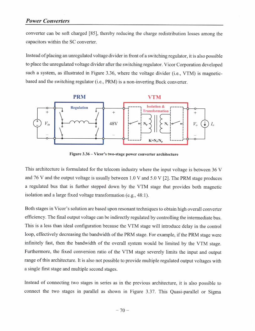
Power Converters
converter can be soft charged [85], thereby reducing the charge redistribution losses among the
capacitors within the SC converter.
Instead of placing an unregulated voltage divider in front of a switching regulator, it is also possible
to place the unregulated voltage divider after the switching regulator. Vicor Corporation developed
such a system, as illustrated in Figure 3.36, where the voltage divider (i.e., VTM) is magnetic-
based and the switching regulator (i.e., PRM) is a non-inverting Buck converter.
PRM VTM
Regulation ........ Isolation & -------
4 +Transformation:
Vin 48V N, VN, V
K=N,/N I --------
Figure 3.36 - Vicor's two-stage power converter architecture
This architecture is formulated for the telecom industry where the input voltage is between 36 V
and 76 V and the output voltage is usually between 1.0 V and 5.0 V [2]. The PRM stage produces
a regulated bus that is further stepped down by the VTM stage that provides both magnetic
isolation and a large fixed voltage transformation (e.g., 48:1).
Both stages in Vicor's solution are based upon resonant techniques to obtain high overall converter
efficiency. The final output voltage can be indirectly regulated by controlling the intermediate bus.
This is a less than ideal configuration because the VTM stage will introduce delay in the control
loop, effectively decreasing the bandwidth of the PRM stage. For example, if the PRM stage were
infinitely fast, then the bandwidth of the overall system would be limited by the VTM stage.
Furthermore, the fixed conversion ratio of the VTM stage severely limits the input and output
range of this architecture. It is also not possible to provide multiple regulated output voltages with
a single first stage and multiple second stages.
Instead of connecting two stages in series as in the previous architecture, it is also possible to
connect the two stages in parallel as shown in Figure 3.37. This Quasi-parallel or Sigma
- 70 -

Power Converters
architecture has some interesting features and was originally developed for the 12 V to 1.0 V
voltage regulator market (VRM) [103]. As before, there is an unregulated transformation stage
(i.e., DCX) and a regulated stage (i.e., BUCK).
However, the parallel arrangement allows for a more efficient delivery of power to the load since
each stage only carries a faction of the total power delivered to the load. The amount of power
each stage processes is set by the input voltage ratio.
h;.1
DCX
Vi" I N 1
"i hn.2 BUCK I0
+-T
Vin2 F I,
Figure 3.37 - Quasi-parallel (sigma) power converter architecture
The full converter efficiency can be calculated by the following equation
V VrIH = il ri 2 1 .2 r2 - (3.72)
V V
Ideally, the vast majority of the power would be processed by the high-efficiency DCX stage and
the remaining power would be processed by the BUCK stage. In this situation, the full converter
efficiency would be solely determined by the efficiency of the DCX stage.
The more efficient delivery of power in this architecture does not come without drawbacks. The
stages in the parallel arrangement need to provide larger conversion ratios than the stages in the
series arrangement. Sharing the first stages to provide multiple output voltages is also not possible.
Finally, at least one of the stages needs to be magnetically isolated for the converter to be functional
-71-

Power Converters
and both stages need to be magnetically isolated for the converter to provide magnetic isolation
from the input to the output.
The various two-stage solutions introduced in this section tackle the problem from different angles,
but the key concept is similar - utilize two distinct power converters to achieve superior
performance. Furthermore, there is a gain in performance when the choice of power converter
topologies is synergistic. As with all designs, the choice of architectures depends upon many
factors including the input voltage range, the output voltage range, desired efficiency, desired
power density, and so on.
- 72 -

Chapter 4 - Passive Components
All power converters require energy storage elements to convert power efficiently. Energy can be
stored in either electric or magnetic fields (or, less commonly, in other forms). Typically,
capacitors and inductors are used to storage energy in power converters.
Over the years, numerous structures and materials have been devised to store energy in electric
and magnetic fields. We set the stage in this chapter by first describing the basics of electric and
magnetic materials. After that, we provide a comparison of two energy storage structures and their
typical use case. Furthermore, Appendix B and C give a detailed discussion on barium titanate and
soft ferrites, both of which are very well suited for the power architecture to be introduced in
Chapter 5.
4.1 Energy Storage
Work must be done by an external stimulus to establish an electric field within a capacitor. The
energy stored in the electric field of the capacitor is the integral of the instantaneous power.
Assuming that the capacitor has zero charge at t = Doo, the energy stored in the capacitor at time t
is given by
tt t 1v-) IC~)
U,(t)= f P(v) dv = fv(r)i(v)dr= fv(r)A dr= Cv(t)2 (4.1)U U dv 2
where
Coce. (4.2)
Therefore, a higher permittivity c allows a greater amount of charge to be stored on the capacitor
at a given voltage.
Similarly, work must be done by an external stimulus to establish a magnetic field within an
inductor. The energy stored in the magnetic field of the inductor is the integral of the instantaneous
power. Assuming that the inductor has zero current flowing through it at t = EL0, the energy stored
in the inductor at time t is given by
- 73 -

Passive Components
U .(t) = [ P(r) dr = v(r)i(r) dv = f L di(r) i(r) dr = 2 Li(t )2
_ 2 (4.3)
where
L oc u. (4.4)
Likewise, a higher permeability p allows a greater amount of flux to be stored in the inductor at a
given current.
Therefore, the energy storage capacity of a capacitor is proportional to its capacitance while the
energy storage capacity of an inductor is proportional to its inductance, both of which can be
increased by using electric or magnetic material.
4.1.1 Electric Material
Electric materials can be used to store energy in electric fields. They are typically electrical
insulators that are easily polarized by an external electric field E. In these materials, an internal
polarization field P is created when the electric dipole moments within the material align with an
applied E. Consequently, the total electric flux density D inside an electric material is given by
D=e 0 EDP, (4.5)
where the permittivity of free space is
co = 8.85418x10⁻¹² (F/m) . (4.6)
The first term on the left represents the contribution of the applied electric field, while the second
term on the right represents the contribution of the induced polarization field within the electric
material. This type of material is often referred to as a dielectric as well.
Alternatively, D can be expressed in terms of relative permeability cr as
D=8r60 E , (4.7)
where
- 74 -
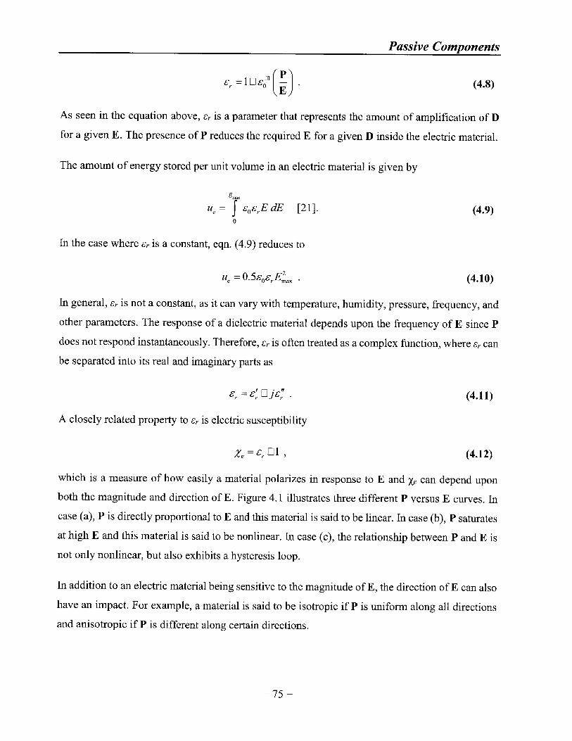
Passive Components
6r lD8jj . (4.8)E
As seen in the equation above, c, is a parameter that represents the amount of amplification of D
for a given E. The presence of P reduces the required E for a given D inside the electric material.
The amount of energy stored per unit volume in an electric material is given by
E.
Ue = f eE dE [21]. (4.9)0
In the case where Cr is a constant, eqn. (4.9) reduces to
ue = 0.5eoeEm . (4.10)
In general, cr is not a constant, as it can vary with temperature, humidity, pressure, frequency, and
other parameters. The response of a dielectric material depends upon the frequency of E since P
does not respond instantaneously. Therefore, Cr is often treated as a complex function, where Cr can
be separated into its real and imaginary parts as
!r r= E j (4.11)
A closely related property to cr is electric susceptibility
Ze = sr 0l , (4.12)
which is a measure of how easily a material polarizes in response to E and Xe can depend upon
both the magnitude and direction of E. Figure 4.1 illustrates three different P versus E curves. In
case (a), P is directly proportional to E and this material is said to be linear. In case (b), P saturates
at high E and this material is said to be nonlinear. In case (c), the relationship between P and E is
not only nonlinear, but also exhibits a hysteresis loop.
In addition to an electric material being sensitive to the magnitude of E, the direction of E can also
have an impact. For example, a material is said to be isotropic if P is uniform along all directions
and anisotropic if P is different along certain directions.
- 75 -

Passive Components
PtE
P
tE
~-+OE /
Pt
-E
I
(b) Nonlinear
Figure 4.1 - Various types of electric polarization
(c) Hysteresis
Electric moments are induced in dielectric material through a few different mechanisms. The threeprimary polarization mechanisms are electronic, ionic, and orientation, all three of which areillustrated in Figure 4.2.
E
Q _
+- P E tP
~0 +
(a) Electronic (b) Ionic
Figure 4.2 - Three polarization mechanisms
(c) Orientation
The first mechanism that we discuss is shown in Figure 4.2a. In electronic polarization, an appliedelectric field displaces the electron cloud's center of charge with respect to the atom's nucleus.This distortion induces a dipole moment within the material. Consequently, this type ofpolarization is also known as atomic polarization. The strength of the polarization depends uponthe asymmetry in the electron orbitals. For example, this effect is extremely weak in the case ofhydrogen (i.e., spherical symmetry), but quite strong in crystalline silicon due to its sp3 hybridorbitals. The dielectric constant of silicon is twelve, which comes exclusively from electronicpolarization. Even so, this type of polarization is typically the weakest of the three polarization
mechanisms.
- 76 -
(a) Linear
..-Oaj

Passive Components
The next major mechanism that we explain is shown in Figure 4.2b. This type of polarization
occurs in ionic crystals. For example, in sodium chloride (NaCl), the net polarization is exactly
zero in absence of an applied electric field. This is because every dipole moment has a neighboring
dipole moment with the same magnitude, but in the opposite direction. However, when an external
electric field is applied, the positive and negative ions are slightly displaced from their rest position
in the crystalline matrix, thereby inducing a net dipole moment. Ionic polarization is the strongest
of the three mechanisms. In Appendix B, we discuss a very important ceramic material, which has
a strong ionic polarization component.
The last polarization mechanism we describe is orientation polarization and is illustrated in Figure
4.2c. This type of polarization results from a permanent dipole that can rotate freely within a
material. In thermal equilibrium, the dipoles are oriented randomly, but when an electric field is
applied, the dipoles align with the field to some extent inducing a polarization field. Orientation
polarization is typically limited to liquids. For example, in liquid water every water molecule is a
dipole moment arising from the 104.450 angle between the oxygen and hydrogen atom. These
dipoles are constantly moving around and rotating because they contain thermal energy. If an
electric field is introduced, the dipoles have a tendency to turn into the field; and the stronger the
electric field, the more they turn into it. Water has a dielectric constant of eighty-one so orientation
polarization can be a relatively strong effect.
It is possible that some or all three polarization mechanisms will act simultaneously in a given
material. Electronic polarization, for example, is always present in any material and, if any of the
other mechanisms exist, their effects are superimposed. Additionally, there are few other
polarization mechanisms, which were not discussed because they are much weaker.
4.1.2 Magnetic Material
There are many similarities between magnetic materials and electric materials, which will be
evident in the following section. Magnetic materials are mediums that can be easily magnetized
and can be used to store energy in magnetic fields. When an external magnetic field H (A/m) is
applied, magnetic dipole moments within a magnetic material align creating an internal
magnetization field M (T). Consequently, the total magnetic flux density B (T) inside a magnetic
medium is given by
- 77 -

Passive Components
B=pOHDM, (4.13)
where the permeability of free space is
po = 47x10 7 (H/m) . (4.14)
It is important to note that the units for M are the same as B. This is not always the case; sometimes
M has units of A/m.
The first term on the left represents the contribution of the applied magnetic field, while the second
term on the right represents the contribution of the induced magnetization field within the magnetic
material. Alternatively, B can be expressed in terms of relative permeability pr as
B= ppuoH ,(4.15)
where
0Mpu, =I 1 . (4.16)
As seen in the equation above, pr is a parameter that represents the amount of amplification of B
for a given H. For example, the presence of M reduces the required H for a given B inside the
magnetic material.
Similar to eqn. (4.9), the amount of energy stored per unit volume in a magnetic material is given
by
H.
Um= popHdH . (4.17)0
In the case were pr is a constant, eqn. (4.17) reduces to
Un = 0.5 pop,.H . (4.18)
In general, pr is not a constant, as it can vary with temperature, humidity, pressure, frequency, and
other parameters. The response of a magnetic material depends upon the frequency of H since M
does not respond instantaneously. Therefore, ur is often treated as a complex function, where pr
can be separated into its real and imaginary parts as
- 78 -

Passive Components
u, = ju ,M" -(4.19)
A closely related property to pr is magnetic susceptibility
Zm = Pr 1 , (4.20)
which is a measure of how easily a material magnetizes in response to H and X," can depend upon
both the magnitude and direction of H. Figure 4.3 illustrates three different M vs. H curves. In
case (a), M is directly proportional to H and this material is said to be linear. Whereas, in case (b),
M saturates at high H and this material is said to be nonlinear. Lastly, in case (c), the relationship
between M and H is not only nonlinear, but also exhibits a hysteresis loop.
M M M
t t t
(a) Linear (b) Nonlinear (d) Hysteresis
Figure 4.3 - Various types of magnetic polarization
In addition to a material being sensitive to the magnitude of H, the direction of H can also have an
impact. For example, a material is said to be isotropic if M is uniform along all directions and
anisotropic if M is different along certain directions.
Magnetization in a material results from atomic loops [107]. Whenever an electron moves, a
magnetic field is produced and if the electron moves in a loop, a magnetic moment is produced.
Let us assume an electron orbits a nucleus in atom as illustrated by Figure 4.4. While the electron
travels about the nucleus, an orbital magnetic moment mo is generated that is normal to the plane
of its orbit. Furthermore, the electron spins about its own axis as it orbits the nucleus, producing a
spin magnetic moment ms that is parallel to the axis of its spin.
- 79 -

Passive Components
le
(a) Orbiting electron (b) Spinning electron
Figure 4.4 - Classical model of a hydrogen atom
It is important to note that this model does not have quantitative significance. However, both
magnetic moments can be calculated using quantum mechanism. As it so happens, ms is exactly
equal to mo in the first Bohr obit, where its magnitude is
jB = 9.27x10⁻²⁴ (A-m2) . (4.21)
This quantity is a natural unit of magnetic moment and is given a special name - the Bohr
magneton.
In reality, an atom contains many electrons each spinning about their own axis and rotating in their
own orbit. The magnetic moment associated with each type of electron motion is a vector quantity.
Therefore, the total magnetic moment of the atom is the vector sum of each electron. If all of the
electrons are oriented such that their moments cancel out, then the material is not magnetic.
However, if there is only partial cancellation and the atom is left with a net magnetic moment, then
the atom is often referred to as a magnetic atom. Materials composed of atoms of this type are
magnetic materials. Furthermore, in solids, the orbital moment is quenched by the strong crystal
field produced by the surrounding atoms or ions in the solid. The strong orbit-lattice coupling often
prevents magnetic moments from turning towards the applied magnetic field, whereas the spin is
weakly coupled to the orbit so it is free to react. Consequently, only the spin contributes to the
magnetization process in a solid [31].
We now discuss the different types of magnetic materials. The first class of materials is called
paramagnetic. They are composed of atoms or ions that have a net magnetic moment due to
- 80 -
___ _ _= - _ - - - - - - - 1-111- 1- 111,111, ---------- - .... ... . .. . . ........ .. - - I ..... . .....

Passive Components
unpaired electrons in partially filled orbitals. The individual magnetic moments within these
materials do not interact magnetically so the net magnetization of the whole material is zero.
However, if a magnetic field is applied there is partial alignment of the atomic magnetic moments
in the direction of the applied magnetic field, resulting in an induced magnetization field.
Typically, when one thinks of magnetic materials, one thinks of iron, nickel, or magnetite. Unlike
paramagnetic materials, the adjacent atomic moments within these materials exhibit very strong
interactions. Powerful "exchange forces" align the atomic moments by altering their spins. This is
effect is very strong: these materials produce magnetization fields that are orders of magnitude
larger than paramagnetic materials under the same applied field. Exchange energy can also
produce either parallel or antiparallel exchange coupling.
(a) Ferromagnetic (b) Antiferromagnetic (c) Ferrimagnetic
Figure 4.5 - Three different magnetic moment alignments
Magnetic materials that exhibit exchange coupling are generally divided into three classes:
ferromagnetic, antiferromagnetic, and ferrimagnetic. The type of coupling depends upon the
composition and crystal structure. Strictly speaking, ferromagnetism refers to materials with
parallel coupling of adjacent atomic magnetic moments as shown in Figure 4.5a. In this class, a
spontaneous magnetization is retained in the absence of an applied magnetic field, giving rise to
permanent magnetic moments. Iron is a common example of this type of material.
Figure 4.5b and Figure 4.5c illustrate situations that involve parallel coupling within layers of
atomic magnetic moments, but antiparallel coupling between layers. If all of the layers in a material
have equal magnetic moments, then the opposing layers cancel out. This type of coupling is
referred to as antiferromagnetic and was first discovered by Louis Neel in 1936 [79]. However, if
-81 -

Passive Components
some of the layers have unequal magnetic moments, then there is a net magnetic moment. Such a
coupling is called ferrimagnetic and was once again discovered by Louis NMel, this time in 1954
[80]. Ferrimagnetism can be thought of as a special case of antiferromagnetism, where the
canceling is incomplete, thus giving rise to spontaneous magnetization. Iron ferrite is an important
example of the class of material, which we discuss in Appendix C.
4.2 Energy Storage Structures
Up until now, we have only discussed the properties of electric and magnetic materials; however,
these materials need to be fashioned into specific structures to store energy. To begin this section,
we calculate the absolute maximum possible energy storage density for both electric and magnetic
materials. This sets an upper bar for which all energy storage structures must be at or below.
For the purpose of this analysis, we are assuming that the maximum electric or magnetic field is
set by the saturation of the material rather than its breakdown field. Therefore, in the case of an
electric material, we have a maximum electric field of
E,,= El sat (4.22)-=P co (6, Ell)
The maximum amount of electric energy storage per volume can be found by substituting eqn.
(4.22) into eqn. (4.9), yielding
p2U ''at r 1 (4.23)
2eo El Ilj
In the case of a magnetic material, we have a maximum magnetic field of
Hst = HMM - M-t (4.24)Pjt(p El)
Similarly, the maximum amount of magnetic energy storage per volume can be found by
substituting eqn. (4.23) into eqn. (4.17), yielding
F2 P, 1Ummti(-2, 0 LL1Lrl (4.25)
- 82 -

Passive Components
We now are going to discuss and contrast two common types of passive components: multi-layer
ceramic capacitors and toroidal inductors.
4.2.1 Multi-Layer Ceramic Capacitors
Multi-layer ceramic capacitors (MLCC) were first developed in the early 1980s and are an
evolution of single-layer ceramic capacitors. They store electric energy in multiple ceramic layers
that typically have a high dielectric constant. Barium titanate (BaTiO3) is often the dielectric of
choice. Because they are surface mount devices (SMD), MLCCs can be placed on printed circuit
boards (PCB) using high-speed auto pick and place machines, resulting in reduced assembly cost
and increased throughput. Prior to their introduction, the principal capacitor types were wet
electrolytic (aluminum and tantalum), solid electrolytic (tantalum), ceramic, film, mica, and paper
capacitors.
The structure of a MLCC is illustrated in Figure 4.6. Within the capacitor, numerous metal
electrodes and ceramic layers are alternately stacked. The internal electrodes are arranged in an
interdigitated pattern with the adjacent electrodes extending to the opposing terminals, while the
non-adjacent electrodes extend to the same terminal. On each terminal, a metalized coating applied
to the exterior faces, called end termination, electrically connects the exposed electrode edges. In
this example, the left side is the positive terminal while the right side is the negative terminal.
Figure 4.6 - Side view of a multi-layer ceramic capacitor
MLCCs have many uses, including filtering, tuning, decoupling, and energy storage. Their use
prevails in the industry because of their high capacitance, small size, low cost, high reliability, and
excellent high-frequency characteristics. There is a concerted effort to increase volumetric
efficiency of MLCCs due to the constant pressure from the electronic industry to add more
functionality in less space.
- 83 -

Passive Components
Various ceramic dielectrics are employed in MLCCs and the Electronic Industries Alliance (EIA)
classifies the capacitor based on the temperature characteristics of the dielectric material. There
are three main dielectric classes - I, II, and III. Class I dielectrics have relatively low dielectric
constants when compared to the other two classes. However, they are linear and very stable across
temperature. Class II and III dielectrics are nonlinear and the first two digits in the EIA code
provide their minimum and maximum operating temperatures. The maximum allowable shift in
capacitance over the allotted temperature range is specified by third digit in the code. A few
common EIA codes are provided in Table 1 for reference [45].
Minimum Operating Maximum Operating Maximum Capacitance ShiftTemperature Temperature
Temp Symbol Temp Symbol Percent Symbol EIA Class
+10 C Z +45 C 2 ±22% S II
-30 C Y +85 C 5 ±15% R II
-55 C X +125 C 7 +22/-56% U III
+200 C 9 +22/-82% V III
Table 4.1 - Common EIA temperature characteristic codes for class II and III dielectrics
Class III dielectrics offer the highest dielectric constants, but their film thickness is limited due to
the severe reduction in their permittivity with grain size. Thus, MLCCs with the highest volumetric
efficiency typically use Class II dielectrics such as X5R [45].
WV
\td
Figure 4.7 - Multi-layer ceramic capacitor structure
/
- 84-

Passive Components
For the purpose of the following analysis, the MLCC structure illustrated in Figure 4.7 is used,
where Wis the width of the electrode, L is the length of the electrode overlap area, NL is the number
of internal electrodes, cr is the relative dielectric constant of the ceramic, and td is the thickness of
the ceramic.
The amount of capacitance in the MLCC structure depicted above is
C = NL (4.26)
where the area of the exposed ceramic is given by
Ad =WxL. (4.27)
The total dielectric stack volume within the MLCC, excluding the thickness of the electrodes, is
given by
volc = tdx Adx NL (4.28)
By plugging eqn. (4.26) into eqn. (4.1), the energy in the capacitor is
=1 co cAd vUC 2 d Lpk (4.29)
The energy stored per volume in the dielectric stack of the MLCC can be found by dividing eqn.
(4.29) by eqn. (4.28), yielding
Ue 1 _S0r 2U - - -t Vpk (4.30)vo4, 2 td
Further, the maximum electric field occurs when
_ V Vpksattd E- I (4.31)
-EO, -o U, 01[E
Therefore, the maximum energy stored per volume in the electric field of the MLCC can be found
by plugging eqn. (4.31) into eqn. (4.30) resulting in
- 85 -

Passive Components
UP2 F_UC,max =v = 2UC L = ] Uex (4.32)
volc 260 _C 31
Thus, a high ucmax can be achieved in a MLCC by utilizing electric material that has both a high
permittivity and a high saturation field. It is important to note that eqn. (4.32) is identical to eqn.
(4.23). Therefore, the MLCC structure can store the maximum amount of energy possible.
However, this is assuming the internal electrodes do not consume space and there is no additional
packaging. Incidentally, when the dielectric layers are very thin, the internal electrodes can take
up the same volume as the dielectric layers.
4.2.2 Toroidal Inductors
As discussed in Section 4.1.2, when current flows through a piece of wire, a magnetic field is
formed. If this wire is looped into a coil, then the magnetic field is concentrated. The simplest type
of coil is a linear coil, also known as a solenoid. However, if the two ends of the solenoid are
looped back on themselves then a toroidal inductor is formed as illustrated in Figure 4.8. The
optimum shape of the toroidal winding is a complex optimization process that depends on the
application [11]. Additionally, the magnetic field can be further enhanced by placing a magnetic
medium, such as a ferrite, in the middle of the coil.
Figure 4.8 - Top view of a toroidal inductor
- 86 -

Passive Components
Besides toroidal cores, there are pot cores, E cores, C cores, and so on. However, due to the
winding construction, toroidal inductors offer one of the smallest solutions by volume and/or
weight. They also produce a relatively small amount of electromagnetic interference (EMI)
because the magnetic flux density B is well contained within the core.
Toroidal cores can be made of many different types of material, of which magnetic materials are
the most common. A majority of magnetic materials fit within one of the following four categories:
ferrites, alloys, powder iron, and amorphous. Table 4.2 illustrates the typical magnetic properties
for each of the four categories.
Properties Ferrites Alloys Powder Iron Amorphous
Initial Permeability 5 - 1.5x10⁴ 5x10 - 3x10⁵ 5-150 3x10³ - 1.5x10⁵
Cure Temperature ('C) 100-500 500 750 210-485
Saturation Flux Density (T) 0.3 - 0.5 0.8 -2.4 1.0 - 1.2 0.55 - 1.0
Coercive Force (Oe) 0.05 0.003 - 3.0 0.003 - 3.0
Loss factor (y/p1 x 10-6)
fs = 1x10 4 Hz 0.5 8 2
fs = I x10 5 Hz 1 80 30
fs = 1x10 6 Hz 25 4000 100
Bulk Resistivity (Q-cm) 10 - 1x100 1 X10-5 IX104 .4x 10-4
Table 4.2 - Properties of various magnetic materials
In general, each type of magnetic material has its own advantages and disadvantages. Take, for
example, magnetic alloys. They have the highest saturation flux density and permeability, which
are good attributes for ac line transformers. However, magnetic alloys are useless at high frequency
because their low bulk resistivity will result in large eddy current losses. Ferrites, on the other
hand, are a great choice for high frequency operation. They are made of a ceramic material, so
their bulk resistivity is high and they also have low core losses at high frequency.
For the purpose of the following analysis, the toroidal inductor structure in Figure 4.9 is used,
where d is the outer diameter of the core, di is the inner diameter of the core, h, is the height of
the core, and Nis the number of turns on the core.
- 87 -

Passive Components
di#I
Ut
I .P
ft ftaM 4 oW e0 - - do
N Turns
h
Figure 4.9 - Toroidal inductor structure
The amount of inductance in the toroidal inductor structure depicted Figure 4.9 is given by
L= p 0 /lr2 k In( 4 .2f di (4.33)
By plugging eqn. (4.33) into eqn. (4.3), the energy in the inductor is
=1I popN 2h c ind) 2UL 2 T iIpk2 2ff d (4.34)
The magnetic saturation flux Bsat of the core at the peak inductor current Ipk sets the number of
turns, which is given by
N = B"d ' .PO Pr Ipk
The total volume of the core can be determined by
voIL ( 4. 3 .1 22
There are three independent parameters, which define volL. Fortunately, there is an optimum shape
for a toroidal core, which has the smallest volume for a given set of electrical specifications. It has
-88-
a a
.
(4.36)

Passive Components
been shown that there are optimum proportions for a toroidal core with a rectangular cross section
and a single-layer winding at high frequency [11]. The optimum height with respect to d, is
k =0.44d, (4.37)
and the optimum inner diameter with respect to do is
di=0.56d . (4.38)
It is important to note that the optimum proportions given above assume a constant volL.
The energy per volume can be found by dividing eqn. (4.34) by eqn. (4.36) and substituting eqns.
(4.37) and (4.38) into the result, yielding
U 2('O.O8559 2UL vL _ 20.08 I,9) . (4.39)LVo1lL \ OY do p
By plugging eqn. (4.35) into eqn. (4.39), the maximum energy per volume stored in the magnetic
field of the toroidal inductor is given by
U 0.53 (BrULma I I,=0 ,, (4.40)
vol. 2po p,
Furthermore, the relation between Msat and Bsat is defined as
Bst = Ma 0 - (4.41)
Therefore, to be consistent with eqn. (4.25), Bsat in eqn. (4.40) is replaced by Msat, resulting in
ULm 0.53st r 0.53xu,,m . (4.42)2 po [ ju, El1(
To achieve a high UL,max in a toroidal inductor, a magnetic material with a low permeability and a
high saturation field is desirable. It is important to note that eqn. (4.42) has a similar form as eqn.
(4.25). Unfortunately, UL,max is 53% smaller than um,max. This is a result of having a non-uniform
magnetic field within the core.
-89-

Passive Components
4.2.3 Component Comparison
We now compare the energy storage density of a MLCC with a BaTiO3 dielectric and a toroidal
inductor with a nickel-zinc (NiZn) ferrite core. We are assuming both materials are operating at a
frequency exceeding 10 MHz and a voltage less than 100 V. To make the comparison, we have
selected reasonable materials parameters for each material as illustrated in Table 4.3.
Structure Material Param 1 Param 2 Energy Density
MLCC Thick Film BaTiO3 er = 3500 Psat = 0.165 C/m 2 439.51 pJ/mm 3
Toroidal N40 (NiZn Ferrite) pr = 15 Msat = 0.270 T 1.1761 pJ/mm3
Table 4.3 - Energy density of magnetic materials vs. electric materials
As discussed in Appendix B, the relative permittivity Cr of a BaTiO3 ceramic will typically be in
the 2000 - 6000 range. The exact value of Fr will depend upon the grain size and processing
conditions, so a value of 3500 is reasonable. On the other hand, the polarization saturation field
was calculated using
0.9Ps= 0, (4.43)
where Po is spontaneous polarization magnitude. In the case of BaTiO3, Po is 0.26 C/m 2 . We are
also assuming that the electric domains are in a lamellar twinning pattern and that the resultant
polarization is approximately 90% of the grain's polarization.
The magnetic parameters were chosen to be representative of a high frequency NiZn ferrite. As
discussed in Appendix C, the relative permeability pr of a ferrite is linked to its operating frequency
through Snoek's law. Therefore, an , of 15 is a reasonable value for a core material with a
resonance frequency of larger than 10 MHz. Furthermore, depending upon the compositions of the
NiZn ferrite, its net magnetic moment per molecule ptH is between 2pB and 5pB. Based upon eqn.
(C.2), this results in a magnetic saturation field Msat in the 255 - 640 mT range.
The energy density value for the MLCC was calculated by substituting 6r and Psat into eqn. (4.32),
whereas, the energy density value for the toroidal inductor was calculated by substituting p, and
- 90 -

Passive Components
Msat into eqn. (4.42). Based upon Table 4.3, there is approximately three orders of magnitude
difference between the energy storage density of these two structures.
To verify these results, key performance parameters from a commercial MLCC from Samsung and
a commercial chip inductor from Taiyo Yuden are shown in Table 4.4. These components were
chosen because they have a similar case size and are best in class.
Part Vendor Value Rating Resistance L x W x H Energy
CL21A476MQCLRNC Samsung 47.0 pF 6.3 V 2 mD 2 x 1.25 x 1.00 mm 375.8 pJ
NM2012NR82M-T Taiyo Yuden 0.82 p1H 1.2 A 85 mQ 2 x 1.25 x 0.85 mm 0.364 pi
Table 4.4 - Key parameters from a commercial MLCC and a commercial chip inductor
As the dc electric field within a ferroelectric capacitor approaches the saturation value of the
material, the permittivity reduces, thereby reducing the effective capacitance of the MLCC. This
effect is more pronounced when the energy density of the capacitor is very high. The energy of the
commercial capacitor was calculated from the capacitance versus dc bias voltage curve in the
datasheet using
V. V.
U, = vi dr= Cv dv= rm x Civ . (4.44)0 0 jen
The ferrimagnetic material within the commercial chip inductor has similar behavior to the
ferroelectric material. As the dc magnetic field approaches the saturation value, the permeability
reduces, thereby reducing the effective inductance. The energy of the commercial inductor was
calculated from the inductance versus de bias current in the datasheet using
Im I.
U, = f vi di-= f Li di= mx L, (4.45)0 0 n ien
Based upon the data in Table 4.4, the energy density of the MLCC is 150.31 pJ/mm 3, in contrast
to 0.171 ptJ/mm 3 for the chip inductor. Moreover, the series resistance of the chip inductor is 42.5
times larger than the MLCC.
-91-

Passive Components
Compared to the data from Table 4.3, the energy density of the commercial MLCC is
approximately three times lower than the ideal MLCC calculation, whereas the energy density of
the commercial chip inductor is approximately seven times lower than the ideal toroidal inductor
calculation. There are two major reasons for these discrepancies. First, the ideal calculations do
not account for the space taken up by either the metal electrodes in the MLCC or the metal winding
in the toroidal inductor. Second, the ideal calculations assume both the permittivity and
permeability of the materials are independent of the dc bias. Additionally, it is unclear if the chip
inductor is a toroid; it is mostly likely a solenoid.
Furthermore, there is decent agreement on the ratio of energy density between the MLCC and
toroidal inductor. The values in Table 4.3 result in a 374-fold difference in energy density, while
the values in Table 4.4 result in an 878-fold difference in energy density.
The large difference in energy density is a direct consequence of barium titanate having a much
larger saturation field than soft ferrites. Lowering the permittivity or permeability of either material
can boost the energy density, but this affects the impedance and/or dc resistance of the passive
component so it is not an acceptable solution. Given the aforementioned constraints, the energy
density of electric material will remain two to three orders of magnitude larger magnetic material,
unless a new high frequency magnetic material with a large saturation field is discovered.
- 92 -

Chapter 5 - Split-Power Architecture
The main function of a dc-dc power converter is to convert one dc voltage to another dc voltage.
Any type of dc-dc converter can be modeled as an ideal transformer with a conversion ratio of
N2/Ni followed by an output resistance R,, as illustrated in Figure 5.1.
'in N 1 : N 2 Ro Io
+
Vin Vo R
DC-DC Converter
Figure 5.1 - DC model of a dc-dR converter
In this model, all of the losses associated with current passing through resistive elements in the
power converter are lumped together in Ro. This does not include losses that are not a function of
the output current Io, such as capacitive switching losses. Given this simple model, the output
voltage Vo of the de-dc converter can be calculated using
V = 2 X Vin El10RO- (5.1)N,
In the equation above, Vo varies with changes in Io, an effect sometimes referred to as "load
regulation". Furthermore, we can split N2/N1 into two components as
N2 / N = Nt,,an E N,,g -(5.2)
After plugging (5.2) into eqn. (5. 1), we obtain
VK = D\eran x nf2 [I Erej E 1Ao~ E. (5.3)
- 93 -

Split-Power Architecture
Based upon eqn. (5.3), a dc-dc converter can be thought of serving two functions. First, it provides
voltage transformation of the input voltage Vi,, to another dc voltage level at a conversion ratio
Ntran. Second, it provides a mechanism to compensate for deviations in V by varying a regulation
ratio Nreg. In eqn. (5.3), the term on the left represents the voltage transformation component while
the term on the right represents the voltage regulation component.
For reference, a Buck converter provides both of these functions at the same time with the use of
only two switches. In this chapter, we introduce a power conversion architecture where we split
these two functions. We explore the rationale for doing so and then compare this architecture with
traditional power converter topologies.
5.1 Converter Architecture
Figure 5.2 illustrates a two-stage power conversion architecture where the transformation and
regulation functions of a power converter are split, in contrast to being accomplished together in a
single-stage power converter design. In this architecture, the transformation stage and the
regulation stage are highly optimized for their specific functions. From now on, we will refer to
this architecture as the split-power architecture.
Transformation Stage Regulation Stage(Variable & Non-Isolated) (Non-Isolated or Isolated)
+ +m-> ++Vn x -O
Figure 5.2 - Block diagram of the split-power architecture
It is well known that all switching power converters require intermediate energy storage to operate.
A lower bound on the amount of energy is given by eqn. (1.7) in Chapter 1. Assuming the size of
a power converter is dictated by its energy storage elements, there are then two approaches to
reducing the size of the power converter without decreasing its efficiency. Either the amount of
energy required to be stored is decreased or the energy density of the storage elements is increased.
- 94 -

Split-Power Architecture
Traditional switch-mode converters consist of a combination of magnetic and electric storage
elements. The amount of energy storage required in this type of power converter is a function of
the switching frequency. The higher the switching frequency, the lower the energy storage
requirement; the lower the switching frequency, the higher the energy storage requirement.
Increasing the energy density of passive components can take lot of time and money. However,
with the continued pressure of miniaturization in the portable electronic space, there has been some
increase in the performance of inductors and capacitors.
Instead of trying to increase the energy density of inductors, which are the real bottleneck, the
energy density of the overall system can be increased by storing the energy in electric fields rather
than in magnetic fields. It was shown in Chapter 4 that - at least in systems at typical power supply
voltages and currents - capacitors provide energy storage densities at least two orders of magnitude
higher than inductors at given present technological constraints. This approach tackles the energy
density requirement from a different angle.
The split-power architecture utilizes the two previously mentioned size reduction approaches to
increase power density without sacrificing efficiency. The transformation stage provides the
voltage transformation function, so it requires the bulk of the energy storage. Consequently, this
stage benefits greatly by using switched capacitor networks. The regulation stage, on the other
hand, provides the voltage regulation function. To do this efficiently, this stage requires a
combination of magnetic and electric storage elements. Due to the low energy density of magnetic
components in general, the regulation stage runs at a high frequency to reduce the energy storage
requirements.
Unlike previous two-stage architectures, such as those discussed in Section 3.3, the split-power
architecture is based upon the key idea that a slow capacitive-based transformation stage does the
"heavy lifting" in voltage conversion, while a fast LC-based regulation stage removes the slack in
the output. As the age-old saying goes, the whole is greater than the sum of the parts.
Furthermore, this power conversion architecture is extremely flexible and allows for designs with
different requirements. For example, designs that require magnetic isolation could be achieved by
using a magnetic isolated fly-back converter, while designs that require multiple regulated output
- 95 -
Split-Power Architecture
voltages could be accomplished by using multiple separate regulation stages and a single
transformation stage.
5.2 Transformation Stage
The sole purpose of the transformation stage is to provide an efficient intermediate voltage Vx that
is smaller than the input voltage VGn and varies less (in the ratio of minimum to maximum) than
Vi,,. The transformation stage, however, does not need to regulate V, tightly; it simply needs to fall
within a desired voltage window. If V is too high, then the switches in the regulation stage might
be overstressed. Conversely, if V, is too low, then there might not be enough headroom for the
regulation stage to provide a regulated output voltage Vo. To reduce the burden upon the regulation
stage, it is desirable for the transformation stage to convert Vi, to Vo as close as possible while
leaving enough headroom for the regulation stage. Unfortunately, this increases the burden upon
the transformation stage. Therefore, an optimum transformation stage design would balance the
burden upon each stage.
As previously mentioned, an SC power converter is an ideal choice for the transformation stage.
Through the exclusive use of capacitors, this type of power converter provides very efficient power
conversions at distinct conversion ratios. SC converters consist of a network of switches and
capacitors. Energy is transferred from the input to the output by cycling the SC network through
different topological states. A detailed analysis of their operation is given in Section 3.2.
A SC converter can be modeled as an ideal transformer with a finite output resistance Ro and a
common ground as shown in Figure 3.22 [10]. Due to the lack of a magnetic element, there is no
efficient means to continuously vary the conversion ratio Ni:N2 in an SC converter. For this reason,
SC converters provide a relatively poor output voltage regulation in the presence of a varying input
voltage or output voltage target. However, if the SC network is dynamically reconfigured to
different conversion ratios, then it is possible to maintain V, within a specified window as Vi, varies
across a wide range.
Figure 5.3 illustrates a sample V, window that has a maximum value of 2.0 V and minimum value
of 1.0 V. Given a Vi, range of 1.0 V to 6.0 V, a total of four distinct conversion ratios (1:1, 1.5:1,
2:1, and 3:1) are required. In general, the maximum voltage and minimum voltage of V, window
- 96 -

Split-Power Architecture
of the transformation
accomplish this task.
stage can be tailored to fit the regulation stage. Various control schemes can
2.5
a0
a
2
2.0 -_ _ _ _ _
1.51
-1.0 :1.0
- 1.5 :1.0-2.0 :1.0
-3.0 :1.0
0.5
0.01.0 2.0 3.0 4.0
Input Voltage (V)5.0 6.0
Figure 5.3 - Intermediate voltage Vx window (reconfigurable SC converter required)
The selection of the SC topology depends upon the requirements of the transformation stage and
the available passive components. For example, the number of capacitors in an SC converter
determines both the maximum conversion ratio and the total possible number of distinct
conversion ratios [68]. In the end, the design of the transformation stage is influenced by many
factors, including the Vi range, the V range, desired efficiency, desired power density, and so on.
5.3 Regulation Stage
The role of the regulation stage is to convert the intermediate voltage Vx to a regulated output
voltage V. It is desirable to provide a high-bandwidth regulation of V. To optimize the design of
the regulation stage, the conversion ratio should typically be small, usually less than 2:1. Eqn. (3.7)
illustrates that as the conversion ratio in a Buck converter decreases, the amount of power needed
to be inverted also decreases. Normally, in a well-formed design, the size of the regulation stage
should be approximately equal to the size of the transformation stage. Therefore, to make up for
the lower energy density of magnetic material, the switching frequency of the regulation stage
should be higher than the transformation stage.
- 97 -

Split-Power Architecture
A switch-mode power converter is an ideal choice for the regulation stage. This type of power
converter can precisely regulate Vo by varying the duty cycle D. Unfortunately, switch-mode
converters require at least one inductor and one capacitor. One common approach to reducing the
energy storage requirement is to increase the switching frequency. In general, the switching
frequency in a switch-mode power converter sets the required inductance and capacitance. If the
switching frequency is high, the filter inductor and capacitor are small in value and therefore small
in size.
For example, if a two-level synchronous Buck converter is chosen, it can be designed to operate
efficiently at a relatively high frequency enabling small passive component selection and high-
bandwidth control. This is a result of CMOS scaling and low-voltage device stresses. It was shown
in Section 3.1.1 that the optimal switching frequency fop, of a synchronous Buck converter with
CMOS devices follows the characteristic
fop = in avi (5.4)
with / ranging from -3.0 to - 2.5 [84]. Thus, high frequency operation is possible because the
supply to the regulation stage is a low voltage with a narrow range.
We now explore how the size of a toroidal filter inductor scales with the switching frequencyfs.
In a two-level synchronous Buck converter, the required inductance can be found by rewriting eqn.
(3.5) as
L = .i(5.5)
fS AiL2
For this analysis, we are assuming a fixed inductor geometry such that the winding resistance and
the inductor volume are held constant. Given this constraint, the inductor core requires a certain
relative permeability Ur to meet the specification set by eqn. (5.5). This value can be found by
equating eqn. (5.5) with eqn. (4.33) and solving for pr, yielding
1 Jjw E ; V 2 / __ 2(.Pr =_I T l 7 (5.6)
' v A L,2 p oN k In( Ei Id,
- 98 -

Split-Power Architecture
As can be seen, ur is inversely proportional to fsw for a given inductor geometry. One method of
tailoring the permeability of a core is by gapping a high permeability core.
Within a toroidal inductor core, the magnetic field B is a function of the radius r as shown by
B(r) - /rONIL (5.7)2rr
Thus, the maximum magnetic field Bmax occurs along the inner radius (0.5di) and when the
inductor current IL is at its peak current Ipk, resulting in
B = B(0.5d) L =pk - .rONk (5.8)
By substituting Ur from eqn. (5.6) into eqn. (5.8), Bmax is
I1 2 [Y, 0 V / V,G JrB m r (5.9)
"a Nh In [d,/d, ) AIL
As expected, eqn. (5.9) shows that Bmax in a two-level Buck converter with a toroidal inductor is
inversely proportional tofs. What is interesting, however, is that when we plot eqn. (5.9) in Figure
5.4 for various size inductors where di is equal to one-half of d, the small inductors start to saturate
unlessfi, is high enough.
-do=0.5mm-do=1.0mm-do=1.5mmn
1000.0 -do=2.0mParam Value
Vin 2.0 VV0 1.0 V
B pk 2.5 A
AIL,2 1.0 AN 6.0
- - 0.5B . -SB- - - - -
hc 0.4 mm100.03.0 6.0 9.0 12.0 15.0 18.0 21.0 24.0 27.0 30.0
Switching Frequency (MHz)
Figure 5.4 - Maximum flux vs. switching frequency for various Table 5.1 - Parameters fortoroidal inductors Figure 5.4
- 99 -

Split-Power Architecture
Therefore, one fundamental reason that fs, must be increased as the size of the inductor is
decreased, is to prevent the core from saturating. Other considerations in sizing toroidal inductors
for very high-frequency operation include core loss limitations on efficiency; Han and Perreault
[47] consider core loss effects on sizing explicitly, for example.
Furthermore, there are numerous other switch-mode topologies suitable for the regulation stage.
Some additional options include a fly-back converter, a three-level Buck converter [119], a multi-
phase Buck converter, and so on. Ultimately, the design of the regulation stage depends upon many
factors, including the V range, the V, range, desired efficiency, desired power density, and so on.
5.4 Silicon Utilization
There are many facets to a power converter: it should be small, efficient, and fast. Cost is also
important and is typically dependent upon the semiconductor area required. In this section, we
explore the how the power switch area required correlates to the power loss in the split-power
architecture.
The area of a MOSFET in a given CMOS process, based up eqn. (2.15), is given by
AFET c GV 2 , (5.10)
where G is conductance of the MOSFET and V is the breakdown voltage of the MOSFET. The
total power switch area required is the summation of all of the MOSFET as shown by
A, = k IG, ., (5.11)
where k is a fabrication constant related to the minimum feature size of the process.
It has been illustrated by Seeman that a useful metric to compare the silicon utilization of different
power converters topologies [95, 96] is defined as
FSL ~ , G2 ' (5.12)
where the conductive power loss in the switch is represented as
-100-

Split-Power Architecture
P = _IR 0 . (5.13)
In its current form, it is hard to tell that the MFSL metric represents how effective silicon is utilized
(with a larger number representing better utilization). However, by inserting eqns. (5.11) and
(5.13) into eqn. (5.12), MFSL can be can be written as
=P _2 )(k IMFSL ) ) (5.14)
Thus, MFSL is inversely proportional to its conductive power loss Pres and its silicon area Asi. Stated
another way, given a fixed Asi, a topology with a higher MFSL will have lower conduction losses.
Initially, the MFSL metric was developed to compare various SC topologies operating in FSL, hence
the name. However, any type of dc-dc converter topology has a MFSL that represents - in some
manner - conduction loss effects. For example, a Buck converter's MFL is given by
MFSL,BI DVLH (5.15)NNN~D11
The conversion ratio N is defined as the voltage gain when it is a step-up converter and current
gain when it is a step-down converter. For example, in the case of a Buck converter, the conversion
ratio is the inverse of the duty cycle D as represented by
1N = .(5.16)
D
For reference as shown in Seeman and Sanders [96], the cascade multiplier's MFSL is given by
MFSL,CM N 2 N (5.17)32DVND1L
Based upon eqn. (5.15) and eqn. (5.17), it can be seen that MFSL,B1 is equal to MFSL,CM when N is
equal to two. Therefore, the cascade multiplier has a superior MFSL when N is greater than two.
Also, as N approaches infinity, MFSL,B1 approaches zero, whereas, MFSL,CM approaches 1/32.
As N gets large, the performance of a Boost or Buck converter suffers. This is captured in the fact
that MFSL decreases with N in eqn. (5.15), and is also reflected in other analyses of switch-mode
- 101 -

Split-Power Architecture
converters [56]. In principle, this limitation can be partially alleviated by connecting numerous
low-gain stages in series as illustrated in Figure 5.5.
1: N
----------------- -----------------------------------I11: N, ROJ 1 : N2 Ro.2 I : N, Ron I2
V1 V2 R
Stage 1 Stage 2 Stage n
Figure 5.5 - Diagram of a multi-stage power conversion architecture
In the multi-stage architecture shown above, N is the product of N of each stage as given by
n
N=flN. (5.18)j=l
An output resistance RFSL,+ of the multi-stage architecture can then be calculated based upon the
MFSL,j metric of each stage resulting in
RFSL,= El ,(5.19)Xj, j=1 MFSL,j (N1 )f,8
where
X,,, = iGV 2 (5.20)IESW
and 8j is the fraction of Xt used in the jth stage. Therefore, the MFSL metric for the multi-stage
architecture can then be calculated using
MFSLU X V N= = M N. (5.21)'fnXetialseFSL _hj=g MFSL,j n
If n identical stages with a gain of N01n are connected in series then
- 102 -

Split-Power Architecture
MFSLnG MFSL DN ' (5.22)n
Thus, the MFSL metric for two series connected Buck converters is
MFSLBIRD1MFSL,B2 DVilH 4N1/2 I ' (5.23)
4 4N1/2 [F 7 I 2
while the MFSL metric for three series connected Buck converters is
MFSL,BI [1FN PMFSL,B3 -Y]- 9N13Ki1 r (5.24)
Instead of connecting identical stages, it is actually far more advantageous to connect a cascade
multiplier followed by a Buck converter. In the split-power architecture, its R, is given by
N2 N2RFSLSP = N 1 M (5.25)
FP M FSL,CM Vtran [ toty FSL,B reg tot 7try j
and its MFSL is given by
1- 1MFsLsp (N) = (5.26)
FSPMFSL,CM tranE MFSL,BI ' reg
where the weighing parameter y is a number between zero and one. By substituting eqns. (5.15)
and (5.17) into eqn. (5.26), where Ntran=[N/21 and Nreg=N/[N/2], eqn. (5.26) can be rewritten as
32[[N/2] LAO N N FN/2 lI1 (.M ssBDV !;/] -FN2]rD . (5.27)MFSL, SP | N/2 |2 y |[N/2] [I Oy7
Please note, the ceiling function [x] returns the smallest integer that is greater than or equal to x.
Figure 5.6 plots five different MFSL metrics on a log-log scale. The Dickson charge pump is a
specific implementation of a cascade multiplier as discussed in Section 3.2.2. Like all SC
- 103 -

Split-Power Architecture
converters, the Dickson charge pump only converts power efficiently at integer ratios so there are
dots on the graph for this converter instead of a continuous line.
0.100
-SP ARCH
-BUCK-IX
-BUCK-2X
-BUCK-3X
x DICKSON
2 4 6 8 10 12 14
Transformation Ratio (N)
16 18 20
Figure 5.6 - Silicon utilization metric (MFSL) vs. transformation ratio (N) - larger is better
As can be seen, cascade multipliers have the highest MFSL metrics and thus utilized silicon the best.
Unfortunately, the lack of arbitrary conversion ratios limits the usefulness of the Dickson charge
pump. However, the Buck converter performs quite well at low conversion ratios and its reach can
be expanded by cascading multiple stages (e.g., two times and three times).
The split-power architecture with a y of one-half performs admirably across N because it is a
combination of a low-gain Buck converter and a cascade multiplier. It also does not have the
integer limitation of a cascade multiplier and is thus an excellent general-purpose solution when
the conversion ratio N is above four.
5.5 Summary
In this chapter, we introduced a new architecture where the transformation and regulation functions
of a power converter are split. The transformation stage provides the dominant portion of the
voltage conversion while a fast LC-based regulation stage enables efficient regulation of the output
with a variable conversion ratio. The transformation stage can be implemented with high-voltage
devices and operated at a relatively low frequency (e.g., 1.0 MHz) commensurate with the
-104-
cn
0.010
0.001
X

Split-Power Architecture
capabilities of high-voltage devices. In comparison, the regulation stage can be implemented with
low-voltage devices and operated at considerably higher frequencies (e.g., 100 MHz).
In doing so, this power conversion architecture can take advantage of modern commercial CMOS
processes and the surrounding infrastructure. One option to achieve a very high degree of
integration is to realize the converter in a monolithic process with multiple voltage options (e.g., a
process providing for thick oxide and/or extended drain transistors in addition to low-voltage core
devices). Alternatively, a multi-chip approach can be used in which the two stages are implemented
in different processes, each optimized for their respective functions.
The split-power architecture enables power converters to achieve both a very small size and high
efficiency along with high control bandwidth. It accomplishes this by combining the strengths of
switched capacitor techniques (small size, light-load performance) with the high efficiency and
good regulation of conventional switch-mode power converters.
- 105 -

Chapter 6 - Prototype Circuit Design
A prototype dc-dc power converter IC has been created to demonstrate the excellent performance
and superior power density of the proposed converter architecture. The IC was fabricated in a
commercial 180 nm CMOS process, which includes both low-voltage (2.0 V) and high-voltage
(6.0 V) devices. All of the power devices and control circuits are monolithically integrated onto a
single IC to minimize the size of the silicon real estate while also maximizing the electrical
performance of the prototype power converter. Figure 6.1 illustrates a block diagram of the power
converter.
C, C2 CC
VENBK
VEV,,
VEELV VE ICVEE
M, M3 M,
Fiur 6.1.... 1 Blc diga.ftepooyeI
_r _ '7MH G1l91 93 406 DRIVER
C;1 Ci, MM C L K s
-4 -7 GE .
S9 M2 95 M 5 CRVE
ISe O -CR 9 HGH- SCC OC FREQ OSC UC
GEN _92
VJD 9 VREF
VBG VER"""S Silicon IC
VsE VEsc VESEL
Figure 6.1 - Block diagram of the prototype IC
The prototype power converter was designed to operate over the ranges given in Table 6.1. The
voltage and power levels were chosen so the converter could be used in a wide variety of
applications. For example, the input voltage Vin range of 2.7 V - 5.5 V allows the power converter
to work with most lithium-ion battery chemistries. Likewise, the output voltage V range and
power level are suitable for the vast majority of digital electronics, such as mobile application
processes or digital signal processors (DSP).
-106-

Prototype Circuit Design
Parameter Operating Range
Vin 2.7 V - 5.5 V
VO < 1.2 V
PO 2.4 W
Table 6.1 - Prototype power converter operating range
In this chapter, we discuss the design process of both the transformation and regulation stages. We
then explain the design methodology for the gate drivers since they are used in both power stages.
Next, we cover the control design; and, in the last section, we bring everything together with full
chip simulations.
6.1 Transformation Stage Design
The purpose of the transformation stage in the prototype converter is to efficiently provide an
intermediate voltage V rail that varies over a narrow range of low voltages as the input voltage
varies over a wider range of higher voltages. To achieve this behavior, a reconfigurable series-
parallel SC converter was selected. As illustrated in Figure 6.1, the SC converter is composed of
power MOSFETs Mi - M and energy storage capacitors Ci - C3. It can be reconfigured into two
distinct step-down ratios (1/3 and 1/2).
C1 C2
SC T ~ R
(a) V2/V1=1/3
C,
V1 +
+
V2 V1
V1C2+ C3 R V2
CT C2 C 3 R V2
(b) V2/V=1/3
C1 ~C2 ~r&C3 R V2
(c) V2/V1=1/2 (d) V2/V1=1/2
Figure 6.2 - Charge and discharge configuration for two step-down ratios
-107-

Prototype Circuit Design
Figure 6.2 shows the two different SC network configurations for each voltage conversion ratio.
In case (a) and case (c), the capacitors are charged, while in case (b) and case (d), the capacitors
are discharged.
The transformation stage is designed for an input voltage Vin range of 2.7 V - 5.5 V. During steady-
state operation, the maximum voltage Vmax any of the devices in this stage are exposed to is 2/3 Vin
and certain devices are exposed to less voltage as shown in Table 6.2. To ensure reliability, Mi -
M7 must be able to block the required voltage for both configurations. For example, Mi must be
rated for 2/3 Vin, even though it is only exposed to 1/2 Vi when the SC converter is in the 1/2 step-
down configuration.
Vin/Vx M1 M2 M3 M4 Ms M6 M7
1/3 99 99 6P (9 ( 99 9
1/2 99 (P (0 9 ON ON OFF
2 2 1 1 2 1 1
3 3 2 2 3 3 2
Table 6.2 - Voltage stresses of the reconfigurable SC converter for two step-down ratios
The maximum desired Vin of the prototype power converter is 5.5 V, so the IC process must have
devices with a voltage rating of at least 3.66 V. Therefore, a process with two different device
flavors was selected. It has low-voltage core devices with a maximum rated voltage of 2.0 V and
high-voltage 10 devices with a maximum rated voltage of 6.0 V. The process is in a captive 180
nm CMOS foundry from National Semiconductor (now part of Texas Instruments). The low-
voltage devices are ideally suited for the regulation stage, while the high-voltage devices are
suitable for use in the transformation stage. For simplicity, all of the power devices within the
transformation stage utilize the high-voltage device flavor, even though M3, M 4, M6 , and M7 could
have been implemented using lower voltage devices.
The transformation stage is controlled such that V never exceeds 2.0 V and is never below 1.5 V.
This is important because the regulation stage, which follows the transformation stage, is built
using the low-voltage core devices with a maximum rating of 2.0 V. Also, the lower 1.5 V
specification ensures that the regulation stage will have enough headroom to regulate an output
- 108 -

Prototype Circuit Design
voltage V, of at least 1.2 V. With appropriate control, the regulation stage will be able to operate
effectively up to at least a 90% percent duty cycle, yielding a maximum output voltage of 1.35 V.
To design a well-balanced transformation stage, we now identify the major power loss
mechanisms. The main sources of power loss in the SC converter stage are in Mi - M7 and their
gate drivers. The losses associated with C1 - C3 are small compared to the other losses since
MLCCs have very low equivalent series resistance (ESR).
In general, the loss in a MOSFET can be divided up into static losses and dynamic losses. The
static losses occur when the MOSFET is conducting, whereas the dynamic losses occur when the
MOSFET is switching (including overlap loss, device capacitor discharge loss, and gating loss).
As the names would suggest, the static losses are independent of the switching frequency and
dynamic losses are proportional to the switching frequency.
The conduction losses in a SC converter can be calculated using
_cond,sc = IxRo , (6.1)
where the output resistance R, accounts for all the power loss in the charging/discharging of the
energy transfer capacitors and IA is the root-mean-square (RMS) current at the output of the stage.
Typically, this loss will be dissipated in the on-resistance of the power MOSFETs and the ESR of
the capacitors. A detailed description of the equations required for calculating R, is given in
Section 3.2.1. It is important to note that Ro is only a function of parasitic device resistances when
the switching frequencyfsc of the SC converter is high enough such that it is operating in the fast-
switching limit, or FSL.
Within the transformation stage, the dynamic losses in Mi - M7 are given by eqns. (6.2) through
(6.5). Each device has a specific gate charge denoted by Qgo,i and specific on-resistance denoted
by Ron0o,. Both of these are parameters determined by the IC process. Furthermore, in CMOS
technology, the gate charge Qgi and its corresponding on-resistance Ron,i form a constant that is
proportional to the square of their blocking voltage as shown in eqn. (2.10). The desired ratio of
Ron,i to Qgi for device M is set by the device width W selection.
-109-

Prototype Circuit Design
In the SC converter, M - M are driven by a gate driver with its supply voltage Vr,,i provided by
Vi,. Since a gate driver can be thought of as a voltage source charging a MOSFET's gate capacitor,
more energy is required to charge the gate than is actually stored. A detailed explanation is given
in Section 3.2.1. Consequently, the energy loss charging the gate capacitance of M - M 7 is
7 ly7'[
Ugte = EFdrv,iQg,i L Vn QgOiW . (6.2)
The source and drain regions in a MOSFET each consist of a p-n junction. The amount of charge
consumed by the junction of M is a function of the specific junction charge denoted by Qjo,i and
the width W of the device. Thus, the energy loss charging the junction capacitance of M1 - M7 is
given by
7 7
'= [Y ,Q [} Z fQIE,W , (6.3)
where Voffi is the voltage that M blocks when turned off. Similar to what happens when charging
the gates, more energy is required to charge the junction charge Q;,i than is actually stored.
The individual driver loss Pdri for M is given by eqn. (6.36) and the total driver power loss in the
transformation stage is
7
dv,sc = dri (6.4)i=1
The total dynamic loss in the transformation stage is the summation of all of the power loss
components, which are proportional tofsc as given by
dn,sc = Wgate j uncI ] P drv,sc (6.5)
The total power loss in the switched capacitor stage is
loess,sc = cond,sc dyn,sc (6.6)
Once Pos, is known, the efficiency of the transformation stage can be calculated using
-110-

Prototype Circuit Design
Pqse = , (6.7)
P, E Fj,
where Px is the output power of the SC converter.
To optimize qs while also providing a high power density, proper W,fsc, and C1- C3 values must
be chosen. IffSC is too low, then Pcond,sc dominates; and iffsc is too high, then Pdy,sc dominates. In
addition, the value of C1 - C3 affects Ro of the SC converter when operating in SSL and the location
of the transition point between SSL and FSL.
Selecting the capacitance of Ci - C3 is a good place to start the optimization process. To maximize
efficiency, MLCCs with the largest capacitance in a 0402 case size were chosen. High-density
4.7 gF MLCC from Taiyo Yuden (AMKl05ABJ475MV-F) happened to be the highest. They also
had a relatively low ESR of 2.41 mK2. The maximum dc voltage on the capacitors during normal
operation is 2.0 V. This corresponds to a capacitance de-rating factor of 45% from the
manufacturer's datasheet, yielding an effective capacitance of 2.1 pF. The high degradation in
capacitance at such a low dc voltage is a result of the high electric fields within the capacitor. This
is a direct consequence of having a large capacitance in a small case.
10.00-Wn=80 mm
-- Wn=120 mm
-Wn=160 mm1.00 -Wn=200 mm
-Wn=-240 mm
Rout Loss
0.01
Dynamic Loss
0.00-
Frequency (Hz)
Figure 6.3 - Power loss of transformation stage when Vi= 5.4 V and P = 2.4 W
- 111 -

Prototype Circuit Design
To aid in selecting the proper Wi andfs0 , Figure 6.3 illustrates Pcondsc and Pdyn,sc across fc, where
the width of M2 - M7 is denoted by Wn. The SC converter is utilizing the previous 4.7 pF capacitor
selection. Furthermore, the operating conditions for this frequency sweep were chosen to be the
most demanding. This corresponds to a 3:1 step-down ratio, an input voltage of 5.4 V, and an
output power of 2.4 W.
As can been seen from the Figure 6.4, Pdynsc increases withfsc while Pcondse decreases withfsc. This
occurs until FSL is reached, at which point the power loss levels off. In FSL, Pondsc is inversely
proportional to width of the devices, in contrast to being independent of device width in SSL.
Usually, the optimalfsc is in the transitional period between SSL and FSL as shown in Figure 6.4.
This makes the design process challenging because there are no accurate closed-form solutions for
R, in this region. To complicate the process further, the optimalfsc should follow in step with Io.
1.0
0.9
0.8
0.7
0.6
0.5_____ ___ -Wn=80 mm ____
E 0.4 -wn10
0.3 -Wn=160 mm-Wn=200 mm
0.2 -Wn=240 mm
0.1
0.0
Frequency (Hz)
Figure 6.4 - Efficiency of transformation stage when Vim= 5.4 V and Px 2.4 W
Based upon Figure 6.4, the optimal fs of the regulation stage at heavy load is approximately
2.0 MHz with a NMOS device width of 80 mm. However, the regulation stage must be efficient
over the full Vin range (2.7 V - 5.5 V). At the lower Vin range, the 80 mm device width selection
results in a high on-resistance for M4. Therefore, we selected a device width of 160 mm for M2 - M7
and a device width of 288 mm for Mi. At a given width, the PMOS devices have a larger on-
resistance than the NMOS devices so Mi had to be wider than M 2 - M7. Consequently, at a supply
-112-

Prototype Circuit Design
voltage of 5.0 V, the corresponding on-resistance of M2 - M7 is 11.9 mQ and the on-resistance of
Mi is 21.4 mQ. Additionally, at the same operating point, M2 - M has a gate capacitance of 291 pF
and a junction capacitance of 29.6 pF while M has a gate capacitance of 517 pF and a junction
capacitance of 53.2 nF.
Table 6.3 shows the optimal parameters for the transformation stage.
Parameter Value
fsC 2.0 MHz
W 288 mm
W2-7 160 mm
Cin 4.7 pF
C1-3 4.7 pF
Table 6.3 - Parameters for the transformation stage
In the end, the percent efficiency of the transformation stage is predicted to be in the mid-nineties
with a power density of 1.79 W/mm3 . A variable controlled oscillator is built into the silicon sofs,
is adjustable. The silicon area taken up by the devices in the SC converter is 2.49 mm 2 . The power
density calculation assumes a 0402 input capacitor and a silicon thickness of 200 tm. In addition,
the efficiency could have been higher if larger capacitors were used, but at the cost of power
density. The major factor limiting the transformation stage's performance was the SC topology
choice. A cascade multiplier might have provided superior performance, but at increased
complexity and risk.
6.2 Regulation Stage Design
The purpose of the regulation stage within the prototype converter is to convert the intermediate
voltage Vx to a regulated output voltage V. It is implemented using a synchronous Buck converter
as shown in Figure 6.5. The high-side device MH is a PMOS transistor while the low-side device
ML is an NMOS transistor. These devices were selected for easy drivability and driven by simple
tapered inverters. A tapering factor in the 8 to 10 range was chosen to minimize the combined
switching and gate driver loss. Care was taken to match the delay of the drivers. Furthermore, to
prevent the shoot-through condition in ML and MH, two non-overlapping clock signals Op and 0n
- 113 -

Prototype Circuit Design
are fed into the drivers. The non-overlapping period is a few hundred picoseconds, approximately
two to three times longer than the turn-on and turn-off time of the main power devices.
The ML and MH can be realized in the CMOS process by connecting a large number of wide multi-
fingered devices in parallel. The gate resistance of a MOSFET is proportional to the finger width
and so is its RC product. Ideally, the actual rise and fall times of the device should be solely
determined by the drive strength of the gate driver, not the RC product. Therefore, the individual
finger width should be small enough so as not to limit the gate driver. In this design, a finger width
of 40 pm for both power devices was chosen.
MH
DRIVER
Nov vss -+
- CLK 1GEN On y, L+
ML
DRIVER E
Figure 6.5 - Synchronous Buck converter schematic with high-side PMOS transistor
Similar to the design procedure for the transformation stage given, we now identify the major
power loss mechanisms in the regulation stage. The main sources of power loss in the synchronous
Buck converter are in the power MOSFETs, gate drivers, and filter inductor L. The losses
associated with the output capacitor Co are small compared to the other losses since MLCCs have
very low ESR and the ripple current is not excessive.
Typically, static power loss is dissipated in the series resistance of the MOSFET operating in the
triode region. The specific on-resistance of ML and MH are denoted by RLo and RHO, respectively.
The on-resistance of each device is their specific on-resistance multiplied by their width.
Therefore, the static power loss consumed by ML and MH can be calculated using
-114-

Prototype Circuit Design
P , 2 RDRHo G r rD RL1Wondb2 LRD WL (6.8)
where WL is the width of ML and WH is the width of MH.
For completeness, the duty cycle of the Buck converter is defined as
D =- " (6.9)V
and the RMS current through the inductor is given by
j2
IAE =12 j Lpk (6.10)6
The dc output current is Io while the peak inductor current ripple is IL,pk.
Within the regulation stage, the dynamic power losses in ML and MH are given by eqns. (6.11)
through (6.16), where each device has a specific gate charge denoted by QgLo and QgHo,
respectively. Gate drivers tied to the V rail drive both of these devices. Similar to M - M7, more
energy is required to charge the gate capacitance of ML and MH than is actually stored.
Subsequently, the power loss charging the gate capacitance of both power devices is given by
gate,b2 - J f4 2 - '[gHOW] L gLOQL (6.11)
It is also important to note that MH encounters the Miller effect [40], whereas ML does not.
Therefore, the term on the left is larger than the term on the right.
The source region and the drain region in a MOSFET each consist of a p-n junction, which
consume a certain amount of charge. The parameters QjHo and QjLO denote the specific junction
charge of MH and ML, respectively. The power loss charging the junction capacitance of both power
devices is given by
jiunc,b2 =infb2 L2JHO fWH 2-] 1 LOWL (6.12)
- 115-

Prototype Circuit Design
In this case, we are simply losing the energy stored in the junction capacitors (1/2QV) because they
are adiabatically charged through L. This is a different situation than what happens when charging
a MOSFET's gate capacitance. Additionally, by timing the non-overlapping clock period
precisely, such that ML is turned on when the junction capacitor is fully discharged, the filter
inductor recycles the charge in the junction capacitor.
In the Buck converter, MH is switching an inductive load. Figure 6.6 illustrates an idealized
diagram of VDS and IDS for MH over a complete switching cycle. When MH turns off, VDS starts to
increase while IDS remains constant. Once MH is blocking the full voltage, IDS starts to fall. Since
energy is equal to charge multiplied by voltage, a specific amount of energy is lost during this
transition. The same situation occurs when MH turns off.
IDW t)S
time
time
Figure 6.6 - Inductive switching diagram
The total power loss associated with both switch transitions is given by
1Pswb2 - - I V, risel tfalIfh2 (6.13)
It is important to note that there is no overlap loss associated with ML because it turns on and off
at zero voltage with the assistance of the body diode. In addition, the rise time trise and fall time tfaul
of the power MOSFETs are usually determined by the strength of the driver.
As previously stated, a non-overlapping clock is used to control the power devices to prevent a
shoot-through condition during either transition. Consequently, there is a dead time tdeadl when MH
-116-

Prototype Circuit Design
transitions from on to off and a dead time tdeaa when MH transitions from off to on. The length of
either dead time depends upon the non-overlapping period and few other parameters, such as
inductor current and junction capacitance. It is sufficient to say that, whenever either dead time is
greater than zero, the bulk to drain diode within ML will turn on with a voltage drop of VBD. The
power loss associated with body diode conduction is given by
Pdio,b2 -BD o deadl tdead2 Jb2 (6.14)
Unfortunately, if the body diode in ML is on, when it is reverse biased, the body diode will conduct
in the reverse direction for a while until it eventually turns off (i.e., recovers). During this period,
there is a certain amount of charge consumed by the diode. One method of estimating this power
loss component is by using
Prr,b2 - VQ,,OWLfb 2 (6.15)
where Qrro is the specific reverse recovery charge. This loss is difficult to precisely calculate
because the properties of the body diode are typically characterized poorly.
The total dynamic power loss the power MOSFETs can be calculated using
Pdyn,b2 = gate,b2 Lij-unc,b2 L]Psw,b2 [-]Jdio,b2 L]Irr,b2 (6.16)
In order to drive ML and MH, a gate driver with sufficient strength is required to reduce trise and
tfall. Like any circuit, the gate driver draws power. The total power loss for both gate drivers is
given by
Pd,,b2 = PdrvH,cap drvH,sc drvL,cap drvL,sc (6.17
The loss equations for the gate drivers are given in Section 6.3.
The loss in the filter inductor with a dc resistance Rinddc and ac resistance Rind,ac is given by
1nd,b2 = R IR j Pcore , (6.18)
where Pcore is the core loss as described in Appendix C.3.
-117-

Prototype Circuit Design
Similarly, the power loss in C with a dc resistance Resr,dc and ac resistance Resr,ac is given by
2 =R Lpk ~ I2 .(6.19)clap ,b2= a,,d 0 es1R "cy) er,dca
The total power loss in the Buck converter is the summation of all of the power loss components
as given by
Pss,b2 = Pcond,b2 D Pdyn,b2 Padrv,b2 E Dnd,b2 D Ia,,b 2 (6.20)
Once Poss,b2 is known, the efficiency of the regulation stage can be calculated using
P7b2 0- PO (6.21)
where Po is the output power of the Buck converter.
To optimize qb2 while also providing a high power density, proper WL, WH,fb2, and L values must
be chosen. Commercially available power converters with comparable specifications typically
operate at 4 to 8 MHz. We need to at least double this frequency to achieve a comparable power
density. Therefore, we have chosen a nominal switching frequency of 30 MHz. If we assume the
peak-to-peak inductor current ripple is 25% of the maximum Io then based upon eqn. (3.4), L needs
to be approximately 33 nH. For this design, we have chosen to use the high frequency inductor
design described in Appendix D.
Furthermore, the proper device sizing of ML and MH is critical. If the power MOSFETs are too
small, they have a high on-resistance and if the power MOSFETs are too large, they have a high
gate capacitance. The optimal bridge width Wopt is related to the Buck converters operating point
and device parameters given by eqn. (3.14), which is repeated here for convenience:
I R
It is worth noting that Wopt is a function of I. The optimal WH and WL can found from Wopt as
follows:
- 118-

Prototype Circuit Design
WH = Wl a (6.23) WL=W 10a (6.24)
where a being defined by eqn. (3.10).
To achieve decent performance at both light load and heavy load, the peak efficiency of the
regulation stage was designed to be at 50% load (1.0 W). If we assumefb2 is 30 MHz, 1,is 1.0 A,
and V is 1.8 V, then Wpt is 113.82 mm. This results in WH and WL being equal to 76.02 mm and
37.8 mm, respectively. Figure 6.7 illustrates a plot of the simulated performance of the regulation
stage over I.
C
W
Vin=1.5V--. Vin=1.6V
0.94 -___ ___ Vin=1 .7V___ \fin=1.8V
\Prn=1 .9VVin=2.OV
0.92
0.88
0.86
0.84
A 0 ____0.2 0.4 0.6 0.8 1 1.2 1.4 1.6 1.8 2
lout (A)
Figure 6.7 - Efficiency of regulation stage when V.= 5.4 V and I1= 2 A
025 .- C1
0.2
0.15N015
0.05
iiiII0.5 1 lout (A)2 .5
Figure 6.8 - Power loss break up for Figure 6.7
-119-

Prototype Circuit Design
As expected, the peak 7b2 occurs approximately when I, is 1.0 A. The simulation was performed
in MATLAB using the all of the design equations previously discussed. Appendix E provides some
of the code for these calculations. In Chapter 7, we show how close the simulation matches with
the measured results.
Figure 6.8 shows a breakdown of the modeled power loss in the Buck converter. The bulk of the
losses are taken up by the power MOSFETs. At heavy load, the power loss is dominated by Pondb2,
whereas at light load, the power loss is dominated by Pdyn,b2. There is also a sizable amount of
power loss consumed by the filter inductor at heavy load.
It is interesting to note that the efficiency at light load is not sensitive to temperature. This is
because the losses associated with the gate capacitance are dominant in this regime. The power
devices are simply too large for this light of a load current. It would be desirable to change the size
of the device on the fly based upon the load current [77]. This technique is called width switching
and can dramatically improve light load efficiency. Furthermore, multi-phase designs allow for
phase shedding, where the number of phases is dynamically changed based upon the load current
[122]. One can also move to pulse frequency modulation (PFM) and/or dithering skip modulating
(DSM) at light load [53] since pulse width modulation (PWM) leads to excessive switching and
gate drive losses.
Table 6.4 shows the optimal parameters for the regulation stage. The silicon area taken up by the
power devices in the Buck converter is 0.194 mm2. This is approximately eleven times smaller
than the silicon area taken up by the SC converter.
Parameter Value
fb2 30 MHz
WL 37.80 mm
WH 76.02 mm
L 33 nH
Co 220 nF
Cx 100 nF
Table 6.4 - Parameters for the regulation stage
- 120 -

Prototype Circuit Design
At 1.0 A, the simulated efficiency of the Buck converter is approximately 94% with a power
density of 1.436 W/mm 3. The power density calculation assumes a 0204 input capacitor and a
silicon thickness of 200 pm. This level of performance is a direct result of using low-voltage
CMOS devices and having a small voltage conversion ratio.
6.3 Tapered Gate Driver Designs
Since the power MOSFETs in both the transformation stage and regulation stage require gate
drivers, this section is dedicated to the tradeoffs associated with tapered gate drivers for power
MOSFETs. In order to drive the gate of power MOSFETs, the driver should be suitably sized to
provide large charging and discharging currents.
A tapered gate drive as shown in Figure 6.9 is a common choice of driver. In this circuit,
progressively larger inverters are connected in series, ultimately driving a MOSFET with a width
of WM.
N inverters
0 1 000 (N-1) MM
Figure 6.9 - Tapered gate driver schematic
The inverters are tapered so that the preceding stage will not load down the previous stage too
much. The tapering factor T is defined as
N WM (6.25)111 b JV, -(.
The initial inverter is composed of a PMOS transistor with a width of W and a NMOS transistor
with a width of W. The ratio between the PMOS and NMOS widths is given by
Wb= W . (6.26)
W
Furthermore, the number of inverters in the gate driver can be found by rewriting eqn. (6.25) as
- 121 -

Prototype Circuit Design
N = In .(6.27)
The split-capacitor model [66] was developed to find the optimal tapering factor. In this model,
the parasitic capacitance between inverters is split into two parts: an inherent output capacitance
and an incident load capacitance as shown in Figure 6.10.
Tapered DriverVDD
NWPN
9 -eI
W M
Ld Wn T~+kg WnT
TT TVss
Figure 6.10 - Split-capacitor model for tapered gate drivers
The gate capacitance of an inverter is given by
CO =W CgPO WCgNO (6.28)
where CgPo and CgNo are the specific gate capacitances of the p-type device and n-type device,
respectively. Similarly, the output capacitance of an inverter is given by
CO =nWCjO LWCjO , (6.29)
where Cpo and CjNo are the specific junction capacitances of the p-type device and n-type device,
respectively. Lastly, the gate capacitance of the load Mm can be calculated using
C M MO' (6.30)
where Cmo is the specific gate capacitance of the load MOSFET.
It was shown in Li et al. [66] that the total delay through the buffer could be minimized if the
tapering factor satisfied the following equation:
- 122 -
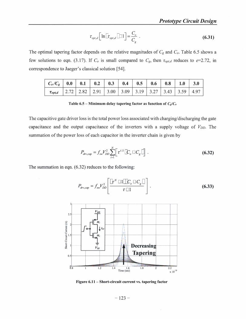
Prototype Circuit Design
Toptd In aot,d []]] C
g(6.31)
The optimal tapering factor depends on the relative magnitudes of Cg and C. Table 6.5 shows a
few solutions to eqn. (3.17). If C, is small compared to Cg, then Topt,d reduces to e=2.72, in
correspondence to Jaeger's classical solution [54].
Co/Cg 0.0 0.1 0.2 0.3 0.4 0.5 0.6 0.8 1.0 3.0
Toptd 2.72 2.82 2.91 3.00 3.09 3.19 3.27 3.43 3.59 4.97
Table 6.5 - Minimum delay tapering factor as function of Cg/Co
The capacitive gate driver loss is the total power loss associated with charging/discharging the gate
capacitance and the output capacitance of the inverters with a supply voltage of VDD. The
summation of the power loss of each capacitor in the inverter chain is given by
N n
drv,cap= sVD[oECg] (6.32)
The summation in eqn. (6.32) reduces to the following:
Idrv,cap = fswVDDr l ]L j1
(6.33)
Ic
M2IOVisc
0.8 1 1.2 1.4 1.6Time (see)
Tap ering~
5 -.1.8 2 2.2
x10.10
Figure 6.11 - Short-circuit current vs. tapering factor
- 123 -
2.5|
U
rj2
0.
3

Prototype Circuit Design
In addition to capacitive loss, there is also short circuit loss in the driver, which occurs when both
the PMOS and NMOS devices in the inverter are on at the same time. A plot illustrating the effect
the tapering factor has on the profile of short-circuit current is shown in Figure 6.11.
The short-circuit power loss in a tapered gate driver is the summation of the short-circuit power
loss in each inverter as given by
N te
Pd,sc = fSWVDD 1 ISCdt, (6.34)k=1 0
where Isc is the short-circuit current in the first inverter within the gate driver. The summation in
eqn. (6.34) reduces to the following:
WHL O(1 L b) W tn
Pdrv,sc = fSWVDD n Isc dt = fsWVDDQSC . (6.35)(z- LI1)(1 L b) K., )
As can be seen, Pr,sc is proportional to the total amount of charge Qsc that is lost when all the
PMOS and NMOS devices in the inverter chain are both on at the same time.
The total power loss in a gate driver is the summation of the capacitive loss and the short circuit
loss as given by
Pd = P,,,ca U Ps (6.36)
Next, we discuss how the tapering factor relates to the rise/fall time of the main driving power
MOSFET. A simplified diagram for the turn-on transition of the gate driver is shown in Figure
6.12 while the turn-off transition for the same driver is shown in Figure 6.17.
VDD VDD
IsaP,N
WM WM
T -esaNr MJNO
CMIsatNNV
Vss Vss
Figure 6.12 - Turn-on transition of the gate driver Figure 6.13 - Turn-off transition of the gate driver
-124-

Prototype Circuit Design
Based upon the simplified diagrams above, the summation of the rise time trise and the fall time tfall
can be calculated using
rise fall DDLTM C0 LU (6.37)_ satP,N 'satN,N j
The foregoing assumes
JsatP,N N1WIsatPO (6.38)
and
IsatN,N n satNO (6.39)
If we substitute eqns. (6.26), (6.29), (6.30), (6.38), and (6.39) into eqn. (6.37), then we obtain
tris E tfa = VDD riMO I lJbrECIpobEC I E 1 (6.40)_ satPO satN .
For example, if b=3, C0=0, and IsatPO=LatNO, then eqn. (6.40) can be simplified to
- [ '16) VDDCMO(
3 satNO
The strength of the gate driver determines the trise and tfall of the main power device it drives. If the
driver is too weak, then trise and tfall are high and the switching loss in the main power device is
large. However, if the driver is too strong, then the power loss in the driver is large. Thus, there is
an optimal gate driver strength set by the tapering factor for the minimum power loss.
6.4 Control Design
In the split-power architecture, the regulation stage controls the output voltage while the
transformation stage runs in open loop. As a result, the regulation stage requires a controller, which
determines the duty cycle of the power devices, such that the output voltage is regulated in spite
of variations at the input or output port of the power converter. To accomplish this task, the
controller must sense the output voltage either directly or indirectly. In some instances, it is also
desirable to measure other parameters, such as the inductor current or switch current. However, in
- 125 -

Prototype Circuit Design
this design, we settled on linear voltage-mode control because it is straightforward to design and
implement. In contrast, a more complex control technique, such as V2 control [37], could have
been used.
In our controller, the output voltage is compared with a reference voltage and the residual is
conditioned by a voltage compensator. The design of the voltage compensator sets the bandwidth
and steady-state accuracy of the control loop. The output of the compensator is a control signal ve,
which is fed into a pulse-width modulator. It is then compared with a triangular waveform, thereby
producing a double-ended PWM gate signals for the power stages. The PWM signal is further
conditioned by a dead-time control circuit. The circuit implementation of the controller needs a
triangular waveform generator, a pulse-width modulator, a dead time controller, and compensator.
Figure 6.14 illustrates a small-signal block diagram of the regulation stage along with the
controller. All of the small signal variables are lower case and denoted with a hat.
Buck i(Converter
V" (S) - + Gvg (s) + 9 (s)
( )s
Gc s) H -(s G(s)
Vref(S)
Figure 6.14 - Small-signal block diagram of the regulation stage
In the small signal model, the ac behavior of the Buck converter is represented by Gvg (s), Zo (s),
and Gvd (s). While, the voltage compensator's transfer function is H, (s) and the pulse-width
-126-

Prototype Circuit Design
modulator's transfer function is Gm (s). The response of the output voltage depends upon the duty
cycle D, the supply voltage V, to the Buck converter, and the output current Io. The small signal
ac response of the output voltage is given by
i,(s)= G, (s)d(s) W G, (s)^ (s) E Z (s)io . (6.42)
The variations in V and Io can be compensated for by modulating D, which is the purpose of the
controller.
In the case the input voltage perturbation is zero, the closed-loop output impedance can be
expressed as
S1 G(s - (6.43)10 1WE Gvd KWGLWJHII5E
This shows that there is a variation in the output voltage in response to a perturbation in the output
current. This effect can be minimized by having a fast control loop. It has also been shown in a
Buck converter that a voltage mode control scheme has a faster response to load variations than
current mode control due to the lower closed loop output impedance [102].
The closed-loop audio susceptibility (transfer function from buck converter input voltage to output
voltage) for the general case is
(6.44)v, 1L GvdEGG,,,sDHsE
assuming the output current perturbation 1 is zero. As can be seen, a variation on V, has the
potential to feed through the Buck converter on show up on the output voltage Vo. This effect can
be minimized if additional loops are added to the controller (e.g., feed forward control) or if the
control bandwidth of the regulation stage is much higher than the SC switching frequency as is the
case in this architecture.
In the remaining portion of this section, we discuss the design of the feedback path. Under voltage-
mode control, D to Vo transfer function of a Buck converter is given by
- 127 -

Prototype Circuit Design
V 3rEtCsGlG~dLsD- V1,D(6.45)
LCs 2 EV DcE s
or, in the case of Ridley et al. [91],
rrL E cta-lD El tr, 3 E D Er (6.46)
n,
The ESR of the output capacitor is re, the series resistance of the inductor is rL, the on-resistance
of the control switch is rctl, the on-resistance of the synchronous rectifier is rsr, and the number of
phases is n4.
The transfer function of the regulation stage designed in Section 6.2 can be found by substituting
the design parameters from Section 6.2 and operating point (V = 1.8 V, D = 0.556) into eqns.
(6.45) and (6.46), yielding
7.92 x10⁹s L1.8
2.904 x10 4 s 2 L 3.082 xI0]s .1(6.47)
The purpose of the pulse-width modulator is to produce a duty cycle that is proportional to analog
control signal v. It produces a logic signal, which commands the power converter switches to turn
on and off. The gain of the modulator is defined as
1G,. sV= , (6.48)
pk,saw
where Vpksaw is the peak ac voltage of the triangular waveform at the input of modulator. It should
also be pointed out that the pulse-width modulator samples v, with a sampling rate equal to the
switching frequencyfb2 of the Buck converter. Therefore, this simple dc model is only accurate
with frequencies less thanfb2/2 [87].
The function of the compensator is to stabilize and shape the feedback loop. It is always possible
to stabilize a loop by just decreasing the dc gain of the compensator until the crossover frequency
occurs at a frequency below the location of poles and zeroes from the reactive components in the
power stage. Therefore, the goal of a compensator is cross over at a high frequency with a good
phase margin.
- 128 -

Prototype Circuit Design
A compensator sets the bandwidth and steady-state accuracy of the control loop. It is traditionally
implemented using an error amplifier in an inverting configuration with two complex impedances
Zi and Z2 as shown in Figure 6.15. These impedances are typically realized using capacitors and
resistors; however, inductors would work as well. Different configurations of these components
are chosen depending upon the phase boost needed for the desired phase margin. In addition, to
prevent loading down the error amplifier, the capacitor values should be small while the resistor
values should be large.
Z2
IN Z1 -OUT
VREF -+#
Figure 6.15 - Simplified compensator with compleximpedances Zi and Z2
C2
R3 C3
-WV-dR2 C1
R,IN -
-- OUTVREF- c
s
Figure 6.16 - Type-3 compensator schematic
In order to respond to large slew rates imposed by digital logic, the prototype power converter
must have either a large control bandwidth or a large amount of output capacitance. Since the goal
of this design is to create a high power density design, we have chosen to push up the control
bandwidth instead. Therefore, to be on the safe side, the power converter's control loop was
designed to be closed at 1/5 offb2 (6 MHz) with a 60 degree phase margin.
The compensator's transfer function is designed using eqns. (6.45) through (6.48). Normally, the
loop is closed at a frequency above the power stage's resonance frequency. Quite a bit of phase
boost was required to stabilize the loop so a type-3 compensator as depicted in Figure 6.16 was
chosen with a transfer function of
Li D s / co t 1E S / CQ z
S []s / C0,1 O E s / CO, 2 E(6.49)
In designing the compensator, the two zeroes ozi and Oz2 were used to cancel out the double
resonant poles of the regulation stage, while the two poles copi and Op2 were used to cancel the
-129-

Prototype Circuit Design
zero from the ESR of the output capacitor Co. Finally, the desired crossover frequency is set by
adjusting the dc gain K, [102].
The voltage loop gain T(s) defined as
T 5 []- G [Gm 5 OHE, 5. (6.50)
Figure 6.17 illustrates a plot of the small signal closed loop response when V, is equal 1.8 V and
the Vo is equal to 1.0 V.
CU
1008060 -
40200
-20-40-60-80
-1000
-20-40-60-80
-100-120-140-160 -
-180 -
.E+05 1.E+06 1.E+07 1.E+08Frequency (Hz)
Figure 6.17 - Small signal closed loop response of the controller
1.E+09
In order to achieve this type of loop response, the compensator's transfer function is
9ls /6.37x10 6 L s /6.37x10 6R
s H ( s /203.7 x106 lJs /203.7 x106D
This transfer function corresponds to the component values in Table 6.6.
(6.51)
- 130-
'11............. ... .. .... ....

Prototype Circuit Design
Capacitors Value Resistors Value
C1 1394 fF R1 100.0 kQ
C2 45.0 fF R2 112.6 kg
C3 1520 fF R3 3.23 kQ
Table 6.6 - Compensator component values
As can be seen from the bode plot, the loop is stable. We are able to achieve the target 6 MHz
crossover frequency with a 60 degree phase margin. The control loop could have been pushed even
higher, but would have been more susceptible to noise. Nevertheless, the selected control
bandwidth is much higher than a typical converter of this voltage and power range. This allows
this prototype design to respond to a large slew rate in output current without requiring large
amount of bulk output capacitance. This is one of the main benefits of the high frequency
operation.
In this design, the target crossover frequency was quite high so we had to design a high-
performance error amplifier with very high frequency internal poles and zeroes that would not
interfere with the poles and zeroes added externally. This is a less than elegant solution, but quite
effective. Additionally, the error amplifier needed a moderate gain so that the compensator's gain
did not vary a significant amount over process variation. This made the design of the error
amplifier a little more challenging. The dc gain Av,dc of the compensator sets the steady-state output
voltage error A V0 ,dc of the power converter, which is given by
AV, d, - o - (6.52)
In this design, a compensator gain of 222 V/V was required to achieve a steady-state output voltage
error A V,dc of ImV for an output voltage Vo of 1.0 V, if Vx=1.8 V and Gm=2.5 V.
After the compensator was completed, a transient simulation was run to check loop stability in the
time domain. Figure 6.18 shows the simulated output voltage response to a step-down current
transient. The current step goes from 2.0 A to 0.2 A within 1.0 ns. The step-down response has a
voltage overshoot of approximately 66.3 mV and returns to its desire output voltage in 200 ns. It
- 131 -

Prototype Circuit Design
has a state-state voltage error of 1.0 mV. The target specification was to keep the output voltage
deviation within 10% of the normal voltage, which in this case it met.
0
0
1.081.071.061.051.04
1.031.02
1.011.000.990.98
2.50
2.00
1.50 *
1.00
0.50 0
-Vout (V)
-lout (A)
0.2 0.3 0.4 0.5 0.6
Time (ps)
0.7 0.8 0.9 1.0
Figure 6.18 - Simulated transient step response of the prototype power converter
6.5 Overall System Design
Now that we have discussed the design of the transformation stage, regulation stage, and the other
major blocks, it is time to put everything together. The total device area of both stages combined
is 2.372 mm 2 . However, after layout, the die area increased to 8.462 mm 2 . The die was actually
enlarged on purpose to allow the power devices to align directly underneath their respective energy
storage elements. The extra silicon area is filled with on-die capacitors and ESD structures.
The total efficiency of the prototype power converter is given by
7 tot = 7, X 7462 , (6.53)
where the efficiency 7se of the switched capacitor stage is given by eqn. (6.7) and the efficiency
77b2 of the Buck converter stage is given by eqn. (6.21). Figure 6.19 shows a plot of the simulated
total efficiency tot of the prototype converter versus output current. There are six curves in the
Figure 6.19. The bottom three curves are for the prototype power converter at three different input
voltages. In contrast, the top three curves in the graph are for another power converter design that
utilizes a more advanced switched capacitor transformation stage. All of these curves correspond
to when the power converter has an output voltage of 1.0 V.
- 132 -
0.00

Prototype Circuit Design
100.00-4-9Vin=5.5
-*-Vin=4.5
96.00 -+-Vin=3.5
94.00
1 92.00
0 90.00
88.00 ____
86.00
84.00
82.00
80.000.00 0.50 1.00 1.50 2.00
Output Current (A)
Figure 6.19 - Efficiency vs. load of the prototype power converter
The transformation stage and regulation were optimized in isolation. It was the objective to split
the power loss equally between the transformation and regulation stage. Unfortunately, this is not
possible when there is a large variation in supply voltage. Figure 6.20 shows a breakdown of the
power loss for the prototype converter. This data corresponds to when the converter has an output
voltage of 1.0 V and output power of 2.0 W. Within the plot, the switched capacitor loss is denoted
by resSC and gateSC. All of the other loss mechanisms are associated with the Buck converter. As
can be seen figure, the transformation stage and regulation stage only have similar losses at a
supply voltage of 5.4 V.
0.45 *resSC
0.4 EgateSC*resLEresH
0.35- EgateLgateH
0.3- MoutLHoutH
-0.25- EwellL[drvL
( 0.2- *drvH*dcnd
Uclnd0.15 _acInd0coreInd
0.1 -bump
0.05- -
.05 3. Input Voltage .
Figure 6.20 - Power loss breakdown of the prototype power converter
- 133 -

Prototype Circuit Design
The SC converter consumes a larger percentage of the power loss as the input voltage lowers,
which is due to the increased on-resistance of M3, M4 , M6 , and M7. The sources of these devices
are connected to internal nodes within the SC network so their gate to source voltage is always
less than the input voltage; this is especially true for M4. Even considering this shortcoming, the
efficiency of the prototype converter is always above 80% - see Figure 6.19. This level of
efficiency is in line with the state-of-the-art power converters.
Component Total Volume
IC 1.69 mm3
Cin 0.25 mm 3
CJ-3 0.75 mm 3
CX 0.25 mm3
L 0.72 mm3
CO 0.11 mm3
Table 6.7 - Volume of the components in prototype power converter
However, the power density is what really sets the prototype converter apart from its competition,
which we now discuss. The prototype power converter has a total component volume of 3.77 mm3,
yielding a component power density of 0.530 W/mm3 . Table 6.7 shows the volume of each major
component in the design. As before, we are assuming that the thickness of the silicon die is 200 pim
and the inductor is the 33 nH foil-wound inductor as described in Appendix D. It is also important
to note that the power density calculation and the two previous power density calculations only
take into account the volume occupied by each component. They do not take into account all the
additional space required after packaging.
In summary, a prototype converter was designed for an input voltage range of 2.7 V to 5.5 V and
output voltage of less than 1.2 V with a maximum output power of 2.4 W. It utilizes a new power
converter architecture that combines the strengths of switched capacitor converters with the assets
of switch-mode power converters.
-134-

Chapter 7 - Prototype Package Design
In power electronics, packaging is often one of the most critical aspects to achieving high power
density. As power density increases, a larger amount of power is processed in a smaller space. This
can lead to both electrical and thermal issues that need to be managed. As a result, we developed
an advanced packaging scheme that enabled us to achieve both a high power density and excellent
electrical performance. The goal of the package was to create a self-contained power converter
module that did not require any external passive components. The resulting module could then be
soldered directly onto a standard PCB. Figure 7.1 shows a block diagram of the IC (also known as
a die) within the package.
Vss
Isc
VDUTY
VD0
VOG
'BIUS
Vs
J/SS
IBUCK
VREF
VERM2
VSEL VENSC VESEL
Figure 7.1 - Block diagram of the IC within the package
The prototype IC described in Chapter 6 is the heart of the power converter module. Figure 7.2
shows the first version of the fabricated IC. The package connects the pads on the IC to the outside
world and to the necessary passive storage elements (e.g., capacitors and inductors). In the initial
- 135 -

Prototype Package Design
version of the IC, there are 476 pins in a 14 x 34 array and each pin has a 50 pm pad opening with
a pitch of 110 tm.
Figure 7.2 - Image of the fabricated prototype IC (Vs version)
Unfortunately, the tight pitch of the first version of the prototype IC made it extremely challenging
to package, as discussed in Section 7.2. Therefore, we designed and fabricated a second version of
the IC with a relaxed bump pitch as illustrated in Figure 7.3.
Figure 7.3 - Image of the fabricated prototype IC (2nd version)
The pad pitch expanded from 110 pim to 220 pm and the pad opening expanded from 50 ptm to
125 pm. As a result, the number of pins decreased by 3.3 times. Figure 7.4 illustrates a pin out for
the second version of the prototype IC.
-136-

Prototype Package Design
ORIGIN 01 02 03 04 05 06 07 08 09 10 11 12 13 14 15 16 17 18
C VM
B
A
Figure 7.4 - Pin out for the 2 n version of the prototype IC
This version of the IC has 144 pins and Table 7.1 illustrates a description of each pin. Of the 144
pins, 133 are used for power while the remaining 11 are used for control.
Name Type Comment
VIN Power input voltage railVO Power output voltage railVSS Power ground railV1 - V4 Power internal SC nodesVX Power intermediate voltage nodeVM Power inductor nodeVDD Power supply rail for control circuitryVBG Analog 1.25 V voltage referenceVREF Analog output voltage referenceVFB Analog feedback nodeVDUTY Analog controls SC duty cycleIBIAS Analog 500 nA current biasIBUCK Analog controls buck frequencyISC Analog controls SC frequencyEN SC Digital enables SC converterEN BK Digital enables Buck converterVSEL Digital selects SC ratio (2:1 or 3:1)ESEL Digital enables feedback loop
Table 7.1 - Pin description for the 2 nd version of the prototype IC
Great care was taken in laying out the components (i.e., power MOSFETs) in the IC to reduce the
series resistance and inductance. In general, ICs have relatively thin metal layers as compared to
PCBs. The processes used to create multiple wiring layers are fundamentally different between
-137-

Prototype Package Design
ICs and PCBs. To reduce the impact of metal thickness on the interconnect resistance, we used the
metal lines on the IC for routing current in between bumps and the metal lines on the PCB for
routing between bumps, resulting in a large number of power pins. A few techniques to model the
interconnect loss are shown in Appendix F.
The remainder of this chapter focuses on the methods used to package the prototype ICs.
7.1 Package Design
In the 1960s, the semiconductor industry explored various methods of connecting a semiconductor
die to external components. This period coincided with the introduction of the silicon IC. In
general, three basic interconnect approaches were developed: wire bonding, tape automated
bonding, and direct chip connections. All of these can be used to connect a semiconductor IC to
an electrical interface, such as a PCB, lead frame, substrate, and so on. Five decades later, we are
still using the same three basic interconnect approaches, but with more variations and
enhancements.
Wire bonding, first introduced by Bell Laboratories in 1957, is the earliest of the three
semiconductor joining technologies [5]. In this process, soft metal wires are joined to a face-up
semiconductor die through a solid-state metallurgical interaction. Figure 7.5 illustrates a packaged
IC using wire bonds. One by one, each wire is bonded to the IC and then to the package using
either ultrasonic bonding, thermocompression bonding, or thermosonic bonding. Wire bonding is
generally considered the most cost effective and flexible interconnect method. Therefore, the
majority of ICs are packaged using this technology.
Package wire Bond
rizm 4AllzIt Cir1it C2oar
Printed Circuit Board
Figure 7.5 - Cross section of a wire bonded package
Unfortunately, wire bonding is less than an ideal connection. For example, a 1.0 mm long gold
bond wire with a diameter of 1.3 mils has a resistance of 25.7 mK2. To put this into context, a single
power FET in our transformation stage has an on-resistance of 13.4 mQ. Numerous wire bonds
- 138-

Prototype Package Design
would have to be used in parallel to reduce the resistance to an acceptable limit. The large number
of connections for the transformation stage makes this impracticable for our design.
The tape automated bonding (TAB) approach solves the sequential nature of wire bonding. The
beam-lead structure was an early precursor to the TAB structure [63]. General Electric further
developed the concept in the 1960s with the development of their mini mod process, which is
arguably the first TAB process [4]. In this process, a semiconductor IC is joined to patterned metal
foil on polymer tape in a single operation using thermocompression bonding. The patterned metal
tape serves the same function as the bond wires, therefore TAB has similar electrical limitations
to wire bonding.
To reduce the resistance of the electrical connections, a more direct approach is required. IBM
developed such a technique in 1961. In the direct chip connection, the semiconductor die is joined
face down on the printed circuit board [62]. Small conductive bumps, typically deposited on the
IC, provide the electrical connections. This technique is also referred to as flip chip due to the
orientation of the die.
MLCC Foil Inductor Package
Laminate
Power In " Power Out
Standard PCB (20 mihs
Figure 7.6 - Cross section of an initial power converter module
During the assembly process of our prototype module, we developed a few different package
incarnations. Each power converter module was composed of three main components: a silicon
die, a high-density interconnect (HDI) laminate, and passive components. The laminate, along with
the conductive bumps, provides the electrical connections between the passive components and
the silicon IC. Figure 7.6 illustrates a cross sectional view of one of the initial power converter
modules.
-139-
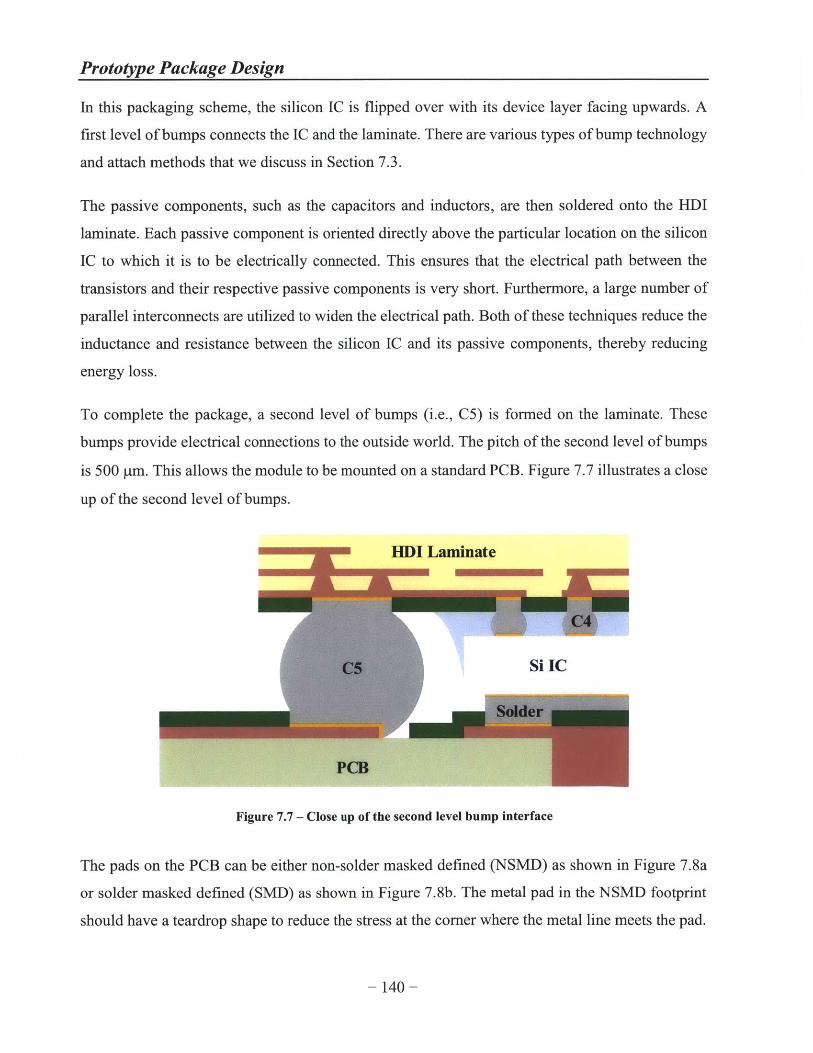
Prototype Package Design
In this packaging scheme, the silicon IC is flipped over with its device layer facing upwards. A
first level of bumps connects the IC and the laminate. There are various types of bump technology
and attach methods that we discuss in Section 7.3.
The passive components, such as the capacitors and inductors, are then soldered onto the HDI
laminate. Each passive component is oriented directly above the particular location on the silicon
IC to which it is to be electrically connected. This ensures that the electrical path between the
transistors and their respective passive components is very short. Furthermore, a large number of
parallel interconnects are utilized to widen the electrical path. Both of these techniques reduce the
inductance and resistance between the silicon IC and its passive components, thereby reducing
energy loss.
To complete the package, a second level of bumps (i.e., C5) is formed on the laminate. These
bumps provide electrical connections to the outside world. The pitch of the second level of bumps
is 500 ptm. This allows the module to be mounted on a standard PCB. Figure 7.7 illustrates a close
up of the second level of bumps.
HDI Laminate
Si IC
Figure 7.7 - Close up of the second level bump interface
The pads on the PCB can be either non-solder masked defined (NSMD) as shown in Figure 7.8a
or solder masked defined (SMD) as shown in Figure 7.8b. The metal pad in the NSMD footprint
should have a teardrop shape to reduce the stress at the corner where the metal line meets the pad.
-140-

Prototype Package Design
(a) NSMD (b) SMD
Figure 7.8 - NSMD and SMD PCB pad layouts
Typically, NSMD pads are preferred when the bump pitch is larger than 400 ptm because metal
layers have a smaller registration tolerance than solder mask layers in a PCB process. However, if
the pitch is smaller than 400 pm, it is typically not possible to utilize NSMD pads because the
solder mask dam within the bump array will be too thin.
7.2 HDI Laminate Design
The HDI laminate within the package provides the electrical interface between the silicon IC and
its respective components. It also provides a low impedance path to connect the large power
transistors in the power stage. The on-die metal is 1.0 ptm of aluminum, so the thick copper traces
on the laminate are effective in shunting the current through the laminate instead of on the IC.
Both versions of the prototype IC have very small bump pitches, so the requirements for the
laminate are very stringent. Creating a laminate that balanced electrical performance and ease of
fabrication was the most challenging aspect of the package design.
In general, a HDI PCB is a PCB with a higher wiring density per unit area than a conventional
PCB and characterized by high-density attributes including laser micro vias, fine lines/spaces, and
high-performance materials. Laminate is another name for a PCB because the layers within a PCB
are joined together using a lamination process. For the purpose of the thesis, we will refer to the
PCB within the package as a laminate.
- 141 -

Prototype Package Design
A distinguishing characteristic of any HDI PCB is a thin build-up layer with micro-vias providing
the electrical connection between build-up layers. A micro-via is defined by the IPC as any via
with a diameter less than 150 ptm. There are several methods of producing micro-vias, which
include laser ablation, plasma etching, photo imaging, and mechanical drilling. Each method has
its own benefits and drawbacks, but laser ablation is currently the most popular method. Depending
upon the process, micro-vias on different layers can be either staggered or stacked. Additionally,
the micro-vias can be filled with copper or conductive paste.
There are numerous types of HDI PCB structures and two common ones are shown below.
Figure 7.9 - Cross section of a HDI PCB with a core
Figure 7.10 - Cross section of a coreless HDI PCB
Figure 7.9 illustrates the simplest HDI PCB structure. In this example, there is a center core with
build-up layers on both sides. Build-up layers are typically applied to opposing sides to balance
thermal and/or mechanical induced stresses. The center core is usually manufactured using
conventional PCB techniques. Therefore, the vias in the center core are mechanically drilled and
have a large diameter. As a result, the center core is a potential wire density bottleneck.
In contrast, the HDI PCB structure in Figure 7.10 does not have a center core. It is fabricated only
with build-up layers, each of which can be rigid or flexible. This type of construction allows for a
very high density of interconnections while also providing a very low profile solution. This type
of structure is typically the most expensive solution as well.
- 142 -

Prototype Package Design
For the first prototype IC, a four-layer coreless HDI laminate with flexible layers was constructed
using a subtractive process. Figure 7.11 shows a layout of the HDI laminate. The minimum feature
size of the laminate was 30 pm with 25 pm stacked vias, which is barely sufficient to route the IC.
To fabricate such small features, the outer metal layer thickness was quite thin. In this case, it was
12 pm, which correlates to approximately "1/3 ounce copper". The interlayer dielectric is
polyimide and the board has a total height of 250 gm.
Figure 7.11 - Layout of the HDI laminate for the first prototype IC
The processing of the HDI laminate starts with a 25 pm thick polyimide base material with 5 pm
of electrodeposited copper. The vias from L2 to L3 are formed using laser drilling. The inner walls
of the vias are first coated with a semiconducting tin/palladium layer and then electroplated with
copper, resulting in a metal thickness of 12 pm for L2 and L3. After the plating process, L2 and
L3 are patterned and chemically etched.
The resulting core structure is then sandwiched between two resin-coated-foil (RCF) films. Only
one lamination cycle is required, as this limits the amount of material movement that accompanies
every lamination cycle. The blind vias from Li and L4 are then laser drilled and electroplated.
Last, the traces on Li and L4 are patterned and chemically etched.
To finish off the HDI laminate, a 25 pm thick liquid photoimageable solder mask is applied to the
top and bottom of the laminate. Laser ablation creates pad openings in the solder mask. The pads
are then finished with electroless nickel immersion gold (ENIG).
Figure 7.12 illustrates a cross section of the fabricated HDI laminate. As can be seen, there are
opens in the vias. The laminate was designed with a large number of parallel vias and wires, so
- 143 -

Prototype Package Design
these opens will only cause a drop in efficiency. Unfortunately, there are metal shorts in the
laminate as well and the design cannot tolerate this type of defect.
L4
L3
L2
Figure 7.12 - Cross section of the HDI laminate for the first prototype IC
After numerous attempts, we were unable to obtain a functional HDI laminate that met our
electrical specifications. Therefore, to test the functionality of our IC, we wired bonded our
prototype chip directly onto a specially designed measurement board with a 99% soft gold surface
finish, as illustrated in Figure 7.13. Fortunately, our ICs come from the fab without any solder
balls. Additionally, the top metallization is aluminum so the pads are wire-bondable.
Figure 7.13 - Top view of the first prototype IC after wire bonding
Initially, it was very difficult to form a good joint between the bond wire and the aluminum pad
using a gold wire ball bonder because of the small pad opening (i.e., 50 pm). As a result, we used
-144-

Prototype Package Design
an aluminum wedge bonder to complete the task. Figure 7.13 illustrates a top view of the wire
bonded IC, while Figure 7.14 illustrates an isometric view. With the assistance and use of facilities
at the Charles Stark Draper Laboratory, it took half a day to complete a single chip, which required
108 wire bonds. After successfully wire bonding the IC, we assembled the measurement board and
discovered that the IC was functional. Consequently, we designed and fabricated a second
prototype IC with a wider bump pitch of 220 pm.
Figure 7.14 - Isometric view of the first prototype IC after wire bonding
For the second IC, Sierra Circuits in Sunnyvale, CA, fabricated a less-aggressive four-layer
coreless HDI laminate with rigid glass reinforced layers using a semi-additive process. The
minimum feature size of the laminate was relaxed to 50 pm and the vias were enlarged to 75 pm.
Furthermore, to improve their reliability, the vias were copper-filled and staggered. The metal was
also thicker; each layer had a final metal thickness of approximately 25 pm. Figure 7.15 illustrates
a cross section of the laminate with a height of approximately 250 pm.
L4
L3
L2
Li
Figure 7.15 - Stack-up of the HDI laminate for the second prototype IC
- 145 -

Prototype Package Design
Figure 7.16 shows the top side of the laminate, while Figure 7.17 shows the bottom side of the
laminate. In both figures, the pads are labeled with their pin name, excluding the ball grid array
(BGA) for the IC.
Figure 7.16 - Top side of HDI Laminate with pin name overlay
Figure 7.17 - Bottom side of HDI laminate with pin name overlay
To improve the chance of a successful build, Sierra Circuits selected a board material that was low
in glass, high in resin, and resisted wicking. They adjusted the plating chemistry and current to
match the plating requirements for the microvias. In addition to this, they measured the copper
thickness on the surface and in the holes at several steps. The laser drill process parameters were
also carefully adjusted for tight tolerances so that there were no tangential breakouts. Finally, the
ENEPIG surface finish chemistry was adjusted to make sure that the surface finish was flat on the
wire bondable pads and traces.
- 146-

Prototype Package Design
Aside from not meeting the line/space requirements, the previous laminate (110 Im pitch) had a
few flaws. It was very flexible due to the lack of a rigid board construction and the vias were not
filled, making it nearly impossible to mount the IC.
7.3 Direct Attach Methods
There are two levels of bumps in our package design. The first level of bumps is very small and
tightly packed, whereas the second level of bumps is much larger and loosely packed. This
therefore requires different bump technology and joining methods for each level of bumps. In this
section, we discuss the various flip chip technologies explored during the package design.
Material Method Process Die Level Attach Method
Solder Deposition Evaporation NO Reflow + underfill
Plating Electro NO
Electroless YES
Ball Solder ball YEStransfer YES
Solder jetScreen Solder paste YESPrinting deposition
Gold Ball Stud bump NO Conductive paste + underfill
Plating Electro YES Reflow + underfillor Anisotropic conductive film (ACF)
Thermocompression + underfill
Copper Thermosonic + underfillPressure contact + non-conductive paste
Table 7.2 - Summary of commercially available bumping processes
In general, the joining processes developed by the semiconductor industry can be classified into
two main categories - dry and wet processes. The dry processes take the form of solid-state
metallurgical interactions, such as ultrasonic, thermocompression, or thermosonic bonding. The
wet processes are represented by solders and adhesives. Additionally, some joining processes
utilize a combination of dry and wet processes. Table 7.2 illustrates a comprehensive list of
commercially available bumping processes.
IBM introduced the earliest form of flip chip technology; they used solderable metal balls as the
electrical interconnect [32]. Rigid copper spheres supported the semiconductor die during the
reflow process. A few years later, it was realized that the copper spheres could be removed if the
- 147 -

Prototype Package Design
pads on both surfaces to be joined were designed to restrict solder wetting. By limiting the
solderable areas, the surface tension of the solder in its molten state provided support during
reflow, thus preventing its collapse. This technique was referred to as a controlled collapse chip
connection, or C4 in abbreviation [73].
There are numerous methods of creating solder bumps. In the early days, IBM evaporated solder
through a shadow mask. Over time, less expensive processes have been developed, such as screen-
printing [58]. In this process, a metal stencil is aligned with the pads on the die, solder paste is
applied, and a squeegees is rolled across the metal stencil to distribute the solder paste evenly. A
solder paste pattern is left behind after the stencil is lifted. The dies then go into an oven where the
solder solidifies into spheres. Figure 7.18 illustrates an array of solder bumps after reflow with a
diameter of 125 pim. If you look carefully, the solder bumps are non-uniform. In this instance, flux
was not applied during the reflow process, thereby elongating the solder bumps to prevent solder
bridging during the attach process. (CVInc in Rowlett, TX, carried out the solder bumping)
Figure 7.18 - Side view of a solder bump array
Screen-printing is an efficient method when the bump array is large. However, if there are only a
few bumps, then placing pre-formed solder balls by hand is also practical. This method is very
straightforward. We first apply flux to the target pad, position a pre-formed solder ball, reflow the
solder ball, and then repeat the process on the next pad. This was our primary method of placing
the second level of bumps.
- 148 -

Prototype Package Design
Instead of using solder to form the bumps, a metal such as gold or copper can be used to form the
bumps. There are a few different methods of creating the metal bumps. Ironically, a popular
method is to use a wire bonder. In conventional ball bonding, the tip of the bond wire is melted to
form a sphere. The wire bonder then presses this sphere against the bond pad. A metallic
connection is formed through the application of force, heat, and ultrasonic energy. To complete
the connection, the wire bonder would extend the bond wire to the connection pad on the PCB,
lead frame, substrate, and so forth. However, instead of finishing the connection, the wire bonder
can shear the bond wire close to the ball, forming a metal bump also known as a stud. To provide
a more uniform bump height, the studs can be flattened afterwards. Figure 7.19 illustrates a top
view of 3.0 mil gold stud bumps in a 220 pm pitch array.
Figure 7.19 - Top view of a gold stud bump array
Once the metal studs are formed, there are numerous methods of joining the opposing side of the
stud in which either a wet or dry joining process is used. Logically, the same process that formed
the metal stud in the first place can be repeated to finish the joint - in this case, either ultrasonic,
thermocompression, or thermosonic bonding. These processes provide a very good electrical
connection; however, there is very little room for error. For these processes to be effective, all of
the studs need to have similar heights and the opposing surface needs to be flat and rigid. As
illustrated in Figure 7.20, gold studs can be planarized using a "coining" process.
There are a few different variations of the wet joining process, which are either solder or adhesive
based. The adhesives can be either conductive or non-conductive. There are two main types of
-149-

Prototype Package Design
conductive adhesives: anisotropic conductive adhesive (ACA) and isotropic conductive adhesive
(ICA). All electrically-conductive adhesives consist of conductive fillers in a polymer binder.
ACAs are only electrically conductive in the vertical or Z-axis, whereas ICAs are electrically
conductive in all directions. The conductive filler loading factor determines the type of adhesive.
Figure 7.20 - Side view of a gold stud bump array after the coining process
In ACAs, the loading factor is sufficiently low such that there is no inter-particle contact.
Conductivity can be achieved by applying both heat and pressure. After curing, the material only
conducts in the direction pressure was applied. In contrast, ICAs have a higher loading factor of
approximately 25-30 volume percent. At these levels, the material is above the percolation
threshold, so it is electrically conductive in all directions [117]. The most popular ICAs are silver
flaked filled thermosetting epoxies. Figure 7.25 illustrates a gold stud attached to a pad with this
type of adhesive.
As previously stated, the gold studs can be joined using solder. Care must be taken when selecting
the type of solder. Tin readily dissolves gold during reflow, and therefore tin-bearing solder such
as Sn63/Pb37 solder must be avoided [1]. Solders that replace the tin with indium are a good
alternative because the dissolution rate of gold in indium is much slower. A few common choices
of indium-bearing solder are In70/Pb3O and In97/Ag3, the latter of which we tried during our
assembly process.
-150-

Prototype Package Design
7.4 Final Assembly
In this section, we discuss the assembly of the power converter module that is tested in Chapter 8.
As depicted in Figure 7.21, the assembly process can be broken up into seven separate steps and
Figure 7.22 illustrates a cross section of the resulting module.
From Foundry
Thin Silicon Die
Apply UBM to Die
Bump Die
Attach Die to Substrate
0 Apply Underfill
GAttach Passives to Substrate
Bump Substrate
To PCB
Figure 7.21 - Module assembly Figure 7.22 - Cross section of the power converter moduleprocess flow
The assembly process starts with thinning of the dice. When the dice come from the foundry, they
are 725 gm thick and need to be thinned down to 200 pm. This is accomplished by back grinding,
which is done at Aptek Industries Incorporated. The front surfaces of the dice are held down
utilizing a wax mount, and downward pressure is applied as the backside is ground. In between
the die and mounting plate, there is wax and an ultra-thin laboratory paper that protects the top
side of the die from scratches or other damage.
Figure 7.23 shows an image of the die thinned down to 60 pim. The die warps because the high
density of metal on the top surface induces stress that warps the die. The die would be able to
retain its shape in spite of the stress generated by the top metal if the die were thicker.
- 151 -

Prototype Package Design
Figure 7.23 - Side view of the die when thinned to 60 pm
After thinning, an under bump metallization (UBM) layer is applied to the pads prior to bumping.
The UBM serves two distinct purposes: it provides a solderable layer for solder bumps and/or
protects the multi-layer interconnect structure under the pad if gold studs are attached using a wire
bonder. We chose an electroless nickel, electroless palladium, immersion gold (ENEPIG) UBM
because it is both solderable and wire bondable. The nickel layer is 120 - 240 pin, the palladium
layer is 2 - 4 pin, and the gold layer is 1 - 2 pin.
Figure 7.24 illustrates a close up of the pads after the application of the ENEPIG UBM. The small
dot in each pad is a result of an incomplete top passivation etch at the fab. A small amount of
silicon nitride was on the pad prior to the application of the UBM; this had little or no effect on
the quality of the joint between the pad and the bump to be applied.
Figure 7.24 - Pad array after application of an under bump metallization
The dice are bumped after application of the UBM. During our packaging exploration, we tried
several of the joining methods described in Section 7.3. We tried solder balls that we deposited by
- 152 -

Prototype Package Design
both solder ball transfer and screen-printing. We also experimented with gold stud bumping and
various attach methods, which included thermocompression bonding, conductive epoxy, and
indium based solder. The various experiments were carried out with the assistance and use of
facilities at the MIT Lincoln Laboratory.
Of all the attach methods, gold stud bumping with conductive epoxy was the most effective, so
this was the method used in the tested prototype converter. The other methods had the following
challenges. The solder balls were difficult to work with due to uniformity issues; the gold stud
bumps with thermocompression bonding did not produce reliable joints because the laminate was
too flexible; and the gold stud bumps with indium-based solder had a limited working temperature
and number of reflow cycles.
Each gold stud on the die is coated with a uniform amount of silver epoxy by placing the die onto
a glass slide with a 1.0 mil thick layer of epoxy. Then, the gold studs are aligned with the pads on
the laminate and joined together by curing the epoxy in an oven. Figure 7.25 illustrates a side view
of a single gold stud attached to the laminate using conductive silver epoxy. Next, underfill is
applied between the laminate and die to protect the gold stud joints as the module goes through
the subsequent assembly steps.
Gold Stud
gr
Figure 7.25 - Side view of a gold stud attached with conductive silver epoxy
- 153 -

Prototype Package Design
The passive components are then attached to the laminate using either a soldering iron or solder
paste and a hot air gun. To finish off the power converter module, the second level of bumps (C5)
is attached to the laminate using the ball transfer process described in Section 7.3. The pre-formed
solder balls have Sn63/Pb37 composition with a diameter of 300 tm.
The laminate was designed with the foil-wound inductor in mind. Unfortunately, we did not have
the time to fabricate the foil inductor described in Appendix D. Therefore, we used off the shelf
magnetic-core inductors from Coilcraft. Figure 7.26 illustrates a close up of the module with three
Coilcraft inductors (PFL1005-101MRU) in parallel. To prevent damaging the IC during testing,
we decided to place the Coilcraft inductors off to the side of the laminate. However, there is
adequate space to place the inductors on top of the laminate.
Figure 7.26 - Top view of the completed prototype module
Figure 7.27 illustrates a cross section of the completed prototype module (inductors not shown).
Figure 7.27 - Cross section of the completed prototype module
-154-

Prototype Package Design
After some fine-tuning, it was found that the optimal energy storage capacitors Ci through C3 in
the transformation stage are 6.3 V, 10 pF MLCCs from TDK Corporation. Table 7.3 shows the
bill of materials for the prototype module. As it so happens, the components are slightly different
from those selected in Chapter 6.
Part Number
C1005X5ROJ106MO50BC
C1005X5ROJ106MO50BC
C1005X5ROJ106MO50BC
C1005X5ROJ106MO50BC
LG126Z104MAT2S1
JMK063BJ224MP-F
PFL1005-1OMRU
MITDGOO1
Count
2
1
1
1
1
1
3
1
Total
Volume (mm 3)0.50
0.25
0.25
0.25
0.25
0.06
1.54
2.15
5.25
Table 7.3 - Bill of materials for the prototype module
The prototype module is quite small - it has a width of 6.96 mm, a length of 2.56 mm, and a height
of 1.0 mm thereby yielding a footprint of 17.80 mm2 and a total volume of 17.80 mm3 . Based upon
the table above, the components consume 29.5% of the total package. Consequently, to improve
the power density further, the components could be packed closer together, thereby reducing the
wasted space.
- 155 -
Component
Cin
CI
C2
C3
CxCoL
IC

Chapter 8 - Prototype Measurements
In this chapter, we first discuss the measurement setup and then explain the procedures used to
measure the power converter module. Next, we show the measured results. Last, we place the
performance in context by comparing it with commercially-available modules and academic
works.
8.1 Measurement Setup
During the design process, we built a few hooks into the prototype IC allowing for optimization
after assembly. For example, the transformation stage and the regulation stage can be run
separately or together; likewise, the feedback loop within the regulation stage can be broken or
overridden. A simple digital bus controls both of the previous scenarios. Figure 8.1 illustrates a
top view of the measurement PCB, which includes bias circuitry, power supplies, digital inputs,
and a load. Details for this board are provided in Appendix G.2.
Figure 8.1 - Top view of the assembled measurement PCB
The measurement PCB is a four-layer 4.8" x 3.4" PCB with standard design rules. The top layer
is used to route power and ground for the power converter module while the bottom layer is mainly
-156-

Prototype Measurements
unused. The inner layers route a 5.0 V rail powering all of the ICs on the measurement PCB
excluding the device under test (i.e., the power converter module). A group of single pole, double
throw (SPDT) switches connected to a 1.8 V linear regular generate the digital inputs.
The bias circuitry consists of three current sources and three voltage sources that generate the
appropriate bias currents and bias voltages. The first bias current controls the switching frequency
of the regulation stage, the second bias current controls the switching frequency of the
transformation stage, and the third bias current is the master current source for all of the analog
blocks within the IC. Additionally, the first bias voltage controls the output voltage, the second
bias voltage controls the duty cycle of the transformation stage, and the third bias voltage overrides
the output of the error amplifier.
Instead of soldering each power converter module to the measurement board, we designed and
fabricated a small daughter board on which we mounted the power converter module. Figure 8.2
illustrates how the daughter board attaches to the measurement PCB. A pair of high-density sockets
on the daughter board snap together with a matching pair on the measurement PCB. This setup
allowed us to assemble power converter modules with different configurations without having to
alter the measurement PCB. Full details of the daughter board are included in Appendix G. 1.
Module
1Q1
Menurement PCB
Figure 8.2 - Side view of the measurement PCB and daughter board
Figure 8.3 shows the top and bottom views of the daughter board without a power converter
module mounted. On the top of the daughter board, there is space for input and output filter
capacitors. Furthermore, the daughter board has an exposed paddle on the bottom allowing heat to
transfer from the daughter board to the measurement PCB.
- 157 -

Prototype Measurements
Top view Bottom view
Figure 8.3 - Top and bottom views of the daughter board
All of the efficiency measurements in this section are calculated using
7 = V " - (8.1)Vn in [DD IDD
The input voltage Vi, input current Ii, and output voltage V are measured with three separate 6V
digit digital multi-meters (3440 1A). To cancel out the parasitic resistance leading to and from the
module, Vi and V are measured on the daughter board using a kelvin connection. The control
circuitry in the IC draws quiescent current from the VDD rail (1.213 mW at 1.8 V), which has very
little effect on the overall efficiency. Therefore, for simplicity, the efficiency measurements
account for the control power loss as follows:
q= - "O X- (8.2)V, x I,, LI1.213 x 10O0
The measurement PCB includes a binary weighted resistor load because electronic loads typically
have a difficult time working at low voltages. By measuring the voltage across each resistor in the
load network, the output current is obtained by
V V V VI = V2 [ 4 L w(8.3)
R 2R 4R 8R
where R is equal to 7.5 9 and Vw1 - V. 8 are the voltages across the resistors.
Assuming the resistors have a +1.0% tolerance and the multi-meters were calibrated within one
year of taking the measurements, the accuracy of the measured efficiency values in this thesis are
at most +0.35%. For example, if the reported efficiency is 85%, then the efficiency is between
- 158 -

Prototype Measurements
84.70% and 85.30%. We are simply reporting the worst-case error because the accuracy of the
efficiency measurement is a function of the operating point.
8.2 Measurement Results
In this section, we introduce test results from the prototype module assembled in Chapter 7. During
the measurement phase, we tested a few modules with different passive component configurations
and at different operating points. The initial measurements were taken when the filter inductor L
was replaced by a 27.3 nH air-core inductor from Coilcraft (0908SQ-27NJLB). This substitution
was made because the core loss parameters for the PFL1005-101MRU inductors were unknown.
It was therefore difficult to correlate the measured losses with the simulated losses.
Figure 8.4 illustrates the efficiency of the prototype module at three distinct output voltages as the
load varies from 0.1 A to 2.0 A. During the measurement, the input voltage was 5.0 V, the
switching frequency of the regulation stage was 20 MHz, and the switching frequency of the
transformation stage was 1000 kHz. As can be seen, the efficiency is similar among the different
output voltages and the peak efficiency occurs at approximately 1.0 A.
10o%
90%
80%
70%
60% -Vout=1.0V-Vout=1.2V
- 50% -Vout=0.8V
40%
30%
20%
10%
0%0.00 0.25 0.50 0.75 1.00 1.25 1.50 1.75 2.00
Output Current (A)
Figure 8.4 - Measured efficiency vs. output current (V=5V,fsc=10OOkHz,fb2=20MHz)
Figure 8.5 illustrates the efficiency of the power converter module as the input varies from 2.8 V
to 5.5 V and the output voltage is 1.0 V. As explained in Section 6.1, there are two distinct voltage
-159-

Prototype Measurements
conversion ratios. The voltage conversion ratio is 2:1 when the input voltage is in the 2.8 V - 4.0 V
range and 3:1 when the input voltage is in the 4.0 V - 5.5 V range.
100%
95%
90%
85%
80%
75%
70%2.8 3.1 3.4 3.7 4.0 4.3 4.6 4.9 5.2 5.5
Input Voltage (V)
Figure 8.5 - Measured efficiency vs. input voltage (Vo=1V,fsc=500kHz,fb=20MHz)
To measure the transient response, the prototype module was loaded down by an electronic load.
Figure 8.6 illustrates the response to a 1.0 A load step with a 16 ps rise/fall time. The top curve in
blue is the intermediate voltage at 500 mV/div, the middle curve in red is the output voltage at
20 mV/div, and the bottom curve in green is the output current at 500 mA/div.
II ....w..
N I'
U
x1= -1o.eSeIS ME 15.8gPX2- 5.021 Ins 110- 63.739kIfz
Figure 8.6 - Measured transient response of a 1.0 A load current step
-160-

Prototype Measurements
The load step does not produce a noticeable over-shoot or under-shoot because the bandwidth of
the regulation stage is very high. Furthermore, the output voltage has a voltage ripple of
approximately 20 mV peak-to-peak, which is mainly due to the small output capacitor (220 nF).
100%
90%
80%
70%
60%
50%
40%
30%
20%
10%
0%
-SMeasured
-Simulated
0.00 0.25 0.50 0.75 1.00 1.25Output Current (A)
1.50 1.75 2.00
Figure 8.7 - Measured vs. simulated performance (Vi,=5V, Vo=1V,fsc=500kHz,fb2=20MHz)
*gateSC*reL
resHEgateLEgateHKoutLEcutH*weIHWSW
drvLdrvHacnd
EdcndEcoreindEresCoEresintEqui*qrr
U.Z VA U.0 U.0 Ilout (A)
Figure 8.8 - Power loss breakdown vs. output current for Figure 8.7
- 161 -
n.7-.
0.6i
0.5
0.4
0.2
0.1 -
LZ 1.44 1.0 1.0 z
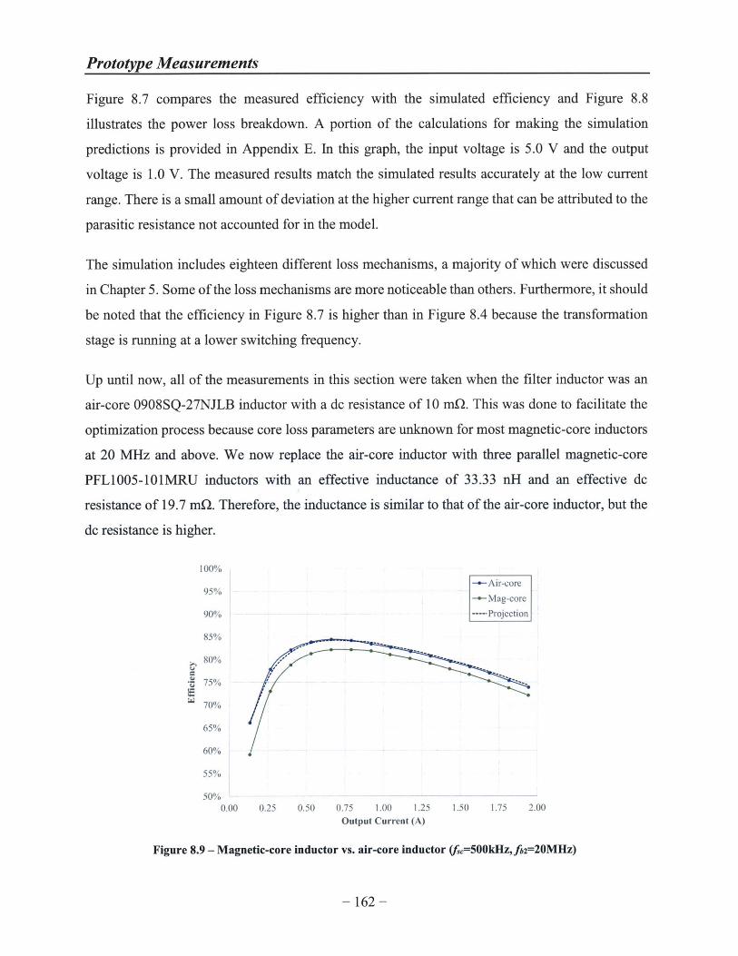
Prototype Measurements
Figure 8.7 compares the measured efficiency with the simulated efficiency and Figure 8.8
illustrates the power loss breakdown. A portion of the calculations for making the simulation
predictions is provided in Appendix E. In this graph, the input voltage is 5.0 V and the output
voltage is 1.0 V. The measured results match the simulated results accurately at the low current
range. There is a small amount of deviation at the higher current range that can be attributed to the
parasitic resistance not accounted for in the model.
The simulation includes eighteen different loss mechanisms, a majority of which were discussed
in Chapter 5. Some of the loss mechanisms are more noticeable than others. Furthermore, it should
be noted that the efficiency in Figure 8.7 is higher than in Figure 8.4 because the transformation
stage is running at a lower switching frequency.
Up until now, all of the measurements in this section were taken when the filter inductor was an
air-core 0908SQ-27NJLB inductor with a dc resistance of 10 mK. This was done to facilitate the
optimization process because core loss parameters are unknown for most magnetic-core inductors
at 20 MHz and above. We now replace the air-core inductor with three parallel magnetic-core
PFL1005-101MRU inductors with an effective inductance of 33.33 nH and an effective dc
resistance of 19.7 mQ. Therefore, the inductance is similar to that of the air-core inductor, but the
dc resistance is higher.
100%5 Air-core
95%-+Mag-core
90% Projection
85%
80%
75%
70%
65%
60%
55%
50%0.00 0.25 0.50 0.75 1.00 1.25 1.50 1.75 2.00
Output Current (A)
Figure 8.9 - Magnetic-core inductor vs. air-core inductor (fsc=500kHz,fb=20MHz)
-162-

Prototype Measurements
Figure 8.9 compares the measured efficiency of the prototype module using the air-core inductor
with that of the magnetic-core inductor. The dotted line is a projection that assumes the magnetic-
core inductor has the same dc resistance as the air-core inductor. In this figure, the input voltage
is 5.0 V and the output voltage is 1.0 V. As can be seen, the efficiency between the projection and
air-core inductor is quite similar when the output current is above 0.5 A. At light load, the deviation
in efficiency is as high as 7% at 0.1 A. This behavior is consistent with the addition of core loss.
Therefore, the impact on performance using magnetic-core inductors is minor.
The air-core inductor has a height of 1.829 mm with a 2.972 mm x 2.134 mm footprint, whereas
the magnetic-core inductors have a total height of 0.71 mm with a 1.14 mm x 0.635 mm total
footprint, thereby resulting in a 23-fold reduction in inductor volume. In addition, there is a slight
variation in performance between the module in Figure 8.9 and the module in Figure 8.7 due to
few missing bumps connected to the regulation stage (i.e., increased interconnect loss).
8.3 Prototype Comparison
There are numerous power converter modules in the marketplace today. Ease of use, reliability,
and simplicity (from a PCB footprint perspective) drives their appeal. As a result, there is typically
an added cost for these benefits. Table 8.1 shows a comparison of various commercial power
converter modules along with the prototype module from this thesis.
Part Input Frequency Peak Efficiency Max Output Volume Power Loss Power DensityVendor 3nu Frqec3ekEfcec a upu ouePwrLs oe estNumber Voltage (V) (MHz) @ Vo=1.2V Power (W) (mm) (kW/W) (kW/inch)
FB6832J Fuji Electric 2.7 - 5.5 2.5 86.5% @ Vin=3.6V 0.36W @ Vo=1.2V 5.76 0.006407 1.024
EP5362Q Enpirion 2.4 -5.5 5.0 79.0% @ Vin=5.OV 1.20W @ Vo=1.2V 23.10 0.003762 0.851
EN6337QI Enpirion 2.375 - 6.6 2.0 85.0% @ Vin=5.oV 3.60W @ Vo=1.2V 138.75 0.005667 0.425
MIC3385 Micrel Semi 2.7 -5.5 8.0 78.0% @ Vin=5.OV 0.72W @ Vo=1.2V 9.45 0.003545 1.249
LTM4601 Linear Tech 4.5-28 0.9 88.5% @ Vin=5.OV 14.4W @ Vo=1.2V 630.00 0.007696 0.375
LTM4604 Linear Tech 2.35 - 5.5 1.25 85.0% @ Vin=5.oV 4.80W @ Vo=1.2V 310.50 0.005667 0.253
This Work MIT 2.7 -5.5 20.0 85.0% @ Vin=5.oV 2.40W @ Vo=1.2V 17.80 0.005667 2.210
Table 8.1 - Comparison of various commercial power converter modules
As can be seen from the table, the prototype module has a maximum output power of 2.4 W and
consumes a volume of 17.80 mm3. Consequently, the power density is 2210 W/inch 3 with an
- 163 -

Prototype Measurements
efficiency greater than mid-eighties at 1.2 V. In comparison, the EN6337QI, which has similar
specifications with regard to input voltage range, maximum output current, and efficiency has a
power density of 425 W/inch3. This corresponds to a 5.2-fold improvement in power density.
Figure 8.10 plots the power density versus switching frequency of the power converter modules
from Table 8.1. As can be seen, the power density increases as the switching frequency increases.
This behavior, which is alluded to in eqn. (1.7), is the reason there is a continued trend to push up
the switching frequency in both industry and academia. The challenge is then to decrease the
converter volume without sacrificing efficiency.
2.5
2.0
1.5
1.0
0.5
0.00.0 5.0 10.0 15.0 20.0 25.0
Switching Frequency (MHz)
Figure 8.10 - Power density vs. switching frequency for various power converter modules (MIT top right)
To compare the various modules, both their power loss and volume must be normalized with
respect to their maximum output power. Therefore, for each module, Figure 8.11 plots the
maximum output power divided by the power loss on the y-axis and the power density on the x-
axis. It is desirable to be in the top right corner.
In the comparison, the output voltage is 1.2 V and the power loss is at the peak efficiency. As can
be seen, the prototype module has a superior efficiency-power density figure of merit when
compared to commercial power converter modules with similar input and output characteristics.
The prototype module is one point on the projected frontier, which is indicated using a dashed line.
-164-

Prototype Measurements
0.018
0.016
0.014
0.012
0.010
0.008
0.006
0.004
0.002
ProjectedFrontier
S
0* 0
0
ThisWork
0.0000.0 0.5 1.0
Pomax
1.5 2.0/ Vol (kW/inch 3)
Figure 8.11 - Normalized power loss vs. power density with frontier overlay
It is more than likely that all of the power converters in the commercial modules are Buck
converters. In light of this, Table 8.2 includes a comparative listing of some previous academic
work in this space with different power converter topologies.
Reference [90] [361 [781 [851 This Work
Publication Year 1997 2011 2012 2012 2013
Converter Topology Cascoded Buck Buck Cascoded Buck Merged two-stage Two-stage
CMOS node 0.15 pm 0.35 pm 0.35 pm 0.18 pm 0.18 pm
Input Voltage 3.3V 2.7 - 4.2 V 2.5 - 5.0 V 4.0 - 5.5 V 2.7 - 5.5 V
Output Voltage 1.65 V 2.4 V 1.0 - 1.8 V 0.8-1.3 0.6 - 1.2 V
Switching Frequency 12.8 MHz 5 MHz 1.3 MHz 10 MHz 20 MHz
Peak Efficiency (flpk) 75% 91% 94% 81% 85%
Voltage step-down atlpk 3.3 - 1.65 V 3.3 - 2.4 V 2.5 - 1.8 V 5.0 - 1.3 V 5.0 - 1.2 V
Output power range 8.25 - 82.5 mW 0.12 - 1.2 W 18 - 675 mW 0.3 - 0.8 W 0.2 - 2.4 W
Table 8.2 - Comparison of various academic works
- 165 -
2.5 3.0

Prototype Measurements
The prototype module achieves the largest voltage step-down ratio, while operating at a higher
switching frequency than many of the other converters and with comparable efficiencies. The split-
power architecture demonstrates superior performance compared to previous academic work
largely due to improvements in architecture, circuit design, and packaging.
-166-

Chapter 9 - Summary and Conclusions
This thesis presented a two-stage power conversion architecture, design techniques, and packaging
requirements necessary to create power converters with an efficiency-power density figure of merit
that is superior to conventional power converters. Furthermore, the resulting power converters can
provide numerous low-voltage outputs over a wide input voltage range with a very fast dynamic
response and are therefore ideal for powering logic devices in the mobile and/or high-performance
computing markets.
9.1 Summary
The first half of the thesis set the stage for the introduction of a two-stage power converter
architecture, introduced in Chapter 5. In the first chapter, we addressed the motivations for the
thesis work and the current state of the art in power converters. Next, we presented a background
on various IC technology and its importance with respect to power converters. In Chapter 3, we
provided a review of switch-mode power converters, switched capacitor power converters, and
other two-stage power converters. In the fourth chapter, we compared the energy storage
components used in these power converters. As it so happens, in the application space of interest,
the available capacitors can store at least two to three orders of magnitude more energy per volume
than inductors.
Chapter 5 introduced the split-power architecture, which is a two-stage power conversion
architecture where the transformation and regulation functions of a power converter are separated
into two specialized stages. Superior performance is achieved by combining the strengths of
switched capacitor (SC) techniques (small size, light-load performance) with the high efficiency
and regulation capability of switch-mode power converters, thereby exploiting the asymmetry in
power density between capacitors and inductors.
To demonstrate the superior efficiency-power density of the split-power architecture, we created
a prototype power converter that was designed in Chapter 6, packaged in Chapter 7, and tested in
Chapter 8. The demonstration vehicle was a 2.4 W dc-dc power converter implemented in a 180 nm
CMOS IC process and co-packaged with its passive components producing a module. It operates
- 167 -

Summary and Conclusions
from an input voltage of 2.7 V to 5.5 V, provides an output voltage of < 1.2 V, and achieves a 2210
W/inch3 power density with an efficiency greater than 80%. This prototype module outperforms
competing offerings from both academy and industry. It is also is just one instance of the split-
power architecture with a focus on volume rather than efficiency.
9.2 Future Work
Even though our prototype module has superior performance when compared to both commercial
and academic works, there are three major areas of improvement. First, the efficiency of the
transformation stage can be improved by changing the type of SC converter in the transformation
stage. As shown in Section 5.4, a cascade multiplier topology is a better choice for this architecture.
Second, the packaging efficiency of the module could be increased: as it stands, the packaging
efficiency of the prototype module is approximately 30%. The power density would be boosted
from 2.21 kW/inch 3 to 4.42 kW/inch 3 if the packaging efficiency were increased from 30% to
60%. Third, a custom-made high frequency inductor could be developed to complement the
prototype module. This would allow us to push the switching frequency above 20 MHz without
sacrificing efficiency.
- 168 -

Appendix A - FOM with S/ID Charge
In this appendix, we discuss how the charge in the source and drain influences a MOSFET's figure
of merit. The source and drain regions in a MOSFET each consist of a p-n junction. In typical
operation, the source is connected to the bulk. Consequently, the source p-n junction does not
consume charge. Figure A. 1 illustrates a diagram of an abrupt p-n junction.
- VA +
neutral depletion neutral
p-region + n-region
+ holeselectrons: + hoe
* S XE-field
0 Charge + +
- x
Figure A.1 - Abruptp-n junction diagram
In a p-n junction, holes from the p-region diffuse into the n-region where the hole concentration is
low. Similarly, electrons from the n-region diffuse into the p-region where the electron
concentration is low. The migrated holes consequently leave behind negatively charged acceptors
in the p-region and the migrated electrons leave behind positively charged donors in the n-region.
As a result, a space charge region is formed, which creates a built-in electric field. This region is
also known as a depletion region [83].
The amount of charge in the depletion region is a function of its width Wd and the concentration of
exposed donors and acceptors. The exact amount of stored charge in terms of the applied voltage
VA is given by
-169-
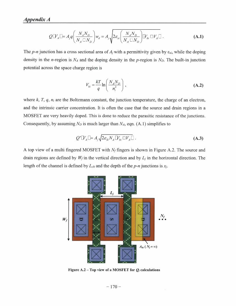
Appendix A
N NNNQ ,- Aq A D wd= A 2cs, NAND > bYi DVAD. (A.1)
The p-n junction has a cross sectional area of A; with a permittivity given by ssi, while the doping
density in the n-region is NA and the doping density in the p-region is ND. The built-in junction
potential across the space charge region is
v kTl(NND~
Vb = In 2 (A.2)q ni
where k, T, q, ni are the Boltzmann constant, the junction temperature, the charge of an electron,
and the intrinsic carrier concentration. It is often the case that the source and drain regions in a
MOSFET are very heavily doped. This is done to reduce the parasitic resistance of the junctions.
Consequently, by assuming ND is much larger than NA, eqn. (A. 1) simplifies to
Q'E=A A 2 eSINA EVY, DVAD. (A.3)
A top view of a multi fingered MOSFET with Nf fingers is shown in Figure A.2. The source and
drain regions are defined by Wf in the vertical direction and by L; in the horizontal direction. The
length of the channel is defined by Lch and the depth of the p-n junctions is x;.
WI eNf
Figure A.2 - Top view of a MOSFET for Q calculations
-170-

Appendix A
The total amount of charge in the source junction or drain junction in a MOSFET is the
combination of the charge Qbot from the bottom of the junction and the charge Qside along the
sidewall of the junction, resulting in
Qj = ()b, L Qsid ' (A.4)
Both of these charge contributions can be calculated using eqn. (A.3). If Nf is large then
Qbt = )-.5N 1WL E, NA(Vi VD D) (A.5)
and
(A.6)Qside = xNf 174 D2L 2 eSiNA(V, U VDD
By plugging eqns. (A.5) and (A.6) into eqn. (A.4), we obtain
Q1 =[7A).5NJWJLJBIX-NJ xW 1 LIL], L2 N(Vi L VDD) (A.7)
In Section 2.1.1, we verified that Lj=3 xLeh. If we use that result and assume Wf>> 2Lj, then eqn.
(A.7) can be simplified into
Q1 =Wj2 Es E bVDD)N, [J.5 L i -, E, (A.8)
where
W=N xWf f* (A.9)
For completeness, we rewrite eqn. (2.7) in two different ways. First, we rewrite eqn. (2.7) so that
the charge in the channel is given by
Qch =Cx 7DD Lh ,= LhW7IDD Vh1tox
(A.10)
Second, we rewrite eqn. (2.7) so that the resistance of the channel is given by
h h -h
PinvQch /inv'oxW[YDD L VhF]
(A.11)
- 171 -

Appendix A
The figure of merit in eqn. (2.8) only includes the charge in the gate. It does not include the charge
in the source or drain regions. This can be remedied by defining a new figure of merit as
FOM2 = RCh chQJ I . (A.12)
The charge Qj of only one junction is included because, in typical operation, the source is
connected to the bulk. By plugging eqns. (A.8) through (A. 11) into eqn. (A. 12), we obtain
FOM 2 = LChtox - -C[ Lch F'1"DD Jh§W 2 Ss (Vb, DVDD)NA [.5. (A.13)/-inv ox E"'DD V _ ox
By assuming VDD >> Vth and VDD >> Vbi, then eqn. (A. 13) can be reduced to
FOM2 Lch tOx [Ox L 2iENA J.5Lh wxi . (A.14)
PinvEo _tox VDD
In constant-field scaling, tox, Le, W, x;, and VDD are scaled by 1/K while the doping concentrations
(NA, ND) are scaled by K [33]. Figure 2.3 shows a diagram of a constant field scaled device along
with the original device.
If the devices are scaled down using constant field scaling, then we obtain
FOM2 1 2 (A.15)K
It is important to note that we can also restate eqn. (A. 15) as
FOM 2 c KD. (A.16)
Furthermore, if we assume
Ron= Rh L 2Rt Rh (A.17)
C, =C.h D 2 Cf CCh (A.18)
and
Qch LQj =ch DCJ jDD, (A.19)
- 172 -

Appendix A
then we obtain
R00 9 rLIjOCD (A.20)R ' C 5C VDD *
The Ron(Cg+Cj) product for various CMOS processes is plotted versus supply voltage in FigureA.3.The devices used were minimum feature size core NFETs. To help aid in comparison, we havealso plotted the RonCg product in Figure A.4 using the same NFETs.
3.5E-03 3.OE-03 - - -- - - --- - - - ---
3.OE-03 2.5E-03
R'= 0.92772.5E-03
R2
=0.8987.2.OE-03
E2.0E-03
+..E-03
.EOE-03S.OE-03
5.OE-04 * 5.OE-04
0.OE+00 0.OE+000.0 0.5 1.0 1.5 2.0 2.5 3.0 3.5 4.0 0.0 0.5 1.0 1.5 2.0 2.5 3.0 3.5 4.0
Supply Voltage (V) Supply Voltage (V)
Figure A.3 - Ron(Cg+Cj) vs. supply voltage for core Figure A.4 - RonCg vs. supply voltage for coreNFETs NFETs
It can be seen from the figure above that indeed the Ron(Cg+C) product is proportional to the supplyvoltage as eqn. (A.20) predicts. There is some deviation from the linear fit in both figures, but theR2 of the trend line for the Ron( Cg+C;) data is quite good. It is even slightly higher than the R2 ofthe trend line for the RonCg data. This signifies that the inclusion of the junction charge leads to abetter fit between the theory and process data.
- 173 -

Appendix B - Barium Titanate
The discovery of barium titanate in the 1940s was the very beginning of the present-day era of
multi-layer ceramic capacitors, or MLCCs. At the time of discovery, it had a dielectric constant
that was at least two orders of magnitude greater than any previously known ceramic. It might be
surprising to know that in 1946 four distinguished engineers published the statement, "Barium
titanate, on the other hand, cannot be recommended as a capacitor dielectric except in special
cases" [110]. To their credit, barium titanate at the time had many undesirable features when
compared with the well-established dielectrics of impregnated paper, mica, steatite, and rutile. Its
permittivity varied with temperature and voltage. It also had a much shorter shelf life.
Barium titanate is a ferroelectric material and, by definition, it possesses a spontaneous (i.e.,
permanent) electric polarization, which can be reversed by application of an external electric field.
Nowadays, ferroelectric materials have become so dominant that capacitor standards incorporate
many ferroelectric-related idiosyncrasies. These materials have many uses such as MLCCs,
piezoelectric transducers, ferroelectric memories, and so forth.
The first description of barium titanate was published in the United States in 1942. During that
time, the United States led research on alternative dielectrics due to the scarcity of high-grade mica
and its importance to the war effort (World War II). As part of this program, a wide range of
titanate compositions were first created at Tamco Laboratory under the leadership of Eugene
Wainer [111]. His work established the basis for barium titanate research in the United States and
around the world [50]. A case can be made that there might have been an earlier synthesis of
barium titanate, but without recognition of its dielectric nature [18]. In this section, we describe
the single crystal and polycrystalline behavior of barium titanate and the properties associated with
these two forms.
B. 1 Single Crystal Behavior
Barium titanate is a ceramic material with the chemical formula BaTiO3. It can crystallize into two
distinct polymorphic forms: perovskite structure and hexagonal phase. Both forms are
ferroelectric, but we focus on the perovskite structure because this is what is used in ceramic
-174-

Appendix B
capacitors. A perovskite structure is any material with the same crystal structure as calcium
titanium oxide (CaTiO 3). The unit cell of BaTiO3 with a cubic lattice is shown in Figure B. 1. It is
composed of five atoms with the barium and oxygen ions together forming a face-centered cubic
lattice. The titanium ion occupies the octahedral interstitial site in the center.
O Barium
0 Titanium
O Oxygen
Figure B.1 - Cubic perovskite unit cell of barium titanate
There are four stable crystal phases of BaTiO3 with a perovskite structure: cubic, rhombohedral,
orthorhombic, and tetragonal - see Figure B.2. At high temperatures, BaTiO3 is paraelectric and
has a cubic phase. As the temperature is lowered, BaTiO3 undergoes three ferroelectric phase
transitions; the sequence is cubic -+ tetragonal -+ orthorhombic -> rhombohedral. Each phase
transition is accompanied by small atomic displacements resulting in a spontaneous polarization
aligned along the [001], [110], and [111] directions in the three ferroelectric phases, respectively.
278K - 393K
a2
a1
183K - 278K
a 3
C
a,
0 - 183K
a
a3 aa a2
a1
Tetragonal Orthorhombic
Figure B.2 - Barium titanate's crystal phases
Rhombohedral
- 175 -
398K - oo
a 3a 2
a,
C
Cubic
..... -- - -

Appendix B
The "eight site" order-disorder model can explain why there is spontaneous polarization in three
of the four phases [28]. In this model, there is a total of eight locations for the Ti4l ion to reside.
All eight "sites" are equally probable (i.e., disordered) when BaTiO3 is in its cubic phase as
depicted in Figure B.3a. However, when BaTiO3 is in the tetragonal phase, the top four "sites" are
preferred due to asymmetry, resulting in a net dipole moment as shown in Figure B.3b. By
continuing with this logic, two sites are preferred in the orthorhombic phase and one site is
preferred in the rhombohedral phase. As the temperature is lowered, the system becomes more
ordered. The assumption that only the Ti4l is displaced is a simplification. In reality, the oxygen
ions can move as well, resulting in long-range coupling effects (i.e., soft modes [25]).
c a2 ca2a1 a,
(a) Cubic phase (no polarization) (b) Tetragonal phase (up polarization)
Figure B.3 - Eight site model for perovskite ferroelectrics in tetragonal phase
The theoretical bias for the "eight site" order-disorder model is due to softening of short-range
repulsions by covalent hybridization. The displacement of the Ti41 ion is allowed because the Ti4l
3d electrons strongly hybridize with oxygen's 2p electrons [27]. This weakens the coulomb
repulsion between the Ti41 ions and 0 ions.
Barium titanate exhibits a distinct form of ionic polarization where the induced dipole is
spontaneous. As we previously explained, the top four "sites" are preferred when BaTiO 3 is in the
tetragonal phase. However, if an opposing electric field is applied, then it is possible to reverse the
direction of the spontaneous dipole moment. A transition from "polarization up" to "polarization
down" is represented by changing the preferred site locations for the Ti4l ion.
-176-

Appendix B
In general, the dielectric constant along the a-axis and c-axis of BaTiO3 varies greatly with
temperature [70]. There are three relative maxima, each occurring at the three phase transitions.
The maximum at 398 K is called the Curie point Tc. This is the temperature at which BaTiO3
transitions between the paraelectric phase and the ferroelectric phase. BaTiO3 is highly anisotropic
due to the crystal asymmetry. For instance, at room temperature (25 C), the dielectric constant
along the tetragonal c-axis is 400, whereas the dielectric constant along the a-axis and b-axis is
4000. Intuitively, this makes sense; it should be easier to move the Ti4l ion among the four
preferred sites rather than away from them.
B.2 Polycrystalline Behavior
Barium titanate is typically produced from powder into a bulk material that is polycrystalline. The
small crystals or crystallites of are often referred to as grains, which can vary in size and
orientation. Their direction can be random or directed, usually dependent upon growth and
processing conditions. The front view of a cubic grain of BaTiO3 is shown in Figure B.4a [6]. The
edges of the grain are rotated by 450 with respect to crystallographic a-axis and c-axis, while the
remaining edge of the grain is aligned with the b-axis. The dotted lines show the grain in the
paraelectric phase, while the solid line shows the grain in the tetragonal ferroelectric phase. The
edges of the sheared grain gi and gi are longer than go while the third edge (into the paper) is
shorter than go.
A Z
tT 3
Stressgo g1 P T1 P P P P P T1
b -0 ----- ---- --- TT3
(a) (b) (c)
Figure B.4 - Electric domain splitting
- 177 -

Appendix B
Unfortunately, in a polycrystalline material, the grain is clamped by its neighbors. Therefore,
during a paraelectric to ferroelectric phase transition, homogeneous stress builds up within the
grain. To minimize the stress energy, the grain will typically split into multiple electric domains.
This is referred to as domain twinning [22]. This concept is illustrated in Figure B.4b, where the
initial grain is split into five electric domains with polarizations 900 to each other. As a result,
stress energy is minimized by replacing the homogeneous stress in the grain with inhomogeneous
stresses around the upper and lower face of the grain as depicted in Figure B.4c.
The physical origin of domain twinning is the minimizing of energy fields, and the size of the
domain is a balance of energies. The larger the domains, the larger the electric and stress fields,
which result in a larger electrical energy density U and a larger mechanical field energy density
Un. Conversely, the smaller the domains, the higher the domain wall energy density UW. The
domain size is determined by the minimum in the sum of the energies as given by
Utt = U. E U, 1 U, = minimum. (B.1)
In tetragonal phase, the type of domain twinning depends upon the grain size. In a fine grain
ceramic, stress is relieved using simple lamellar twinning, which is shown in Figure B.5a.
Unfortunately, this pattern is only two dimensional due to the confined volume of the grain. In
contrast, a more complex three-dimensional domain twinning pattern is possible in a coarse grain
ceramic. Banded domain twinning occurs as a result, which is shown in Figure B.5b [7]. This type
of twinning is far more effective at relieving stress because of the added degree of freedom.
(a) Lamellar twinning (b) Banded domain twinning
Figure B.5 - Electric domain configurations
- 178 -

Appendix B
In barium titanate, the spontaneous polarization magnitude Po is approximately 26x 10-6
coulomb/cm 2 at room temperature [71]. However, the grain's polarization magnitude Pg is not
equal to Po. For example, in the case of lamellar twinning, the grain's polarization magnitude is
(B.2)Pg = P / 2 ,
whereas, in banded domain twinning it is
(B.3)
Therefore, Pg in a lamellar twinning pattern is quite a bit larger than in a banded domain twining
pattern, but so is the stress. Moreover, the grain's polarization vector in both twinning patterns can
point in one of twelve possible crystallographic [110] directions. Every grain must choose one of
the 12 directions during a paraelectric to ferroelectric phase transition [8].
E
CATHODE
ANODE
Figure B.6 - Polycrystalline structure
Figure B.6 illustrates a diagram of a barium titanate ceramic with a lamellar domain pattern. The
BaTiO3 grains are various sizes and randomly oriented. When there is an applied electric field E,
the spontaneous polarization field P of each grain will try to align with it. The switching process
is typically restricted to the remaining 11 crystallographic (110) directions. If all the grains are
switched to their fullest, the polarization of the ceramic is saturated. In this scenario, the
polarization of all the grains would point within a cone with an angle about 33.6' around the axis
-179-
, = P,2/ 3 [8].

Appendix B
of E (1/12 of a sphere). The resultant polarization is approximately 90% of the grain's polarization.
In many instances, the resultant polarization is smaller; it is typically in the 50% to 90% range [8].
During the polarization process, there are macroscopic changes in the dimensions of the grains and
the ceramic as a whole. Additionally, the original domain structure can be restored by reversing E
or by heating the ceramic above the Curie temperature.
The large dielectric constant of BaTiO3 ceramics is derived from two main sources. There is a
contribution from the intrinsic grain denoted by c,,vo, which is based upon the single-crystal
dielectric constant. There is also a contribution from the movement of domain walls within the
grain denoted by cr,dw. Therefore, the permittivity of a BaTiO3 ceramics can be calculated using
Er =vol L rIw (B.4)
The dielectric constant for a single domain grain can be calculated using Bruggeman's formula
[16] given by
r,,vol = ,, l 828 6KE, (B.5)4
The Ea and 8b values can either be obtained from measured data or calculated using Landau-
Devonshire-Ginzberg theory (LDGT). Devonshire built upon earlier ideas of Landau and Ginzberg
describes to the free energy of ferroelectrics as a function of polarization and stress [34].
It can be reasoned that the domain wall contribution Er,dw is proportional to the area Ad, of the 900
domain walls per volume, which is inversely proportional to the domain width Wd per volume,
therefore,
6r,dw O- (B.6)
Wd
The width Wd of the domain has shown to be a function of the grain size g in laminar twining. This
relation is expressed by
Wd C rg [9]. (B.7)
-180-

Appendix B
To bring everything together, eqn. (B.4) is simplified by inserting eqns. (B.5) through (B.7),
yielding
] aUE U SEEc K . (B.8)4
As can be seen, the permittivity of a BaTiO 3 ceramic is a function of both the quality of the grain
and its size. Typically, if the grain is small, the contribution from 8 r,vol is smaller than 6 r,vol. For
example, =r,vo= 1000 and 8 r,dw ~ 3000 when g = 1 [9]. The value of Ki depends upon the processing
conditions of the ceramic and can vary quite a bit.
In general, the permittivity of BaTiO3 starts to decrease when g is reduced below 1 Lm. This
behavior is more or less independent on processing conditions and is often referred to as the "size
effect". There are two major reasons for this behavior. To start off, there is a specific grain size
where the energy associated with the formation of domain-walls becomes too costly when
compared to the achievable reduction in energy due to twinning. Consequently, the grains become
single domain and the contribution from the domain wall movement disappears. Another major
reason is that the grains are actually a composite of a high Er tetragonal core and a low Cr cubic
surface layer. As the grain shrinks, the ratio between the core volume and surface layer volume
decreases, thereby lowering the effective permittivity of the grain [51]. The "size effect" is a large
obstacle to the development of future MLCCs and other nano devices.
- 181 -

Appendix C - Soft Ferrites
Soft ferrites are ceramic materials with ferric oxide (Fe203) as their principal component. They are
typically hard and brittle like most other ceramics. Magnetite is probably the oldest known ferrite
with the chemical formula Fe304. Naturally magnetized pieces of magnetite found in the earth's
crust are called lodestones.
It is surprising, then, that the first attempt to prepare ferrites was not made until the beginning of
the 2 0 th century. Even then, ferrites did not attract much attention because their magnetic properties
were less desirable than ferromagnetic alloys. However, in the 1950s, ferrites started to attract
attention when new applications arose that could take advantage of their unique properties. This
also happened to be when ferroelectric ceramics, such as barium titanate (BaTiO3), started to
become popular.
At the turn of the century, it was thought that ferrites were ferromagnetic. Louis N6el disproved
this theory with the discovery of two new forms of magnetic behavior: antiferromagnetism and
ferrimagnetism [79, 80]. Ferrites actually derive their magnetic properties from ferrimagnetism,
which was discussed in Section 4.1.2. In this section, we first describe the single crystal behavior
of soft ferrites. We then describe their polycrystalline behavior and then conclude with a short
section on core loss.
C. 1 Single Crystal Behavior
Magnetic ferrites fall into mainly two groups with different crystal structures: cubic and hexagonal.
We focus on the cubic group because it contains all of the commercially available soft ferrites,
which are often used to make transformer and inductor cores. In contrast, the hexagonal group
contains hard ferrites for use in permanent magnets.
Cubic ferrites have a spinel structure 8(Me" Fe2"..04), which is illustrated in Figure C. 1a. The large
spheres represent the oxygen ions, the small black spheres represent the ions in the A sites, and
the blue spheres represent ions in the B sites. The A sites and B sites can be occupied by divalent
metal Me" ions and/or trivalent iron Fe2"' ions. The large oxygen ions are in a face-center cubic
- 182 -

Appendix C
arrangement while the smaller metal (Me" and Fe2") ions occupy the space between them. The A
sites are tetrahedral while the B sites are octahedral. Therefore, the crystallographic environment
of the A and B sites are quite different.
o O\ OqoXO O DXOQ\ OoW 0o 0
XO X0O DXo oo oNooX~ oXo 0
(a) Unit cell (b) Magnetic moment alighnment (inverted)
Figure C.1 - Spinel crystalline structure
There are two different types of spinels ferrites: normal and inverted. In a normal spinel ferrite,
Me" ions occupy the A site, whereas, in an inverted spinel ferrite, Me" ions occupy the B site.
Some of the common Me" ions for each spinel type are shown in Table C. 1.
Spinel Type MeFe204 Me" Ferrimagnetic
Normal (Men )A(Fe"s)BO Zn, Cd NO
Inverted (Fe )A IeFeI)B 0 4 Mn, Fe, Ni, Cu, Mg YES
Table C.1 - Properties of spinel ferrites
Additionally, normal spinel ferrites are not ferrimagnetic, whereas inverted spinel ferrites are
ferrimagnetic. An explanation for this behavior is given later on in the section. In the inverted
spinel ferrite case, incomplete cancellation of the magnetic moments can be seen in Figure C. lb.
In general, a ferrite's magnetic properties are due to the magnetic ions it contains. The oxygen ions
within the ferrite do not have an effect because their net magnetic moment is zero. Hund's rule
- 183 -
4 I

Appendix C
states that the partly filled electron shells are arranged to produce the maximum spin unbalance.
For example, Fe2+ has six 3d electrons in the outer shell. Due to Hund's rule, five of the electrons
will be spin up, whereas the sixth electron will be spin down, thereby resulting in a spin-only
moment of 4 pB (5 pM - lyB). For reference, the magnetic moments of various transition metal ions
are given in Table C.2 [31].
Number Spin-OnlyIons of 3d Moment
electrons in pB
Sc 3+ Ti4* 0 0
TiV+ V4 _ 1 1
Ti2+ V 3+ Cre* 2 2V 2+ Cr 3+ Mn4+ 3 3
Cr 2+ Mn3* Fe 4+ 4 4Mn2+ Fe 3+ Co4 + 5 5
Fe2+ Co3 + Ni 4* 6 4
Co2+ Ni 3+ 7 3Ni 2+ 8 2
Cu2+ 9 1Cu+ Zn2+ 10 0
Table C.2 - Spin-only moments of ions of the first transition metal series
The net magnetic moment per molecule tH of a ferrite can be calculated if the following details
are known: the magnetic moment of each ion, the distribution of the ions between sites, and the
exchange interaction between the sites. The AB, AA, and BB site interactions all tend to be
negative, but the AB site interaction is usually the strongest. For example, in an Ni ferrite, all of
the Ni2+ ions occupy the B sites, while the Fe3+ ions are evenly divided between A and B sites.
Due to the negative AB site interaction, the Fe3+ ions in the A sites have moments that are
antiparallel to the Fe3+ ions in the B sites and the moments cancel out. Therefore, pH of a Ni ferrite
is simply the magnetic moment of the Ni2+ ion. In general, tH of any inverted spinel ferrite is the
magnetic moment of the divalent metal ion. This leads to the calculated values of pH shown in
Table C.3 [31].
Moreover, the normal spinel structure of Zn ferrite results in a different behavior. In this material,
the Zn2+ ion occupies the A site, but because its magnetic moment is zero there is no AB site
-184-

Appendix C
interaction. The negative BB site interaction now comes into play and the Fe3+ ions on the B sites
tend to have antiparallel magnetic moments, thereby canceling out. Consequently, pH of a Zn
ferrite is zero.
Ferrite Mn Fe Co Ni Cu Zn
Calculated pH 5 4 3 2 1 0
Measured pH 4.6 4.1 3.7 2.3 1.3 0
Table C.3 - Spin-only magnetic moments in common ferrites
Furthermore, it is possible to mix a normal spinel type ferrite with an inverse spinel type ferrite.
The resulting mixture is given by
Normal + Inverted = (Me,nrFeu )A (Meji" Fe r B, (C.1)
where y is the degree of inversion. When this is attempted, it is expected that a mixture (solid
solution) of a ferrite having practically no magnetization with a ferrite having strong magnetization
would result in a remarkable decrease in magnetization. Surprisingly, the opposite happens: the
addition of a non-magnetic ion actually increases the magnetization. This can be explained by an
example. Suppose we create a mixed ferrite containing 10 mol% Zn ferrite and 90 mol% Ni ferrite
as shown in row three of Table C.4 [31].
Tetrahedral Octahedral Net Moment# Material Structure
A Sites B Sites (pB/Molecule)
1 NiFe 20 4 Inverted Fe 3+ 5T Ni 2+ 24 Fe3' 54 24
2 ZnFe 2O4 Normal Zn2+ Of Fe3+ 54 Fe3+ 5T 04
0.9NiFe2O4 Inverted 0.9Fe 3+ 4.5T 0.9Ni2+ 1.84 0.9Fe3* 4.54
3 0.1ZnFe20 4 Normal 0.1Zn 2+ OT 0.1Fe3* 0.54 0.1Fe3+ 0.54
4.51T 2.341 5.041 2.84
Table C.4 - Ion distribution and net moment per molecule in NiZn ferrite
The Zn2+ ion from the Zn ferrite has a zero magnetic moment, thereby weakening the A site's
magnetic moment. Furthermore, the Fe3+ ions from the Zn ferrite have parallel magnetic moments
due to strong AB ion interactions, thereby strengthening the B site's magnetic moment.
- 185 -

Appendix C
Consequently, pH has increased from 2.0ptB for a pure Ni ferrite to 2 .8 tB for this mixed NiZn
ferrite. Increasing the Zn content will further increase pH with a maximum value of approximately
5pJB at a 50/50 mixture [38], at which time the A site's magnetic moments will become too weak
to affect the B site's magnetic moments. As a result, mixed ferrites are very popular - two of most
common compositions are MnZnFe204 and NiZnFe2O4.
Once pH is known for a particular ferrite, its saturation magnetization Ms can be calculated using
= n H(C.2)MS 3a
The unit cell's lattice constant a is required along with the number of magnetic dipoles nm per unit
cell. In the case of a spinel crystal, there are eight molecules per unit cell. Table C.5 shows Ms for
some common magnetic materials [31].
Substance PH fm a (nm) Ms (emu/cm3 )
CuFe20 4 1.3pB 8 0.837 164.4
NiFe 20 4 2.3pB 8 0.834 294.0
CoFe 20 4 3.7pB 8 0.838 466.3
Fe"Fe 20 4 4 .l pB 8 0.839 514.8
MnFe 20 4 4 .6 pB 8 0.850 555.5
Fe 2 .2 2 pB 2 0.287 1741.0
Table C.5 - Saturation magnetization of common ferrites
Typically, ferrites have a Ms in the 150 to 550 emu/cm 3 range and can be pushed a bit higher (-700
emu/cm 3) by creating a mixed ferrite. In contrast, iron has a much higher Ms, even though it has a
lower ptH. This is because the unit cell of iron is a body center cubic (BCC) structure with 2 atoms
per unit cell. Unfortunately, iron's other magnetic properties are not as appealing.
C.2 Polycrystalline Behavior
Soft ferrites are similar to ferroelectric ceramics, such as barium titanate, in numerous ways.
Among other similar traits, ferrites are polycrystalline, they have domains, they saturate, and so
forth. In many respects, soft ferrites can be thought of as a magnetic analog to ferroelectrics.
-186-
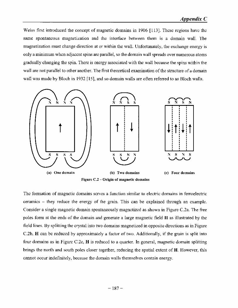
Appendix C
Weiss first introduced the concept of magnetic domains in 1906 [113]. These regions have the
same spontaneous magnetization and the interface between them is a domain wall. The
magnetization must change direction at or within the wall. Unfortunately, the exchange energy is
only a minimum when adjacent spins are parallel, so the domain wall spreads over numerous atoms
gradually changing the spin. There is energy associated with the wall because the spins within the
wall are not parallel to other another. The first theoretical examination of the structure of a domain
wall was made by Bloch in 1932 [15], and so domain walls are often referred to as Bloch walls.
N N N N
S S SS
(a) One domain
Figure
N N S S
S S N N
(b) Two domains
C.2 - Origin of magnetic domains
SNSNS S5 5 5S SS SS S
S SS SS Sa aS Sa aa aa aa a
NS NS
(c) Four domains
The formation of magnetic domains serves a function similar to electric domains in ferroelectric
ceramics - they reduce the energy of the grain. This can be explained through an example.
Consider a single magnetic domain spontaneously magnetized as shown in Figure C.2a. The free
poles form at the ends of the domain and generate a large magnetic field H as illustrated by the
field lines. By splitting the crystal into two domains magnetized in opposite directions as in Figure
C.2b, H can be reduced by approximately a factor of two. Additionally, if the grain is split into
four domains as in Figure C.2c, H is reduced to a quarter. In general, magnetic domain splitting
brings the north and south poles closer together, reducing the spatial extent of H. However, this
cannot occur indefinitely, because the domain walls themselves contain energy.
- 187-

Appendix C
As the size of the magnetic domain increases, the crystal's magnetostatic energy density Uns
increases. Conversely, as the size of the magnetic domain decreases, the domain wall energy
density Uwail increases. Eventually, an equilibrium domain size will be reached as the domains are
split. The size of the magnetic domain is determined by the minimum in the sum of the energies
as given by
U,,, =U,, DU,,l = minimum. (C.3)
The progression of magnetic domains as H grows is illustrated in Figure C.3 [57]. With increasing
H, favorable magnetic domains will grow in volume via domain-wall motion, thereby lowering
the magnetic potential of grain. Domain wall motion will continue until all but the favored
magnetic domains within a grain remain as shown in Figure C.3c.
y
Applied field (a) Unmagnetized (b) Domain growth
(c) Domain growth (max) (d) Domain rotation (e) Domain satuation
Figure C.3 - Fundamental magnetization processes
To further increase the magnetization, the magnetic moment of each domain can rotate towards
the direction of H as illustrated in Figure C.3d. This process is referred to as domain rotation and
is accomplished by the rotation of the net magnetic moment of each atom. The grain is said to be
saturated when the magnetic domains have grown as large as they can and the magnetization vector
is parallel with H as illustrated in Figure C.3e.
- 188 -

Appendix C
For a pure magnetic domain rotation, it can be shown that the static spin susceptibility is
m2
%spin,O - S (C.4)Hk
where the anisotropy field is given by the symbol Hk [39]. Crystal anisotropy can be thought of as
a magnetic field trying to hold the magnetization parallel to the axis. The magnitude of the crystal
anisotropy is a function of the energy required to overcome the spin-orbit coupling. Unfortunately,
it is generally not possible to calculate Hk from first principles for a given material. However, it is
known that lower crystal symmetry typically leads to larger crystal anisotropy.
The behavior of a magnetic material in response to an applied magnetic field is the combination
of domain wall motion and domain rotation. The relative permeability pr can be expressed as
p, =I E XsPin E Z - (C.5)
Typically, the spin contribution has a relaxation type behavior while domain wall contribution has
a resonance type behavior as given by
%spin,O
SPsin -I LI jo/coin (C.6)
and
2%dw,O r,dw
-dw 2 . (C.7)t, ) 2 0 j 8dC
r,,dw t)d
The static susceptibility of the domain wall motion is denoted by Xdw,o, the resonance frequency of
the domain wall motion is denoted by Or,dw, and the damping factor of the domain wall motion is
denoted by ,8d.
In high frequency ferrite materials, the dominate contribution to the permeability is often from the
domain rotation. The spin resonance frequency Orspin and %spin,o are actually linked by a physical
material constant. Jacob Snoek was the first observe this relation [99], which was theoretically
predicted by Landau and Lifshits in 1935 [61]. In a pure unstrained polycrystalline material, the
relation can be written
-189-
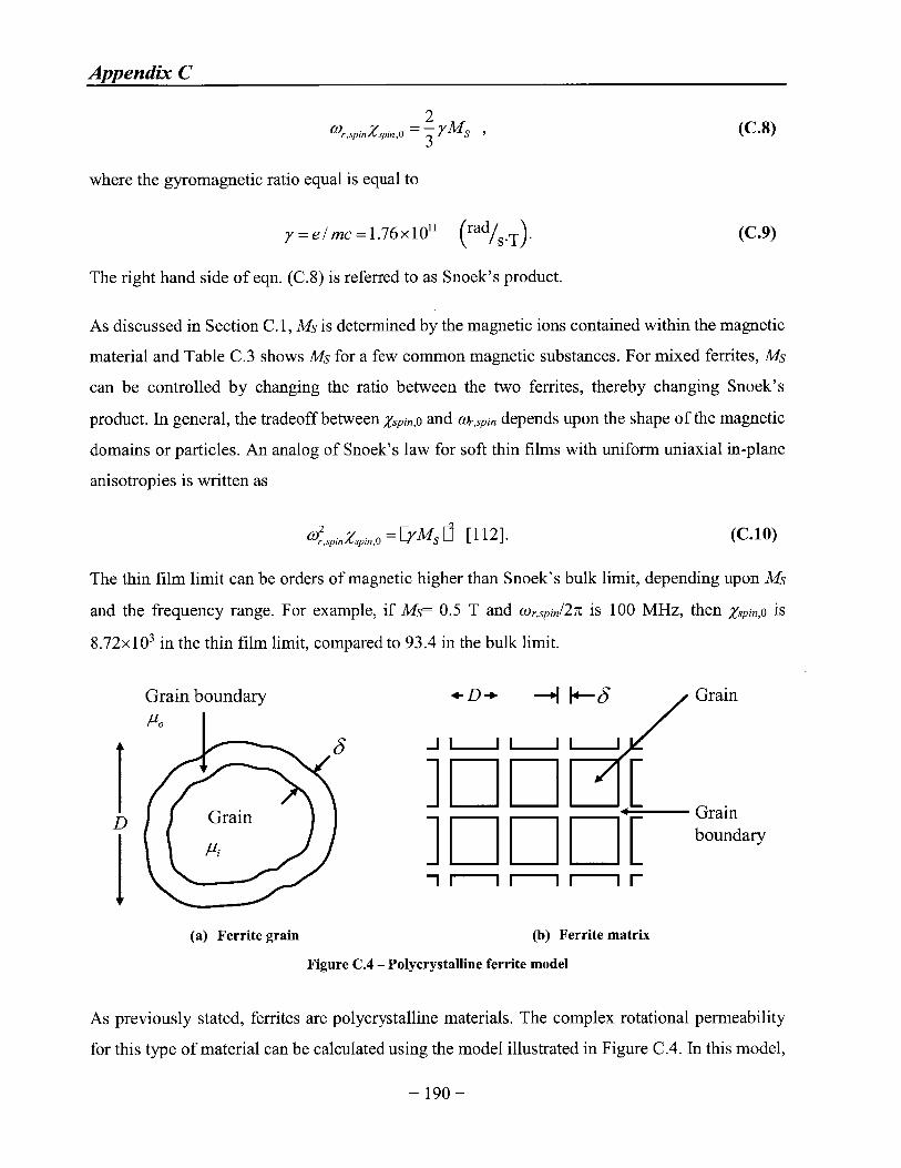
20,,,,pinXp,,O -2 YMS3
(C.8)
where the gyromagnetic ratio equal is equal to
y = e/ mc =1.76x10' (rad/s.T). (C.9)
The right hand side of eqn. (C.8) is referred to as Snoek's product.
As discussed in Section C. 1, Ms is determined by the magnetic ions contained within the magnetic
material and Table C.3 shows Ms for a few common magnetic substances. For mixed ferrites, Ms
can be controlled by changing the ratio between the two ferrites, thereby changing Snoek's
product. In general, the tradeoff between %spin,o and or,spjn depends upon the shape of the magnetic
domains or particles. An analog of Snoek's law for soft thin films with uniform uniaxial in-plane
anisotropies is written as
wo.sznpia'nO =[)Ms 1 [112]. (C.10)
The thin film limit can be orders of magnetic higher than Snoek's bulk limit, depending upon Ms
and the frequency range. For example, if Ms- 0.5 T and or,spin/27r is 100 MHz, then %spin,o is
8.72x 10³ in the thin film limit, compared to 93.4 in the bulk limit.
Grain boundary
Grain
(a) Ferrite grain
Figure
+-D+ -Grain
J LJ LJ LJ
Grain
] E Kboundaryi m m m r~~~I|
(b) Ferrite matrix
C.4 - Polycrystalline ferrite model
As previously stated, ferrites are polycrystalline materials. The complex rotational permeability
for this type of material can be calculated using the model illustrated in Figure C.4. In this model,
-190-
Appendix C
D

Appendix C
a polycrystalline ferrite is represented by a matrix of ferrite grains surrounded by a non-magnetic
grain boundary layer [55]. The ferrite grains have a diameter D with high intrinsic permeability pi
while the grain boundary layer has a thickness 6 with low permeability.
Assuming 6<< D, then the effective permeability is a function of grain size as given by
,Dpe = D (C.11)
For small grains, the effective permeability pe has approximately a linear dependence on grain
size, while for large grains the effective permeability pe approaches the intrinsic permeability pi
of a single crystal. This model is also consistent with Snoek's limit, assuming the ferrite grain is
consistent with the limit and has a relaxation type behavior. Therefore, the desired ratio of effective
permeability pe to effective resonance frequencyfie can be controlled by selecting the proper grain
size. This is a microscopic analog to controlling the permeability of an inductor's core by
introducing an air gap.
C.3 Core Loss
Power converters typically store energy in magnetic material only for a brief period; each
switching cycle, energy is pumped into and then out of the magnetic material. Unfortunately, the
magnetic material consumes energy as the magnetization field M inside the material changes.
The amount of energy loss per cycle is proportional to the area inscribed by the M versus H loop
and the B versus H loop. Typically, as the peak flux amplitude Bpk increases, the loop lengthens;
and as the frequencies fs, increases, the loop bulges - Figure C.5 illustrates this behavior.
Furthermore, the power loss consumed can be captured using the power law given by
tore = kf"Bo, (C.12)
where Pore is the time-average power loss per volume. The empirical coefficients are given by k,
a, and P. As it so happens, in 1892, Charles Steinmetz proposed a similar equation [100], where
he assumed a was equal to one. Consequently, eqn. (C. 12) is often referred to as the Steinmetz
equation.
- 191 -

Appendix C
/5
/
B
Bt
I + H /1/
Bt
-+/
/1(a) Flux sweep (b) Frequency sweep
Figure C.5 - Hysteresis loop in magnetic materials
The core loss versus ac flux density amplitude for a few high-frequency ferrite materials is shown
in Figure C.6 through Figure C.8, data from [47]. Furthermore, Table C.6 shows the empirical
coefficients obtained from curve fitting. It is surprising that the Steinmetz equation fits the core
loss in ferrite material quite nicely even though Steinmetz was trying to use a comparable equation
to model the core loss in iron alloys over a century ago.
1.OE+07 T
1.0E+06
1.0E+05 I
0.011.OE+04 1
0.001 AC Flux Density Amplitude (7) 0.01
Figure C.7 - Core loss for P material
-192-
1.0E+07 1
N40 Material" 20M~h
* 40MHz
" 60MHz
1.0E+06
1.OE+050.001
Figure
P Material
* 30MHz4 Mz
* 0wH
SiOWU
AC Flux Density Amplitude ()
C.6 - Core loss for N40 material
Z.-I,

Appendix C
I.OE+07
1.0E+06
0 1.OE+05
67 Material
*40MHz
-- t0MHz
-Steinmetz eq
1.0E+04 I0.001 AC Flux Density Amplitude (T)
Figure C.8 - Core loss for 67 material
Material k [W/m 3xHzaT4] a fl
P 7.80e-15 3.294 2.120
N40 1.30e-9 2.622 2.133
67 9.30e-9 2.512 2.057
Table C.6 - Steinmetz parameters for a few RFmaterials
0.01
Unfortunately, the Steinmetz equations only work well if the current is a purely sinusoidal.
Otherwise, the result will be incorrect. To remedy this issue, a few models have been developed
to address arbitrary waveforms [64, 108]. Most of these models use the basic Steinmetz
parameters.
- 193 -

Appendix D - Foil- Wound Inductor Design
In this appendix, a miniature high frequency foil-wound inductor is designed. The target
inductance was 33 nH at 30 MHz. The inductor utilizes magnetic material in order to reduce
inductor size. Unfortunately, at these high frequencies the available magnetic materials have low
permeabilities. It is well known that there is a fixed relationship between the maximum operating
frequency and permeability of a given magnetic material. This phenomena was first discovered by
J.L. Snoek in 1948 [99] and is given by
3100 u,. []1- -= 3 Ms ,(D.1)
2
where the gyrostatic ratio y is equal to e/mc=1.76x 106 and Ms is the saturation magnetization for
the ferromagnetic material. Due to this low permeability, both designs use un-gapped cores and
store all of the energy in the core itself resulting in low fringing fields. A diagram of each inductor
design is shown below.
Figure D.1 - Foil winding toroidal core
The inductor is of toroidal construction with a foil winding. The toroidal geometry has a high
degree of symmetry which leads to magnetic field cancellation outside the coil and hence less
electromagnetic interference (EMI). A rectangular core cross section was chosen since it is easy
to manufacture and provides a larger flux path than a circular core cross section. The foil winding
-194-

Appendix D
allows for very low dc resistance and low current crowding [101]. The actual design was a result
of an optimization done in MATLAB and shown in Table D. 1.
Part Number L (nH) Volume Height Rdc Pcore Shielded(mm 3) (mm) (mfl) (mW)
Foil-Wound 33.00 0.565 0.50 2.37 1.12 YES
0807SQ-22 22.00 6.620 1.40 10.00 0.00 NO
Table D.1 - Comparison of two RF inductors with a 500mA ripple
It can be seen from the table, the magnetic foil-wound inductor designs is superior in terms of
size and dc resistance when compared to solenoidal air-core inductors.
D.1 Optimization
The optimization procedure for a foil-wound inductor is now discussed. The geometry of the
inductor to be optimized is shown below. An isometric view is shown in Figure D.2 and a cross
sectional view is shown in Figure D.3.
:-d
d!Id.
Figure D.2 - Isometric view of the foil-woundinductor
Figure D.3 - Cross sectional view of the foil-woundinductor
The optimization procedure for the foil-wound inductor is a brute force method. The optimal
inductor design is found by sweeping various parameters, producing a large set of inductor designs
- 195 -
....{...

Appendix D
meeting the specified constraints. The inductor design with the lowest power loss is deemed the
optimal design. This approach might seem computationally intensive, but runs quite fast on current
generation desktop computers.
The optimization algorithm is shown in Figure D.4 and implemented in MATLAB. To start off
with, the physical constraints are entered, which are the inductor height h, the inductor diameter d,
and the core material selection. Next, the electrical specifications are entered, which are dc current
Id,, peak ac current Ipk, switching frequency fs, and desired inductance L. The code then runs
through three nested loops creating all of the possible inductor designs conforming to the physical
constraints while also meeting the electrical specifications. Once all of the designs are complete,
the code searches for the inductor design with the lowest power loss.
1: 1 all(I (I are colstants2: Id. I,. fs.. anw L are coistants3: for all in do1: for all d do
5: for all N do6: (alcu1late he. (1o. (d,. all(d By,
7: if e i< 0 the n8: conitille9: else if d/, < () then
10: coutinte11: else if d, < 2d, then12: conltille
1:1: else if B,,,,.,. > . then14: co tinIle
15: else16: calcIlate Pl,' ali(I Save17: end ift8: end for19: end for20: end for21: search for simallest P,.
Figure D.4 - Optimization algorithm of the foil-wound inductor
Each inductor design is created in the inner loop, which starts by first calculating the height of the
core using
-196-
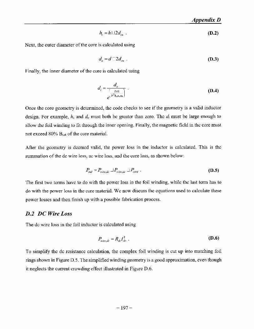
Appendix D
h = h E2de . (D.2)
Next, the outer diameter of the core is calculated using
d0 =d E 2d,, . (D.3)
Finally, the inner diameter of the core is calculated using
d2rL (D.A)
e N2h"p"po)
Once the core geometry is determined, the code checks to see if the geometry is a valid inductor
design. For example, h, and d, must both be greater than zero. The di must be large enough to
allow the foil winding to fit through the inner opening. Finally, the magnetic field in the core must
not exceed 80% Bsat of the core material.
After the geometry is deemed valid, the power loss in the inductor is calculated. This is the
summation of the dc wire loss, ac wire loss, and the core loss, as shown below:
mId = Pwire,dc wire,ac core . (D.5)
The first two terms have to do with the power loss in the foil winding, while the last term has to
do with the power loss in the core material. We now discuss the equations used to calculate these
power losses and then finish up with a possible fabrication process.
D.2 DC Wire Loss
The dc wire loss in the foil inductor is calculated using
Pwired = R 2 . (D.6)
To simplify the dc resistance calculation, the complex foil winding is cut up into matching foil
rings shown in Figure D.5. The simplified winding geometry is a good approximation, even though
it neglects the current crowding effect illustrated in Figure D.6.
- 197 -

Appendix D
Figure D.5 - Geometry used in wire loss Figure D.6 - Actual current density distribution fromcalculations Maxwell 3D
The dc resistance of the foil winding can be calculated by separating the foil rings into three
resistance elements as given by
Rd, =Rd, E ] Rind E Rtopbot,dc (D.7)
The dc resistance of the outer sidewall of the foil is
,dc N 2 p ,h - 4N2 puh (D.8)
Aou =4 [.dI2 El w E 2du l 4NdW,
The dc resistance of the inner sidewall of the foil is
,dc N 2 p u h - 4N 2pcuh (D.9)
Ao =EIA zEE 2d,, 1 d 2 4Ndcuw.
Finally, the dc resistance of the top and bottom of the foil is
RAopbotdc -= p In Td .l w (D.10)ed, rzd, EI Nwc)
By plugging eqns. (D.8) through (D. 10) into eqn. (D.7), we obtain
RdcN 2 pC h h L zd l Nwc (D.1)7rd, d, E du LI Nw do L du l Nw, 7rd 1 lNw
- 198 -

Appendix D
D.3 AC Wire Loss
The total ac wire loss in the inductor is the infinite summation of the power loss at each harmonic
frequency as given by
Pwire,ac = ,Rac, , (D.12)
where
= blpk I(D.13)
The Fourier coefficients bn are determined by the shape of the ac current waveform.
Similar to the dc wire loss case, the ac resistance of foil winding can be calculated by separating
the foil rings into three resistance elements as given by
Racn = RiRtac Li Rinac Ltopbotac (D.14)
However, unlike dc current, ac current has the tendency to flow mainly at the "skin" of the
conductor, reducing the effective cross section of the foil. The skin depth 6 is defined as the depth
at which the current density has fallen to l/e of the current density at the surface and is well
approximated as
PCU (D.15)
This effect can be taken into account by using 6 instead of the thickness of the foil when calculating
the ac resistance.
The ac resistance of the outer sidewall of the foil is
,cN 2 pe, IP D 28]E 4N 2 pe, Lk i28]ARutO, = = .Ebc 2 I (D.16)Ahe E Ars ta od2t i, E d5a E 4Ntfw
The ac resistance of the inner sidewall of the foil is
-199-

Appendix D
Rinac N 2 p. Eh, E 250 4N 2p, i, 2 15Aout EAn rc[L Ei29 3Jd 0 4Nw,-
(D.17)
Finally, the ac resistance of the top and bottom of the foil is
(D.18)Rtopbotac =N 2 P I 7rc do Nwb45 , rrd, ENw,
By plugging eqns. (D. 15) through (D. 18) into eqn. (D. 14), we obtain
R a,n N 2p hP. I2k h LI23 rE d LNW
'" d E o NW, d0 E t3 LNwI N d 1WNw (D.19)
D.4 Core Loss
The core loss can be calculated using the Steinmetz equation [100]. However, the B field in the
core is function of r, so the core loss can be calculated by integrating Steinmetz's equation (C.12)
from inner radius to the outer radius as
d0/2
" fore = J kf"B%2rh dr (D.20)d/2
The magnetic field in the inductor core is
B(r)= prp NIL2;r
(D.21)
thus
Bk(r) = B(r)|1L
1pk
PrPON'pk
2fzr(D.22)
The core loss can be solved by substituting the expression Bpk(r) from eqn. (D.22) into eqn. (D.20)
and then solving the integral, resulting in
Plore = kf"P Dulp1NI pk o he(2 Ef) 2 2 -
(D.23)
-200-

Appendix D
D.5 Manufacturing
We now discuss one possible fabrication process for this type of inductor, as shown in Figure D.7.
We first start with a base core material, most likely some form of ferrite or ferromagnetic alloy.
We then thin down the material, cut the outer diameter, and drill the inner hole. The order of
machining the inner and outer hole can be switched. A diamond drill or laser can be used to
machine the core material.
Once the core is fabricated, the winding needs to be formed. A foil-wound inductor has a very
complicated winding structure, which cannot be wound by hand. Instead, the winding is deposited
directly on the core. This winding process begins with the sputtering of a thin chromium adhesion
layer. Next, 1.0 ptm of copper is sputtered onto the core, followed by electroplating a thick copper
layer. In this case, the copper layer is 20 pim, but a thicker layer can be electroplated. The desired
thickness of the foil is typically part of the inductor design process.
4' S.
Base Material Thin Material Cutout Outer Drill InnerDiameter Diameter
Sputter Cr Sputter 1 sm Electroplate MachineAdhesion Layer Copper Layer 20pm of Copper Winding
Figure D.7 - Fabrication process of the foil-wound inductor
The last part of the fabrication process is machining the copper layer to form the winding. A simple
razor blade can be used to cut the copper [101] or micro-electrical-discharge machining (EDM)
can be used if high precision is required. EDM only removes conductive material so it is a perfect
fit for nonconductive cores, such as ferrites.
-201-

Appendix D
Figure D.8 - Different foil-wound inductor designs
Most electrical components, such as MLCCs and packaged ICs, are typically rectangular.
Therefore, if you try to arrange a foil-wound inductor with rectangular components on a PCB,
there is a lot of free space around the inductor. In general, a foil-wound inductor or any toroidal
inductor does not utilize the PCB area in the most efficient manner.
We propose two winding structures shown in Figure D.8, which utilize the PCB area more
efficiently. Both of these structures are only possible because the winding is deposited on the core
instead of being wound by hand. The easier of the two to fabricate is shown in the middle of Figure
D.8. It fills the hole inside of the toroid will metal and uses this area for the winding. This
effectively reduces the dc resistance of the winding without increasing its useable volume. The
second winding structure not only fills the hole inside of the toroid, but also fills the space around
the toroid using a similar concept as before. This winding structure or even the previous one is
most likely impractical. However, it is nice to imagine new ways of pushing the performance
boundary.
- 202 -
(N'K I I
Improving Performance

Appendix E - Buck Converter Code
% Purpose: evaluates the power losses in a Buck converter
% High-side device parameters: CgHO, CoHO, RHO, CwellO, WH
% Low-side device parameters: CgLO, CoLO, RLO, QrrO, WL
% NMOS parameters: CgnO, ConO, IsatnO% PMOS parameters: CgpO, CopO, IsatpO
% Filter Inductor parameters: Rdc, Rac, NbL, L
% Filter capacitor parameters: Rc, NbC
% Driver parameters: tap, b, N, wmin
% Interconnect parameters: deRate, RLowInt, RHighInt, Rb
% Operating point: vx, vout, vg, fs, iL, Iqui
% Created: 4/15/12, Last Modified: 4/15/13% Copyright 2012-2013, David Giuliano, MIT% May be freely used and modified but never sold. The original author% must be cited in all derivative work.
duty=vout/vx;ipkpk=(vout*(1-duty))/(L*fs);
tOFF=vg* (CgHO*tap* (1+b)+ConO+CopO*b)/(b*IsatpO);tON=vg* (CgHO*tap* (1+b)+ConO+CopO*b)/Isatn0;
duty=vout/vx;ipkpk=(vout*(1-duty))/(L*fs);
tOFF=vg* (CgHO*tap* (1+b)+ConO+CopO*b)/(b*Isatp0);tON=vg* (CgHO*tap* (1+b)+ConO+CopO*b)/Isatn0;
%% Calculate Switch Losses
PresL= (iL^2+ipkpk^2/12) *RLO/WL* (1-duty);
PresH= (iL^2+ipkpk^2/12) *RHO/WH* (duty);
PresLowInt=(iL^2+ipkpkA2/12)*RLowInt* (1-duty);
PresHighInt=(iLA2+ipkpkA2/12)*RHighInt*duty;
PresInt=(deRate-1)/deRate*(PresL+PresH)+PresLowInt+PresHighInt;
PresL=PresL*1/deRate;
PresH=PresH*1/deRate;
PgateL=vg^2*fs*WL*CgLO*1.0;PgateH=vgA2*fs*WH*CgHO*4/3;
-203 -

Appendix E
PoutL=0.5*vx^2*fs*WL*CoLO;PoutH=0.5*vx^2*fs*WH*CoHO;
PwellH=vx^2*fs*(WH*CwellO);
Psw=0.5*vx*iL*fs*(tON+tOFF);
%% Calculate Inductor Power Losses
PdcInd=iL^2*Rdc;
irms=ipkpk/(2*sqrt(2));PacInd=irms^2*Rac;
PcoreInd=O;
%% Calculate Capacitor Losses
PresCo=ipkpk^2/12*Rc;
%% Calculate Driver Power Losses
Wn=Wmin;
Wp=b*Wn;
Co=ConO*Wn+CopO*Wp;Cg=CgnO*Wn+Cgpo*Wp;
%% Calculate Upper Driver Loss
Cl=CgpO*WH;
h=(Co+Cg* (Cl/Cg)^(1/N))*vg*N;
d=(Cl/Cg-1)/((Cl/Cg)^(1/N)-1);
PdrvH=(vg*fs/N*d*h)-Cl*vg^2*fs;
%% Calculate Lower Driver Loss
Cl=CgnO*WL;
h=(Co+Cg*(Cl/Cg)^(1/N))*vg*N;d=(Cl/Cg-1)/((Cl/Cg)^(1/N)-1);
PdrvL=(vg*fs/N*d*h)-Cl*vg^2*fs;
%% Calculate Bump Losses
if NbL==O
PbumpInd=O;
else
PbumpInd= (iL^2+ipkpk^2/12) *2*Rb/NbL;end
if NbC==O
PbumpCap=O;
-204-

Appendix E
elsePbumpCap=(ipkpk^2/12)*2*Rb/NbC;
end
PresInt=PbumpInd+PbumpCap+Preslnt;
%% Calculate Misc Loss
Pqui=Iqui*vx;Pqrr=vx*fs*QrrO*WL;
%% Calculate Power LossPstage=PresL+PresH+PgateL+PgateH+PoutL+PoutH+PwellH+Psw;Ploss=Pstage+PdrvL+PdrvH+PacInd+PdcInd+PcoreInd+PresCo+PresInt+Pqui+Pqrr;
PowerLoss.resL=PresL;PowerLoss.resH=PresH;PowerLoss.gateL=PgateL;PowerLoss.gateH=PgateH;PowerLoss.outL=PoutL;PowerLoss.outH=PoutH;PowerLoss.wellH=PwellH;PowerLoss.sw=Psw;PowerLoss.drvL=PdrvL;PowerLoss.drvH=PdrvH;PowerLoss.acInd=PacInd;PowerLoss.dcInd=PdcInd;PowerLoss.coreInd=PcoreInd;PowerLoss.resCo=PresCo;PowerLoss.resInt=PresInt;PowerLoss.qui=Pqui;PowerLoss.qrr=Pqrr;PowerLoss.total=Ploss;
-205-

Appendix F- Interconnect Modeling
In this appendix, we discuss various interconnect models for use in IC design. A previously
proposed distributed gate resistance model is shown in Figure F. 1. It has been used to accurately
predict the cut-off frequency, maximum frequency of oscillation, thermal noise, and time response
of wide MOS devices in deep submicron technology [88].
R,/n R,/n RgIln
V1 V2 Vdn
(inV
-'out
Figure F.1 - Small-signal ac distributed gate resistance model
Based upon the figure above, we have created a distributed interconnect model with ideal current
sources as shown in Figure F.2. This model can be used to simulate the metal interconnect
resistance in a power MOSFET.
Rw y, R v2 Rw V3 Rw VnV0
Reff,1 n
Figure F.2 - Distributed interconnected model
The effective input resistance looking into the distributed interconnect model shown above is given
by
- 206 -

Appendix F
R- nl B' l (F.1)' 2 [h2I r R,
A general formula for the voltage drop across Rv is derived as
Av = v, Lv ], = (n D i)IR,. (F.2)
By plugging eqn. (F.2) into eqn. (F. 1), we obtain
nail
R =f 2 (F.3)i=O
where
R = RmTL (F.4)n
Substituting eqn. (F.4) into eqn. (F.3) and then expanding results in
Reffl = [ n2 E(n Ei)2 E(nE2)2
... Li] . (F.5)
Once eqn. (F.5) is simplified, we obtain
R,,L [n ?W iLD02n W 1]Rff,1 n3 6(F.6)
As n approaches infinity, we obtain
lim R effl(n)= RML (F.7)x-0 3
This result is quite useful. It illustrates that a metal line carrying a current that is equally distributed
among a series of current sources has an effective resistance that is 1/3 of its metal resistance.
The distributed interconnect model is a good representation of a multi-finger MOSFET as shown
Figure F.3. In this case, the number of fingers in the MOSFET is equal to n and each current source
-1 has been replaced with a small MOSFET. Additionally, a resistive via element R, has been added
to the drain of the each MOSFET in the model.
- 207 -

R v1 RW v2 RW RWV +
RV RV RV Rv
n
v,, RV
Figure F.3 - Multi-finger MOSFET model with interconnect resistance
It is important to note that the following analysis is only accurate when the MOSFET is operating
in saturation.
In order to find an exact solution for the effective input resistance Reff,2 in the multi-finger
MOSFET model, the node voltages vi - v, need to be solved. An example matrix is
2/R, 01/R 0
E1/R. 2/R. LA/R,0 w1/R, 2/Rw
0 0 0
0 0 0
0 W1/RW
0 0
0 0
... 2/R, W1/R,
0 1
The matrix above does not include Rv because their effect on the Reff,2 can be taken into account
after the node voltages are found. Once vi - v, are known, Re&2 can be calculated using
Reff, 2 - 1[I 1 [ i=O R. 1*
Furthermore, an approximate solution for Reff2 is given by
Reff,3 = 0 .
(F.9)
(F.10)
-208-
Appendix F
V1
V2
V3
V,
V
WIL11
Lil: i
EI1
(F.8)
vs

Appendix F
The term on the left side represents the contribution from the vias while the term on the right side
represents the contribution from the wires. Since current is fed from both sides, the term on the
right side, which originates from eqn. (F.7), is divided by four.
In addition, Reff3 can be written as a function of n by plugging eqn. (F.4) into eqn. (F. 10), yielding
Rff 3=&- D -n (F.11)n 12
Eqn. (F.9) and eqn. (F. 11) can now be compared, with the percent error between them being
error = x10eff,3 eff l . (F.12)Reff 2
To help visualize, eqn. (F. 12) is plotted versus n in the figure below.
0
-0.02
c.--0.04
0.
100 200 300 400 500MOSFET fingers (nf)
Figure F.4 - Percent error between Reff 2and Reft3 vs. number of MOSFET fingers
Another useful interconnect structure is shown in Figure F.5. This infinite ladder network can be
used to approximate a power device operating in triode mode, in contrast to the previous model,
which works when the power device is in saturation. For example, Rw can represent a portion of
the interconnect metal while R0 n represents a portion of the MOSFET's channel.
- 209 -
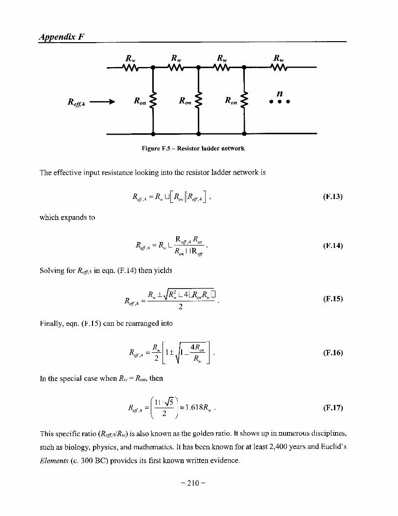
Appendix F
RW Rw Rw RW
nReff 4 Ron Ron Ron
Figure F.5 - Resistor ladder network
The effective input resistance looking into the resistor ladder network is
Rff 4 = R On R Rff,4 ], (F.13)
which expands to
R RR 4=R eff 4 "n
e~ff4 0RnL1 Reff(F.14)
Solving for Reff;4 in eqn. (F. 14) then yields
Re_ R, R D4OR, ERf,4 2
(F.15)
Finally, eqn. (F. 15) can be rearranged into
Reff4 = WL± ILI 4 "]2 1RW
(F.16)
In the special case when R, = Ron, then
Rff 4 =1 2 j[ 1.618Rw (F.17)
This specific ratio (Reff4/Rw) is also known as the golden ratio. It shows up in numerous disciplines,
such as biology, physics, and mathematics. It has been known for at least 2,400 years and Euclid's
Elements (c. 300 BC) provides its first known written evidence.
-210-

Appendix G - PCB Designs
G.1 Daughter Board
TO
IBUCKISC
VREF
VBG
VERR2
VSEL
VIN
Vss
Co C,
VSS Vss
IBUCK VDUTY
IsC IBIAS
VREF ESEL
VBG VDDUO
VERR2 EN BK
VSEL EN SC
VIN VO
Vss Vss
C2 C3
Vss vsS
T1
VDUTY
IBIAS
ESEL
VDD
EN BK
EN SC
Vo
Vss
Figure G.1 - Daughter board schematic
Parts Vendor Part Number DescriptionUo MIT MITDG001B prototype ICTo - Ti JAE Electronics AA03-PO20VA2-R6000 0.4 mm plugCo - C1 Taiyo Yuden TMK212B7105KG-T 1 pF, 0805, 25 V, X7R CAPC2 - C3 - not populated
Table G.1 - Bill of materials for the daughter board
Figure G.2 - Layout of the daughter board (layer 1 - top)
- 211 -

Appendix G
Figure G.3 - Layout of the daughter board (layer 2 - inner)
Figure G.4 - Layout of the daughter board (layer 3 - inner)
Figure G.5 - Layout of the daughter board (layer 4 - bottom)
-212-

Appendix G
G.2 Measurement Board
M 5.Ov
2.5v
R2 Ro R3 R4
T { R5 R1 R6 R,T3
-- isc 111AST'VWEF v
VBG VDD
T, VERR2 EN BK -
VIN EN SC
Cu C13VSEL ESEL--
d C11 1Vss Vss,
Rso s, S2 Fs31\
I An -. t1.8v
5enUdC9
U2 Ril U3 R2 U 1g~ C4 Rrd C6 R13
gnd R, C5 R9 C7 Ri
NC NC NC NC
S4 55 S6 S7
4 R42 R4 R4 R4 R5 R5 R5sR41 R4 R4f R4 R4 R 5 R5
- C14
Figure G.6 - Measurement board schematic
Parts Vendor Part Number Description
U1- U4 ADI ADR291FRZ-ND 1.8 V linear regulatorUs ADI ADP150AUJZ-1.8-R7CT-ND 2.5 V linear regulatorR40 - R54 Rohm Semi ESR10EZPF3R91 7.5 0, 1/4 W RESSo -S7 C&K GT11MCBE 3 terminal SPDTTo - T2 Keystone 7006 red binding postT3 - Ts Keystone 7007 black binding postT6 - T7 JAE Electronics AA03-SO20VA1-R6000 0.4 mm receptacleCo - CIO Taiyo Yuden TMK212B7105KG-T 1 pF, 0805, 25 V, X7R CAPC11 - C14 Taiyo Yuden LMK212BJ106KG-T 10 pF, 0805, 10 V, X5R CAPRo - Ri Panasonic ERJ-6ENF1002V 10 kf), 0805 RESR2 - R4 Copal ST32ETB103 10 kQ trim potRs- R7 Panasonic ERJ-6ENF2491V 2.49 k(, 0805 RESR8 - Rio Copal ST32ETB105 1 MO trim potRu - R12 Panasonic ERJ-6ENF4753V 475 kQ, 0805 RESR 13 Vishay CRCW08054M53FKEA 4.53 MO, 0805 RES
Table G.2 - Bill of materials for the measurement board
-213-
I RJiI
T

Appendix G
Figure G.7 - Layout of the measurement board (layer 1 - top)
Figure G.8 - Layout of the measurement board (layer 2 - inner)
-214-

Appendix G
Figure G.9 - Layout of the measurement board (layer 3 - inner)
Figure G.10 - Layout of the measurement board (layer 4 - bottom)
-215-

BIBLIOGRAPHY
[1] "Substrate metallization considerations for soldering," Indium Corporation, Tech. Rep.
[2] "Factorized power architecture and V-I chips," VICOR, Tech. Rep., 2007.
[3] 0. Abutbul, A. Gherlitz, Y. Berkovich, and A. Ioinovici, "Step-up switching-modeconverter with high voltage gain using a switched-capacitor circuit," IEEE Transactionson Circuits and Systems I: Fundamental Theory andApplications, vol. 50, no. 8, pp. 1098-1102,2003.
[4] A. D. Aird, "Method of manufacturing a semiconductor device utilizing a flexible carrier,"U.S. Patent 3,689,991, September 12, 1972.
[5] 0. L. Anderson, H. Christensen, and P. Andreatch, "Technique for connecting electricalleads to semiconductors," Journal of Applied Physics, vol. 28, no. 8, pp. 923-923, 1957.
[6] G. Arlt, "The influence of microstructure on the properties of ferroelectric ceramics,"Ferroelectrics, vol. 104, no. 1, pp. 217-227, 1990.
[7] , "Twinning in ferroelectric and ferroelastic ceramics: stress relief," Journal ofMaterials Science, vol. 25, pp. 2655-2666, 1990.
[8] , "Switching and dielectric nonlinearity of ferroelectric ceramics," Ferroelectrics, vol.189, no. 1, pp. 91-101, 1996.
[9] G. Arlt, D. Hennings, and G. de With, "Dielectric properties of fine-grained barium titanateceramics," Journal ofApplied Physics, vol. 58, no. 4, pp. 1619-1625, 1985.
[10] B. Arntzen and D. Maksimovic, "Switched-capacitor dc/dc converters with resonant gatedrive," IEEE Transactions on Power Electronics, vol. 13, no. 5, pp. 892-902, September1998.
[11] B. Astle, "Optimum shapes for inductors," IEEE Transactions on Parts, Materials andPackaging, vol. 5, no. 1, pp. 3-15, March 1969.
[12] B. J. Baliga, "Power semiconductor device figure of merit for high-frequencyapplications," Electron Device Letters, IEEE, vol. 10, no. 10, pp. 455-457, October 1989.
[13] , Fundamentals of Power Semiconductor Devices, 1st ed. Springer PublishingCompany, Incorporated, 2008.
[14] A. Behr, M. Schneider, S. Filho, and C. Montoro, "Harmonic distortion caused bycapacitors implemented with MOSFET," IEEE Journal of Solid-State Circuits, vol. 27,no.10,pp.1470-1475,1992.
-216-

BIBLIOGRAPHY
[15] F. Bloch, "Zur theorie des austauschproblems und der remanenzerscheinung derferromagnetika," Zeitschriftfir Physik A Hadrons and Nuclei, vol. 74, pp. 295-335, 1932.
[16] D. A. G. Bruggeman, "Berechnung verschiedener physikalischer konstanten vonheterogenen substanzen. ii. dielektrizitatskonstanten und leitfihigkeiten von vielkristallender nichtregularen systeme," Annalen der Physik, vol. 417, no. 7, pp. 645-672, 1936.
[17] J. Brugler, "Theoretical performance of voltage multiplier circuits," IEEE Journal ofSolid-State Circuits, vol. 6, no. 3, pp. 132-135, June 1971.
[18] R. C. Buchanan, Ed., Ceramic Materialsfor Electronics. Marcel Dekker, Inc, 2004.
[19] J. Burghartz, "Progress in RF inductors on silicon-understanding substrate losses," inElectron Devices Meeting, 6-9 1998, pp. 523-526.
[20] J. Burghartz, D. Edelstein, K. Jenkins, C. Jahnes, C. Uzoh, E. O'Sullivan, K. Chan,M. Soyuer, P. Roper, and S. Cordes, "Monolithic spiral inductors fabricated using a VLSICu-damascene interconnect technology and low-loss substrates," in Electron DevicesMeeting, 8-11 1996, pp. 99-102.
[21] I. Bum and D. M. Smyth, "Energy storage in ceramic dielectrics," Journal of MaterialsScience, vol. 7, pp. 339-343, 1972.
[22] R. Cahn, "Twinned crystals," Advances in Physics, vol. 3, no. 12, pp. 363-445, 1954.
[23] S. Cheong, H. Chung, and A. loinovici, "Inductorless dc-to-dc converter with high powerdensity," IEEE Transactions on Industrial Electronics, vol. 41, no. 2, pp. 208-215, April1994.
[24] H.-H. Chung, S. Hui, and S. Tang, "Development of a multistage current-controlledswitched-capacitor step-down dc/dc converter with continuous input current," IEEETransactions on Circuits and Systems I: Fundamental Theory and Applications, vol. 47,no. 7, pp. 10 17-1025, July 2000.
[25] W. Cochran, "Crystal stability and the theory of ferroelectricity," Phys. Rev. Lett., vol. 3,pp. 412-414, Nov 1959.
[26] J. D. Cockcroft and E. T. S. Walton, "Experiments with high velocity positive ions. (i)further developments in the method of obtaining high velocity positive ions," Proceedingsof the Royal Society ofLondon. Series A, vol. 136, no. 830, pp. 619-630, 1932.
[27] R. E. Cohen, "Origin of ferroelectricity in perovskite oxides," Nature, vol. 358, no. 6382,pp. 136-138, July 1992.
[28] R. Comes, M. Lambert, and A. Guinier, "The chain structure of BaTiO3 and KNbO 3," SolidState Communications, vol. 6, no. 10, pp. 715-719, 1968.
-217-

BIBLIOGRAPHY
[29] C. Contiero, A. Andreini, and P. Galbiati, "Roadmap differentiation and emerging trendsin BCD technology," in European Solid-State Device Research Conference, 24-26 2002,pp. 275-282.
[30] A. Crawford, D. Gardner, and S. Wang, "High-frequency microinductors with amorphousmagnetic ground planes," IEEE Transactions on Magnetics, vol. 38, no. 5, pp. 3168-3170,September 2002.
[31] B. D. Cullity and C. D. Graham, Introduction to Magnetic Materials, 2nd ed. Wiley-IEEEPress, 2008.
[32] E. M. Davis, W. E. Harding, R. S. Schwartz, and J. J. Coming, "Solid logic technology:Versatile, high-performance microelectronics," IBM Journal of Research andDevelopment, vol. 8, no. 2, pp. 102-114, April 1964.
[33] R. H. Dennard, F. H. Gaensslen, H.-n. Yu, V. Leo Rideovt, E. Bassous, and A. R. Leblanc,"Design of ion-implanted MOSFET's with very small physical dimensions," IEEE Journalof Solid-State Circuits, vol. 9, pp. 256-268, October 1974.
[34] A. Devonshire, "Theory of barium titanate," Philosophical Magazine Series 7, vol. 40, no.309,pp.1040-1063,1949.
[35] J. Dickson, "On-chip high-voltage generation in MNOS integrated circuits using animproved voltage multiplier technique," IEEE Journal of Solid-State Circuits, vol. 11,no. 3, pp. 374-378, 1976.
[36] M. Du, H. Lee, and J. Liu, "A 5-mhz 91% peak-power-efficiency buck regulator with auto-selectable peak- and valley-current control," Solid-State Circuits, IEEE Journal of, vol. 46,no.8,pp.1928-1939,2011.
[37] D. Goder and W. Pelletier, "V2 architecture provides ultra-fast transient response in switchpower supplies," in Proceedings ofHFPC Power Conversion, January 1996, pp. 19-23.
[38] E. W. Gorter, "Magnetization in ferrites: Saturation magnetization of ferrites with spinelstructure," Nature, vol. 165, no. 4203, pp. 798-800, May 1950.
[39] E. Gorter, "Some properties of ferrites in connection with their chemistry," Proceedings ofthe IRE, vol. 43, no. 12, pp. 1945-1973, December 1955.
[40] P. R. Gray, R. G. Meyer, P. J. Hurst, and S. H. Lewis, Analysis and Design of AnalogIntegrated Circuits, 4th ed. New York, NY, USA: John Wiley & Sons, Inc., 2001.
[41] H. Greinacher, "Das ionometer und seine verwendung zur messung von radium- undr6ntgenstrahlen," Physik. Zeitschr., pp. 410-414, 1914.
[42] , "Erzeugung einer gleichspannung vom vielfachen betrage einer wechselspannungohne transformator," Bulletin des Schweizerischen Elektrotechnischen Vereins, vol. 11, pp.59-66, 1920.
-218-

BIBLIOGRAPHY
[43] , "Ober eine methode, wechselstrom mittels elektrischer ventile und kondensatoren inhochgespannten gleichstrom umzuwandeln," Zeitschrift fir Physik A Hadrons and Nuclei,vol. 4, pp. 195-205, 1921.
[44] R. Guo, Z. Liang, and A. Huang, "A family of multimodes charge pump based dc-dcconverter with high efficiency over wide input and output range," IEEE Transactions onPower Electronics, vol. 27, no. 11, pp. 4788-4798, 2012.
[45] R. Hahn, M. Randall, and J. Paulsen, "The battle for maximum volumetric efficiency - part1: When technologies compete, customers win," in CARTS-Europe, 2007.
[46] F. Hamma, T. Meynard, F. Tourkhani, and P. Viarouge, "Characteristics and design ofmultilevel choppers," in Power Electronics Specialists Conference, vol. 2, June 1995, pp.1208 -1214 vol.2.
[47] Y. Han and D. Perreault, "Inductor design methods with low-permeability rf corematerials," Industry Applications, IEEE Transactions on, vol. 48, no. 5, pp. 1616-1627,2012.
[48] D. Harame, J. Comfort, J. Cressler, E. Crabbe, J.-C. Sun, B. Meyerson, and T. Tice,"Si/SiGe epitaxial-base transistors. ii. process integration and analog applications,"Electron Devices, IEEE Transactions on, vol. 42, no. 3, pp. 469-482, March 1995.
[49] P. Hazucha, G. Schrom, J. Hahn, B. Bloechel, P. Hack, G. Dermer, S. Narendra,D. Gardner, T. Karnik, V. De, and S. Borkar, "A 233-MHz 80%-87% efficient four-phasedc-dc converter utilizing air-core inductors on package," IEEE Journal of Solid-StateCircuits, vol. 40, no. 4, pp. 838-845, April 2005.
[50] J. M. Herbert, "The evolution of high permittivity multilayer capacitors," Ferroelectrics,vol. 87, no. 1, pp. 347-351, 1988.
[51] T. Hoshina, S. Wada, Y. Kuroiwa, and T. Tsurumi, "Composite structure and size effect ofbarium titanate nanoparticles," Applied Physics Letters, vol. 93, no. 19, p. 192914, 2008.
[52] P. Hower, S. Pendharkar, and J. Smith, "Integrating power devices into silicon roadmaps,"Circuits, Devices and Systems, IEE Proceedings, vol. 153, no. 1, pp. 73-78, February 2006.
[53] H.-W. Huang, K.-H. Chen, and S.-Y. Kuo, "Dithering skip modulation, width and deadtime controllers in highly efficient dc-dc converters for system-on-chip applications,"IEEE Journal of Solid-State Circuits, vol. 42, no. 11, pp. 2451-2465, 2007.
[54] R. Jaeger and L. Linholm, "Comments on 'an optimized output stage for MOS integratedcircuits' [and reply]," IEEE Journal of Solid-State Circuits, vol. 10, no. 3, pp. 185-186,June 1975.
[55] M. T. Johnson and E. G. Visser, "A coherent model for the complex permeability inpolycrystalline ferrites," IEEE Transactions on Magnetics, vol. 26, no. 5, pp. 1987-1989,September 1990.
-219-

BIBLIOGRAPHY
[56] J. G. Kassakian, M. . F. Schlecht, and G. C. Verghese, Principles of Power Electronics,F. edition, Ed. Prentice Hall, 1991.
[57] C. Kittel, "Physical theory of ferromagnetic domains," Rev. Mod Phys., vol. 21, no. 4, pp.541-583, October 1949.
[58] J. Kloeser, K. Heinricht, K. Kutzner, E. Jung, A. Ostmann, and H. Reichl, "Fine pitchstencil printing of sn/pb and lead free solders for flip chip technology," Components,Packaging, and Manufacturing Technology, Part C, IEEE Transactions on, vol. 21, no. 1,pp. 41-50, January 1998.
[59] J. Klootwijk, K. Jinesh, W. Dekkers, J. Verhoeven, F. van den Heuvel, H.-D. Kim, D. Blin,M. Verheijen, R. Weemaes, M. Kaiser, J. Ruigrok, and F. Roozeboom, "Ultrahighcapacitance density for multiple ALD-grown MIM capacitor stacks in 3-D silicon,"Electron Device Letters, IEEE, vol. 29, no. 7, pp. 740 -742, July 2008.
[60] M. Koyanagi, H. Kaneko, and S. Shimizu, "Optimum design of n+-n-double-diffused drainMOSFET to reduce hot-carrier emission," Electron Devices, IEEE Transactions on,vol. 32, no. 3, pp. 562-570, March 1985.
[61] L. Landau and E. Lifshitz, "On the theory of the dispersion of magnetic permeability inferromagnetic bodies," Phys. Zeitsch. der Sow., vol. 8, pp. 153-169, 1935.
[62] J. Langdon, W. Mutter, R. Pecoraro, and K. Schuegraf, "Hermetically sealed silicon chipdiodes and transistors," in Electron Devices Meeting, vol. 7, 1961, p. 64.
[63] M. P. Lepselter, "Beam-lead technology," Bell System Technical Journal, vol. 45, pp. 233-253, 1966.
[64] J. Li, T. Abdallah, and C. Sullivan, "Improved calculation of core loss with nonsinusoidalwaveforms," in Industry Applications Conference, vol. 4, October 2001, pp. 2203-22 10.
[65] J. Li, C. Sullivan, and A. Schultz, "Coupled-inductor design optimization for fast-responselow-voltage dc-dc converters," in Applied Power Electronics Conference and Exposition,vol. 2, 2002, pp. 817-823.
[66] N. Li, G. Haviland, and A. Tuszynski, "CMOS tapered buffer," IEEE Journal of Solid-State Circuits, vol. 25, no. 4, pp. 1005-1008, August 1990.
[67] P. Lin and L. Chua, "Topological generation and analysis of voltage multiplier circuits,"IEEE Transactions on Circuits and Systems, vol. 24, no. 10, pp. 517-530, October 1977.
[68] M. Makowski and D. Maksimovic, "Performance limits of switched-capacitor dc-dcconverters," in Power Electronics Specialists Conference, vol. 2, 18-22 June 1995, pp.1215-1221.
[69] H. Matsuo and K. Harada, "The cascade connection of switching regulators," IndustryApplications, IEEE Transactions on, vol. IA-12, no. 2, pp. 192-198, 1976.
- 220 -
BIBLIOGRAPHY
[70] W. J. Merz, "The dielectric behavior of BaTiO3 single-domain crystals," Phys. Rev.,vol. 75, no. 4, p. 687, February 1949.
[71] , "Double hysteresis loop of BaTiO3 at the curie point," Phys. Rev., vol. 91, pp. 513-517, August 1953.
[72] T. Meynard and H. Foch, "Multi-level conversion: high voltage choppers and voltage-source inverters," in Power Electronics Specialists Conference, vol. 1, 29 June-3 July1992, pp. 397-403.
[73] L. F. Miller, "Controlled collapse reflow chip joining," IBM Journal of Research andDevelopment, vol. 13, no. 3, pp. 239-250, May 1969.
[74] E. Moore and T. Wilson, "Basic considerations for dc to dc conversion networks," IEEETransactions on Magnetics, vol. 2, no. 3, pp. 620-624, 1966.
[75] G. Moore, "Cramming more components onto integrated circuits," Electronics, vol. 38,no.8,pp.114-117,1965.
[76] T. Morie, K. Minegishi, and S. Nakajima, "Depletion trench capacitor technology formegabit level MOS dRAM," Electron Device Letters, IEEE, vol. 4, no. 11, pp. 411-414,November 1983.
[77] S. Musunuri and P. Chapman, "Improvement of light-load efficiency using width-switching scheme for CMOS transistors," IEEE Power Electronics Letters, vol. 3, no. 3,pp. 105-110, 2005.
[78] H. Nam, Y. Ahn, and J. Roh, "5-v buck converter using 3.3-v standard cmos process withadaptive power transistor driver increasing efficiency and maximum load capacity," PowerElectronics, IEEE Transactions on, vol. 27, no. 1, pp. 463-471, 2012.
[79] L. Neel, "Theorie du paramagnetisme constant; application au maganese," C.R. Acad. Sci.Paris, vol. 203, pp. 304-306, 1936.
[80] , "Sur l'interpretation des proprietes magnetiques des ferrites de terres rares," C.R.Acad. Sci. Paris, vol. 239, pp. 8-1, 1954.
[81] G. Patounakis, Y. Li, and K. Shepard, "A fully integrated on-chip dc-dc conversion andpower management system," IEEE Journal ofSolid-State Circuits, vol. 39, no. 3, pp. 443-451, March 2004.
[82] D. J. Perreault, R. C. N. Pilawa-Podgurski, and D. M. Giuliano, "Power converter withcapacitive energy transfer and fast dynamic response," U.S. Patent 8,212,541 B2, July 3,2012.
[83] R. F. Pierret, Semiconductor Device Fundamentals, K. Harutunian, Ed. Addison-WesleyPublishing Company, 1996.
-221-

BIBLIOGRAPHY
[84] R. Pilawa-Podgurski, D. Giuliano, and D. Perreault, "Merged two-stage power converterarchitecture with soft charging switched-capacitor energy transfer," in Power ElectronicsSpecialists Conference, 2008, pp. 4008-4015.
[85] R. Pilawa-Podgurski and D. Perreault, "Merged two-stage power converter with softcharging switched-capacitor stage in 180 nm cmos," IEEE Journal ofSolid-State Circuits,vol. 47, no. 7, pp. 1557-1567, 2012.
[86] S. Prabhakaran, C. Sullivan, and K. Venkatachalam, "Measured electrical performance ofV-groove inductors for microprocessor power delivery," Magnetics, IEEE Transactionson, vol. 39, no. 5, pp. 3190 -3192, September 2003.
[87] Y. Qiu, M. Xu, K. Yao, J. Sun, and F. Lee, "The multi-frequency small-signal model forbuck and multiphase interleaving buck converters," in Applied Power ElectronicsConference and Exposition, vol. 1, 6-10 2005, pp. 392-398.
[88] B. Razavi, R.-H. Yan, and K. Lee, "Impact of distributed gate resistance on theperformance of MOS devices," Circuits and Systems I: Fundamental Theory andApplications, IEEE Transactions on, vol. 41, no. 11, pp. 750-754, November 1994.
[89] B. Razavi, Design of Analog CMOS Integrated Circuits, 1st ed. New York, NY, USA:McGraw-Hill, Inc., 2001.
[90] S. Reynolds, "A dc-dc converter for short-channel cmos technologies," Solid-StateCircuits, IEEE Journal of, vol. 32, no. 1, pp. 111-113, 1997.
[91] R. Ridley, B. Cho, and F. Lee, "Analysis and interpretation of loop gains of multiloop-controlled switching regulators [power supply circuits]," IEEE Transactions on PowerElectronics, vol. 3, no. 4, pp. 489-498, October 1988.
[92] M. Schenkel, "Eine neue schaltung fir die erzeugung hoher gleichspannungen,"Elektrotechnische Zeitschrift, vol. 40, no. 28, pp. 333-334, 1919.
[93] G. Schrom, P. Hazucha, F. Paillet, D. Gardner, S. Moon, and T. Karnik, "Optimal designof monolithic integrated dc-dc converters," in Integrated Circuit Design and Technology,14 Aug 2006, pp. 1-3.
[94] G. Schrom, P. Hazucha, F. Paillet, D. J. Rennie, S. T. Moon, D. S. Gardner, T. Kamik,P. Sun, T. T. Nguyen, M. J. Hill, K. Radhakrishnan, and T. Memioglu, "A 100MHz eight-phase buck converter delivering 12A in 25mm 2 using air-core inductors," in AppliedPowerElectronics Conference, 25 Feb. - 1 March 2007, pp. 727-730.
[95] M. Seeman, "A design methodology for switched-capacitor dc-dc converters," Ph.D.dissertation, University of Califomia at Berkeley, 2009.
[96] M. Seeman and S. Sanders, "Analysis and optimization of switched-capacitor dc-dcconverters," IEEE Transactions on Power Electronics, vol. 23, no. 2, pp. 841-851, 2008.
- 222 -

BIBLIOGRAPHY
[97] M. Shrivastava, M. Baghini, H. Gossner, and V. Rao, "Part i: Mixed-signal performanceof various high-voltage drain-extended MOS devices," Electron Devices, IEEETransactions on, vol. 57, no. 2, pp. 448-457, February 2010.
[98] M. Shur, Introduction to electronic devices. Wiley, 1996.
[99] J. L. Snoek, "Dispersion and absorption in magnetic ferrites at frequencies above oneMc/s," Physica, vol. 14, no. 4, pp. 207-217, 1948.
[100] C. Steinmetz, "On the law of hysteresis," Proceedings of the IEEE, vol. 72, no. 2, pp. 197-221, February 1984.
[101] C. Sullivan, W. Li, S. Prabhakaran, and S. Lu, "Design and fabrication of low-loss toroidalair-core inductors," in Power Electronics Specialists Conference, June 2007, pp. 1754 -1759.
[102] J. Sun, "Control design considerations for voltage regulator modules," inTelecommunications Energy Conference, October 2003, pp. 84-91.
[103] J. Sun, M. Xu, D. Reusch, and F. Lee, "High efficiency quasi-parallel voltage regulators,"in Applied Power Electronics Conference and Exposition, February 2008, pp. 811-817.
[104] J. Sun, M. Xu, Y. Ying, and F. Lee, "High power density, high efficiency system two-stagepower architecture for laptop computers," in Power Electronics Specialists Conference,18-22 June 2006, pp. 1-7.
[105] N. Sun, X. Duan, X. Zhang, A. Huang, and F. Lee, "Design of a 4 MHz, 5V to IVmonolithic voltage regulator chip," in International Symposium on Power SemiconductorDevices and ICs, 4-7 June 2002, pp. 217-220.
[106] S. Takagi, A. Toriumi, M. Iwase, and H. Tango, "On the universality of inversion layermobility in Si MOSFET's: Part i-effects of substrate impurity concentration," ElectronDevices, IEEE Transactions on, vol. 41, no. 12, pp. 2357-2362, December 1994.
[107] F. T. Ulaby, Fundamentals of applied electromagnetics. Upper Saddle River, NJ, USA:Prentice-Hall, Inc., 1997.
[108] K. Venkatachalam, C. Sullivan, T. Abdallah, and H. Tacca, "Accurate prediction of ferritecore loss with nonsinusoidal waveforms using only steinmetz parameters," in Computersin Power Electronics, June 2002, pp. 36-41.
[109] M. Vermandel, C. De Backere, and A. Van Calster, "A high voltage nDMOS structure ina standard sub-micron CMOS process," in Solid-State Device Research Conference,September 1997, pp. 508-511.
[110] A. von Hippel, R. G. Breckenridge, F. G. Chesley, and L. Tisza, "High dielectric constantceramics," Industrial & Engineering Chemistry, vol. 38, no. 11, pp. 1097-1109, 1946.
-223-

BIBLIOGRAPHY
[111] E. Wainer, "High titania dielectrics," Transactions of The Electrochemical Society, vol. 89,no.1,pp.331-356,1946.
[112] R. Walser, W. Win, and P. Valanju, "Shape-optimized ferromagnetic particles withmaximum theoretical microwave susceptibility," Magnetics, IEEE Transactions on,vol. 34, no. 4, pp. 1390-1392, July 1998.
[113] P. Weiss, "L'hypothese du champ moleculaire et la propriete ferromagnetique," Journalde physique, vol. 6, p. 661, 1907.
[114] J. Wibben and R. Harjani, "A high-efficiency dc-dc converter using 2 nH integratedinductors," IEEE Journal of Solid-State Circuits, vol. 43, no. 4, pp. 844-854, April 2008.
[115] D. Wolaver, "Fundamental study of dc to dc conversion systems," Ph.D. dissertation,Massachusetts Institute of Technology, 1969.
[116] , "Basic constraints from graph theory for dc-to-dc conversion networks," IEEETransactions on Circuit Theory, vol. 19, no. 6, pp. 640-648, November 1972.
[117] C. Wong and D. Lu, "Development of solder replacement isotropic conductive adhesives,"in Electronics Packaging Technology Conference, 2000. (EPTC 2000). Proceedings of3rd, 2000, pp. 214-222.
[118] P.-L. Wong, P. Xu, B. Yang, and F. Lee, "Performance improvements of interleaving vrmswith coupling inductors," IEEE Transactions on Power Electronics, vol. 16, no. 4, pp. 499-507, 2001.
[119] V. Yousefzadeh, E. Alarcon, and D. Maksimovic, "Three-level buck converter forenvelope tracking applications," IEEE Transactions on Power Electronics, vol. 21, no. 2,pp. 549-552, March 2006.
[120] G. Zhu, H. Wei, I. Batarseh, and A. loinovici, "A new switched-capacitor dc-dc converterwith improved line and load regulations," in IEEE International Symposium on Circuitsand Systems, vol. 5, 30 May-2 June 1999, pp. 234-237.
[121] Y. Zhuang, B. Rejaei, E. Boellaard, M. Vroubel, and J. Burghartz, "Integrated solenoidinductors with patterned, sputter-deposited Cr/FeoCo9o/Cr ferromagnetic cores," ElectronDevice Letters, IEEE, vol. 24, no. 4, pp. 224 -226, April 2003.
[122] P. Zumel, C. Fernnndez, A. de Castro, and 0. Garcia, "Efficiency improvement inmultiphase converter by changing dynamically the number of phases," in PowerElectronics Specialists Conference, 2006, pp. 1-6.
- 224 -