A/D And D/A Converters -.:: GEOCITIES.ws ::.
24
10/28/2008 1 SEE 3263: ELECTRONIC SYSTEMS Chapter 6: Chapter 6: A/D And D/A Converters A/D And D/A Converters 1 SEE 3263 A/D & D/A CONVERTERS In real world, most signal processing involves analog quantity. A l tit tk l ti INTRODUCTION INTRODUCTION Analog quantity can take on any value over a continuous range of values and most important its exact value is significant. A digital quantity will have a value that is specified as one of two possibilities such as 0 or 1, LOW or HIGH, TRUE or FALSE and so on. Actual value is not important but must falls within the specified ranges For example: specified ranges. For example: 0 V to 0.8 V ⇒ logic 0 2 V to 5 V ⇒ logic 1 2
-
Upload
khangminh22 -
Category
Documents
-
view
0 -
download
0
Transcript of A/D And D/A Converters -.:: GEOCITIES.ws ::.

10/28/2008
1
SEE 3263: ELECTRONIC SYSTEMS
Chapter 6: Chapter 6: A/D And D/A Converters A/D And D/A Converters
11
SEE 3263 A/D & D/A CONVERTERS
In real world, most signal processing involves analog quantity.A l tit t k l ti
INTRODUCTION INTRODUCTION
Analog quantity can take on any value over a continuous range of values and most important its exact value is significant. A digital quantity will have a value that is specified as one of two possibilities such as 0 or 1, LOW or HIGH, TRUE or FALSE and so on.Actual value is not important but must falls within the specified ranges For example:specified ranges. For example:
0 V to 0.8 V ⇒ logic 02 V to 5 V ⇒ logic 1
2

10/28/2008
2
SEE 3263 A/D & D/A CONVERTERS
Digital logic circuits require special interfacing techniques to input and output analog data.
INTRODUCTION INTRODUCTION
Physical quantities with an infinite range of values, such as temperature, pressure, fluid flow, velocity, acceleration and voltage are analog quantities.Analog-to-digital (A/D) conversion is the process of converting analog values to digital codes representing the analog value.Digital-to-analog (D/A) conversion is the process of converting digital codes to proportional analog values.Digital audio, digital sampling and music synthesis equipment are some exciting examples of A/D and D/A applications.
3
SEE 3263 A/D & D/A CONVERTERS
The diagram below shows the elements used in the digital technique to monitor and control the analog physical variable.
Transducer : A device used to convert the physical variable to an electrical variable. For example a thermistor, photocell andtachometer.
Analog to digital converter : To convert an analog input to equivalent Analog to digital converter : To convert an analog input to equivalent digital output.
Digital System : The digital information is process according to a programinstructions.
Digital to analog converter : To convert a digital information to a proportional analog quantity (voltage orcurrent).
Actuator : A device that control the physical variable. 4

10/28/2008
3
SEE 3263 A/D & D/A CONVERTERS
DigitalDigital--ToTo--Analog ConversionAnalog ConversionIs the process of taking a value represented in digital code (such as straight binary or BCD) and converting it to a voltage or current which is proportional to the digital value.
Fro the diagram, there are 4 digital inputs means that g g pit is a 4-bit DAC. D3 is the MSB and D0 is the LSB. Analog output voltage VO is proportional to the input value. The digital input D3 to D0 will produce 24 = 16 of 4-bit binary number.
5
SEE 3263 A/D & D/A CONVERTERS
Graph plot of VGraph plot of VOO(analog) versus (analog) versus VVinin(digital) for 4 bit DAC (digital) for 4 bit DAC
15
Ana
log
Out
put V
olta
ge. V
O
6
7
8
9
10
11
12
13
14
1
2
3
4
5
0000
0001
0010
0011
0100
0101
0110
0111
1000
1001
1010
1011
1100
1101
1110
1111
Digital Input
6

10/28/2008
4
SEE 3263 A/D & D/A CONVERTERS
In general,
Analog output = R x digital inputAnalog output = R x digital input
where R is the resolution.Analog output can be voltage or current. Therefore R can either be in unit volt or ampere.
If R = 0.25 V,Then V = (0 25V) x digital inputThen VO = (0.25V) x digital input
For digital input of 10002 = 810VO = 0.25 V x 8 = 2.0 V
7
SEE 3263 A/D & D/A CONVERTERSA 4-bit DAC produce an output current. For a digital input of 10102, the output current is 5mA. What is the value of IO for a digital input 01012 ?
mA 0.5 10mA 5
Input DigitalIR O ===
For a digital input of 01012 = 510g p 2 10
IO = R x digital input= 0.5mA x 5 = 2.5mA
8

10/28/2008
5
SEE 3263 A/D & D/A CONVERTERS
What is the maximum output voltage for the 8-bit DAC that produce 1V output for digital input of 001100102?
V 0.02 50V 1
Input DigitalVR
50 00110010
O
102
===
=
di i l i f 2For digital input of 111111112 = 25510
VO = R x digital input= 0.02 V x 255 = 5.1 V
9
SEE 3263 A/D & D/A CONVERTERS
RESOLUTION (Step Size) RESOLUTION (Step Size)
The Resolution of a DAC is defined as the smallest change that can occur in the analog output as achange that can occur in the analog output as a result of a change in the digital input.
The resolution is always equal to the weight of the LSB and is also referred to as the step size since it is the amount that output will change as the digitalis the amount that output will change as the digital input value is changed from one step to next.
10
10/28/2008
6
SEE 3263 A/D & D/A CONVERTERS
For the given 4For the given 4--bit DAC, each digital input depends on bit DAC, each digital input depends on its weight. Therefore the its weight. Therefore the resolution = LSB = 0.5 Vresolution = LSB = 0.5 V
DD CC BB AA VVOO(V)(V)
00 00 00 11 0.50.5
00 00 11 00 11
00 11 00 00 2.02.0
11 00 00 00 4.04.0
Note that there are 16 Generally for N-bit DAC, Note that there are 16 levels equivalent to 16 input state but there are 15 steps between level 0 and the full scale.
Generally for N bit DAC,
No of levels = 2N
No of steps = 2N -1
11
SEE 3263 A/D & D/A CONVERTERS
PERCENTAGE RESOLUTIONPERCENTAGE RESOLUTION
Resolution can also be defined as the percentage of the full-scale(F.S) output.
% 100 x (F.S) scale full
size step resolution % =
• Or it can also be calculated from:
% 100x steps ofnumber total
1resolution % =
12
10/28/2008
7
SEE 3263 A/D & D/A CONVERTERS
An 8-bit DAC has a step size of 10 mV. Determine the full scale output voltage and the percentage resolution.
No of steps = 28 – 1 = 256 –1 = 255
Full-scale voltage = 10 mV x 255 = 2.55 V
% 0.39 100% x V2 55
mV 10resolution % ==V2.55
This shows that the percentage resolution becomes smaller as the number of input bits is increased.
13
SEE 3263 A/D & D/A CONVERTERS
WHAT DOES RESOLUTION MEAN?WHAT DOES RESOLUTION MEAN?A DAC cannot produce a continuous range of outputvalues, and so its output is not truly analog.A DAC produces a finite set of output values.A DAC produces a finite set of output values.The DAC’s resolution (number of bits) determines howmany possible voltage values.If a 6-bit DAC is used, there will be 63 possible steps of0.159V between 0 and 10V.When an 8-bit DAC is used, there will be 255 possiblesteps of 0.039 V between 0 and 10V.The greater the number of bits the finer the resolutionThe greater the number of bits, the finer the resolution(the smaller the step size).The resolution limits how close the DAC output cancome to a given analog value.Generally, the cost of DACs increases with the numberof bits, and so the designer will use as few bits asnecessary. 14
10/28/2008
8
SEE 3263 A/D & D/A CONVERTERS
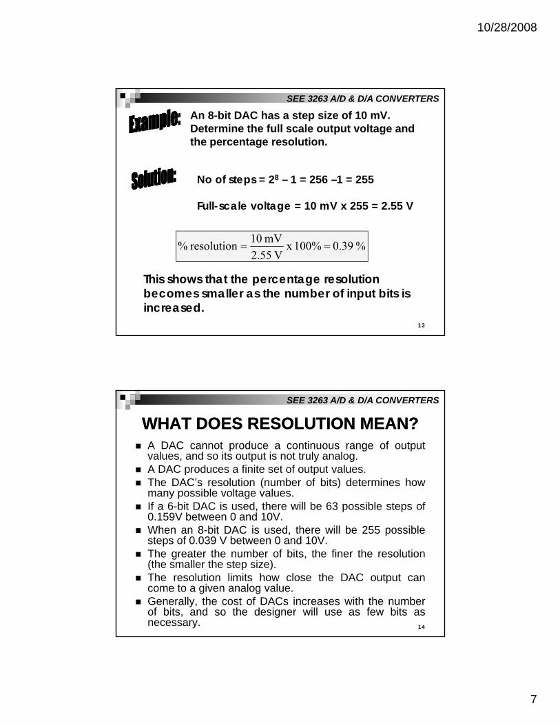
BCD INPUT CODEBCD INPUT CODEThe DACs we have considered thus far have used a binary input code.Many DACs use a BCD input code where 4-bit code groups are used for each decimal digit.
204080D1
C1B1
BCD for MSD
DAC10
1248
A1
D0C0B0A0
BCD for LSD
Vout 100 possible values since input ranges from 00 to 99
Step size = weight of A0
15
SEE 3263 A/D & D/A CONVERTERS
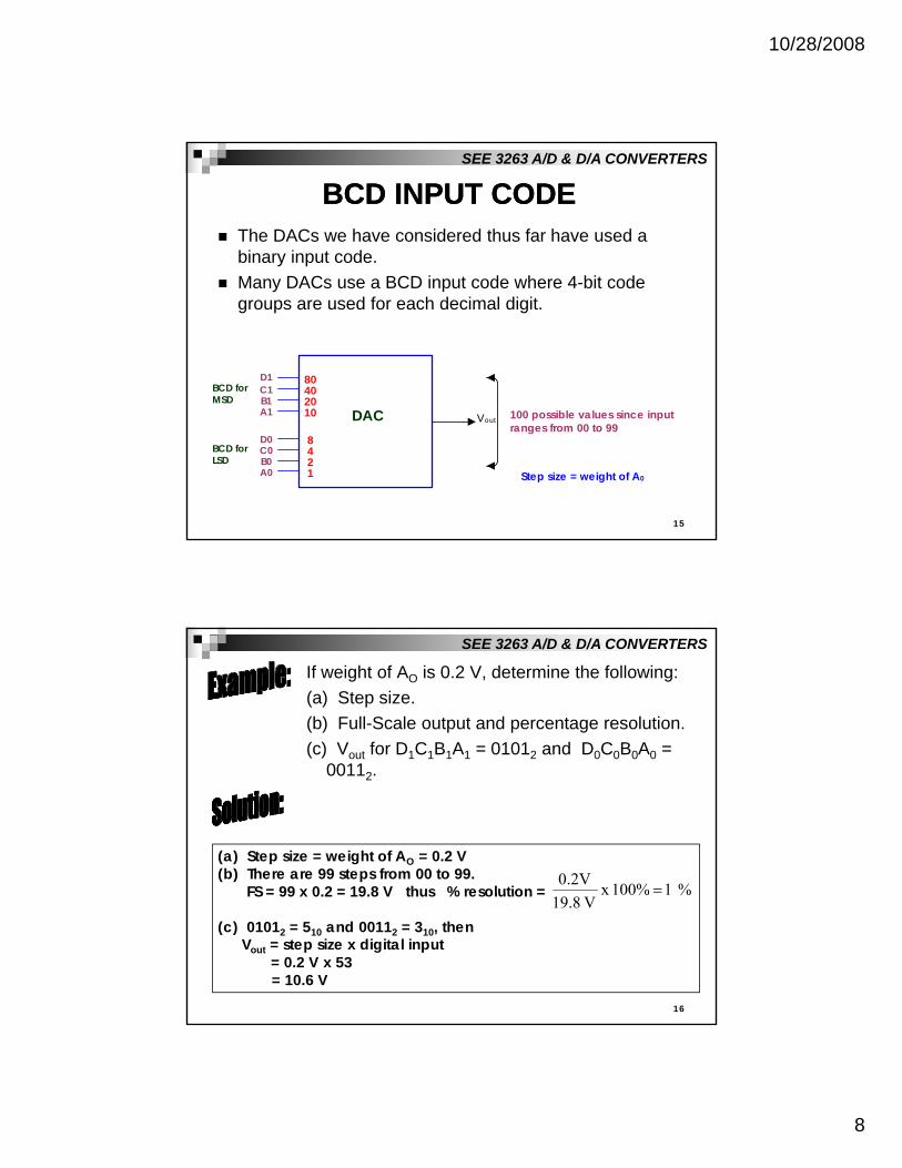
If weight of AO is 0.2 V, determine the following:(a) Step size.(b) Full-Scale output and percentage resolution.(c) Vout for D1C1B1A1 = 01012 and D0C0B0A0 =
00112.
(a) Step size = weight of AO = 0.2 V(b) There are 99 steps from 00 to 99.
FS = 99 x 0 2 = 19 8 V thus % resolution = %1100%x.2V0=FS = 99 x 0.2 = 19.8 V thus % resolution =
(c) 01012 = 510 and 00112 = 310, then Vout = step size x digital input
= 0.2 V x 53 = 10.6 V
% 1 100%x V19.8
16

10/28/2008
9
SEE 3263 A/D & D/A CONVERTERS
DIGITALDIGITAL--TOTO-- ANALOG CONVERTERANALOG CONVERTER
There are 2 types of typical DAC converterThere are 2 types of typical DAC converter circuit:
DAC binary weighted
DAC R – 2R ladder network
17
SEE 3263 A/D & D/A CONVERTERS
Binary Weighted DAC Binary Weighted DAC This is the basic circuit for one type of 4-bit DAC. The inputs are bi i t hi h d t binary input which are assumed to have values of either 0V or 5V.
The op-amp is employed as a summing amplifier, which produces the weighted sum of these input voltages.
The output is evaluated for any RV I ,
2RV I ,
4RV I ,
8RV I D
3C
2B
1A
O ====p y
input condition by setting the appropriate inputs to either 0V or 5V. For example, if the digital input is 10102, then VD = VB = 5V and VC = VA = 0V. Thus VOUT = -(V+0+1/4V+0) = 6.25V ⎟
⎠⎞
⎜⎝⎛ +++−=
−=
DF
CF
BF
AF
FFO
VRR V
2RR V
4RR V
8RRRIV
R, 2R, 4R, 8R refer to the weighted of 23, 22, 21 and 20. Thus
18

10/28/2008
10
SEE 3263 A/D & D/A CONVERTERS
How close the circuit comes to producing an accurate values depends primarily on two factors:
The precision of the input and feedback resistors.
The precision of the input voltage levelsThe precision of the input voltage levels.
19
SEE 3263 A/D & D/A CONVERTERS
PRECISION REFERENCE PRECISION REFERENCE SUPPLYSUPPLY
VRef
IO IO/2 IO/4 IO/8Use semiconductor
-
+
R 2R 4R 8RRF
IF= IO
IO VOSwitch closed when input bit = 1
switch like the CMOS transmission gate
B3 B2 B1 B0
MSB LSB
RVWhere I
8IB
4IB
2IBIBI
REFO
O0
O1
O2O3O
=
×+×+×+×=
20

10/28/2008
11
SEE 3263 A/D & D/A CONVERTERS
RR--2R LADDER NETWORK2R LADDER NETWORK
4-bit R-2R is constructed with 3 constructed with 3 resistors R and 5 resistors 2R. Normally R = 10 kΩand 2R = 20 kΩ.
4 current switches ill b ti t d will be activated
depends on the digital input.
input)D(digital )21)(
RV(
16I
)input digitalD(Bcurrent LSI
4REFO
out
×==
×=
21
SEE 3263 A/D & D/A CONVERTERS
DAC OUTPUT VOLTAGEDAC OUTPUT VOLTAGEIn general, for n-bit,
21
RVI n
REF)LSB(O ⎟
⎠⎞
⎜⎝⎛⎟⎠⎞
⎜⎝⎛=
V I R ( t LSB) R DVO = -IoutRF = -(current LSB) x RF x D
Voltage Resolution = voltage LSB =
Therefore VO = -(voltage resolution) x D
FnREF R R
V⎟⎠⎞
⎜⎝⎛⎟⎠⎞
⎜⎝⎛
21
22

10/28/2008
12
SEE 3263 A/D & D/A CONVERTERS
Assume VREF = 10 V for 4-bit R-2R withR = 10kΩ. Determine:(a) Current resolution.(b) IO when the digital input is 11112
(a) n = 4
A0 06251V101VIl i REF ⎞⎜⎛⎞
⎜⎛⎞
⎜⎛⎞
⎜⎛
(b) IO = 1O(LSB) x D = (0.0625 mA) (15) = 0.9375 mA
mA 0.062521
k10V10
21
RVIresolution 4n
REF)LSB(O =
⎠⎞
⎜⎝⎛⎠⎞
⎜⎝⎛
Ω=
⎠⎞
⎜⎝⎛⎠⎞
⎜⎝⎛==
23
SEE 3263 A/D & D/A CONVERTERS
DAC INTEGRATED CIRCUITDAC INTEGRATED CIRCUIT(DAC 0808/ MC1408)(DAC 0808/ MC1408)
24
10/28/2008
13
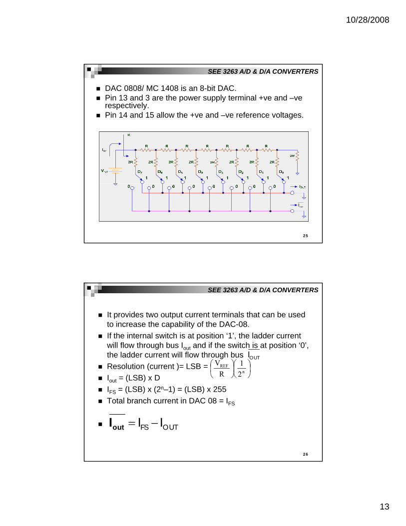
SEE 3263 A/D & D/A CONVERTERS
DAC 0808/ MC 1408 is an 8-bit DAC.Pin 13 and 3 are the power supply terminal +ve and –ve respectively.Pin 14 and 15 allow the +ve and –ve reference voltages.
outI
25
SEE 3263 A/D & D/A CONVERTERS
It provides two output current terminals that can be used to increase the capability of the DAC-08.If the internal switch is at position ‘1’, the ladder current
ill fl h h b I d if h i h i i i ‘0’will flow through bus Iout and if the switch is at position ‘0’, the ladder current will flow through busResolution (current )= LSB =Iout = (LSB) x DIFS = (LSB) x (2n–1) = (LSB) x 255Total branch current in DAC 08 = IFS
21
RV
nREF ⎟
⎠⎞
⎜⎝⎛⎟⎠⎞
⎜⎝⎛
OUTI
Total branch current in DAC 08 IFS
OUTFS II −=outI
26

10/28/2008
14
SEE 3263 A/D & D/A CONVERTERS
R0 1 F
-15 V +15 V
UNIPOLAR ANALOG OUTPUT UNIPOLAR ANALOG OUTPUT VOLTAGEVOLTAGE
-
+Vref
Rref
Iref
IOUT
outI
RF
5
133
21121110976 8
4
0.1 F0.1 F0.1 F
1614
15
DAC -082
3 6
-15 V
+15 V
+10 V
5 K
5 K
5 K
MSB LSB
Vo= IoutRF
D1D2D3 D0D4D5D6D7
D sulotion voltage reV
R21
RVsolutionVoltage re
O
FnREF
×=
×⎟⎠⎞
⎜⎝⎛⎟⎠⎞
⎜⎝⎛=
27
SEE 3263 A/D & D/A CONVERTERS
-
+Vref
Rref
Iref
IOUT
outI
RF
5
133
21121110976 8
4
0.1 F0.1 F0.1 F
1614
15
DAC -082
3 6
-15 V +15 V
15 V
+15 V
+10 V
5 K
5 K
MSB LSB
Vo= IoutRF
For unipolar DAC-08, determine VO for the following inputs:(a) 00000001 (b) 11111111
D1D2D3 D0D4D5D6D7
-15 V5 K
(a) 000000012 (b) 111111112
mV 39kΩ521
kΩ5V10R
21
RVV 8Fn
REFLSB =×⎟
⎠⎞
⎜⎝⎛⎟⎠⎞
⎜⎝⎛=×⎟
⎠⎞
⎜⎝⎛⎟⎠⎞
⎜⎝⎛=
(a) VO = VLSB x D = 39 mV x 1 = 39 mV(b) VO = VLSB x D = 39 mV x 255 = 9.961 V 28

10/28/2008
15
SEE 3263 A/D & D/A CONVERTERS
BIPOLAR ANALOG OUTPUT BIPOLAR ANALOG OUTPUT VOLTAGEVOLTAGE
outI FoutO R)I(V outI−=
FoutO R)I(V outI−= )II( outFS −=outI
29
SEE 3263 A/D & D/A CONVERTERS
For bipolar DAC-08, determine VO for an input of 011111112
A 821
kΩ5V24.10
21
RVsolutionCurrent re 8n
REF µ=⎟⎠⎞
⎜⎝⎛⎟⎠⎞
⎜⎝⎛=⎟
⎠⎞
⎜⎝⎛⎟⎠⎞
⎜⎝⎛=
IFS = 8µA x 255 = 2.04mAFS µIout = 8µA x 12710 = 1.016mA ,
VO = (1.016mA - 1.024mA)x5kΩ = - 0.04 V
mA024.1mA016.1mA04.2Iout
=−=
30

10/28/2008
16
SEE 3263 A/D & D/A CONVERTERSoutI
For bipolar DAC-08 determine Vo for the following inputs: (a) 000000002 (b) 011111112
(c) 100000002 (d) 111111112
Current resolution = = = 8µAIFS = 8µA X 255 = 2.04mAIout = 8µA x 0 = 0, Vo = (0 - 2.04mA)5KΩ = -10.2 V
N t th t th f ll l lt h h th i t i 0 d
21
RV
nREF ⎟
⎠⎞
⎜⎝⎛⎟⎠⎞
⎜⎝⎛
6521
5K10.24
⎟⎠⎞
⎜⎝⎛⎟⎠⎞
⎜⎝⎛
Note that the –ve full-scale voltage happen when the input is 0 and the +ve full-scale voltage happen when all inputs are 1.
31
Digital Input Analog OutputD7 D6 D5 D4 D3 D2 D1 D0 Iout(mA) (mA) Vo(V)
-ve full-scaleNegative zeroPositive zero+ve full-scale
0 0 0 0 0 0 0 00 1 1 1 1 1 1 11 0 0 0 0 0 0 01 1 1 1 1 1 1 1
01.016 1.024 2.04
2.041.0241.016
0
-10.2-0.0400.04010.2
outI
SEE 3263 A/D & D/A CONVERTERS
An 8-bit DAC has a full scale output of 2 mA and a full scale error ± 0.5 %. What are the possible output range for an input of 100000002.2
Step size= 2 mA/255 = 7.84 µAInput 100000002 = 12810Ideal output current = ILSB x D = 7.84 µA x 128 = 1004 µALSBMaximum error = ± 0.5 % x 2 mA = ± 10 µAThus an ideal output current range = 1004 µA ± 10 µA = 994 µA to 1014 µA
32

10/28/2008
17
SEE 3263 A/D & D/A CONVERTERS
ANALOGANALOG--TOTO--DIGITAL DIGITAL CONVERTER (ADC)CONVERTER (ADC)
An ADC takes an analog input voltage and after a t i t f ti d di it l t t dcertain amount of time produces a digital output code
which represents the analog input.
33
SEE 3263 A/D & D/A CONVERTERS
Digital Ramp ADC Digital Ramp ADC
34

10/28/2008
18
SEE 3263 A/D & D/A CONVERTERS
For a digital ramp ADC if f = 1 MHz V =For a digital ramp ADC, if fclk = 1 MHz, VT = 0.1 mV, full-scale output = 10.23 V and a 10-bit input, determine:
The digital equivalent obtained for VA = 3.728 V.The conversion time.The resolution of this converter.
35
SEE 3263 A/D & D/A CONVERTERS
Total possible steps = 210 – 1 = 102310
Step size = mV101023
23.10=p
Since VA = 3.728 V and VT = 0.1 mVVAX must reach 3.7281 VThis needs
1023
steps 373 372.81 mV10
V 7281.3==
37310 = 01011101012
Require 373 steps to complete the conversion, so need 373 clock pulses = 373 µs = tcresolution = step size = 10 mV
36

10/28/2008
19
SEE 3263 A/D & D/A CONVERTERS
SUCCESSIVE APPROXIMATION SUCCESSIVE APPROXIMATION ADC (SAC)ADC (SAC)
37
SEE 3263 A/D & D/A CONVERTERS
START
Clear all bits
Start at
Assume a 4-bit SAC with a step size of 1V.Let assume the
l i t MSB
Set bit = 1
Clear bit back to 0
ISVAX > VA ?
Have
Yes
No
No
analog input, VA=10.4V
all bits beenchecked?
Go to nextlowest bit
Conversion is complete and result is in REGISTER
Yes
END38
10/28/2008
20
SEE 3263 A/D & D/A CONVERTERS
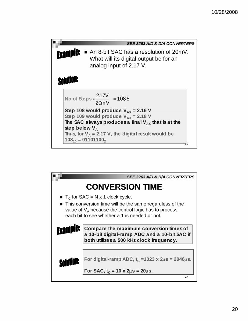
An 8-bit SAC has a resolution of 20mV. What will its digital output be for an analog input of 2.17 V.
No of Steps =
Step 108 would produce VAX = 2.16 V
5.108 mV20
V17.2=
Step 108 would produce VAX 2.16 VStep 109 would produce VAX = 2.18 VThe SAC always produces a final VAX that is at the step below VAThus, for VA = 2.17 V, the digital result would be 10810 = 011011002
39
SEE 3263 A/D & D/A CONVERTERS
CONVERSION TIMECONVERSION TIMETC for SAC = N x 1 clock cycle.This conversion time will be the same regardless of the value of V because the control logic has to processvalue of VA because the control logic has to process each bit to see whether a 1 is needed or not.
Compare the maximum conversion times of a 10-bit digital-ramp ADC and a 10-bit SAC if both utilizes a 500 kHz clock frequency.
For digital-ramp ADC, tC =1023 x 2µs = 2046µs.
For SAC, tC = 10 x 2µs = 20µs.40

10/28/2008
21
SEE 3263 A/D & D/A CONVERTERS
THE ADC0804 INTEGRATED THE ADC0804 INTEGRATED CIRCUIT CIRCUIT
It is an 8-bit ADC that performs A/D conversion using the successive-approximation method.It has two analog inputs: VIN(+) and VIN(-) to allow differential inputs.The actual analog input, VIN = VIN(+) - VIN(-).In single-ended measurements, the analog input is
li d t V ( ) hil V ( ) i t d t lapplied to VIN(+) while VIN(-) is connected to analog ground.During normal operation, the converter uses VCC = + 5V as its reference voltage, and the analog input can range from 0 to 5V full scale.
41
SEE 3263 A/D & D/A CONVERTERS
With 8-bits, the resolution is =
It has an internal clock generator circuit that produces a frequency of 1
mV 19.6 255
V 5=
frequency of
where R and C are values of externally connected components.A typical clock frequency is 606 kHz using R = 10 kΩand C = 150 pF. If desired, an external clock frequency
RC1.11f =
can be used by connecting it to the CLK IN pin.With 606kHz clock frequency, TC = 13.2µs.It has separate ground connections for digital and analog voltages at pin 10 and pin 8 respectively.
42
10/28/2008
22
SEE 3263 A/D & D/A CONVERTERS
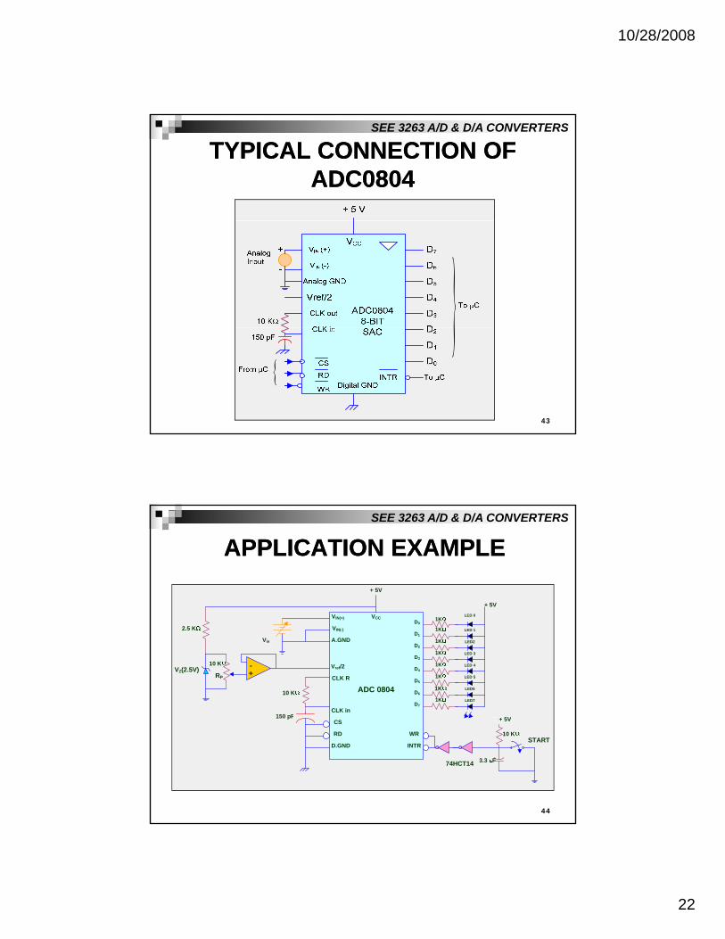
TYPICAL CONNECTION OF TYPICAL CONNECTION OF ADC0804 ADC0804
43
SEE 3263 A/D & D/A CONVERTERS
APPLICATION EXAMPLEAPPLICATION EXAMPLE
+ 5V
+ 5V
LED 0VCCVIN(+)
VIN(-)
A.GND
Vref/2
CLK R
CLK in
Vin
10 K
150 pF
1K
1K
1K
1K
1K
1K
1K
ADC 08041K
5V
D0
D1
D2
D3
D4
D5
D6
D7
LED 1
+-
2.5 K
VZ(2.5V)10 K
RP
LED2
LED 3
LED 4
LED 5
LED6
LED7
CS
RD
D.GND
150 pF + 5V
INTR
WR 10 K
3.3 F
START
74HCT14
44

10/28/2008
23
SEE 3263 A/D & D/A CONVERTERS
Referring to the figure above, RP is the 10 kΩpotentiometer. If RP is set so that V+ = 1.28 V, determine:
The input voltage range Vin
The voltage resolutionThe conversion timeThe LED that will light up when Vin = 2.26 VThe input voltage when the digital output is 10101112
45
SEE 3263 A/D & D/A CONVERTERS
V56.2VV28.1V2
Vref
ref =⇒== +
mV0410V56.2resolutionvoltage
Input voltage range Vin = 0 V hingga 2.56 V
mV04.10255
resolution voltage ==
1.22526.2stepsTotal ==
T = 1.1 RC = 1.1 x 10kΩ x 150pF = 1.65 µsTherefore tc = N x T = 8 x 1.65 µs = 13.2 µsWhen Vin = 2.26 V
46
1.225mV04.10
steps Total
Thus total steps = 22510 = 111000012=D7D6D5D4D3D2D1D0LED that will light up: LED4, LED3, LED2, LED1Vin = 8710 x 10.04mV = 0.8735V although actual Vinshould be slightly greater than 0.8735V.
10/28/2008
24
SEE 3263 A/D & D/A CONVERTERS
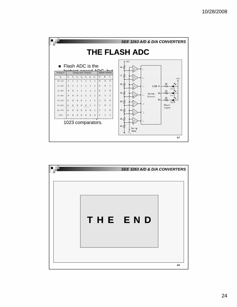
THE FLASH ADCTHE FLASH ADCFlash ADC is the highest-speed ADC, butA l i C t O t t Di it l O t thighest speed ADC, but it requires much more circuitry.For example, a 6-bit flash ADC requires 63 analog comparators, while an 8-bit unit requires 255
Analog in Comparator Outputs Digital Outputs
VA C1 C2 C3 C4 C5 C6 C7 A B C
0 – 1 V
1 – 2 V
2 – 3 V
3 – 4 V
4 – 5 V
5 – 6 V
1 1 1 1 1 1 1
0 1 1 1 1 1 1
0 0 1 1 1 1 1
0 0 0 1 1 1 1
0 0 0 0 1 1 1
0 0 0 0 0 1 1
0 0 0
0 0 1
0 1 0
0 1 1
1 0 0
1 0 1requires 255 comparators, and a 10-bit converter requires 1023 comparators.
47
6 – 7 V
>7 V
0 0 0 0 0 0 1
0 0 0 0 0 0 0
1 1 0
1 1 1
SEE 3263 A/D & D/A CONVERTERS
T H E T H E EE N DN D
48