Selecting Analog-to-Digital Converters
26
ADCBRIEF.CDR TJS 4/20/96 Page 1 Selecting Analog-to-Digital Converters For Data Acquisition: An Overview of Test Methodologies by Tim J. Sobering April 29, 1996 Copyright 1996 Tim J. Sobering
-
Upload
independent -
Category
Documents
-
view
3 -
download
0
Transcript of Selecting Analog-to-Digital Converters

ADCBRIEF.CDRTJS 4/20/96Page 1
Selecting Analog-to-Digital ConvertersFor
Data Acquisition:
An Overview of Test Methodologies
byTim J. Sobering
April 29, 1996
Copyright 1996Tim J. Sobering
l
l
l
l
l
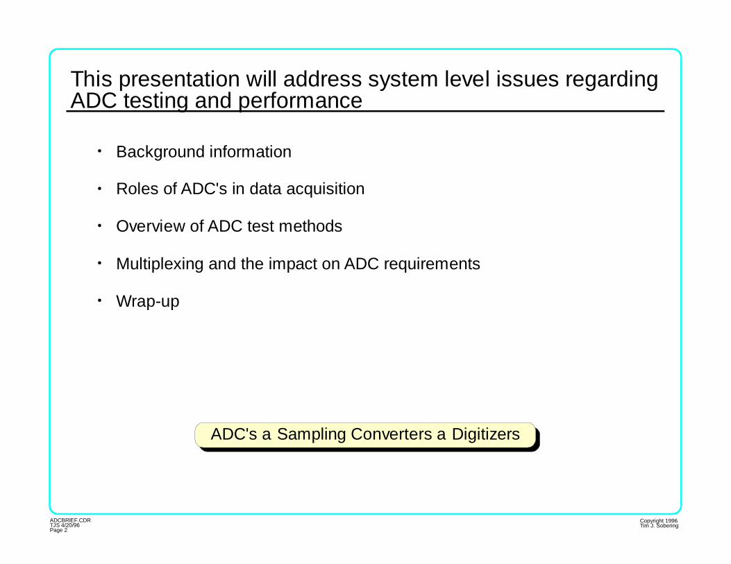
This presentation will address system level issues regardingADC testing and performance
ADCBRIEF.CDRTJS 4/20/96Page 2
Background information
Roles of ADC's in data acquisition
Overview of ADC test methods
Multiplexing and the impact on ADC requirements
Wrap-up
ADC's Sampling Converters Digitizersa a
Copyright 1996Tim J. Sobering
l
l
l
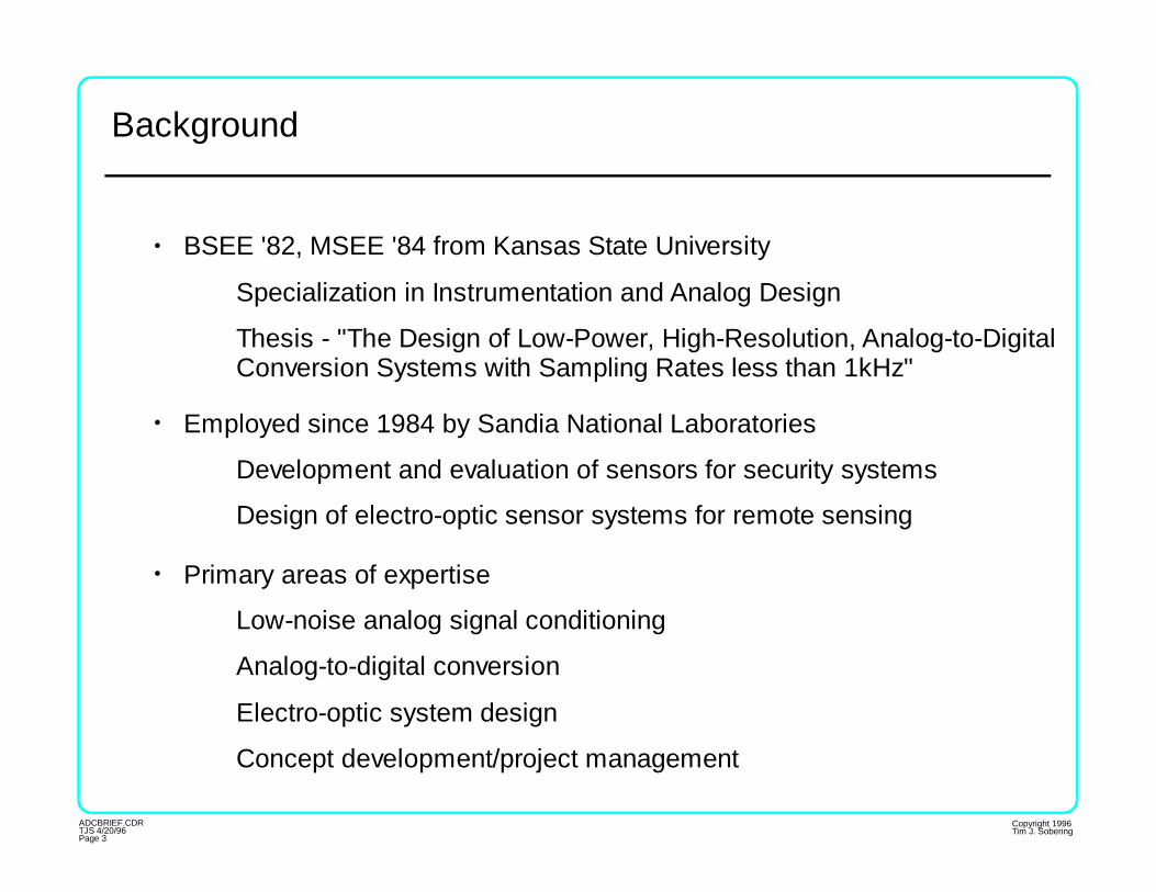
Background
ADCBRIEF.CDRTJS 4/20/96Page 3
BSEE '82, MSEE '84 from Kansas State University
Specialization in Instrumentation and Analog Design
Thesis - "The Design of Low-Power, High-Resolution, Analog-to-DigitalConversion Systems with Sampling Rates less than 1kHz"
Employed since 1984 by Sandia National Laboratories
Development and evaluation of sensors for security systems
Design of electro-optic sensor systems for remote sensing
Primary areas of expertise
Low-noise analog signal conditioning
Analog-to-digital conversion
Electro-optic system design
Concept development/project management
Copyright 1996Tim J. Sobering

l
l
l
l
l
Sandia National Laboratories has served as aPrime Contractor to the DOE for over 40 years
ADCBRIEF.CDRTJS 4/20/96Page 4
Sandia is a government-owned contractor-operated (GOCO) facility.
Currently Lockheed Martin manages Sandia.
Sandia's principal function is weapons research and development andmaintenance of the Nation's nuclear stockpile (~60%).
Sandia has broadened its mission to include such areas as:Energy ResearchSafeguards and SecurityEnvironmental RestorationTreaty Monitoring
Microelectronics and PhotonicsRoboticsSupercomputing
Sandia currently employs approximately 7500 people in Albuquerque, NM,and 900 people in Livermore, CA.
Copyright 1996Tim J. Sobering
l
l
l
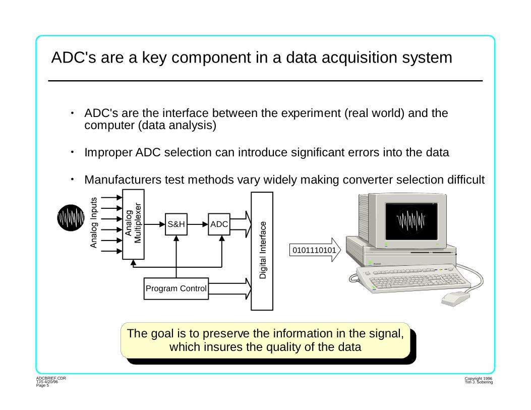
ADC's are a key component in a data acquisition system
ADCBRIEF.CDRTJS 4/20/96Page 5
ADC's are the interface between the experiment (real world) and thecomputer (data analysis)
Improper ADC selection can introduce significant errors into the data
Manufacturers test methods vary widely making converter selection difficult
The goal is to preserve the information in the signal,which insures the quality of the data
0101110101
Program Control
ADCS&H
Copyright 1996Tim J. Sobering

l
l
l
ADC's are typically operated in one of three modes
ADCBRIEF.CDRTJS 4/20/96Page 6
DC (low-frequency) Conversion
Signal is "stable" between samples and during acquisition
Examples: digital voltmeters, temperature probes
Signal Reconstruction
Conditions of the Sampling Theorem are met
Example: CD audio, frequency analysis
Time-multiplexed Operation
Multiple signal sources are digitized using a single ADC
Examples: data logging, CCD arrays
Copyright 1996Tim J. Sobering

l
l
Two classes of tests are used for characterizing ADC's
ADCBRIEF.CDRTJS 4/20/96Page 7
Static Testing
Effectively a DC input signal
Good for gross characterization of devices
Not representative of the mode of operation of most ADC's
Dynamic Testing
Usually a sinusoidal input signal
Multiple tests have been developed to measure different parameters
Results directly applicable to devices operated in SignalReconstruction Mode
Tests do not address multiplexed operation
Copyright 1996Tim J. Sobering

Dynamic testing reveals errors not detected in static tests
ADCBRIEF.CDRTJS 4/20/96Page 8
Static Testing Dynamic Testing
The performance of an ADC is very dependenton the slew rate of the signal being digitized
Copyright 1996Tim J. Sobering
Figures from Reference 1
l
l
l
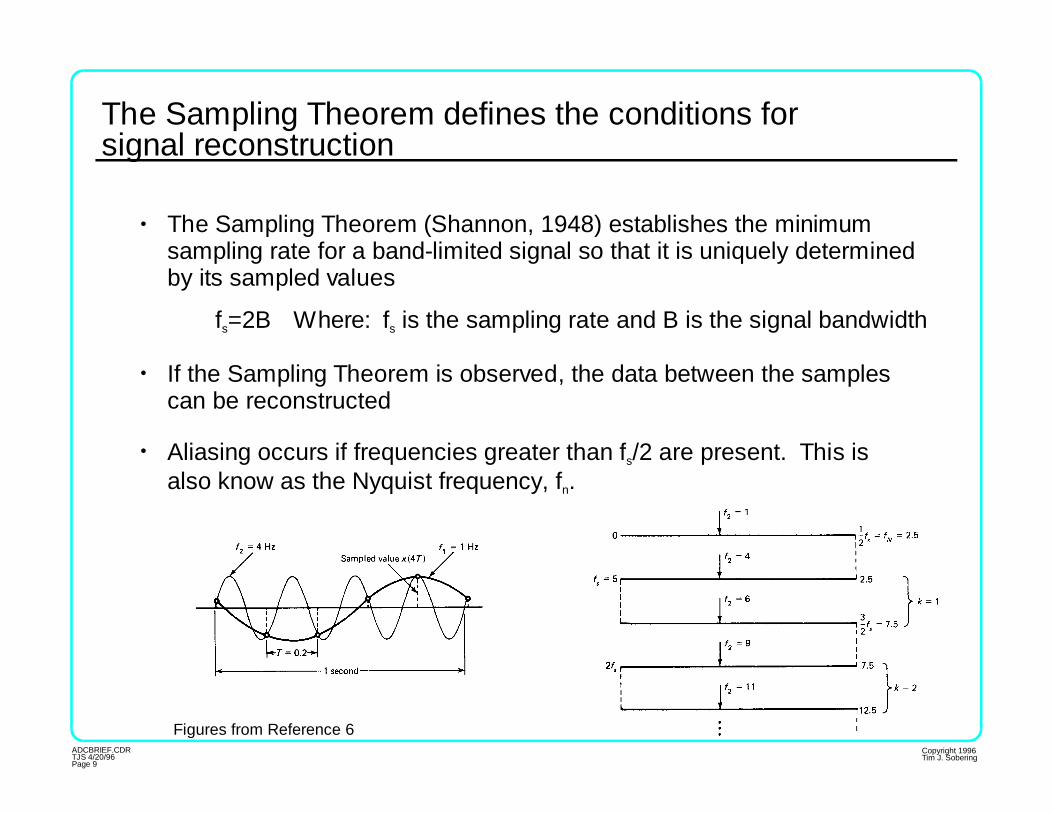
The Sampling Theorem defines the conditions forsignal reconstruction
ADCBRIEF.CDRTJS 4/20/96Page 9
The Sampling Theorem (Shannon, 1948) establishes the minimumsampling rate for a band-limited signal so that it is uniquely determinedby its sampled values
f =2Bs f is the sampling rate and B is the signal bandwidthsWhere:
If the Sampling Theorem is observed, the data between the samplescan be reconstructed
Aliasing occurs if frequencies greater than f /2 are present. This isalso know as the Nyquist frequency, f .
s
n
Copyright 1996Tim J. Sobering
Figures from Reference 6

l
l
l
l
No single test method measures all ADC parameters
ADCBRIEF.CDRTJS 4/20/96Page 10
Fast Fourier Transfer Test
Histogram Test
Sine Wave Curve Fit
Beat Frequency Test - gross characterization
Other tests
Envelope Test - stringent test of settling time (Nyquist limited)
Integral nonlinearity (INL), signal-to-noise ratio (SNR)
Differential nonlinearity (DNL), missing codes, gain and offset errors
Total rms error and effective number of bits (ENOB)
Copyright 1996Tim J. Sobering

l
l
l
l
Fast Fourier Transform test
ADCBRIEF.CDRTJS 4/20/96Page 11
Digitize a spectrally pure near full-scale sinusoid and compute the FFT
Measures INL and SNR of device
Advantages:
Small number of samples required (typically 1024)
Disadvantages:
Small number of ADC codes exercised in high resolution ADC's
Differential nonlinearity, aperture uncertainty, and system noiseare lumped together
Fast
Spectrally pure test signal can be difficult to generate for fast ADC's
Very sensitive to test signal noise
Copyright 1996Tim J. Sobering

l
l
FFT test examples
ADCBRIEF.CDRTJS 4/20/96Page 12
FFT plots for a 20 MHz, 8-bit ADC with input frequencies of 0.95 MHzand 9.85 MHz
Note increase in harmonic distortion indicating significant INLat higher slew rates
Copyright 1996Tim J. Sobering
Figures from Reference 1

l
l
l
l
Histogram test
ADCBRIEF.CDRTJS 4/20/96Page 13
Drive the input of the ADC with a full-scale sinusoid and plot the histogram
Best method of measuring DNL
Advantages:
Large number of samples required (19.8 million for 15-bit ADCmeasuring to 95% confidence)
Disadvantages:
Temporal and thermal variations of test equipment and DUTcan cause errors (above example would take 5.5 hours at 1 kHz)
Number of occurrences vs. output code
Also yields missing codes, gain and offset errors
Less sensitive to noise in test signal
Copyright 1996Tim J. Sobering

Histogram test examples
ADCBRIEF.CDRTJS 4/20/96Page 14
20 MHz, 10-bit ADC with small DNL 20 MHz, 8-bit ADC with large DNLand missing codes
Copyright 1996Tim J. Sobering
Figures from Reference 1

l
l
l
l
Sine Wave Curve Fit
ADCBRIEF.CDRTJS 4/20/96Page 15
All error sources are rolled together -- devices with identicalENOB may respond differently, depending on the application
Disadvantages:
Yields total rms error and effective number of bits (ENOB)
Digitize a spectrally pure 90% full-scale sinusoid and fit an ideal sinusoidto the data using least-squares minimization
Compare the rms error between the actual and ideal signals withthe rms error from an ideal quantizer of equal resolution
Advantages:
ENOB is a pseudo-standard for comparing devices
Accurate test signal may be difficult to generate, especially forhigh-speed ADC's
Copyright 1996Tim J. Sobering

l
l
l
Conventional dynamic test methods may not predictmultiplexed device performance
ADCBRIEF.CDRTJS 4/20/96Page 16
Conventional dynamic testing assumes that signals above the Nyquistfrequency have been eliminated
Multiplexed operation is unique in that the ADC must track signals wellin excess of the Nyquist frequency
Manufacturers often omit full-power bandwidth from specifications
Multiplexed operation requires test methodology which evaluatesinput amplifier and sample-and-hold bandwidth, slew rate, and stability.
Copyright 1996Tim J. Sobering

l
l
l
Simple multiplexing can stress ADC performance
ADCBRIEF.CDRTJS 4/20/96Page 17
Multiplexing can result in a full-scale signal change in one sample period
3V
5V
+5V
-5V
-5V
-2V
M
U
X
A
D
C
Ts
∆V
Analysis shows that the ADC bandwidth and slew rate must increasesignificantly over the sinusoidal signal case
Resolution Bandwidth Slew Rate
8 bits
12 bits
16 bits
2.0 x fn
2.9 x fn
3.8 x fn
4 x f sinusoidn
5.7 x f sinusoidn
7.5 x f sinusoidn
Fortunately, this mode of operation typically uses a low sample rate
Copyright 1996Tim J. Sobering

l
l
The readout of a multiplexed diode array further stressesthe ADC's dynamic performance
ADCBRIEF.CDRTJS 4/20/96Page 18
Requirement to settle pixel value and kTC offset cuts available settlingtime by a factor of two
Cp Cp Cp
Cv
Video Line
Reset
Reset Bias
Substrate
Shift RegisterPhase 1Phase 2Start
Time (microseconds)
0 2 4 6 8 10 12-0.25
-0.20
-0.15
-0.10
-0.05
0.00
0.05
0.10
Pixeln
Pixeln+1
Pixeln-1
CDS
Reset
CDS
Reset Reset
CDS
ADC Sample
Schematic of a Reticon M-series linear array M-series array output measured at preamplifier
Inclusion of a sample-and-hold simply shifts the problem
Copyright 1996Tim J. Sobering

l
l
Analog post-processing may not help the problem
ADCBRIEF.CDRTJS 4/20/96Page 19
Slew rates can increase due to signal amplification
CCDS
vCDS
CDS
To ADCFrom Array G1 G2
+ -
Time (microseconds)
0 2 4 6 8 10 12
-10.00
-8.00
-6.00
-4.00
-2.00
0.00
Pixel n
Pixel n+1
Pixel n-1
CDS
Reset
CDS
Reset
Reset
CDS
ADC Sample
CDS signal conditioning circuit M-series array output measured at ADC input
Bandwidth limiting may reduce overdrive on ADC input stage
Copyright 1996Tim J. Sobering

ADC Simple Multiplexing Photodiode ReadoutResolution
(N)MinimumBandwidth
MinimumSlew Rate
MinimumBandwidth
MinimumSlew Rate
8 1.99 fN 12.5 fN ∆V 4.0 fN 25.0 fN ∆V10 2.43 fN 15.3 fN ∆V 4.9 fN 30.5 fN ∆V12 2.87 fN 18.0 fN ∆V 5.7 fN 36.0 fN ∆V16 3.75 fN 23.6 fN ∆V 7.5 fN 47.1 fN ∆V
l
l
Array readouts represent a "worst case" because speedand resolution requirements are typically high
ADCBRIEF.CDRTJS 4/20/96Page 20
The following table shows a comparison of the bandwidth and slew raterequirements for the two multiplexing cases
ADC Simple Multiplexing Photodiode ReadoutResolution
(N)MinimumBandwidth
MinimumSlew Rate
MinimumBandwidth
MinimumSlew Rate
8 1.99 fN 12.5 fN ∆V 4.0 fN 25.0 fN ∆V10 2.43 fN 15.3 fN ∆V 4.9 fN 30.5 fN ∆V12 2.87 fN 18.0 fN ∆V 5.7 fN 36.0 fN ∆V16 3.75 fN 23.6 fN ∆V 7.5 fN 47.1 fN ∆V
The maximum slew rate of a sinusoid at the Nyquist frequencyis given by f Vπ ∆n
Copyright 1996Tim J. Sobering

l
The effect of slew rate and bandwidth can be seenin ENOB plots
ADCBRIEF.CDRTJS 4/20/96Page 21
ENOB decrease with increasing frequency is due to limited slew rateand gain errors resulting from insufficient bandwidth
Input Frequency
Copyright 1996Tim J. Sobering

l
l
l
How can an ADC be tested for use in a multiplexed mode?
ADCBRIEF.CDRTJS 4/20/96Page 22
Envelope Test is representative of simple multiplexing case
Conventional dynamic tests do not stress performance
"Contrast Test" is proposed for array readout applications
A near Nyquist frequency sinusoid is used to force sampling ofalternating phases of the input signal
Copyright 1996Tim J. Sobering
Figures from Reference 1
l
l
There are several global requirements for ADC's used inelectronic imaging applications
ADCBRIEF.CDRTJS 4/20/96Page 23
The ADC must preserve discontinuities (edges or contrast)
The ADC must not introduce discontinuities where none exist
This is less important for viewing by a person because the eye isan excellent edge detector
This is a measure of the DNL and is important in preserving theaesthetic quality of the image (pleasing to the eye)
This is very important for machine vision and imaging radiometryapplications so that the scene contrast and the pixel radiance areaccurately measured
Copyright 1996Tim J. Sobering

l
l
l
The contrast test simulates the multiplexed array application(electronic imaging)
ADCBRIEF.CDRTJS 4/20/96Page 24
Input and output data are compared to measure DNL and step response
A variable amplitude, variable phase square wave is used as thetest signal
DAC ADC
Computer
ADCSample
DACOutput
DAC performance is critical and must exceed ADC performance
Copyright 1996Tim J. Sobering

l
l
l
l
Summary
ADCBRIEF.CDRTJS 4/20/96Page 25
Static testing is of limited value
ADC selection is critical in preserving data quality
Dynamic testing will predict performance in signal reconstruction mode
New test methods are needed for testing ADC's used in multiplexed mode
Consider the application when selecting ADC test methods
Copyright 1996Tim J. Sobering

References
ADCBRIEF.CDRTJS 4/20/96Page 26
Hewlett Packard Corporation,, Product Note 5180A-2.
D.W. Doerfler, ,SAND 85-7250, Sandia National Laboratories, 1985.
M. J. Demler,, , March 30, 1992, p. 115-120.
T.E. Linnenbrink, , ,vol. 33, no. 3, p.184-187, Sept. 1984.
C. Sabolis,, , pp. 119-126, October 1993.
N. Ahmed, , Reston PublishingCompany, Reston Va.
Dynamic Performance Testing of A to DConverters
Techniques for Testing a 15-Bit Data Acquisition System
Time-domain techniques enhance testing of high-speedADCs
Effective Bits: Is That All There Is?
Seeing Is Believing, A/D converters make the difference inimaging applications
Discrete-Time Signals and Systems
EDN
IEEE Trans. IM
Photonics Spectra
1.
2.
3.
4.
5.
6.
Copyright 1996Tim J. Sobering