ANALOG DEVICES lc2mos - Elektronikjk
16
ANALOG DEVICES lc 2 mos Analog I/O Port AD7774 FEATURES Four-Channel, 8-Bit, 3.6 fts ADC Three DACs with On-Chip Amplifiers: One 11-Bit, 8 us DAC Two 8-Bit, 4 i-is DACs Simultaneous/Independent Sampling of Input Channels Adjustable Span and Bias Voltage for Input Channels Adjustable Bias Voltage for Output Channels Operates from +5 V and +12 V Supplies APPLICATIONS HDD Dedicated Servo HDD Hybrid Servo Closed-Loop Servo Systems GENERAL DESCRIPTION The AD7774 is a complete analog I/O port comprising three DACs (two 8-bit and one 11-bit) with output amplifiers, four input channels, two track/hold amplifiers and an 8-bit ADC. It has versatile input and output signal-conditioning features which make it ideal for use in head-positioning servos in dedicated- only and combined dedicated/embedded disk systems and other closed-loop digital servo systems. The part contains four input channels, grouped in pairs. V^] and V A2 share a common track/hold amplifier, Track/Hold A, while V BJ and V B2 share Track/Hold B. Either single or double conversions can be performed. In single conversion mode, any one of the four input channels can be converted. In double con- version mode, either V A , and V R , or V AZ and V H , axe simulta- neously held by Track/Hold A and Track/Hold B, and the heid voltages are sequentially converted. The center point of the transfer function (the bias voltage) can be set for all input and output channels. This makes the AD7774 especially useful in disk drives, where only a positive supply rail is available, as it allows the analog input and output voltages to be referred to a point other than analog ground. In addition, the input span (the swing around the bias voltage) can be set for the input channels. The output span for all three channels is set by the on-chip reference. The AD7774 operates from +5 V and +12 V supplies. It is fab- ricated in Linear Compatible CMOS <LC'MOSj, an advanced, mixed technology process that combines precision bipolar cir- cuits with low power CMOS logic. The part is available in a 28- lead dual-in-line (DIP) package and in a 28-terminal plastic leaded chip carrier (PLCC) package. PRODUCT HIGHLIGHTS 1. The AD7774 contains a four-channel, 3.6 fis ADC with in- put signal conditioning and three DACs with output amplifi- ers and output signal conditioning, on a single chip. 2. The midpoint of the ADC transfer function, the input volt- age swing of the ADC and the midpoint output voltage of the DACs can be set by applying ground referenced control voltages. 3. The AD7774 interface timing is compatible with most mod- ern microcontrollers and digital signal processors. FUNCTIONAL BLOCK DIAGRAM -O O- DAC A Js 11-BIT REGISTER V DAC 4 * 4 * DAC B J\ e-Brr REGISTER V DAC * I DAC C •M 8-BIT REGISTER V DAC ^—o—1)—c^—i— 6> —ct-——— n m 2.5V INTERNAL REFERENCE AND INPUT REFERENCE CIRCUITRY CS RD WH ADO AD1 AD2 BUSY REV. A Information furnished by Analog Devices is believed to be accurate and reliable. However, no responsibility is assumed by Analog Devices for its use, nor for any infringements of patents or other rights of third parties which may result from its use- No license is granted by implication or otherwise under any patent or patent rights of Analog Devices. DBO DB7 o~ VSW!NG One Technology Way. P.O. Box 9106, Norwood, MA 02062-3106, U S A Tel: 617/329-4700 Fax: 617/326-8703 Twx: 710/394-6577 Telex: 924491 Cable: ANALOG NORWOODMASS
-
Upload
khangminh22 -
Category
Documents
-
view
6 -
download
0
Transcript of ANALOG DEVICES lc2mos - Elektronikjk

ANALOG DEVICES
lc2mos Analog I/O Port
A D 7 7 7 4 FEATURES Four-Channel, 8-Bit, 3.6 fts ADC Three DACs with On-Chip Amplifiers:
One 11-Bit, 8 us DAC Two 8-Bit, 4 i-is DACs
Simultaneous/Independent Sampling of Input Channels
Adjustable Span and Bias Voltage for Input Channels Adjustable Bias Voltage for Output Channels Operates from +5 V and +12 V Supplies
APPLICATIONS HDD Dedicated Servo HDD Hybrid Servo Closed-Loop Servo Systems
GENERAL DESCRIPTION The AD7774 is a complete analog I/O port comprising three DACs (two 8-bit and one 11-bit) with output amplifiers, four input channels, two track/hold amplifiers and an 8-bit ADC. It has versatile input and output signal-conditioning features which make it ideal for use in head-positioning servos in dedicated-only and combined dedicated/embedded disk systems and other closed-loop digital servo systems.
The part contains four input channels, grouped in pairs. V^] and VA2 share a common track/hold amplifier, Track/Hold A, while VBJ and VB2 share Track/Hold B. Either single or double conversions can be performed. In single conversion mode, any one of the four input channels can be converted. In double con-version mode, either VA, and VR, or VAZ and VH , axe simulta-
neously held by Track/Hold A and Track/Hold B, and the heid voltages are sequentially converted.
The center point of the transfer function (the bias voltage) can be set for all input and output channels. This makes the AD7774 especially useful in disk drives, where only a positive supply rail is available, as it allows the analog input and output voltages to be referred to a point other than analog ground. In addition, the input span (the swing around the bias voltage) can be set for the input channels. The output span for all three channels is set by the on-chip reference.
The AD7774 operates from +5 V and +12 V supplies. It is fab-ricated in Linear Compatible CMOS <LC'MOSj, an advanced, mixed technology process that combines precision bipolar cir-cuits with low power CMOS logic. The part is available in a 28-lead dual-in-line (DIP) package and in a 28-terminal plastic leaded chip carrier (PLCC) package.
PRODUCT HIGHLIGHTS 1. The AD7774 contains a four-channel, 3.6 fis ADC with in-
put signal conditioning and three DACs with output amplifi-ers and output signal conditioning, on a single chip.
2. The midpoint of the ADC transfer function, the input volt-age swing of the ADC and the midpoint output voltage of the DACs can be set by applying ground referenced control voltages.
3. The AD7774 interface timing is compatible with most mod-ern microcontrollers and digital signal processors.
FUNCTIONAL BLOCK DIAGRAM
-O O-
DAC A Js 11-BIT REGISTER V
DAC
4 * 4 * DAC B J\ e-Brr
REGISTER V DAC
* I DAC C •M 8-BIT
REGISTER V DAC
—o—1)—c—i—6>—ct-———
n
m
2.5V INTERNAL REFERENCE AND
INPUT REFERENCE CIRCUITRY
CS RD WH ADO AD1 AD2 BUSY
REV. A In format ion furn ished by Analog Devices is bel ieved to be accurate and reliable. However, no responsibi l i ty is assumed by Analog Devices for its use, nor for any in f r ingements of patents or other r ights of th i rd parties which may result f rom its use- No license is granted by impl icat ion or otherwise under any patent or patent r ights of Ana log Devices.
DBO DB7 o~ VSW!NG
One Technology Way. P.O. Box 9106, Norwood, MA 02062-3106, U S A Tel: 617/329-4700 Fax: 617/326-8703 Twx: 710/394-6577 Telex: 924491 Cable: ANALOG NORWOODMASS

AD7774—SPECIFICATIONS ADO SPECIFICATIONS ( V M = + 1 0 V to + 1 3 . 2 V; V C £ = + 5 V ± 5 % : A G N D
stated. All specifications T(
D G N O = 0 V; V , + 5 V unless otherwise m „ to T m a i unless otherwise stated.)
Parameter K Version1 Units Conditions/Comments
DC ACCURACY Resolution2
Relative Accuracy' Differential Nonlinearity3
Bias Offset Error' Relative Offset Error3
Full-Scale Error*
8 + 1 ± 1 ± 5 ± 2 - 5
Bits LSB max LSB max LSB max L<SiB iitax LSB max
No Missing Codes
ANALOG INPUTS Input Voltage Range All Inputs All Inputs Input Current
VfiiAS ~ ^ SWING
VBIAS ± V S W I N G / 2 ± 1
V min to V max V min to V max mA max
DB0-DB3 of ADC Control Register = 0 DB0-DB3 of ADC Control Register - 1
REFERENCE INPUTS Input Voltage Levels
VK ,AS4 + 3 to +6.8 V min to V max With Respect to AGND ^ SWING Internally Generated Internal Tempco Externally Applied
Input Current v b i a s ! f P M V s w i n g Input
+2.325 to +2.675 ±50 +2 to +3
1.5 ±100
V min to V max pprrt/°C tvp V min to V max
mA max (xA min/(iA max
2,5 V ±7%; Available on VSWING Pin5
With Respect to AGND for Specified Performance
LOGIC OUTPUTS DB0-DB7, BUSY
VO L . Output Low Voltage VOH , Output High Voltage Floating State Leakage Current Floating State Capacitance6
Output Coding
0.4 4.0 ±10 10 2s Complement
V max V min |xA max pF max
I $ i n k = I m A I s o u r c e = 200 f iA
LOGIC INPUTS See DAC Specifications
CONVERSION TIME See Timing Characteristics
POWER REQUIREMENTS V c c Range VDd Range
^DD
I d d
ICT
+4.75Z+5.25 + 1 0 / + 1 3 . 2 20
33
8
V min/V max V min/V max mA typ
mA max
mA max
For Specified Performance For Specified Performance DACs Loaded with Full Scale; All Analog Inputs = VBIAS
DACs Loaded with Full Scale; All Analog Inputs = VWAS
Logic Inputs - 0.8 V or 2.4 V
NOTES 'Temperature range: 0°C to + 70°C. 2With VM . l f . i ; - 2.5 V and DBO-DB3 of the ADC Control Register - 0, I LSB • With VSW1N(, = 2.5 V and DBO-DBJ of the ADC Control Register - 1, 1 LSB ;
'See Terminology.
(2*V,wlNO)/256 = 19.5 mV. (VsvtTOGy256 = 9.75 mV.
4The maximum V j,j ^ voltage is iirrutcd by the rccjuircnifent Vg tor VSWIN,y2) <5 V„ 2 V. 'The sourec impedancc of the internally generated VS W I N U is nominally 10 kO. If this internally generated VSIS[NU is required for use external to the AD777<4, it is recommended that the Vs l : t lN,- output is buffered.
''Sample tested at -t-25sC to ensure compliance. Specification'; subject to change without notice.
- 2 - REV. A

AD7774
i n n j m f u i e = + 1 ° v t 0 + 1 3 ' 2 V ; V c c = + 5 v ± A G H D = D e H D = 0 = » ; I r l U A l l U N o R t = 1 0 k i l , C L = l O O p F to A G N D . 3 Ail specifications T m i n to T m a j l unless otherwise stated.)
Parameter K Version1 Units Conditions/Comments
STATIC PERFORMANCE DAC A Resolution® 11 Bits Relative Accuracy4 ±2 LSB max Differential Nonlinearity4 + 1 LSB max Guaranteed Monotonic Bias Offset Error4 ±50 mV max Full-Scale Error4 ±50 mV max DAC B, DAC C Resolution3 8 Bits Relative Accuracy4 ±1 LSB max Differentia] Nonlinearity4 ±1 LSB max Guaranteed Monotonic Bias Offset Error4 ±5 LSB max Full-Scale Error4 ±5 LSB max
ANALOG OUTPUTS Output Voltage Range All Outputs V t H A S ™ V S W I N G o r 1 . 0 V min Whichever Is the Higher
Vbias + V s w i N G or V n [ , - 2.0 V max Whichever Is the Lower dc Output Impedance 0.5 H typ
REFERENCE INPUTS Input Voltage Levels
V 5 Bt AS + 3 to +6.8 V min to V max With Respect to AGND
^SWING Internally Generated +2.325 to +2.675 V min to V max 2.5 V ±7%; Available on the
^ SWING P " 1
Internal Ternpco ±50 ppm/°C typ Input Current As Per ADC Specifications
AC CHARACTERISTICS8
Voltage Output Settling Time DAC A
Full-Scale Change 3 (xs max Settling Time to Within ± 1/2 LSB of Final Value
DAC B, DAC C Full-Scale Change 2 (is max Settling Time to Within ± 1/2 LSB
of Final Value Digital-to-Analog Glitch Impulse4 15 nV sec typ Digital Feed through1 1 nV sec typ
LOGIC INPUTS CS, RD, WR, AD0-AD2, DB0-DB7
Input Low Voltage, V t N L 0 . 8 V max Input High Voltage, V I N H 2.4 V min Input Leakage Current 10 |xA max Input Capacitance8 10 pF max
DBG-DB7 Input Coding 2s Complement
POWER REQUIREMENTS See ADC Specifications
NOTES 'The DACs will also operate to specification with a load of 5 ki 1 and 100 pF to VBIAS, 'Temperature range: 0°C to +70°C. 5J LSR - (2*V5W!NG)/2N
) where N is the DAC resolution. I LSB = 2.44 mV for DAC A with VS W I N G - 2.5 V; 1 LSB - 19.5 mV for DAC B, DAC C wish ^SWING ~ 2.5 \ ,
4See Terminology. 5The maximum VB1AS voltage is limited by the requirement VBIA5 ->- V S T I t K J - V ^ - 2 V. 6The source impedance of the internally generated Vsvl,JNG is nominally 10 kfl . If this internally generated VS W I N G is required for use external to the AD7774, it is recommended that the V S T I N G output is buffered.
7DAC output span cannot be adjusted externally, i.e., adjusting VS W I N G does not change the DAC output span. sSample tested at +25°C to ensure compliance. Specifications subject to change without notice.
REV. A - 3 -

AD7774
TIMING CHARACTERISTICS1 £e= 1+!o v to+13.2 v, vcc = + 5 v ± 5 % , AGNO = DGND - 0 v.) Parameter Limit at Tmin, Tm;ix Units Conditions/Comments __
10/65 ns min/ns max Data Access Time after CS 10/65 ns min/ns max Data Access Time after RD
t,3 5/45 ns min/ns max Bus Relinquish Time after CS V' 5/45 ns min/ns max Bus Relinquish Time after RD ts 10/75 ns min/ns max Data Access Time after Address Valid; C, = 50 pF tf, 58 ns min WR Pulse Width, t „ = 58 ns, t12 - 18 ns
128 ns min WR Pulse Width, t „ - 128 ns, t!2 - 0 ns b 0 ns min CS to WR Setup Time h 0 ns rain Address Valid to WR Setup Time b 0 ns min CS to WR Hold Time ho 0 ns min Address Valid to WR Hold Time hi 58 ns min Data Setup Time Prior to WR Rising Edge, tf) = 58 ns, t l 2 = 18 ns
128 ns min Data Setup Time Prior to WR Rising Edge, t6 - 128 ns, t12 = 0 ns hi 18 ns min Data Hold Time after WR Rising Edge, s6 = t „ = 58 ns
0 ns min Data Hold Time after WR Rising Edge, t6 = t H = 128 ns hi ADC Conversion Time; Rising Edge of WR to Rising Edge of BUSY
3.6 us max DB4 of ADC Control Register = 1; C, = 20 pF 3.7 jis max DB4 of ADC Control Register - 1; CL - 100 pF 6 |o.s max DB4 of ADC Control Register - 0; CL - 20 pF 6.1 jxs max DB4 of ADC Control Register - 0; CL - 100 pF
tl4 100 ns max Rising Edge of WR to Failing Edge of BUSY; C, - 20 pF 150 ns max Rising Edge of WR to Falling Edge of BUSY; Q = 100 pF
hi 10 ns min Address Valid to CS or RD Setup Time [SAMF a: 50 ns max ADC Channel to Channel Sampling Skew
N O T E S
'Sample tested at + 25°C to ensure compliance. All input signals are specified with tr — tf - 5 ns ;10% to 90% of 5 V) and timed from a voltage tevci of 1.6 V. **!, and t ; a r t measured with the load circuit of Figure 1 and defined as the time required for an output to cross 0.8 V or 2.4 V. l t , and t j ure derived from (he measured time taken by the data outputs to change 0.5 V when loaded with the circuit of Figure 1. The measured number is then extrapolated back to remove the effects of charging or discharging the 100 p F capacitor. This means that the times, t, and t4, quoted in the timing charac-teristics are the true bus relinquish times of the part and as such are independent of external bus loading capacitance.
AD7774 ORDERING GUIDE
Temperature Relative Package Price Model Range Accuracy Option* 100s AD7774KN OX to +70°C ±1 LSB N-28 $35.00 AD7774KP O'Cto +70°C — 1. 1jS!B P-284 S36.00
*N = Plastic D I P Pacakge; P = Plastic Leaded Chip Carrier (PLCC) Package,
-4- REV. A

AD7774 ABSOLUTE MAXIMUM RATINGS* TA - -R 25CiC unless otherwise noted
V l m to AGND or DGND 0.3 V, +15 V V c c to DGND - 0 . 3 V, V D D + 0.3 V or +7 V
(whichever is lower) AGND to DGND CS, Rl>. WR, ADG-AD2 to DGND
- 0 . 3 V, V,, 0.3 V, V O D
0.3 V, V,
+ 0.3 V + 0.3 V + 0.3 V + 0.3 V + 0.3 V
DB0-DB7, BUSY to DGND Ar.ali!g Input Voltage to AGND - 0 . 3 V, V D D
Analog Output Voltage to AGND . . . . - 0 . 3 V, V D D
Operating Temperature Range Commercial (K Version) 0°C to +70°C
Power Dissipation (Any Package) to + 7'>°C 1000 mW Derates above +75°C by 6 mW/°C Storage Temperature Range -65°C to I 150°C Lead Temperature (Soldering, 10 sees) +3©0°C
•Stresses above those listed under "Absolute Maximum Ratings" may cause permanent damage to the device. This is a stress rating only and functional operation of the device at these or any other conditions above those listed in the operational sections of this specification is not implied. Exposure to absolute maximum rating conditions for extended periods may affect device reliability. Only one Absolute Maximum Rating may be applied at any one time.
Note: During power supply sequencing some of the absolute maxi-mum rating specifications may be violated. The following speci-fications are allowed during power-up (for 5 seconds) without causing permanent damage to the device:
1) Digital Input Current, 100 mA. 2) V c c to V D D Current, 3A.
If the V t : c supply can provide more than 3A to V m , during power supply sequencing or if Vt-C can exceed V o u by more than 0.3 V at any other time, the diode protection scheme shown below is recommended;
IN4148
CAUTION ESD (electrostatic discharge) sensitive device. The digital control inputs are diode protected; however, permanent damage may occur on unconnected devices subject to high energy electro-static fields. Unused devices must be stored in conductive foam or shunts. The protective foam should be discharged to the destination socket before devices are inserted.
PIN CONFIGURATIONS
DIP PLCC
VDD C I V C C [ I
D B O [ T
DB1 |j~
DB2 [ T
D83 ( T
DGND(T
DB4 | T
DBS QT
DB6 [ l£
DB7 [FT
BUSY I ADO j l ?
AD1 RT
O
AD7774 TOP VIEW
(Not to Scaie>
I VOUTA
| VOUT0
U VB!AS
25J VQUTC
| V SWING
23] AGND
22L VA1
2l ] VA2
] V82
19} VB1
j l ] l 7 ] WR
i i l CS 15] AD2
a Q © o £0 O o > G O O 5 > > > >
m m m r n i i i i R N
D82 [jT
DB3 [7 DGND [ T
0B4 [ J DB5 [ T
DBS [ j o
db tQI
A D 7 7 7 4 TOP VIEW
(Not to Scale)
iSlVOUTC
I 3 VSWING
23] AGND
s K i i ] v AJ 2o|VB2 H v B 1
L ^ J L u l b i l b i i h f l h i l H » a g _ p < < < I ED
CM 1(0 t(E jQ Q b Ig; |g
REV. A -5-

AD7774 AD7774 PIN FUNCTION DESCRIPTION
Pin Mnemonic Description
2
7
8 - H
12 13-15
16
17
18
19
20
21
22
2 3
2 4
2 5
26
27
28
v ITO
DB0-DB3
DGND
DB4-DB7
BUSY
AD0-AD2
CS
WR
RD
VR i
VH7
AGND
VgwiNU
VoUTC
VBIAS
V q u t b
Vrtin-A
Analog Supply Voltage, +12 V nominal. This is used to power all analog circuitry on the part.
Digital Supply Voltage, +5 V nominal. This is used to power all digital circuitry on the part.
Data Bit 0 to Data Bit 3 of the Input/Output Data Bus. This is a bidirectional data port from which ADC output data may be read and to which DAC input data and ADC Control Register data may be written.
Digital Ground. Ground reference for digital circuitry.
Data Bit 4 to Data Bit 7 of the Input/Output Data Bus. This is a bidirectional data port from which ADC output data may be read and to which DAC input data and ADC Control Register data may be written.
BUSY. Active low logic output indicating A/D converter status. The AD7774 is performing an ADC conversion if this output is low.
Address Inputs. These select the internal latches and registers and also the analog input channel to be converted (see TIMING AND CONTROL section).
Chip Select Input. The device is selected when this input is active.
Write Input. Edge-triggered logic input. It is used in conjunction with CS and ADO AD2 to write data to the DAC registers and the ADC Control Register. Data is written to the registers on the rising edge of this WR input. The 11 bits of data for DAC A arc written from the 8-bit data bus in two write operations. The rising edge of WR also starts conversion when AD0-AD2 are set to appropriate values (see ADC Control Register section).
Read Input. Active low logic input. It is used in conjunction with CS to enable the data outputs from the ADC latches.
Analog Input Bl. This input shares Track/Hold Amplifier B with Analog Input B2. The analog input range is V^ IAS ± Vs
, o r V B V , ]CJ2. The input voltage on this input and the VA1 input are simultaneously sampled.
Analog Input B2. This input shares Track/Hold Amplifier B with Analog Input Bl. The analog input range is VBIAS ± VS W I N G or VBIAS ± VSW3NG/2. The input voltage on this input and the VA2 input are simultaneously sampled.
Analog Input A2. This input shares Track/Hold Amplifier A with Analog Input Al. The analog input range is VBiAS ± VS W I N G or VBIAS ± V s w l N G /2 . The input voltage on this input and the V input are simultaneous sampled.
Analog Input Al. This input shares Track/Hold Amplifier A with Analog Input A2. The analog input range is VBIAS ± VS W I N G or VEjAS i V s w i N C /2 . The input voltage on this input and the VBI
input are simultaneous sampled.
Analog Ground. Ground reference for analog circuitry.
Analog Input/Output. The internal voltage reference, which is nominally 2.5 V and provides the span voltage for the input and output channels, is provided at this pin. The output span voltage is 2 VswiNfl while the input span voltage can be 2 VS W I N G or Vs.,xlN-(;. This pin can also be driven from an external voltage source to allow the span voltage for the input channels to be adjusted. The input voltage range is +2 V to +3 V with respect to AGND. Adjusting this voltage externally does not change the DAC output span which is determined by the internal reference and remains at 5 V nominal.
Analog Output Voltage for DAC C. Eight-bit buffered output with an output range of Vourc = VBIAS ± VSWINC,; 1 LSB = 2 VSWJNG/256 = 5 V/256 - 19.5 mV nominal.
Input Bias Voltage. The voltage applied to this input (with respect to AGND) sets the midpoint of the transfer function for all input and output channels. The bias voltage range is +3 V to +6.8 V.
Analog Output Voltage for DAC B. Eight-bit buffered output with an output range of V r LSB 5 V/256 - 19.5 mV nominal.
Analog Output Voltage for DAC A. Eleven-bit buffered output with an output range of V r V s 1 LSB - 2 V, q/2048 = 5 V/2048 = 2.44 mV nominal.
- 6 - REV. A

AD7774 TERMINOLOGY Relative Accuracy For the AD7774 ADC, Relative Accuracy or endpoint non-linearity is the maximum deviation, in LSBs, of the ADC's ac-tual code transition points from a straight line drawn between the endpoints of the ADC transfer function.
For the DACs, Relative Accuracy or endpoint nonlinearity is a measure of the maximum deviation, in LSBs, from a straight line passing through the endpoints of the DAC transfer function.
Differential Nonlinearity Differential Nonlinearity is the difference between the measured change and the ideal 1 LSB change between any two adjacent codes. A specified differentia! nonlinearity of ± 1 LSB max ensures monotonicity (DAC) or no missed codes (ADC).
Bias Offset Error For an ideal 8-bit ADC, the output code for an input voltage equal to VM A S should be 00 Hex. The ADC Bias Offset Error is the difference between the actual midpoint voltage for code 00 Hex and the input bias voltage, expressed in LSBs.
For an ideal DAC, the output voltage for code 000 Hex (DAC A) or code 00 Hex (DAC B, DAC C) should be equal to Vm A S . The DAC Bias Offset Error is the difference between the actual output voltage and VEiAS, expressed in LSBs.
Relative Offset Error Relative Offset Error is the difference between the result of an internal bias conversion and the result of a conversion carried out with each of the analog inputs connected to VBIAS.
Fuil-Scale Error (DAC) The DACs in the AD7774 can be considered as having a bipolar (positive and negative) output range, but referred to the input bias voltage instead of AGND. Positive Full-Scale Error for the DACs is the difference, expressed in LSBs, between the actual output voltage for input code 3FF Hex (for DAC A) or 7F Hex (DAC B, DAC C) and the ideal voltage (VMAS + VSW1NG - 1 LSB). Negative Full-Scale Error for the DAC is similarly speci-fied for code 400 (DAC A) or code 80 (DAC B, DAC C), rela-tive to the ideal output voltage (VSWING - VBIAS). Note that the full-scale errors for the DACs are measured after the bias offset errors have been adjusted out.
Full-Scale Error (ADC) The input channels of the ADC can also be considered as having bipolar {positive and negative) input ranges, but referred to the input bias voltage instead of AGND. Positive Full-Scale Error for the ADC is the difference between the actual input voltage at the 7E to 7F code transition and the ideal input voltage ( ^ b i a s
+ V s w i n g LSB), expressed in LSBs, Negative
Full-Scale Error is similarly specified for the 81 to 80 code tran-sition, relative to the idea! input voltage for this transition (VBIAS "" VSW |NG +0.5 LSB). Note that the full-scale errors for the ADC input channels are measured after their respective Bias Offset errors have been adjusted out.
Digital-to-Analog Glitch Impulse Digital-to-Analog Glitch Impulse is the impulse injcctcd into the analog output when the digital inputs change state with the DAC selected. It is normally specified as the area of the glitch in nV sees and is measured when the digital input code is changed from all Is to all 0s.
Digital Feedthrough Digital Feedthrough is also a measure of the impulse injected into the analog outputs from the digital inputs but is measured when the DAC is not selected. It is essentially feedthrough across the die and package. It is important in the AD7774 since it is a measure of the glitch impulse transferred to the analog output when data is read from the ADC latches. It is specified in nV sees and is measured with WR high and a digital code change from all 0s to all Is.
REV. A - 7 -

AD7774 TIMING AND CONTROL The AD7774 contains two ADC data latches, an ADC control register and three DAC registers. Each of the ADC data latches contains a conversion result from the held voltage on its respec-tive track/hold, i.e., ADC Latch A contains the result of a con-version performed on the held voltage on Track/Hold A, while ADC Latch B contains the results of a conversion done on the held voltage on Track/Hold B. The ADC control register deter-mines whether a single or double conversion takes place and also determines the conversion sequence . In addition, it controls the analog input range for each channel.
Read Operation
CS RD AD2 AD1 ADO Function
1 X X X X X No Read Operation. X 1 X X X X No Read Operation. 0 0 X A X 0 The contents of ADC Latch A are output to the databus. This will contain the results
of a conversion on either VA] or VA2 {see ADC Control Register section). 0 0 X X X 1 The contents of ADC Latch B are output to the databus. This will contain the results
of a conversion on either VBi or VB2 (see ADC Control Register section).
Write Operation
CS RD WR AD2 AD1 ADO Function 1 X X X X X No Write Operation. X X 1 X X X No Write Operation. 0 1 I 0 0 0 DBG-DB7 are written to the upper 8 bits of the DAC A Register. 0 1 J 0 0 1 DB5-DB7 are written to the lower 3 bits of the DAC A Register, and all 11 bits of
the DAC A register are loaded to DAC A. 0 1 i 0 1 0 DBQ-DB7 are written into the DAC B Register and are loaded to DAC B. 0 1 A 0 1 1 DB0-DB7 are written into the DAC C Register and are loaded to DAC C. 0 1 i 1 0 0 Start conversion on either VA, or VB1 or both (DB4 and DB5 of the ADC Control
Register determine operation - see ADC Control Register section). 0 1 JF 1 0 1 Start conversion on either VA2 or VB2 or both (DB4 and DBS of the ADC Control
jr Register determine operation - see ADC Control Register section).
0 1 jr 1 1 0 Start conversion on either Track/Hold A bias voltage or Track/Hold B bias voltage or both (DB4 and DB5 of the ADC Control Register determine operation—see ADC
* Control Register section). See Bias Conversions section for explanation.
0 1 * 1 1 1 DB0-DB5 is written to the ADC Control Register.
X = Don't Care. A read during an ADC conversion may corrupt the data from the conversion in progress.
Reading from the AD7774 accesses the contents of the ADC data latches. The RD input is a level-triggered input. Writing to the device either initiates conversion on the channel(s) deter-mined by the ADC control register or loads data to the DAC registers. The WR input is an edge-triggered input. The follow-ing sections describe read, write and control register operations for the AD7774.
- 8 - REV. A

AD7774 ADC Control Register The ADC Control Register determines whether a single or dou-ble conversion takes place and also which track/hold output is converted when a write operation to start conversion takes place. The single/double conversion is determined by DB4 (see below). A double conversion means that both track/holds go into hold mode simultaneously, and the ADC converts both held voltages in sequence. The ADC status line, BUSY, does not indicate that the conversion sequence has ended until both conversions arc
complete. In the single conversion mode, both iraek/hoids again are simultaneously held but only one of these "held" voltages is converted—the other is ignored. The ADC status line, BUSY, indicates that the conversion sequence has ended after one track/ hold voltage has been converted. DB5 determines which track/ hold voltage is converted in the single conversion mode. The ADC Control Register also determines the analog input voltage range for ail four inputs (see DB0-DB3 below).
ADC Control Register Bit Function
DBO VA1 Input Voltage Range 0 Input Range is VBIAS ± VS W ] N G
1 Input Range is VBIAS ± VSWIN( i/2
DB1 VAJ Input Voltage Range 0 Input Range is VBIAS ± VS W I N G
1 Input Range is VBIAS + VSWING/2
DB2 VB1 Input Voltage Range 0 Input Range is VBJAS ± V S W I N G
1 Input Range is VBIAS ± VSWING/2
DB3 VB7 Input Voltage Range 0 Input Range is VBIAS ± V s v n N G
1 Input Range is VBIAS ± Vs«-INO/2
DB4 Single/Double Conversion 0 Double Conversion 1 Single Conversion
DB5 Conversion Sequence 0 First Conversion in the sequence is a
VA conversion1, 2
1 First Conversion in the sequence is a VB
conversion1,2
NOTES 'A VA conversion is a conversion on either V A i , VA2, or the bias voltage for Track/Hold A. Address inputs ADO, AD1 and AD2 determine which one of these signals is converted. A VB conversion is a conversion on either VB ! , VB2, or the bias voltage for Track/Hold B. Address inputs ADO, AD1 and AD2 determine which one of these signals is converted. (See previous page.)
; !n the single conversion mode DBS determines whether a VA conversion or a V„ cunversiun takes place. In the double conversion mode, DB5 simply determines the order in which the two track/hold voltages are converted.
ADC Read Cycle Figure 2 shows the timing diagram for a read operation for the AD7774. It consists of bringing both CS and RD low with data being accessed from one of the two on-chip ADC latches. Ad-dress line ADO determines from which latch the data is ac-cessed. With ADO low, the contents of ADC Latch A are placed on the databus during a read operation; with ADO high, a read operation will access the contents of ADC Latch B. ADC Latch A will contain the results of a conversion on either VA1 or VA2
or the results of a conversion on the bias voltage for Track/Hold A. ADC Latch B will contain the results of a conversion on VBI
or V, Track/Hold B.
«s)2 or the results of a conversion on the bias voltage for
Both the CS and RD inputs are level-triggered. If both are hard-wired low, the data access time for a read cyclc is determined from ADO.
CS
RD
ADO
!'1S
DB0-DB7
D80-067 (ASSUMING VALID l<="°M previously
CS=RD = 0V) DATA s e l e c t e d C h a n n e l ;
Pi
VALID ADDRESS
VALID DATA
VALID DATA
* t| and t2are measured with t15= 10ns " 15is measured with CS= RD= OV
Figure 2, AD7774 Read Cycle
REV. A - 9 -

AD7774 DAC/Control Register Write Cycle A write operation to the AD7774 consists of writing data to the DAC registers or to the ADC Control Register. A write to the AD7774 can also initiate conversion on the ADC (see ADC Con-version Sequence section). The function of the write operation is determined by address bits AD0-AD2.
The WR input is an edge-triggered input, and data is only writ-ten to the on-chip registers on the rising edge of WR. Data written to the DAC registers must be left justified to load cor-rect data. For the 11-bit DAC A, this means that the upper 8 bits are loaded with the 11-bit MSB occupying the DB7 position on the databus. The lower three bits of the 11-bit word are loaded in a separate write cycle with DBO of the 11-bit word occupying the DBS position on the databus. Figure 3 shows the timing diagram for a write operation to the AD7774.
CS
WR
AD0-AD2
DB0-DB7.
Figure 3. AD7774 Write Cycle
ADC Conversion Sequence The AD7774 contains two track/hold amplifiers and one A/D converter, A conversion sequence can either consist of a single conversion or double conversion. In the double conversion mode, the track/holds go into hold mode simultaneously, and the held voltages are converted sequentially by the A/D con-verter. In the single conversion option, the track/holds again go into hold mode simultaneously, but only one voltage is converted—either the held voltage on Track/Hold A or Track/ Hold B.
Figure 4 shows the timing diagram for the AD7774 conversion sequence. Conversion is initiated on the rising edge of WR. Address lines AD0-AD2 determine which channel is to be con-verted. On the rising edge of WR, the interna! clock oscillator is activated, and the channel acquisition time begins. The BUSY output goes low to indicate that the conversion sequence has begun. The channel acquisition time takes approximately 1.5 M-s, at which time the track/holds go into hold mode. The A/D converter then converts the held voltage on either Track/Hold A or Track/Hold B depending on the status of DBS of the control register.
This first conversion takes a total of 3.6 |is maximum, in the single conversion mode, the conversion sequence is now com-plete, and the AD7774 indicates this by taking its BUSY status line high. In the double conversion mode, the conversion on the voltage held on the second track/hold starts at this time and runs for another 2,4 JJLS maximum. In this double conversion mode, the BUSY line does not return high until the second con-version is complete. At the end of conversion, either single or double, the internal clock oscillator is shut down.
cs
wS
AD0-AD2
INTERNAL T/H HOLD SIGNAL
BUSY
CHANNEL ACQUISITION
(1.Sfi6typ) |
FIRST CONVERSION
SECOND CONVERSION*
£ <14
ASSUMING SINGLE CONVERSION SELECTED
•13 "
* ASSUMING DOUBLE CONVERSION SELECTED
Figure 4. AD7774 Conversion Cycle
- 1 0 - REV. A
AD7774
CIRCUIT DESCRIPTION
Analog Inputs and Outputs The AD7774 provides the analog-to-digital and digital-to-analog conversion functions required between the microcontroller and the servo power amplifier in digital servo systems. It is intended primarily for closed-loop head positioning in dedicated-only and combined dedicated/embedded disk drives or other closed-loop digital servo applications. The ability to refer input and output signals to some voltage other than ground is of particular impor-tance in disk drive applications. Typically, only +5 V digital and + 12 V' analog supply voltages are available, and the analog signals are often referred to a voltage around half the analog supply.
The AD7774 contains two track/hold amplifiers which feed a high speed, S-bit, sampling ADC, each track/hold having two input channels. The part also contains three DACs with output amplifiers—one 11-bit DAC and two 8-bit DACs. A unique fea-ture of the AD7774 is the input and output signal conditioning circuitry, which allows the analog input and output voltages to be referred to a point other than analog ground. The offset of the input channels and output channels is achieved by applying a ground-referenced, positive control voltage to the VBIAS input of the AD7774. The voltage span of the input channels is set by applying a ground-referenced, positive control voltage to the Vs-win<; input of the part. The output voltage span from the DACs is set by the internal reference voltage.
Figure 5 shows the input voltage to output code relationship for the four input channels. The midpoint code of the input chan-nels, 00 Hex (0000 0000 Binary), occurs at an input voltage equal to VB1AS. Output coding from the ADC is 2s complement biased around this VBiAS voltage.
ADC OUTPUT
CODE (HEX)
7F
7£
7D
00
7F
82 81
80
H / V
/ H "
1 L S B = 2 V S W I N G
2 5 6
O R
1 L S B = V S W I N G
2 5 6
VBIAS _VSWING OR
VBIAS"~VSWING/2 ANALOG
INPUT
t V8IAS +VSWING
OR VBIAS +VSWING 12
Figure 5, ADC Transfer Function
The input voltage range for the channels depends upon the sta-tus of hits DB0 to DR3 of the ADC control register. Each these bits controls the gain on one of the input channels (see ADC Control Register section). The input gain on each one of the input channels can either be a gain of 1 or a gain of 1/2. This results in an input voltage range which can be either VBIAS ± Vswing o r VB!AS - VSWiNG/2.
For the first case, the full scale range (FSR) is 2 V S W I N G and I L S B = 2 V s w i n g / 2 5 6 . With the nominal V S W I N G of + 2 . 5 V ,
1 LSB = 5 V / 2 5 6 - 1 9 . 5 m V , The ideal first code transition ( 8 0
to 81 Hex) occurs at an analog input voltage equal to V B I A S -
V S W 1 N G + 0 . 5 LSB (negative full scale) and the ideal last code transition (7E to 7F Hex) occurs at an input voltage equal to VBIAS + V S W 1 N G - 1 . 5 LSBs (positive full scale).
For the second case, the full scale range (FSR) is V s w n V G and 1 LSB = VSW3NG/256. With the nominal Vs . of +2.5 V. 1 LSB = 2.5 V/256 = 9.76 mV. The ideal first code transition (80 to 81 Hex) occurs at an analog input voltage equal to V r j a s ~ VSWING/2 + 0.5 LSB (negative full scale) and the ideal last code transition (7E to 7F Hex) occurs at an input voltage equal to VBIAS + Vsw-INO/2 - 1.5 LSBs (positive full scale).
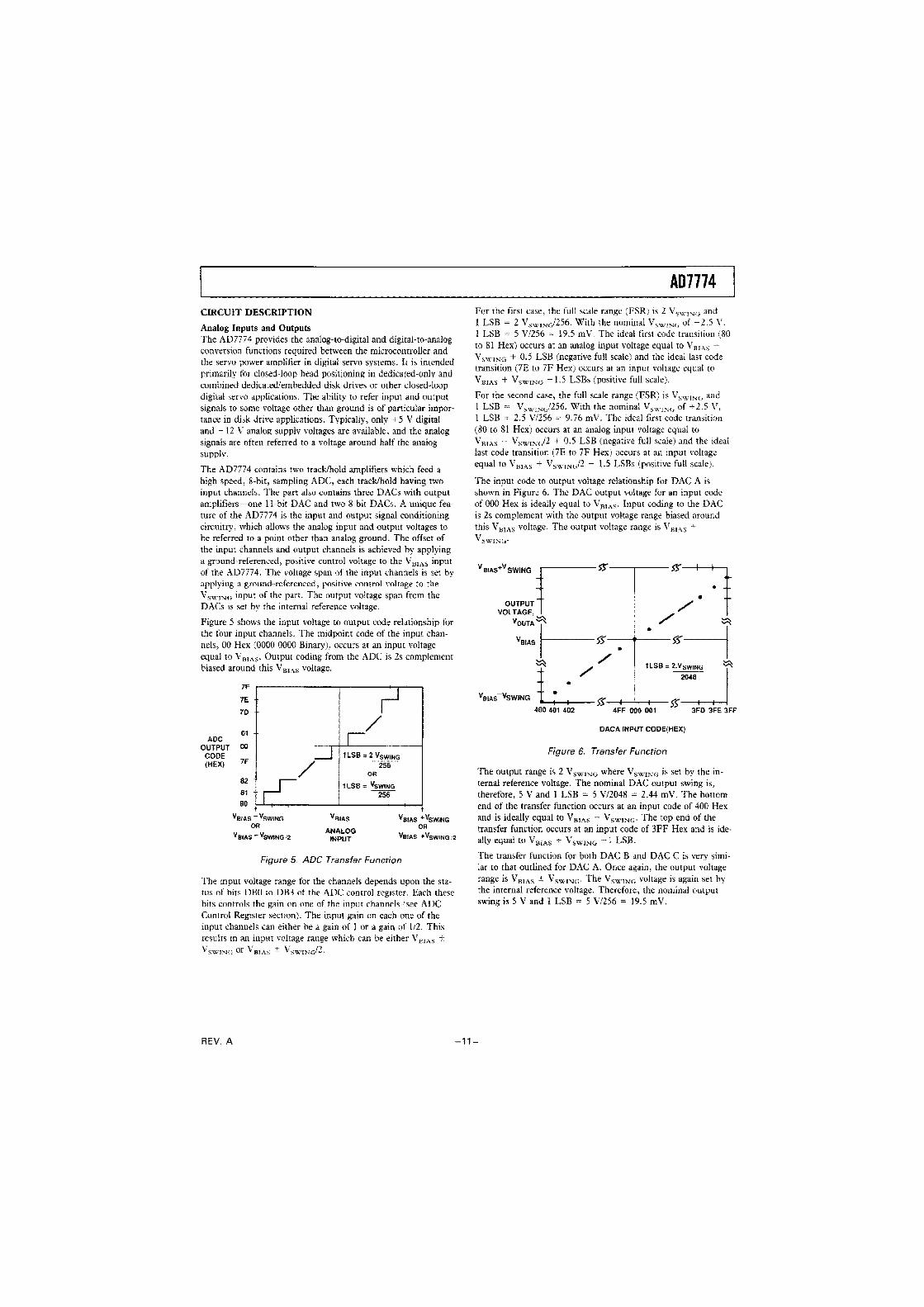
The input code to output voltage relationship for DAC A is shown in Figure 6. The DAC output voltage for an input codc of 000 Hex is ideally equal to VB1AS. Input coding to the DAC is 2s complement with the output voltage range biased around this VB[AS voltage. The output voltage range is VB,AS ± Vtmjwn.
VBIAS*V SWING
OUTPUT VOLTAGE,
- s r -
VOUTA '
VBIAS
"BIAS 'SWING
/
s r -
/
H 1- - t f -
-5T-
/
S3T
1 LSB = 2. V SWING 2048
- + - s r -400 401 402 4FF 000 001 " 3FD 3FE 3FF
DACA INPUT CODE(HEX)
Figure 6. Transfer Function
S i s 2 VS W I N G where VS W ] N G is ternal reference voltage. The nominal DAC output swing is, therefore, 5 V and 1 LSB = 5 V/2048 = 2.44 mV. The bottom end of the transfer function occurs at an input code of 400 Hex and is ideally equal to VB Ve The top end of the transfer function occurs at an input code of 3FF Hex and is ide-ally equal to VB i A S + V S W I N G - 1 LSB.
The transfer function for both DAC B and DAC C is very simi-lar to that outlined for DAC A. Once again, the output voltage range is VBIAS ± VS W I N G . The V s w i K G voltage is again set by the internal reference voltage. Therefore, the nominal output swing is 5 V and 1 LSB = 5 V/256 = 19.5 mV.
REV. A - 1 1 -

AD7774 The DAC output voltage for an input code of 00 Hex is ideally equal to V8 ! A S . input coding to the DACs is 2s complement with the output voltage range biased around this VBIAS voltage. The bottom end of the transfer function (negative full scale) oc-curs at an input code of 80 Hex and is ideally equal to VB1AS -VS W I N G . The top end of the transfer function (positive full scale) occurs at an input code of 7F Hex and is ideally equal to VHIAS
4 VS W I N G - I LSB. The input code to output voltage relationship for both DAC B and DAC C is shown in Figure 7.
BIAS+V SWING
OUTPUT VOLTAGE, yv
V OUTA
-sr-
VBIAS
/
- i— •53T—h
- j s t -
/ /
sr-
1LS8=2.VswiNG 256
H- -5T- H 1-80 81 82 FF 00 01 70 7E 7F
DACB/ DACC INPUT CODE (HEX)
Figure 7. DAC B/DAC C Transfer Function
Bias Voltage Conversions The voltage applied to the VBIAS pin of the AD7774 is applied internally to both track/holds. Each track/hold introduces some bias offset error on this input VBtAS voltage, and these errors may differ slightly from each other (typically less than 2 LSBs). The AD7774 provides the option to convert the bias voltage to estimate the bias offset error. Since both track/holds introduce different errors, the AD7774 allows the user to perform a con-version on the bias voltage at each track/hold. If this is done during a calibration routine, the bias offset error in each channel can be stored and compensated for in software. After a bias off-set conversion for Track/Hold A, the results are stored in ADC Latch A and for a bias offset conversion for Track/Hold B, the results are stored in ADC Latch B.
Driving the Analog Inputs and Reference Inputs The analog inputs, VA ] , VA2, VB1 and VB2 require up to I mA of input current and as such must be driven from low output impedance sources. In addition, the VB!AS and VS W J N G inputs must also be driven from low impedance sources. The VS W I N G
pin provides the internally generated swing voltage, but this can be overdriven by an externally applied voltage. This externally applied voltage will generate the VS W I N G voltage for the ADC but the for the DACs is always generated from the in-ternal swing voltage.
MICROPROCESSOR/MICROCOMPUTER INTERFACING The AD7774 is designed for easy interfacing to microprocessors and microcomputers as a memory mapped peripheral or an I/O device. In addition, the AD7774 high speed bus timing allows direct interfacing to most microprocessors including the DSP processors.
AD7774-ADSP-2101/ADSP-2105 Interface Figure 8 shows a typical interface to the DSP microcomputer, the ADSP-2101/ADSP-2I05. The ADSP-2I01/ADSP-2IG5 is optimized for high speed numeric processing tasks.
Because the instruction cycle of the ADSP-2101/ADSP-2105 is very fast, the WR and RD puises must be stretched out to suit the AD7774. This is easily achieved as the ADSP-2101/ADSP-2105 memory interface supports slower memories and memory-mapped peripherals with a programmable wait state generation capability. A number of wait states, from 0 to 7, can be speci-fied for each memory interface. One wait state is sufficient for the interface to the AD7774.
Conversion is initiated on the required ADC channel using a <DM(CST) = MR0> where CST is the relevant channel address. Writing data to the relevant AD7774 DAC or to the AD7774 ADC control register consists of a <DM(DAC) = MR0> instruction where DAC is the relevant DAC address or the address of the ADC control register. Two write opera-tions arc required to load the i l bits of data to DAC A. A con version result is read using the instruction <MR0 = DM(ADC)> where ADC is the address of the relevant ADC Latch.
' ADDITIONAL PINS OMITTED FOR CLARITY
Figure 8. AD7774 to ADSP-2101/ADSP-2105 interface
AD7774-TMS32GC10/TMS320C14 Interface A typical interface to the TMS320C10/TMS320C14 is shown in Figure 9. The AD7774 is mapped at a port address, and the interface is designed for the maximum TMS320C10 clock fre-quency of 20 MHz and the maximum clock frequency of 25 MHz for the TMS320C14.
Conversion is initiated on the selected AD7774 ADC channel using a single I/O instruction, <OUT CST,A> where CST is the relevant address for the selected channel. Writing data to the relevant AD7774 DAC or to the AD7774 ADC control register consists of an <OUT DAC,A> instruction where DAC is the relevant DAC address or the address of the ADC control regis-
- 1 2 - REV. A

AD7774 ter. Two write operations are required to load the 11 bits of data to DAC A. A conversion result is read using the instruction <IN A,ADC> where ADC is the address of the relevant ADC Latch.
* ADDITIONAL PINS OMITTED FOR CLARITY
Figure 9. AD7774 to TMS320CW/TMS320C14 interface
AD7774-TMS320C25 Interface Figure 10 shows an interface between the TMS320C25 and the AD7774. The TMS320C25 does not have separate RD and WR signals to drive the AD7774 RD and WR inputs directly. These have to be generated from the processor STRB and R/W out-puts with the addition of some logic gates.
Figure 10. AD7774 to TMS320C2S Interface
Once again, because the processor cycle time is so fast a wait state has to be inserted during read and write cycies to the AD7774. This is achieved by OR-gating the IS signal with the MSC signal to drive the READY input and, thereby, generate one wait state during every read and write operation to the AD7774.
Conversion is initiated on the selected AD7774 ADC channel using a single I/O instruction, <OUT CST,A> where CST is the relevant address for the selected channel. Writing data to the relevant AD7774 DAC or to the AD7774 ADC control register consists of an <OUT DAC,A> instruction where DAC is the relevant DAC address or the address of the ADC control regis-ter. Two write operations are required to load the 11 bits of data to DAC A. A conversion result is read using the instruction < IN A,ADC > where ADC is the address of the relevant ADC Latch.
AD7774-80C196 Interface Figure 11 shows a typical interface between the AD7774 and the 80C196 microcomputer. The microcomputer is configured in its 8-bit bus cycle mode and in the address valid strobe mode. In this mode, the high order 8 bits of the address bus appear on Port 4, while Port 3 contains the multiplexed data bus and lower order address bus.
Figure 11. AD7774 to 80C196 Interface
Conversion is initiated on the selected AD7774 ADC channel using a single I/O instruction, <STB CST,D> where CST is the relevant address for the selected channel and D is a location in the 80C196 register file or is immediate data. Writing data to the relevant AD7774 DAC or to the AD7774 ADC control regis-ter consists of an <STB DAC,D> instruction where DAC is the relevant DAC address or the address of the ADC control regis-ter and D is a location in the 80C196 register file or is immedi-ate data. Two write operations are required to load the 11 bits of data to DAC A. A conversion result is read using the instruc-tion <LDB D,ADC> where ADC is the address of the relevant ADC latch and D is a location in the 80C196 register file.
REV. A - 1 3 -

AD7774 AD7774-80C51 Interface A typical interface between the AD7774 and the 80C51 is shown in Figure 12. In this interface, Port 0 provides the multiplexed low order address and data bus, and Port 2 provides the high order address bus. The ALE signal from the 80C51 is used to demultiplex the address/data bus.
Conversion is initiated on the selected AD7774 ADC channel using a single instruction, <MOV CST,A> where CST is the relevant address for the selected channel and A is the 80C51 ac-cumulator. Writing data to the relevant AD7774 DAC or to the AD7774 ADC control register consists of an <MOV DAC,A> instruction where DAC is the relevant DAC address or the ad-dress of the ADC control register, and A is the 80C51 accumula-tor. Two write operations are required to load the 11 bits of data to DAC A. A conversion result is read using the instruction <MOV A,ADC> where ADC is the address of the relevant ADC Latch and A is the 80C51 accumulator.
Figure 12, AD7774 to 80C51 Interface
AD7774-68HC11 Interface Figure 13 shows an interface between the AD7774 and the 68HC11. In this interface, Port C provides the multiplexed low order address and data bus, and Port B provides the high order address bus. The AS signal from the 68HC11 is used to de-multiplex the address/data bus. The 68HCI1 does not have sep-arate RD and WR signals to drive the AD7774 RD and WR inputs directly. These have to be generated from the processor £ and R/W outputs with the addition of some logic gates. Conversion is initiated on the selected AD7774 ADC channel using a single instruction, <STAA CST> where CST is the relevant address for the selected channel. Writing data to the relevant AD7774 DAC or to the AD7774 ADC control register consists of an <STAA DAC> instruction where DAC is the relevant DAC address or the address of the ADC control regis-ter, and the data is loaded to the relevant register from the 68HC1I accumulator. Two write operations are required to load the 11 bits of data to DAC A. A conversion result is read using the instruction <LDAA ADC> where ADC is the address of the relevant ADC latch, and the conversion result is loaded to the 68HC11 accumulator.
PB.7
PB.O
6BHC11*
E R/W
AS
PC.7
PC.Q
Figure 13. AD7774 to 68HC11 Interface
APPLICATIONS The AD7774 servo I/O port is used to convert servo-related sig-nals between the analog and digital domains. The input struc-ture of the ADC makes it very easy to convert the typical output signals provided by a servo demodulator. In a magnetic disk drive employing a dedicated servo surfacc or a combined embedded/dedicated servo surface, the servo demod-ulator produces two, positive-only, quadrature signals, generally sinusoidal or triangular, from the di-bit patterns read from the servo surface. The quadrature signals have the form of V!JI V , -V S W I N G - T H E simultaneous sampling of the AD7774 input chan-nels allows conversion of these quadrature signals without intro-ducing significant phase delay errors. These converted signals provide the servo microcontroller with position and track cross-ing information from which velocity information can be derived. In optical disk drives, analogous servo signals can be derived from the quad photodiode detector to provide position and focus information for the microcontroller.
In dedicated servo drives and combined embedded/dedicated servo drives, the servo demodulator converts the servo informa-tion bit patterns from the disk into the standard N and Q {normal and quadrature) servo signals. The relative phase rela-tionship between these signals is important so the simultaneous sampling feature of the AD7774 is used to maintain the relative phase between the N and Q signals. The four channels of the AD7774 can be used to process information from two demodula-tors. Alternatively, two channels can be used for the N and Q signals with the other ADC channels used for current measure-ment, temperature measurement, calibration routines or other housekeeping functions.
In magnetic disk drives, a single voice coil motor is used to po-sition the head assembly and one DAC is usually sufficient to drive the motor in both the seek and track modes. In the seek mode the DAC can be used to generate directly the desired ana-log velocity trajectory which the head must travel in order to achieve minimum access times. Alternatively the DAC can gen-erate a servo error value (computed by the microcontroller) be-tween the actual head velocity and the desired head velocity. In
- 1 4 - REV. A

the track mode, the DAC can be used to provide a position er-ror signal to keep the head over the track or to dctect the head off-track, for such purposes as thermal compensation and soft-error retries. The DACs provide positive-only output signals of the form VBJAS ± V s w i h i G , which are ideal for driving voice coil motors. In general, up to 11 bits of resolution are required for a DAC to control the motor in both the seek and track modes. As a result, DAC A would generally be used to drive the voice coil motor. The other DAC channels can be used for programmable control of the loop filter or for AGC or programmable gain control.
A typical servo control loop using the AD7774 is shown in Fig-ure 14. In this dedicated servo example, the servo demodulator outputs (the N and Q signals) arc applied to the VA, and VB1
inputs of the AD7774. The voice coil motor current, I ( , is bidi-rectional and is supplied by the power transconductance ampli-fier. One input to this amplifier is held at VB[AS while the other input is driven from the DAC A output, V o t r x A . Typical input voltages for this power stage are shown in Figure 15. The transconductance, G r„ of the power stage is determined uy external sense resistors.
DRIVE INTERFACE
n MICROCONTROLLER
SERVO DEMODULATOR
SERVO SERVO HEAD PREAMP
SWING AD7774
VOICE ^ * B I A S
COIL MOTOR POWER
TRANSCONDUCTANCE AMPLIFIER
Figure 14. Typical Dedicated Servo Control Loop Using the AD7774
DAC in OUTPUT,
V
lL(MAX)= ± v s w ) f 4 G .G o
(l = VouTA'Gt,
Figure 15. Typical Relationship Between Input Voltage and Output Current for Transconductance Amplifier
Multichannel Expansion The AD7774 with its four input channels has the capability of monitoring the N and Q signals from two servo demodulators. With the addition of a multiplexer and a dual op amp, the sys-tem can be expanded so that the AD7774 handles the outputs from a number of servo demodulators. Using a differential mul-tiplexer as shown in Figure 16, the N and Q signals for each servo demodulator can still be simultaneously sampled. The ADG527A multiplexer is ideally suited since it is specified for single supply operation (12 V ± 10%).
The CS and WR inputs to the AD7774 are gated to provide the WR input to the ADG527A. The multiplexer input is selected on the falling edge of WR while the signal is latched on the ris-ing edge. The AD7774 starts conversion also on the rising edge of WR. Therefore, the output signal of the multiplexer must have settled to within 8 bits over the duration of the WR puise. The tO N (WR) and settling time of the ADG527A determine the width of the WR pulse.
N1 - S1A A2 A1 AO
N 2 - S2A N 3 -N 4 -
S3A S4A DA
N 8 - SSA
ADG527A*
Q 1 - S1B DB
0 2 - S2B
Q 3 - S3B
04 — S4B
G 8 - S8B WR
1 ADDITIONAL PINS OMITTED FOR CLARITY
Figure 16. Multichannel System
REV. A -15-

AD7774 MECHANICAL INFORMATION
OUTLINE DIMENSIONS Dimensions shown in inches and (mm).
28-Pin Plastic DIP (N-28)
A A A A A A A A A A A A A A ,
0.555 113.971 0.536 (13.4621
0.1 ? S 14 461 0.06511.65] 0.020 IS 5GS) 0 12013 (!$) 0.046(1.141 0.015(0.381) 0 095 1
LEAD N O 1 IDENTIFIED BY DOT OR NOTCH L E A D S A R £ SOLDER DIPPED OR TIN.PLATED ALLOY a ? OH COPPER
28-Pin PLCC (P-28A)
i n n n n n n N O . L P I N
I D E N T I F I E R
TOP VIEW
' U D " U U U U U 0.456 111.SMI , 0
0 *50 (11.4301
«iS®ilM2<:ri 0 485(12 3 2 ) "
/ i n > 3 1 : :
<c Oi
z a UJ H z E CL
-16 - REV. A