
Comparative study of asymmetric versus symmetric planar slab dielectric optical waveguides
Upload
independentCategory
view
1download
0
149J Opt 38 (3) : 149–159
13
J Opt 38 (3) : 149–159
RESEARCH ARTICLE
Fabrication and performance-analysis of a planar silica-based cascaded
symmetric Y-branch 1 8 optical power splitter
Suchandan Pal · Ashok Chauhan · Pawan Kumar · Mahendra Singh · Sona Das · Mukesh Sharma ·
Nirmal Pradhan · Kuldip Singh · Subodh Johri · C Dhanavantri · Anuj Bhatnagar · Babu Ram Singh
Received: 18 April 2009 / Accepted: 13 July 2009
© Optical Society of India 2009
S. Pal (�) · A. Chauhan · P. Kumar · M. Singh · S. Das · M. Sharma · N. Pradhan · K. Singh · S. Johri · C Dhanavantri· A. Bhatnagar* · B. R. Singh**Opto-electronic Devices Group, Central Electronics Engineering Research Institute (Council of Scientific andIndustrial Research), Pilani - 333 031, Rajasthan, India.* Optoelectronics Division, SAMEER, Mumbai, India.** Previously at: CEERI, Pilani; Presently at: IIIT, Allahabad, India.
E-mail: [email protected]
Abstract Fabrication of a planar silica-based cascaded symmetric Y-branch 1 8 optical power splitter is described
in this study. Post-fabrication, thorough analysis of device-performance is presented in terms of insertion loss, non-
uniformity and polarization-dependent loss. The fabricated device is designed based on cascaded Y-branching waveguide,
comprising of a linear taper and symmetric S-bend arc branching waveguides. The simulated values of the average
insertion loss, non-uniformity and polarization-dependent loss at the wavelength of 1550 nm are found to be 9.37 dB,
0.35 dB and 0.04 dB respectively. However, the above parameters have been measured to be around 17.5 dB, 1.5 dB
and 1.8 dB respectively, for the fabricated device at that wavelength. Measured parameters are compared with the
simulated results over a wavelength region of C & L band range. Some preventive points to minimize the deviation of
the measured values of the parameters from those of the simulated results are also discussed.
Key words Planar lightwave · Integrated-optic components · Optical splitter · Y-branch waveguide · Insertion loss
· Non-uniformity polarization-dependent loss · Photo-lithography · Plasma-enhanced chemical vapour deposition ·Reactive-ion etching.
Introduction
Compact and low-cost planar integrated optical components [1] play major roles for the deployment of optical
technologies to meet the ever-increasing demand of broadband WDM communication system including the passive

150 J Opt 38 (3) : 149–159
13
optical networks for fibre-to-the-home (FTTH) applications. Passive optical networks require optical splitters/
combiners in order to split/combine the optical powers in the subscriber networks. 1 N optical splitter divides the
optical signal into N number of branches. In order to realized a compact and cost-effective optical splitter, various
groups of researchers have designed, fabricated and demonstrated different technologies like Y-branch splitter [1-6],
multi-mode interference based splitter [7], directly UV-written optical splitter [8] and so on. Among these, Y-branch
optical splitter is much popular because of its design simplicity.
On the other side, silica-based planar lightwave circuits (PLCs) and technology have found a considerable
attention for the development of various commercially viable photonic components. This is mainly because of the
intrinsic advantage of highly matured processing technology leading to a significant reduction in fabrication expenses
of the components. In addition to that, silica has the inherent properties like low insertion loss leading to an excellent
compatibility to the optical fibres for device coupling, possibility of hybrid integration and long-term reliability.
Further, the availability of large size wafers with high purity and excellent mechanical and thermal properties of
silicon material makes it very suitable and the most promising candidate for the integration platform or the optical
bench.
Therefore, a planar silica-based Y-branch 1 8 optical splitter is attempted for realization and for its characterization.
However, the most crucial regions of the Y-branch 1 8 optical splitter are the branching points of the splitting
junctions at three different sections of the device, such as, at 1 2, 2 4 and 4 8 branching points. Various geometries
of Y-branch have been proposed to minimize the branching losses [5,6,9,10]. In this paper, the fabrication and
thorough characterization of a planar silica-based cascaded symmetric Y-branch optical power splitter is presented,
the design of which is optimized with Y-branching waveguide comprising of a linear taper and symmetric S-bend arc
branching waveguides. A linear taper has been incorporated in order to reduce the tilt effect on the modal tails thereby
resulting in the lower excess loss in the splitting junction.
Design and fabrication
Figure 1 describes a schematic diagram of a 1 2 optical power splitter based on silica-on-silicon material, which
consists of three sections – straight waveguide, linear taper and S-bend arc waveguide. A sufficiently thick undoped
silica buffer layer on top of the silicon substrate has been considered in order to avoid the substrate radiation. A Ge-
doped
silica and a boro-phospho-silicate-glass (BPSG)-based silica on top of the guiding layer, have been considered as
the guiding and over-cladding layers respectively. The over-cladding with such a material is considered for matching
its refractive index with that of the under-cladding silica buffer layer.
Fig. 1 A schematic diagram of a section of a silica-based Y-branch 1 8 optical power splitter

151J Opt 38 (3) : 149–159
13
The proposed 1 8 optical power splitter has been designed by cascading this 1 2 splitter symmetrically by
using a 2D beam propagation method (BPM) software tool (based on the unconditionally stable finite difference
method algorithm of Crank and Nicolson), where the refractive indices (RI) of the guiding and the cladding (both
under- and over-cladding) materials have been considered as 1.450 and 1.444 (with a refractive index contrast,
0.3%) respectively at the wavelength of 1550 nm. The dimension of the channel waveguide has been optimized as 8
m (width, W) 8 m (height, T) in order to achieve a single mode propagation of operation along the length of the
waveguide at 1550 nm. All the eight output branches of the device are designed exactly 250 m apart from each other
(center-to-center), so that it can be coupled perfectly with commercially available V-grooved fibre array ribbons. The
overall dimension of the device has been achieved as around 21.5 mm (length) 1.76 mm (width). A similar
simulation result for this device with the variation of the optical field and the effective refractive index along the
propagation distance, as well as with the device width at an operational wavelength of 1550 nm, has already been
reported [2]. However, the performance of the designed and the fabricated 1 8 optical power splitter has been
analyzed in terms of the insertion loss, non-uniformity and the polarization-dependent loss (PDL) in this paper over
the conventional (C) and the long (L) wavelength region of the optical communication window.
Following design optimization, the device has been fabricated maintaining a number of sequential process steps,
for which each unit processes were initially optimized. A Ge-doped silica layer (RI: 1.4501 and Loss: 0.05 dB/cm at
1550 nm for TE-mode, measured by Metricon 2010 prism coupler) of 8 m thick deposited on top of 15 m
thermally oxided (RI: 1.4457 at 1550 nm for TE-mode, measured by Metricon 2010) 4” silicon wafer, supplied by M/
s KST, USA, has been taken as a starting material. Point to be noted that the measured loss of Ge-doped silica layer
is combined total of scattering loss (from particles and other scattering centers and surface roughness) and loss due to
the inherent absorption of the waveguide material. Such a thick thermal oxide buffer layer has been used in order to
prevent the light leakage to the substrate [11]. For ease in process handling, the wafer was diced into a number of
rectangular pieces according to the dimension of the device. The wafer-piece was spin-coated with a positive photo-
resist, S1818 (from Shipley, USA). After an appropriate pre-baking of the coated wafer, it was UV-exposed by using
MJB3 mask aligner with a dark-field mask (i.e., transparent device pattern in an opaque mask), where the UV-light
can pass only through the device pattern, making the positive photoresist soften in this region. So, after processing
with a compatible developer, an exact device pattern was generated on the wafer by removing the soften photoresist.
Subsequently, a thin layer (~ 180 nm) of nichrome-based metal pattern of the device was achieved after carrying out
a series of process steps like proper post-baking, ashing, e-beam evaporation-based metalization and lift-off. E-beam
evaporation causes the deposition of thin metal layer with poor step-coverage at relatively low temperature on top
of the patterned wafer (coated with ~ 1.8 micron thick S1818-based resist, except the device pattern), making the lift-
off process much efficient. This metal pattern is required for masking of the device in real material, i.e., to achieve the
8 m deep ridge waveguide based splitter pattern in Ge-doped silica layer by dry etching through ECR-RIE
technique. In an optimized condition of this dry etching process, by use of an indigenously developed ECR-RIE
equipment, CHF3 and Ar gases were applied at flow-rate of 16 sccm and 8 sccm respectively at a chamber pressure
of 50 mTorr with a RF power of ~ 200 W, where an average etch-rate of ~ 1500 Aº/min was achieved. Upon realization
of 8 m deep ridge pattern, the nichrome layer was removed by using a liquid nichrome etchant. At this point, it is
worthwhile to mention that the above process of lift-off could be avoided by fabricating the device with the help of
bright-field mask. However, following photo-lithography on the metaldeposited silica-on-silicon sample-wafer,
there would be a possibility of non-uniformity in etching (under- or overetching) during the wet process of metal
etching, which makes the width of the metal pattern of the device nonuniform, resulting in worse side-wall roughness
during deep dry etching to realize the waveguide.

152 J Opt 38 (3) : 149–159
13
A BPSG-based silica layer was deposited on top of the ridge waveguide pattern by PECVD technique using the
equipment supplied by STS, UK, in order to achieve the proposed channel waveguide based optical splitter.
Appropriate B and P-doping levels has been chosen by adjusting the flow of diborane (B2H6) and phosphine (PH3)
in order to match the refractive-index of the over-cladding to that of the thermal oxide under-cladding layer, and to
optimize the reflow properties of the glass over the waveguide. The values of refractive index and thickness of this
layer were found to be 1.4445 (at 1550 nm) and ~ 12 m, measured by Metricon 2010. Such a thick BPSG layer was
deposited in two steps; each step consists of deposition of around 6 m thickness, followed by a process of
annealing at a temperature of 1000°C for ~ four hours, before going into the step of further 6 m deposition and
annealing. This is to minimize the two large absorption peaks in the 1.4 – 1.6 m wavelength region associated with
simultaneous both Si – H (third harmonic) and N – H (second harmonic) bonds and with the well-known O – H bonds,
which cause larger absorption at 1.506 m and relatively smaller absorption at 1.4 m respectively. Both absorption
peaks can be successfully removed the process of thermal annealing [12] as mentioned above.
Figures 2(a), 2(b) and 2(c) represent the micrograph of the three different portions of the fabricated device, such
as, 1 2, 2 4 and 4 8 branching sections of the 1 8 optical splitter. The device was then diced precisely with a dicing
machine (Model: DISCO, DAD321, Japan) according to the exact device length. Input/output facets of the device
were polished in a polishing machine (Model: Allied TechPrep, Allied High Tech Products Inc., USA) by fixing it to
an appropriate zig and using various polishing sheets with different grain size from 30micron to 0.1 micron in a
sequential step, and finally with a silica-gel based colloidal solution in order to achieve mirror-like input/output edges
for measurement of the device with minimum coupling loss.
Fig. 2 Various sections of 1×8 optical power splitter after fabrication, (a) 1×2 branch section, (b) 2×4 branch
section, and (c) 4×8 branch section
(a) (b) (c)
Measurement results and discussion
Initially, a manual fibre alignment system (Newport, USA) having twin precision alignment stages was used for the
characterization of the device. A He-Ne laser (JDS 1135) with 10 mW output power was used for the visible
alignment. A 1-channel FC/PC connectorised V-grooved fibre-array (FA) ribbon was used along with 5 – 10
microscope objective for launching the visible light into the input of the device, and the output of the device was
observed with a similar 5 – 10 microscope objective. After an appropriate alignment with the visible light, the
splitter was tested to observe the output spots at 1550 nm, with the help of a Agilent 81640A tunable laser. Fig. 3(a)
shows the eight distinct output spots captured by a CCD camera, when the splitter was tested at this wavelength.
After preliminary analysis by viewing the captured photograph of the near-field pattern of every single output spot
[a photograph of one of the best spots is shown in Fig. 3(b)], it was found to be a single-mode. Finally, the 1 8 optical

153J Opt 38 (3) : 149–159
13
splitter was pig-tailed and subsequently packaged by a Photonics Packaging Automation System (Newport, USA).
A 1-channel and a 8-channel (center-to-center channel separation: 250 m) FC/PC connectorised V-grooved fibre-
array (FA) ribbon were used at the input and output of the device respectively. After an appropriate alignment, FC/
PC connectorised V-grooved FA ribbons were attached to the device input and output with a UV-curable NOA-61
epoxy. Fig. 4 displays a photograph of the pig-tailed 1 8 optical power splitter after fixing it within a proper
packaging case.
Fig. 3 Photograph of (a) eight distinct spots at the output of the 1×8 optical splitter, when tested at 1550 nm
with the help of an Agilent 81640A tunable laser source along with (b) a near-field pattern of one of the best
single output spots at this wavelength
Fig. 4 Photograph of a packaged 1×8 optical splitter. Input and output of the device have been attached to 1-
channel and 8-channel FC/PC connectorised V-grooved fibre array ribbons respectively
154 J Opt 38 (3) : 149–159
13
In the next stage, the performance of the fabricated 1 8 optical splitter has been analyzed in terms of total
insertion loss, power non-uniformity and PDL. The total insertion loss is defined by the ratio of the output to the
input power, which includes the propagation loss as well as the loss induced by mode conversion and coupling. The
power nonuniformity has been defined as the ratio of the individual output power at any port to the average output
power. In a similar way, the PDL has been defined as the ratio of the output power corresponding to TE- and TM-
polarized light, for any port. Measured values of the above parameters have also been compared with those obtained
from the simulation. The simulated values of the average insertion loss, non-uniformity and PDL at the wavelength
of 1550 nm have been found to be 9.37 dB, 0.35 dB and 0.04 dB respectively. However, the above parameters have
been observed to be around 17.5 dB, 1.5 dB and 1.8 dB respectively, when measured with the fabricated device at that
wavelength. At this point, it is worth mentioning that the measured values of insertion loss include the propagation
loss, excess loss and the coupling losses at the input and output of the device.
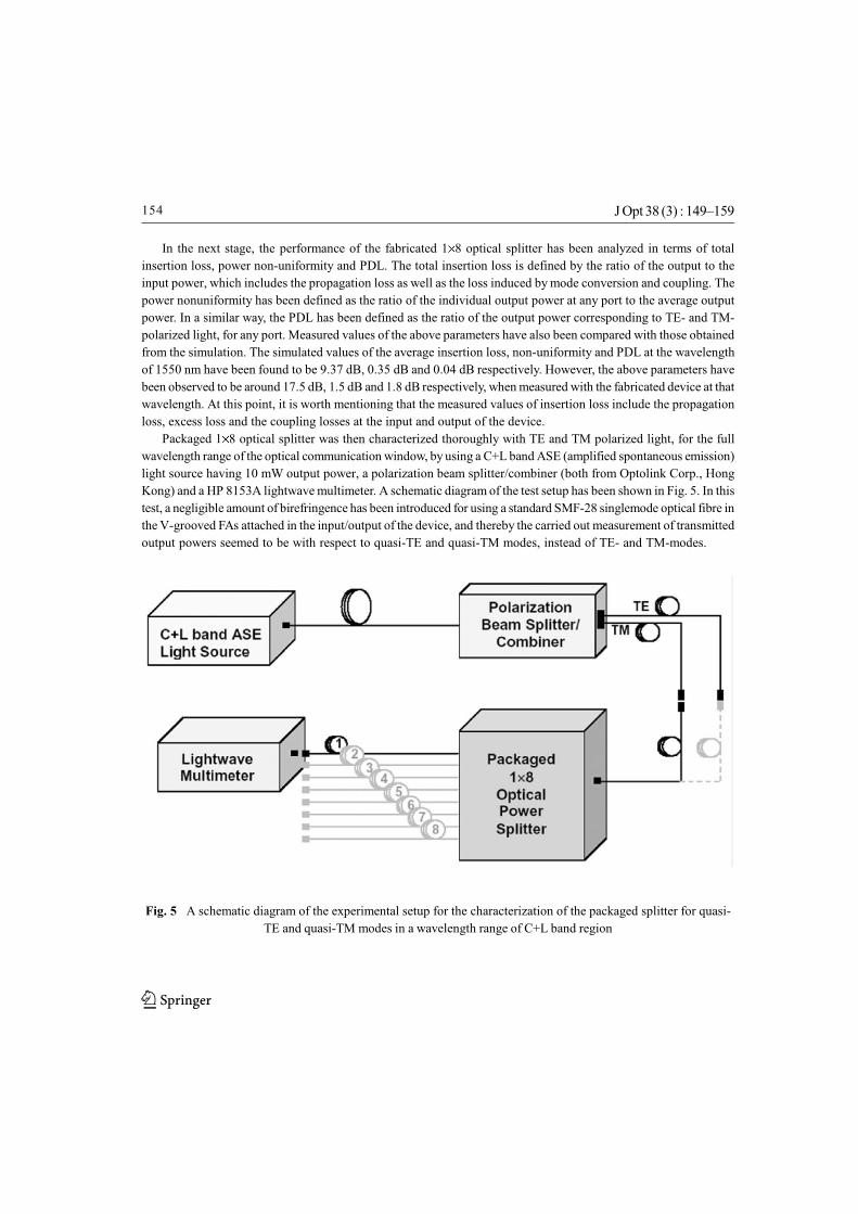
Packaged 1 8 optical splitter was then characterized thoroughly with TE and TM polarized light, for the full
wavelength range of the optical communication window, by using a C+L band ASE (amplified spontaneous emission)
light source having 10 mW output power, a polarization beam splitter/combiner (both from Optolink Corp., Hong
Kong) and a HP 8153A lightwave multimeter. A schematic diagram of the test setup has been shown in Fig. 5. In this
test, a negligible amount of birefringence has been introduced for using a standard SMF-28 singlemode optical fibre in
the V-grooved FAs attached in the input/output of the device, and thereby the carried out measurement of transmitted
output powers seemed to be with respect to quasi-TE and quasi-TM modes, instead of TE- and TM-modes.
Fig. 5 A schematic diagram of the experimental setup for the characterization of the packaged splitter for quasi-
TE and quasi-TM modes in a wavelength range of C+L band region
155J Opt 38 (3) : 149–159
13
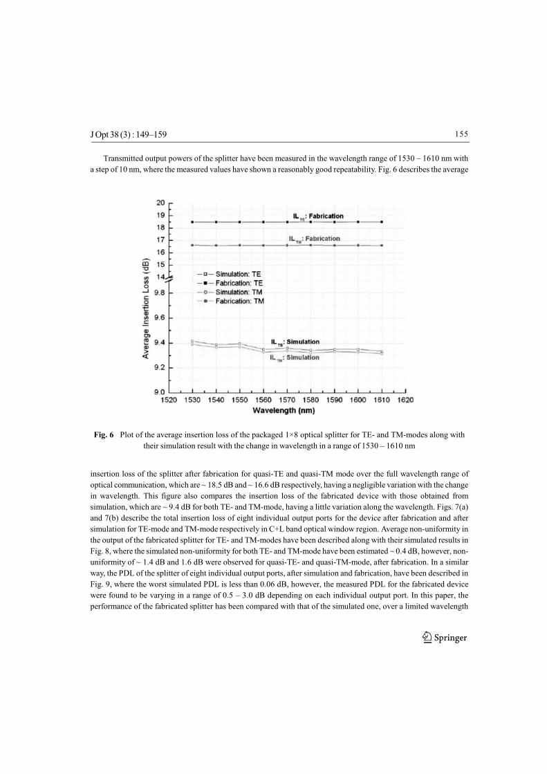
Transmitted output powers of the splitter have been measured in the wavelength range of 1530 – 1610 nm with
a step of 10 nm, where the measured values have shown a reasonably good repeatability. Fig. 6 describes the average
Fig. 6 Plot of the average insertion loss of the packaged 1×8 optical splitter for TE- and TM-modes along with
their simulation result with the change in wavelength in a range of 1530 – 1610 nm
insertion loss of the splitter after fabrication for quasi-TE and quasi-TM mode over the full wavelength range of
optical communication, which are ~ 18.5 dB and ~ 16.6 dB respectively, having a negligible variation with the change
in wavelength. This figure also compares the insertion loss of the fabricated device with those obtained from
simulation, which are ~ 9.4 dB for both TE- and TM-mode, having a little variation along the wavelength. Figs. 7(a)
and 7(b) describe the total insertion loss of eight individual output ports for the device after fabrication and after
simulation for TE-mode and TM-mode respectively in C+L band optical window region. Average non-uniformity in
the output of the fabricated splitter for TE- and TM-modes have been described along with their simulated results in
Fig. 8, where the simulated non-uniformity for both TE- and TM-mode have been estimated ~ 0.4 dB, however, non-
uniformity of ~ 1.4 dB and 1.6 dB were observed for quasi-TE- and quasi-TM-mode, after fabrication. In a similar
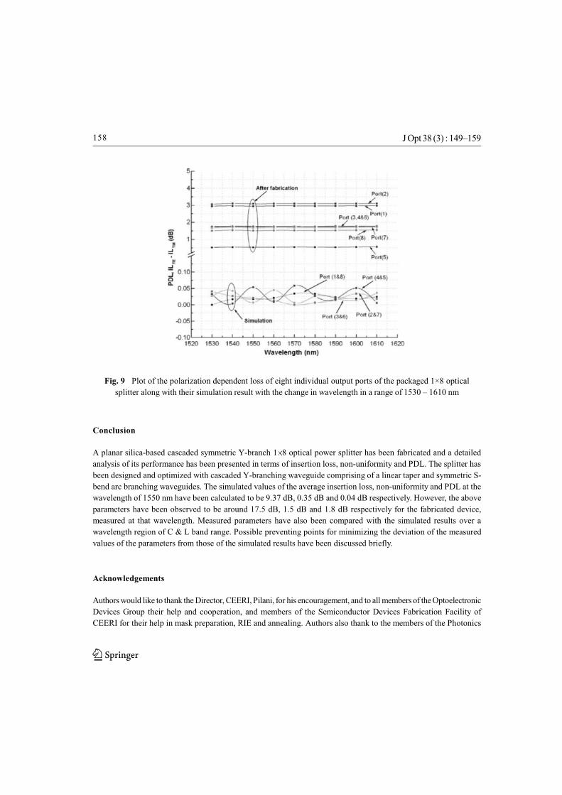
way, the PDL of the splitter of eight individual output ports, after simulation and fabrication, have been described in
Fig. 9, where the worst simulated PDL is less than 0.06 dB, however, the measured PDL for the fabricated device
were found to be varying in a range of 0.5 – 3.0 dB depending on each individual output port. In this paper, the
performance of the fabricated splitter has been compared with that of the simulated one, over a limited wavelength

156 J Opt 38 (3) : 149–159
13
Fig. 7 (a) Plot of insertion loss for eight individual output ports of the packaged 1×8 optical splitter for TE-
mode along with their simulation result with the change in wavelength in a range of 1530 – 1610 nm
range of 1530 – 1610 nm with the help of an ASE light source, due to unavailability of a highpower extended
broadband light source. However, the simulated performance of the device was found to be similar (a flat response)
when the operational wavelength was decreased up to ~1300 nm in the lower wavelength side. A similar flat response
of the fabricated device is also expected over this extended wavelength region making the splitter suitable for FTTH
applications, where the device should operate either or all three wavelengths of 1310 nm (for voice and data up-
stream), 1490 nm (for voice and data down-stream) and 1550 nm (for video down-stream). However, in this case the
connecting optical fibre (low water peak type, ITU G562 C/D) would be different from the standard communication
fibre.
In all the above figures, a significant amount of deviation has been found in the measured values of the parameters
from those of simulation. This margin between the simulation and the fabrication results can be minimized by (a)
reducing the surface and side-wall roughness of the waveguides after optimization of all critical processes like
lithography, lift-off and RIE, (b) considering a technology-compatible design after introducing a finite gap of ~ 2 m
at each individual splitting junctions, which can overcome the limitation in fabrication process steps during RIE and
PECVD after removing voids at junction points (c) optimizing taper angles and taper shapes in each individual
sections and so on. In addition, input and output facets of the device play vital role in order to achieve minimum
coupling losses, which is much essential before pig-tailing the device. Further, the measured insertion loss of the
fabricated splitter includes this coupling loss in our measurement, and therefore the actual insertion loss can be
estimated by deducting the input/output coupling losses. This can be done after fabricating a straight waveguide
within the same substrate. A technology compatible design of the same device has been made by considering the
above points and its performance would be reported soon.

157J Opt 38 (3) : 149–159
13
Fig. 7 (b) Plot of insertion loss for eight individual output ports of the packaged 1×8 optical splitter for TM-
mode along with their simulation result with the change in wavelength in a range of 1530 – 1610 nm
Fig. 8 Plot of the average non-uniformity of the packaged 1×8 optical splitter for TE- and TM-modes along with
their simulation result with the change in wavelength in a range of 1530 – 1610 nm
158 J Opt 38 (3) : 149–159
13
Fig. 9 Plot of the polarization dependent loss of eight individual output ports of the packaged 1×8 optical
splitter along with their simulation result with the change in wavelength in a range of 1530 – 1610 nm
Conclusion
A planar silica-based cascaded symmetric Y-branch 1 8 optical power splitter has been fabricated and a detailed
analysis of its performance has been presented in terms of insertion loss, non-uniformity and PDL. The splitter has
been designed and optimized with cascaded Y-branching waveguide comprising of a linear taper and symmetric S-
bend arc branching waveguides. The simulated values of the average insertion loss, non-uniformity and PDL at the
wavelength of 1550 nm have been calculated to be 9.37 dB, 0.35 dB and 0.04 dB respectively. However, the above
parameters have been observed to be around 17.5 dB, 1.5 dB and 1.8 dB respectively for the fabricated device,
measured at that wavelength. Measured parameters have also been compared with the simulated results over a
wavelength region of C & L band range. Possible preventing points for minimizing the deviation of the measured
values of the parameters from those of the simulated results have been discussed briefly.
Acknowledgements
Authors would like to thank the Director, CEERI, Pilani, for his encouragement, and to all members of the Optoelectronic
Devices Group their help and cooperation, and members of the Semiconductor Devices Fabrication Facility of
CEERI for their help in mask preparation, RIE and annealing. Authors also thank to the members of the Photonics

159J Opt 38 (3) : 149–159
13
Division of IRDE, Dehradun for edge-polishing of the sample-devices and the members of the Optoelectronics
Division of SAMEER, Mumbai for pig-tailing and packaging of the device with their existing facilities.
References
1. H. Nishihara, M. Haruna, and T. Suhara, Optical Integrated Circuits, In: RE.Fisher and Warren J.Smith (Eds.),
Optical and Electro-Optical Engineering Series, McGraw-Hill (1989)
2. A. Baby, C. Dhanvantri, J.P. Pachauri, S. Johri, P. Kumar and B.R. Singh, “Silica-on-Silicon based 1×N optical
splitter: Design, Fabrication and Characterization”, Indian J Eng Mater Sci, 12, 12–16 (2005)
3. C.G. Someda, Simple way to understand the behavior of an optical Y-junction, Electron Lett, 20, 349–350 (1984)
4. H. Yajima, Coupled Mode Analysis of Dielectric Planar Branching Waveguides, IEEE J Quantum Electron, QE-
14, 749–755 (1978)
5. J. Gamet and G. Pandraud, Ultra-Low Loss 1×8 Splitter Based on Field Matching Y-Junction, IEEE Photonics
Technol Lett, 16, 2060–2062 (2004)
6. J. Gamet and G. Pandraud, “Field matching Y-branch for low loss power splitter”, Opt Commun, 248, 423–429
(2005)
7. Q. Wang, S. He, and L. Wang, “A low-loss Y-branch with a multimode waveguide transition section”, IEEE
Photon Technol Lett, 14, 1124–1126 (2002)
8. M. Olivero and M. Svalgaard, “Fabrication of 2×8 power splitters in silica-on-silicon by the direct UV writing
technique”, IEEE Photon Technol Lett 18, 802–804 (2006)
9. S. Suzuki, T. Kitoh, Y. Inoue, Y. Yamada, Y. Hibino, K. Moriwaki, and M. Yanagisawa, Integrated optic Ybranching
waveguides with an asymmetric branching ratio, Electron Lett, 32, 735–736 (1996)
10. S.H. Tao, Q. Fang, J.F. Song, M.B. Yu, G.Q. Lo, and D.L. Kwong, “Cascade wide-angle Y-junction 1 16 optical
power splitter based on silicon wire waveguides on silicon-on-insulator”, Opt Express, 16, 21456–21461 (2008)
11. H. Ou, “Different index contrast silica-on-silicon waveguides by PECVD”, Electron Lett 39, 212–213 (2003)
12. G. Grand, J.P. Jadot, H. Denis, S. Valette, A. Fournier, and A.M. Grouillet, “Low-loss PECVD silica channel
waveguides for optical communications”, Electron Lett 26, 2135–2137 (1990)
Copyright © 2022 FDOKUMEN