Symmetric Graphene Dielectric Nanowaveguides as Ultra ...
12
nanomaterials Article Symmetric Graphene Dielectric Nanowaveguides as Ultra-Compact Photonic Structures Da Teng * ,† , Yuncheng Wang † , Tianzi Xu, Huayu Wang, Qinqin Shao and Yanan Tang * Citation: Teng, D.; Wang, Y.; Xu, T.; Wang, H.; Shao, Q.; Tang, Y. Symmetric Graphene Dielectric Nanowaveguides as Ultra-Compact Photonic Structures. Nanomaterials 2021, 11, 1281. https://doi.org/ 10.3390/nano11051281 Academic Editor: Detlef W. Bahnemann Received: 1 April 2021 Accepted: 10 May 2021 Published: 13 May 2021 Publisher’s Note: MDPI stays neutral with regard to jurisdictional claims in published maps and institutional affil- iations. Copyright: © 2021 by the authors. Licensee MDPI, Basel, Switzerland. This article is an open access article distributed under the terms and conditions of the Creative Commons Attribution (CC BY) license (https:// creativecommons.org/licenses/by/ 4.0/). College of Physics and Electronic Engineering, Zhengzhou Normal University, Zhengzhou 450044, China; [email protected] (Y.W); [email protected] (T.X); [email protected] (H.W.); [email protected] (Q.S) * Correspondence: [email protected] (D.T.); [email protected] (Y.T.) † These authors contributed equally to this work. Abstract: A symmetric graphene plasmon waveguide (SGPWG) is proposed here to achieve excellent subwavelength waveguiding performance of mid-infrared waves. The modal properties of the fundamental graphene plasmon mode are investigated by use of the finite element method. Due to the naturally rounded tips, the plasmon mode in SGPWG could achieve a normalized mode field area of ~10 -5 (or less) and a figure of merit over 400 by tuning the key geometric structure parameters and the chemical potential of graphene. In addition, results show that the modal performance of SGPWG seems to improve over its circular counterparts. Besides the modal properties, crosstalk analysis indicates that the proposed waveguide exhibits extremely low crosstalk, even at a separation distance of 64 nm. Due to these excellent characteristics, the proposed waveguide has promising applications in ultra-compact integrated photonic components and other intriguing nanoscale devices. Keywords: graphene plasmons; waveguides; subwavelength structures; mid-infrared waves 1. Introduction Plasmonic waveguides (PWGs) [1], which can confine and guide light at the subwave- length scale, are one of the components necessary to realize ultra-high-density photonic integration [2]. The traditional noble metallic PWGs, such as metal stripe/nanowire waveg- uides [3–5], channel/wedge plasmon waveguides [6], gap plasmon waveguides [7–9], dielectric-loaded plasmon waveguides [10–12], and hybrid PWGs [1,13–18], have been intensively studied in the near-infrared and visible bands. However, in the mid- and far-infrared bands, the plasmonic effects of metals (which were modeled as perfect electric conductors) are very weak and the electromagnetic optical response cannot be dynamically adjusted, which imposes restrictions on their applications at the nanoscale [19,20]. Thus, finding appropriate materials for PWGs is an urgent need. To address this critical challenge, researchers have suggested some available materials with tunable properties for exciting surface plasmons [21], including graphene [22–24], transition metal dichalcogenides [25–27], bulk Dirac semimetals [28,29], borophene [30,31], etc. Among these, graphene plasmons (GPs) have attracted widespread attention due to their advantages, including strong light–matter interactions, deep subwavelength field confinement, and tunable optical properties [23,24]. Benefiting from these excellent char- acteristics, graphene has served as an effective nanoscale waveguiding platform in the infrared region. More importantly, the combination of graphene and silicon-on-insulator (SOI) waveguides make it possible to design graphene-based photonic integration de- vices [32], such as waveguides [33–39], sensors [40,41], filters [42], modulators [43,44], etc. Recently, graphene–SiO 2 –Si coaxial-like waveguides [45], graphene layer–SiO 2 –Si planar structures [46–50], and graphene-coated nanowires integrated with SiO 2 or Si sub- strates [51–56] were presented to demonstrate ultra-compact photonic integrated circuits in the mid- and far-infrared bands. Nanomaterials 2021, 11, 1281. https://doi.org/10.3390/nano11051281 https://www.mdpi.com/journal/nanomaterials
-
Upload
khangminh22 -
Category
Documents
-
view
1 -
download
0
Transcript of Symmetric Graphene Dielectric Nanowaveguides as Ultra ...

nanomaterials
Article
Symmetric Graphene Dielectric Nanowaveguides asUltra-Compact Photonic Structures
Da Teng *,† , Yuncheng Wang †, Tianzi Xu, Huayu Wang, Qinqin Shao and Yanan Tang *
�����������������
Citation: Teng, D.; Wang, Y.; Xu, T.;
Wang, H.; Shao, Q.; Tang, Y.
Symmetric Graphene Dielectric
Nanowaveguides as Ultra-Compact
Photonic Structures. Nanomaterials
2021, 11, 1281. https://doi.org/
10.3390/nano11051281
Academic Editor: Detlef
W. Bahnemann
Received: 1 April 2021
Accepted: 10 May 2021
Published: 13 May 2021
Publisher’s Note: MDPI stays neutral
with regard to jurisdictional claims in
published maps and institutional affil-
iations.
Copyright: © 2021 by the authors.
Licensee MDPI, Basel, Switzerland.
This article is an open access article
distributed under the terms and
conditions of the Creative Commons
Attribution (CC BY) license (https://
creativecommons.org/licenses/by/
4.0/).
College of Physics and Electronic Engineering, Zhengzhou Normal University, Zhengzhou 450044, China;[email protected] (Y.W); [email protected] (T.X); [email protected] (H.W.);[email protected] (Q.S)* Correspondence: [email protected] (D.T.); [email protected] (Y.T.)† These authors contributed equally to this work.
Abstract: A symmetric graphene plasmon waveguide (SGPWG) is proposed here to achieve excellentsubwavelength waveguiding performance of mid-infrared waves. The modal properties of thefundamental graphene plasmon mode are investigated by use of the finite element method. Due tothe naturally rounded tips, the plasmon mode in SGPWG could achieve a normalized mode field areaof ~10−5 (or less) and a figure of merit over 400 by tuning the key geometric structure parameters andthe chemical potential of graphene. In addition, results show that the modal performance of SGPWGseems to improve over its circular counterparts. Besides the modal properties, crosstalk analysisindicates that the proposed waveguide exhibits extremely low crosstalk, even at a separation distanceof 64 nm. Due to these excellent characteristics, the proposed waveguide has promising applicationsin ultra-compact integrated photonic components and other intriguing nanoscale devices.
Keywords: graphene plasmons; waveguides; subwavelength structures; mid-infrared waves
1. Introduction
Plasmonic waveguides (PWGs) [1], which can confine and guide light at the subwave-length scale, are one of the components necessary to realize ultra-high-density photonicintegration [2]. The traditional noble metallic PWGs, such as metal stripe/nanowire waveg-uides [3–5], channel/wedge plasmon waveguides [6], gap plasmon waveguides [7–9],dielectric-loaded plasmon waveguides [10–12], and hybrid PWGs [1,13–18], have beenintensively studied in the near-infrared and visible bands. However, in the mid- andfar-infrared bands, the plasmonic effects of metals (which were modeled as perfect electricconductors) are very weak and the electromagnetic optical response cannot be dynamicallyadjusted, which imposes restrictions on their applications at the nanoscale [19,20]. Thus,finding appropriate materials for PWGs is an urgent need.
To address this critical challenge, researchers have suggested some available materialswith tunable properties for exciting surface plasmons [21], including graphene [22–24],transition metal dichalcogenides [25–27], bulk Dirac semimetals [28,29], borophene [30,31],etc. Among these, graphene plasmons (GPs) have attracted widespread attention due totheir advantages, including strong light–matter interactions, deep subwavelength fieldconfinement, and tunable optical properties [23,24]. Benefiting from these excellent char-acteristics, graphene has served as an effective nanoscale waveguiding platform in theinfrared region. More importantly, the combination of graphene and silicon-on-insulator(SOI) waveguides make it possible to design graphene-based photonic integration de-vices [32], such as waveguides [33–39], sensors [40,41], filters [42], modulators [43,44],etc. Recently, graphene–SiO2–Si coaxial-like waveguides [45], graphene layer–SiO2–Siplanar structures [46–50], and graphene-coated nanowires integrated with SiO2 or Si sub-strates [51–56] were presented to demonstrate ultra-compact photonic integrated circuitsin the mid- and far-infrared bands.
Nanomaterials 2021, 11, 1281. https://doi.org/10.3390/nano11051281 https://www.mdpi.com/journal/nanomaterials

Nanomaterials 2021, 11, 1281 2 of 12
The combination of graphene and silicon-based waveguides not only provides addi-tional degrees of freedom to tune the modal properties, but also leads to strong couplingbetween the graphene layer and silicon layer, which massively reduces the modal fieldarea. To realize ultra-compact photonic integration, the modal field area should be smallenough to circumvent the interference between neighboring structures. Therefore, highlyconcentrated modal fields are preferred. Here, we propose a symmetric graphene plasmonwaveguide (SGPWG) to achieve nanoscale waveguiding of mid-infrared waves. The re-sults of our simulations show that the elliptical nanowire-based SGPWG performs betterthan its circular counterparts and is suitable for ultra-compact photonics integration. Wefirst introduce the waveguide structure and methods, then comprehensively evaluate theproposed waveguide in the light of geometric and physical parameters. We also discuss thedependences of modal properties on the ratio of the semi-major axis to the semi-minor axis.Finally, we present the crosstalk analysis and briefly compare the mode characteristics ofthe elliptical nanowire-based SGPWG with those of the circular nanowire-based SGPWG.
2. Waveguide Structure and Methods
Figure 1 shows the schematic of the proposed SGPWG, which is composed of twographene-coated elliptical nanowires symmetrically placed on each side of a thin Si slabwith a small gap distance, h. The semi-minor axis and semi-major axis of the ellipticalnanowire are a and b, respectively. The thickness and width of the Si slab are H and W,respectively. The relative permittivities of the dielectric nanowire, Si slab, and surroundingsilica are set as ε1 = 2, ε2 = 12.25 (with an approximated refractive index of 3.5), and ε3 = 2.25,respectively [57–59]. The dielectric nanowires are coated by the monolayer graphene. Inthis work, the monolayer graphene is simulated as an electric field-induced surface current(J = σgE) on the nanowire surfaces [60]. Graphene’s surface conductivity (σg) is obtainedfrom Kubo’s formula, which consists of the intra- and inter-band contributions [56], namelyσg = σintra + σinter, where:
σintra =2ie2kBT
π}2(ω + i/τ)ln[2 cosh(
EF
2kBT)] (1)
σinter =e2
4} [12+
1π
arctan(}ω− 2EF
2kBT)− i
2πln
(}ω + 2EF)2
(}ω− 2EF)2 + (2kBT)2 ] (2)
Nanomaterials 2021, 11, x FOR PEER REVIEW 2 of 12
integrated with SiO2 or Si substrates [51–56] were presented to demonstrate ultra-compact photonic integrated circuits in the mid- and far-infrared bands.
The combination of graphene and silicon-based waveguides not only provides additional degrees of freedom to tune the modal properties, but also leads to strong coupling between the graphene layer and silicon layer, which massively reduces the modal field area. To realize ultra-compact photonic integration, the modal field area should be small enough to circumvent the interference between neighboring structures. Therefore, highly concentrated modal fields are preferred. Here, we propose a symmetric graphene plasmon waveguide (SGPWG) to achieve nanoscale waveguiding of mid-infrared waves. The results of our simulations show that the elliptical nanowire-based SGPWG performs better than its circular counterparts and is suitable for ultra-compact photonics integration. We first introduce the waveguide structure and methods, then comprehensively evaluate the proposed waveguide in the light of geometric and physical parameters. We also discuss the dependences of modal properties on the ratio of the semi-major axis to the semi-minor axis. Finally, we present the crosstalk analysis and briefly compare the mode characteristics of the elliptical nanowire-based SGPWG with those of the circular nanowire-based SGPWG.
2. Waveguide Structure and Methods Figure 1 shows the schematic of the proposed SGPWG, which is composed of two
graphene-coated elliptical nanowires symmetrically placed on each side of a thin Si slab with a small gap distance, h. The semi-minor axis and semi-major axis of the elliptical nanowire are a and b, respectively. The thickness and width of the Si slab are H and W, respectively. The relative permittivities of the dielectric nanowire, Si slab, and surrounding silica are set as ε1 = 2, ε2 = 12.25 (with an approximated refractive index of 3.5), and ε3 = 2.25, respectively [57–59]. The dielectric nanowires are coated by the monolayer graphene. In this work, the monolayer graphene is simulated as an electric field-induced surface current (J = σgE) on the nanowire surfaces [60]. Graphene’s surface conductivity (σg) is obtained from Kubo’s formula, which consists of the intra- and inter-band contributions [56], namely σg = σintra + σinter, where:
2B F
intra 2B
2 ln[2 cosh( )]π ( / ) 2ie k T Eσ
i k Tω τ=
+ (1)
22F F
inter 2 2B F B
2 ( 2 )1 1[ arctan( ) ln ]4 2 π 2 2π ( 2 ) (2 )
E Ee iσk T E k T
ω ωω
− += + −− +
(2)
The electron relaxation time τ is set at 0.5 ps according to [61]. The temperature is T = 300 K; ω = 2πf, with f being the frequency of the incident light; EF is the chemical potential; ћ is the reduced Plank’s constant; kB is the Boltzmann’s constant; and e = 1.6 × 10⁻¹⁹ C.
Figure 1. Schematic of the proposed SGPWG. (a) Three-dimensional (3D) view, (b) two-dimensional(2D) cross-section.
The electron relaxation time τ is set at 0.5 ps according to [61]. The temperature isT = 300 K; ω = 2πf, with f being the frequency of the incident light; EF is the chemical poten-tial; h is the reduced Plank’s constant; kB is the Boltzmann’s constant; and e = 1.6 × 10⁻¹⁹ C.

Nanomaterials 2021, 11, 1281 3 of 12
The GP mode propagates along the z-direction with a complex propagation constantkz, where: kz = k0Neff; k0 = 2π/λ0, where λ0 is the wavelength in air; and Neff is the complexeffective mode index. The propagation distance is calculated by LP = λ0/[2πIm(Neff)],where Im(Neff) denotes the imaginary part of Neff. The normalized mode size is defined asAN = Aeff/A0, where A0 = λ0
2/4, and Aeff is defined as
Aeff =x
W(r)d2r/max{W(r)} (3)
where W(r) represents the energy density of the plasmon mode [1]. Figure of merit(FoM) [62] is defined as LP/(Aeff/π)1/2. The modal properties are investigated by thefinite element method (FEM) software COMSOL Multiphysics, which is capable of pre-cisely modeling complex plasmonic structures and thus widely used [1,60,63].
3. Results and Discussion
The time-averaged Poynting vector along the z-direction is given as Sz = 1/2Re(E ×M*)|z, where Re(·) is the real part, the superscript of M is the complex conjugate, andE and M are the electric and magnetic field vectors. Figure 2a–c depicts the 2D energydensity (Sz) distributions of the fundamental mode in SGPWG for different gap distances(h = 2, 5, 10 nm), where a = 50 nm, b = 100 nm, W = 400 nm, H = 20 nm, EF = 0.5 eV,and f = 30 THz. It could be seen that the optical energy of the plasmon mode is mainlyconcentrated between the nanowire and the Si layer. For h = 2, 5, and 10 nm, the peak valuesof the energy density are 0.36, 0.13 and 0.06 W/m2, respectively. To get an intuitive view,Figure 2d,e depicts the normalized energy density distributions along the x (at y = 0 nm)and y (at x = 0 nm) directions (shown in Figure 1b), respectively. Clearly, the energy ismainly restricted between the nanowires. With increasing h, the field confinement weakens,and the energy density becomes more dispersed. Both features are consistent with thecoupling behavior between metal nanoparticles [64]. This is because the coupling strengthbetween the GP mode and silicon layer decreases when h increases. In order to increasethe degree of field confinement, the gap should be at the deep subwavelength scale (e.g.,2~20 nm), which in turn can help to avoid crosstalk between optical signals in the photonicintegrated circuits.
As elliptical nanowires are involved in the proposed SGPWG, we need to considerdifferent b/a values. We chose four representative b/a values throughout the paper, namelyb/a = 0.5, 1, 2, and 5. Although the case of b/a = 1 has already been investigated in [52],we show that the b/a > 1 setting presented an increased subwavelength optical energytransmission performance as compared to the b/a = 1 setting.
Figure 3 shows the relationship between the fundamental mode properties and thegap distance h at different b/a values (b/a = 0.5, 1, 2, and 5). The parameters were a = 50 nm,W = 400 nm, H = 20 nm, EF = 0.5 eV, and f = 30 THz. From Figure 3a, it can be seen that thereal parts of the effective mode indices (neff) decrease with the increase in h for b/a = 0.5,1, 2, and 5. For the case of b/a = 0.5, the coupling between the plasmon mode and the Silayer is much stronger, and then gradually weakens with the increase in b/a. For the fourcases considered here, LP increases with the increase in h. As a whole, the propagationdistance also increases with the increase in b/a, as shown in Figure 3b. Figure 3c,d showsthe normalized mode area and figure of merit, respectively. As stated above, the smallerthe gap distance, the better the field confinement. Therefore, one can see that AN variesfrom 3.76 × 10⁻⁶ to 8.305 × 10⁻⁵ when h increases from 2 to 12 nm. At a fixed h value,the normalized mode area decreases with the increase in b/a. Finally, the plots of figureof merit shown in Figure 3d indicate that the overall performance of the SGPWG can beimproved when h is reduced.

Nanomaterials 2021, 11, 1281 4 of 12
Nanomaterials 2021, 11, x FOR PEER REVIEW 3 of 12
Figure 1. Schematic of the proposed SGPWG. (a) Three-dimensional (3D) view, (b) two-dimensional (2D) cross-section.
The GP mode propagates along the z-direction with a complex propagation constant kz, where: kz = k0Neff; k0 = 2π/λ0, where λ0 is the wavelength in air; and Neff is the complex effective mode index. The propagation distance is calculated by LP = λ0/[2πIm(Neff)], where Im(Neff) denotes the imaginary part of Neff. The normalized mode size is defined as AN = Aeff/A0, where A0 = λ02/4, and Aeff is defined as
A W W2eff = (r)d r / max{ (r)} (3)
where W(r) represents the energy density of the plasmon mode [1]. Figure of merit (FoM) [62] is defined as LP/(Aeff/π)1/2. The modal properties are investigated by the finite element method (FEM) software COMSOL Multiphysics, which is capable of precisely modeling complex plasmonic structures and thus widely used [1,60,63].
3. Results and Discussion The time-averaged Poynting vector along the z-direction is given as Sz = 1/2Re(E ×
M*)|z, where Re(·) is the real part, the superscript of M is the complex conjugate, and E and M are the electric and magnetic field vectors. Figure 2a–c depicts the 2D energy density (Sz) distributions of the fundamental mode in SGPWG for different gap distances (h = 2, 5, 10 nm), where a = 50 nm, b = 100 nm, W = 400 nm, H = 20 nm, EF = 0.5 eV, and f = 30 THz. It could be seen that the optical energy of the plasmon mode is mainly concentrated between the nanowire and the Si layer. For h = 2, 5, and 10 nm, the peak values of the energy density are 0.36, 0.13 and 0.06 W/m2, respectively. To get an intuitive view, Figure 2d,e depicts the normalized energy density distributions along the x (at y = 0 nm) and y (at x = 0 nm) directions (shown in Figure 1b), respectively. Clearly, the energy is mainly restricted between the nanowires. With increasing h, the field confinement weakens, and the energy density becomes more dispersed. Both features are consistent with the coupling behavior between metal nanoparticles [64]. This is because the coupling strength between the GP mode and silicon layer decreases when h increases. In order to increase the degree of field confinement, the gap should be at the deep subwavelength scale (e.g., 2~20 nm), which in turn can help to avoid crosstalk between optical signals in the photonic integrated circuits.
Figure 2. Energy density distribution. (a–c) Two-dimensional energy density distributions whenh = 2, 5, and 10 nm. (d–e) Normalized energy density distributions along the x (at y = 0 nm) and y (atx = 0 nm) directions (shown in Figure 1b).
Nanomaterials 2021, 11, x FOR PEER REVIEW 4 of 12
Figure 2. Energy density distribution. (a–c) Two-dimensional energy density distributions when h = 2, 5, and 10 nm. (d–e) Normalized energy density distributions along the x (at y = 0 nm) and y (at x = 0 nm) directions (shown in Figure 1b).
As elliptical nanowires are involved in the proposed SGPWG, we need to consider different b/a values. We chose four representative b/a values throughout the paper, namely b/a = 0.5, 1, 2, and 5. Although the case of b/a = 1 has already been investigated in [52], we show that the b/a > 1 setting presented an increased subwavelength optical energy transmission performance as compared to the b/a = 1 setting.
Figure 3 shows the relationship between the fundamental mode properties and the gap distance h at different b/a values (b/a = 0.5, 1, 2, and 5). The parameters were a = 50 nm, W = 400 nm, H = 20 nm, EF = 0.5 eV, and f = 30 THz. From Figure 3a, it can be seen that the real parts of the effective mode indices (neff) decrease with the increase in h for b/a = 0.5, 1, 2, and 5. For the case of b/a = 0.5, the coupling between the plasmon mode and the Si layer is much stronger, and then gradually weakens with the increase in b/a. For the four cases considered here, LP increases with the increase in h. As a whole, the propagation distance also increases with the increase in b/a, as shown in Figure 3b. Figure 3c,d shows the normalized mode area and figure of merit, respectively. As stated above, the smaller the gap distance, the better the field confinement. Therefore, one can see that AN varies from 3.76 × 10⁻⁶ to 8.305 × 10⁻⁵ when h increases from 2 to 12 nm. At a fixed h value, the normalized mode area decreases with the increase in b/a. Finally, the plots of figure of merit shown in Figure 3d indicate that the overall performance of the SGPWG can be improved when h is reduced.
Based on above simulations, we show that the cases of b/a > 1 (orange and purple lines) show better performances compared with the cases of b/a = 1 (red lines) and 0.5 (blue lines) in terms of LP, AN, and FoM. In other words, these results show that the modal performance of elliptical nanowire-based SGPWG is better than its circular counterparts. Noticing that the FoM decreases with the increase in the gap distance h, we set h = 5 nm in the following experiments to maintain the good performance of this structure.
Figure 3. Modal properties of h at different b/a values. (a) neff, (b) LP, (c) AN, (d) FoM. Figure 3. Modal properties of h at different b/a values. (a) neff, (b) LP, (c) AN, (d) FoM.
Based on above simulations, we show that the cases of b/a > 1 (orange and purplelines) show better performances compared with the cases of b/a = 1 (red lines) and 0.5(blue lines) in terms of LP, AN, and FoM. In other words, these results show that the modal

Nanomaterials 2021, 11, 1281 5 of 12
performance of elliptical nanowire-based SGPWG is better than its circular counterparts.Noticing that the FoM decreases with the increase in the gap distance h, we set h = 5 nm inthe following experiments to maintain the good performance of this structure.
Figure 4 shows the relationship between the fundamental mode properties and thethickness of the silicon layer at b/a = 0.5, 1, 2, and 5 when a = 50 nm, W = 400 nm, h = 5 nm,EF = 0.5 eV, and f = 30 THz. The modal properties are similar to those presented in Figure 3,except for Figure 4b, where the propagation length seems to have a maximum valuewhen H is around 30 nm. As show in Figure 4b,c, when H increases, LP first reaches amaximum value and then slightly decreases, while the normalized mode area AN increasesmonotonically. With increasing H, the corresponding effective mode index and FoMdecrease significantly, as shown in Figure 4a,d. Hence, we set H = 20 nm to maintain alarge FoM value in the following experiments. Apparently, b/a > 1 settings (orange andpurple lines) perform better than b/a = 1 (red lines) and 0.5 (blue lines) settings in terms ofLP, AN, and FoM.
Nanomaterials 2021, 11, x FOR PEER REVIEW 5 of 12
Figure 4 shows the relationship between the fundamental mode properties and the thickness of the silicon layer at b/a = 0.5, 1, 2, and 5 when a = 50 nm, W = 400 nm, h = 5 nm, EF = 0.5 eV, and f = 30 THz. The modal properties are similar to those presented in Figure 3, except for Figure 4b, where the propagation length seems to have a maximum value when H is around 30 nm. As show in Figure 4b,c, when H increases, LP first reaches a maximum value and then slightly decreases, while the normalized mode area AN increases monotonically. With increasing H, the corresponding effective mode index and FoM decrease significantly, as shown in Figure 4a,d. Hence, we set H = 20 nm to maintain a large FoM value in the following experiments. Apparently, b/a > 1 settings (orange and purple lines) perform better than b/a = 1 (red lines) and 0.5 (blue lines) settings in terms of LP, AN, and FoM.
Figure 4. Modal properties of H at different b/a values. (a) neff, (b) LP, (c) AN, (d) FoM.
The frequency-dependent mode characteristics of the SGPWG are shown in Figure 5 at different b/a values. We set a = 50 nm, W = 400 nm, H = 20 nm, h = 5 nm, and EF = 0.5 eV. As shown in Figure 5a,b, when the frequency varies from 20 to 40 THz, neff increases linearly and LP decreases monotonically. This is because at higher frequencies, the large absorption of graphene leads to the increase in propagation loss. From Figure 5c, we see that the normalized mode field area (AN) increases with increasing frequency, maintaining a level of ~10−5. As for the figure of merit shown in Figure 5d, increasing frequency degenerates the overall performance. In other words, higher frequencies lead to higher neff and AN values, but lower LP and FoM values. Once again, we showed that b/a > 1 settings (orange and purple lines) perform better than b/a = 1 (red lines) and 0.5 (blue lines) settings in terms of LP, AN, and FoM.
Figure 4. Modal properties of H at different b/a values. (a) neff, (b) LP, (c) AN, (d) FoM.
The frequency-dependent mode characteristics of the SGPWG are shown in Figure 5 atdifferent b/a values. We set a = 50 nm, W = 400 nm, H = 20 nm, h = 5 nm, and EF = 0.5 eV. Asshown in Figure 5a,b, when the frequency varies from 20 to 40 THz, neff increases linearlyand LP decreases monotonically. This is because at higher frequencies, the large absorptionof graphene leads to the increase in propagation loss. From Figure 5c, we see that thenormalized mode field area (AN) increases with increasing frequency, maintaining a levelof ~10−5. As for the figure of merit shown in Figure 5d, increasing frequency degeneratesthe overall performance. In other words, higher frequencies lead to higher neff and ANvalues, but lower LP and FoM values. Once again, we showed that b/a > 1 settings (orangeand purple lines) perform better than b/a = 1 (red lines) and 0.5 (blue lines) settings interms of LP, AN, and FoM.
Nanomaterials 2021, 11, 1281 6 of 12Nanomaterials 2021, 11, x FOR PEER REVIEW 6 of 12
Figure 5. Modal properties of f at different b/a values. (a) neff, (b) LP, (c) AN, (d) FoM.
To present the tunability of the GP mode in the proposed SGPWG, the mode properties versus EF are presented in Figure 6. In [65], the chemical potential of graphene could reach a value of 1.77 eV; thus, EF varied from 0.4 to 1.6 eV. The other parameters were a = 50 nm, W = 400 nm, H = 20 nm, h = 5 nm, and f = 30 THz. As shown in Figure 6a,b, when EF changes from 0.4 to 1.6 eV, both neff and modal loss decrease monotonically. The latter is due to the fact that when the chemical potential is increased, the interband contribution of σg is drastically reduced, thus leading to the reduction of propagation loss. However, the chemical potential seems to have a limited effect on AN (see Figure 6c), since the modal field area changes a little. In addition, the figure of merit shown in Figure 6d increases rapidly with EF increase, and reaches a value of 850 when EF = 1.6 eV and b/a = 5. Overall, when b/a ranges from 0.5 to 5, LP and FoM increase and AN decreases, indicating that the elliptical nanowire-based SGPWG performs better than its circular counterparts. A recent report showed that the graphene samples fabricated by large scale methods show a relaxation time of only τ = 0.05 ps [66]. Hence, we also studied the modal properties when τ = 0.05 ps (see black lines) and b/a = 5 for comparison. As seen in Figure 6b, LP substantially decreases while neff and AN are nearly unchanged (see Figure 6a,c), and the black lines are overlapped with the purple lines. These results indicate that the shorter relaxation time degenerates the overall performance of the SGPWG (see Figure 6d). This is because the imaginary part of the equivalent relative permittivity of monolayer graphene increases about ten times.
Figure 5. Modal properties of f at different b/a values. (a) neff, (b) LP, (c) AN, (d) FoM.
To present the tunability of the GP mode in the proposed SGPWG, the mode propertiesversus EF are presented in Figure 6. In [65], the chemical potential of graphene could reacha value of 1.77 eV; thus, EF varied from 0.4 to 1.6 eV. The other parameters were a = 50 nm,W = 400 nm, H = 20 nm, h = 5 nm, and f = 30 THz. As shown in Figure 6a,b, when EFchanges from 0.4 to 1.6 eV, both neff and modal loss decrease monotonically. The latter isdue to the fact that when the chemical potential is increased, the interband contribution ofσg is drastically reduced, thus leading to the reduction of propagation loss. However, thechemical potential seems to have a limited effect on AN (see Figure 6c), since the modalfield area changes a little. In addition, the figure of merit shown in Figure 6d increasesrapidly with EF increase, and reaches a value of 850 when EF = 1.6 eV and b/a = 5. Overall,when b/a ranges from 0.5 to 5, LP and FoM increase and AN decreases, indicating thatthe elliptical nanowire-based SGPWG performs better than its circular counterparts. Arecent report showed that the graphene samples fabricated by large scale methods showa relaxation time of only τ = 0.05 ps [66]. Hence, we also studied the modal propertieswhen τ = 0.05 ps (see black lines) and b/a = 5 for comparison. As seen in Figure 6b, LPsubstantially decreases while neff and AN are nearly unchanged (see Figure 6a,c), and theblack lines are overlapped with the purple lines. These results indicate that the shorterrelaxation time degenerates the overall performance of the SGPWG (see Figure 6d). This isbecause the imaginary part of the equivalent relative permittivity of monolayer grapheneincreases about ten times.
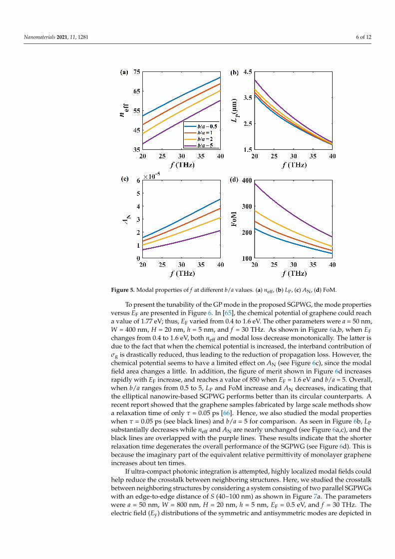
If ultra-compact photonic integration is attempted, highly localized modal fields couldhelp reduce the crosstalk between neighboring structures. Here, we studied the crosstalkbetween neighboring structures by considering a system consisting of two parallel SGPWGswith an edge-to-edge distance of S (40~100 nm) as shown in Figure 7a. The parameterswere a = 50 nm, W = 800 nm, H = 20 nm, h = 5 nm, EF = 0.5 eV, and f = 30 THz. Theelectric field (Ey) distributions of the symmetric and antisymmetric modes are depicted in

Nanomaterials 2021, 11, 1281 7 of 12
Figure 7b,c with S = 40 nm and b/a = 2. Based on the coupled mode theory, the crosstalkis estimated by the coupling length LC, which is the length required for complete powertransfer from one waveguide to the other, and is given by LC = λ0/(2|neff,s - neff,as|), whereneff,s and neff,as denote the real parts of the effective mode indices of the symmetric andantisymmetric modes, respectively [7]. Figure 7d shows the normalized coupling lengths(LC/LP) with respect to S for different b/a values. Usually, when LC/LP approaches 10 (seethe black dashed line), it is assumed that no coupling happens between the neighboringcomponents. When LC/LP reaches 10, the corresponding edge-to-edge distance are about44.0, 55.5, 61.7, and 64.0 nm for b/a = 0.5, 1, 2, and 5, respectively. It is worth noting thatwhen S is above 64 nm, LC/LP is always larger than 10, which indicates that the proposedSGPWG shows extremely low crosstalk between neighboring components and is suitablefor ultra-compact photonics integration.
Nanomaterials 2021, 11, x FOR PEER REVIEW 7 of 12
Figure 6. Modal properties of EF at different b/a values. (a) neff, (b) LP, (c) AN, (d) FoM. Note that the black lines overlap the purple lines in (a) and (c).
If ultra-compact photonic integration is attempted, highly localized modal fields could help reduce the crosstalk between neighboring structures. Here, we studied the crosstalk between neighboring structures by considering a system consisting of two parallel SGPWGs with an edge-to-edge distance of S (40~100 nm) as shown in Figure 7a. The parameters were a = 50 nm, W = 800 nm, H = 20 nm, h = 5 nm, EF = 0.5 eV, and f = 30 THz. The electric field (Ey) distributions of the symmetric and antisymmetric modes are depicted in Figure 7b,c with S = 40 nm and b/a = 2. Based on the coupled mode theory, the crosstalk is estimated by the coupling length LC, which is the length required for complete power transfer from one waveguide to the other, and is given by LC = λ0/(2|neff,s - neff,as|), where neff,s and neff,as denote the real parts of the effective mode indices of the symmetric and antisymmetric modes, respectively [7]. Figure 7d shows the normalized coupling lengths (LC/LP) with respect to S for different b/a values. Usually, when LC/LP approaches 10 (see the black dashed line), it is assumed that no coupling happens between the neighboring components. When LC/LP reaches 10, the corresponding edge-to-edge distance are about 44.0, 55.5, 61.7, and 64.0 nm for b/a = 0.5, 1, 2, and 5, respectively. It is worth noting that when S is above 64 nm, LC/LP is always larger than 10, which indicates that the proposed SGPWG shows extremely low crosstalk between neighboring components and is suitable for ultra-compact photonics integration.
Figure 6. Modal properties of EF at different b/a values. (a) neff, (b) LP, (c) AN, (d) FoM. Note thatthe black lines overlap the purple lines in (a) and (c).
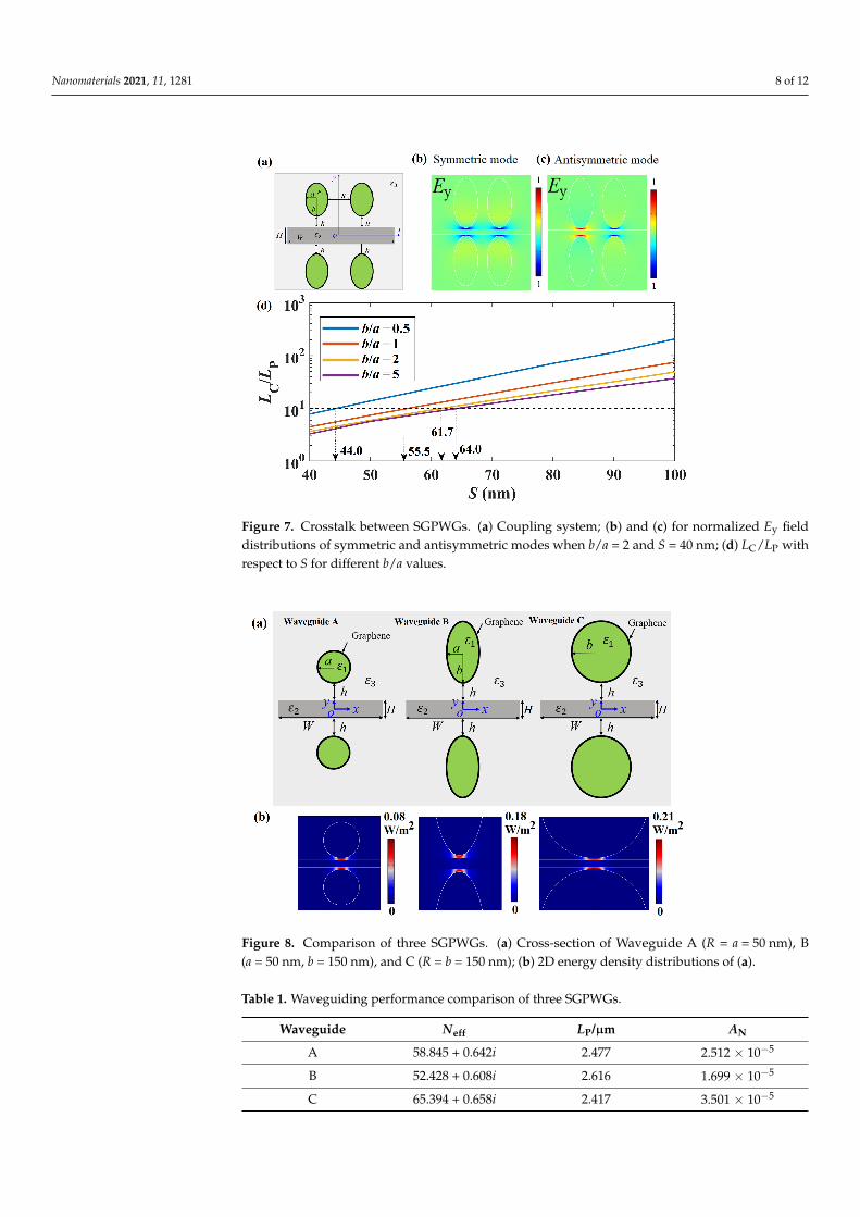
Next, we briefly compare the mode characteristics among three different kinds ofwaveguides, including circular nanowire-based SGPWGs with R = a (Waveguide A)and R = b (Waveguide C), and an elliptical nanowire-based SGPWG (Waveguide B). Theschematics of the three SGPWGs are shown in Figure 8a, and we set a = 50 nm, b = 150 nm,W = 400 nm, h = 5 nm, H = 20 nm, EF = 0.5 eV, and f = 30 THz. Figure 8b shows the 2Denergy density distributions of the fundamental mode in three SGPWGs. The results showthat Waveguide B exhibits much stronger energy confinement than Waveguides A and C,which can be intuitively seen from Table 1 (lower AN). As shown in Table 1, the plasmonmode in Waveguide B has the smallest normalized mode area and largest LP comparedwith the other waveguides.
Nanomaterials 2021, 11, 1281 8 of 12Nanomaterials 2021, 11, x FOR PEER REVIEW 8 of 12
Figure 7. Crosstalk between SGPWGs. (a) Coupling system; (b) and (c) for normalized Ey field distributions of symmetric and antisymmetric modes when b/a = 2 and S = 40 nm; (d) LC/LP with respect to S for different b/a values.
Next, we briefly compare the mode characteristics among three different kinds of waveguides, including circular nanowire-based SGPWGs with R = a (Waveguide A) and R = b (Waveguide C), and an elliptical nanowire-based SGPWG (Waveguide B). The schematics of the three SGPWGs are shown in Figure 8a, and we set a = 50 nm, b = 150 nm, W = 400 nm, h = 5 nm, H = 20 nm, EF = 0.5 eV, and f = 30 THz. Figure 8b shows the 2D energy density distributions of the fundamental mode in three SGPWGs. The results show that Waveguide B exhibits much stronger energy confinement than Waveguides A and C, which can be intuitively seen from Table 1 (lower AN). As shown in Table 1, the plasmon mode in Waveguide B has the smallest normalized mode area and largest LP compared with the other waveguides.
Figure 8. Comparison of three SGPWGs. (a) Cross-section of Waveguide A (R = a = 50 nm), B (a = 50 nm, b = 150 nm), and C (R = b = 150 nm); (b) 2D energy density distributions of (a).
Figure 7. Crosstalk between SGPWGs. (a) Coupling system; (b) and (c) for normalized Ey fielddistributions of symmetric and antisymmetric modes when b/a = 2 and S = 40 nm; (d) LC/LP withrespect to S for different b/a values.
Nanomaterials 2021, 11, x FOR PEER REVIEW 8 of 12
Figure 7. Crosstalk between SGPWGs. (a) Coupling system; (b) and (c) for normalized Ey field distributions of symmetric and antisymmetric modes when b/a = 2 and S = 40 nm; (d) LC/LP with respect to S for different b/a values.
Next, we briefly compare the mode characteristics among three different kinds of waveguides, including circular nanowire-based SGPWGs with R = a (Waveguide A) and R = b (Waveguide C), and an elliptical nanowire-based SGPWG (Waveguide B). The schematics of the three SGPWGs are shown in Figure 8a, and we set a = 50 nm, b = 150 nm, W = 400 nm, h = 5 nm, H = 20 nm, EF = 0.5 eV, and f = 30 THz. Figure 8b shows the 2D energy density distributions of the fundamental mode in three SGPWGs. The results show that Waveguide B exhibits much stronger energy confinement than Waveguides A and C, which can be intuitively seen from Table 1 (lower AN). As shown in Table 1, the plasmon mode in Waveguide B has the smallest normalized mode area and largest LP compared with the other waveguides.
Figure 8. Comparison of three SGPWGs. (a) Cross-section of Waveguide A (R = a = 50 nm), B (a = 50 nm, b = 150 nm), and C (R = b = 150 nm); (b) 2D energy density distributions of (a).
Figure 8. Comparison of three SGPWGs. (a) Cross-section of Waveguide A (R = a = 50 nm), B(a = 50 nm, b = 150 nm), and C (R = b = 150 nm); (b) 2D energy density distributions of (a).
Table 1. Waveguiding performance comparison of three SGPWGs.
Waveguide Neff LP/µm AN
A 58.845 + 0.642i 2.477 2.512 × 10⁻⁵
B 52.428 + 0.608i 2.616 1.699 × 10⁻⁵
C 65.394 + 0.658i 2.417 3.501 × 10⁻⁵

Nanomaterials 2021, 11, 1281 9 of 12
Finally, we briefly introduce the fabrication process of the SGPWG. Recent reports [67,68]showed that graphene-coated elliptical nanowires can be experimentally made by coating adielectric nanowire with a monolayer of graphene due to van der Waals forces. Then, basedon modern semiconductor fabrication technology, the substrate silica can be deposited ontop of the buffer layer [69]. After that, one GCNW is placed on the silica substrate, then theGCNW is covered by silica deposition with a thickness of 2b + h. Next, a silicon layer with athickness of H (about 10 nm) could be deposited on top of the silica using plasma-enhancedchemical vapor deposition (PECVD) technology [70]. Then, h-thick silica is deposited onthe silicon layer before transferring another GCNW. Finally, the second GCNW is coveredby silica deposition with a thickness of over 2b.
4. Conclusions
In summary, a symmetric graphene plasmon waveguide is proposed and investigated.The simulation results show that a normalized mode field area of ∼10-5 and a figure ofmerit of ~400 can be achieved by optimizing the parameters. The mode characteristicscould be dynamically tuned by changing the chemical potential of graphene by a DC biasvoltage or chemical doping. By varying the ratio of b/a, the simulation results show thatelliptical nanowire-based SGPWGs (b/a > 1) show better performance compared withthe cases of b/a ≤1 in terms of LP, AN, and FoM. In addition, crosstalk analysis suggeststhat the proposed SGPWGs have extremely small energy couplings between neighboringcomponents, even at a separation distance of 64 nm. These findings could have potentialapplications for ultra-compact photonic integration and subwavelength optoelectronicdevices in the mid-infrared band.
Author Contributions: Conceptualization, D.T.; writing—original draft preparation, D.T.; Y.W.;writing—review and editing, Y.W.; T.X.; visualization, H.W.; Q.S.; supervision, D.T.; Y.T. All authorshave read and agreed to the published version of the manuscript.
Funding: This work was supported by the Key Scientific Research Project of Henan College(21A140029), the Young Backbone Teacher Training Program of Zhengzhou Normal University(QNGG-20774), the Open Research Fund of Zhengzhou Normal University, and the Scientific Re-search Starting Foundation of Zhengzhou Normal University.
Institutional Review Board Statement: Not applicable.
Informed Consent Statement: Not applicable.
Data Availability Statement: The data presented in this study are available on request from thecorresponding author.
Conflicts of Interest: The authors declare no conflict of interest.
References1. Oulton, R.F.; Sorger, V.J.; Genov, D.A.; Pile, D.F.P.; Zhang, X. A hybrid plasmonic waveguide for subwavelength confinement and
long-range propagation. Nat. Photon. 2008, 2, 496–500. [CrossRef]2. Cheben, P.; Halir, R.; Schmid, J.H.; Atwater, H.A.; Smith, D.R. Subwavelength integrated photonics. Nature 2018, 560, 565–572.
[CrossRef]3. Verhagen, E.; Polman, A.; Kuipers, L.K. Nanofocusing in laterally tapered plasmonic waveguides. Opt. Express 2008, 16, 45–57.
[CrossRef] [PubMed]4. Yang, L.; Li, P.; Li, Z. Plasmonic polarization beam splitting based on single silver nanowire. Opt. Express 2019, 27, 3851–3860.
[CrossRef] [PubMed]5. Lu, F.; Zhang, W.; Huang, L.; Liang, S.; Mao, D.; Gao, F.; Mei, T.; Zhao, J. Mode evolution and nanofocusing of grating-coupled
surface plasmon polaritons on metallic tip. Opto-Electron. Adv. 2018, 1, 180010. [CrossRef]6. Moreno, E.; Rodrigo, S.G.; Bozhevolnyi, S.I.; Martín-Moreno, L.; García-Vidal, F.J. Guiding and focusing of electromagnetic fields
with wedge plasmon polaritons. Phys. Rev. Lett. 2008, 100, 023901. [CrossRef] [PubMed]7. Veronis, G.; Fan, S. Crosstalk between three-dimensional plasmonic slot waveguides. Opt. Express 2008, 16, 2129–2140. [CrossRef]8. Gao, H.; Cao, Q.; Zhu, M.; Teng, D.; Shen, S. Nanofocusing of terahertz wave in a tapered hyperbolic metal waveguide. Opt.
Express 2014, 22, 32071–32081. [CrossRef]

Nanomaterials 2021, 11, 1281 10 of 12
9. Zhang, Q.; Hao, H.; Ren, J.; Zhang, F.; Gong, Q.; Gu, Y. A quantum phase gate capable of effectively collecting photons based on agap plasmon structure. Nanoscale 2020, 12, 10082–10089. [CrossRef]
10. Steinberger, B.; Hohenau, A.; Ditlbacher, H.; Stepanov, A.L.; Drezet, A.; Aussenegg, F.R.; Leitner, A.; Krenn, J.R. Dielectric stripeson gold as surface plasmon waveguides. Appl. Phys. Lett. 2006, 88, 094104. [CrossRef]
11. Krasavin, A.V.; Zayats, A.V. Three-dimensional numerical modeling of photonic integration with dielectric-loaded SPP waveg-uides. Phys. Rev. B 2008, 78, 045425. [CrossRef]
12. Han, Z.; Radko, I.P.; Mazurski, N.; Desiatov, B.; Beermann, J.; Albrektsen, O.; Levy, U.; Bozhevolnyi, S.I. On-chip detection ofradiation guided by dielectric-loaded plasmonic waveguides. Nano Lett. 2015, 15, 476–480. [CrossRef] [PubMed]
13. Dai, D.; He, S. A silicon-based hybrid plasmonic waveguide with a metal cap for a nano-scale light confinement. Opt. Express2009, 17, 16646–16653. [CrossRef]
14. Chen, L.; Zhang, T.; Li, X.; Huang, W. Novel hybrid plasmonic waveguide consisting of two identical dielectric nanowiressymmetrically placed on each side of a thin metal film. Opt. Express 2012, 20, 20535–20544. [CrossRef] [PubMed]
15. Alam, M.Z.; Aitchison, J.S.; Mojahedi, M. A marriage of convenience: Hybridization of surface plasmon and dielectric waveguidemodes. Laser Photonics Rev. 2014, 8, 394–408. [CrossRef]
16. Zhang, L.; Pan, C.; Zeng, D.; Yang, Y.; Yang, Y.; Junxian, M. A hybrid-plasmonic-waveguide-based polarization-independentdirectional coupler. IEEE Access 2020, 8, 134268–134275. [CrossRef]
17. Teng, D.; Cao, Q.; Wang, K. An extension of the generalized nonlocal theory for the mode analysis of plasmonic waveguides attelecommunication frequency. Journal of Optics 2017, 19, 055003. [CrossRef]
18. Tuniz, A.; Bickerton, O.; Diaz, F.J.; Kasebier, T.; Kley, E.B.; Kroker, S.; Palomba, S.; de Sterke, C.M. Modular nonlinear hybridplasmonic circuit. Nat. Commun. 2020, 11, 2413. [CrossRef] [PubMed]
19. Huang, T.J.; Yin, L.Z.; Zhao, J.; Du, C.H.; Liu, P.K. Amplifying evanescent waves by dispersion-induced plasmons: Defying thematerials limitation of superlens. ACS Photonics 2020, 7, 2173–2181. [CrossRef]
20. Gao, Y.; Shadrivov, I.V. Second harmonic generation in graphene-coated nanowires. Opt. Lett. 2016, 41, 3623–3626. [CrossRef][PubMed]
21. Barnes, W.L.; Dereux, A.; Ebbesen, T.W. Surface plasmon subwavelength optics. Nature 2003, 424, 824–830. [CrossRef]22. Novoselov, K.S.; Fal, V.I.; Colombo, L.; Gellert, P.R.; Schwab, M.G.; Kim, K. A roadmap for graphene. Nature 2012, 490, 192–200.
[CrossRef] [PubMed]23. Fan, Y.C.; Shen, N.H.; Zhang, F.L.; Zhao, Q.; Wu, H.J.; Fu, Q.H.; Wei, Z.Y.; Li, H.Q.; Soukoulis, C.M. Graphene plasmonics: A
platform for 2D Optics. Adv. Opt. Mater. 2019, 7, 1800537. [CrossRef]24. Teng, D.; Wang, K.; Li, Z. Graphene-coated nanowire waveguides and their applications. Nanomaterials 2020, 10, 229. [CrossRef]
[PubMed]25. Zheng, K.; Yuan, Y.F.; He, J.J.; Gu, G.Q.; Zhang, F.; Chen, Y.; Song, J.; Qu, J.L. Ultra-high light confinement and ultra-long
propagation distance design for integratable optical chips based on plasmonic technology. Nanoscale 2019, 11, 4601–4613.[CrossRef]
26. Shan, H.; Yu, Y.; Wang, X.; Luo, Y.; Zu, S.; Du, B.; Han, T.Y.; Li, B.W.; Li, Y.; Wu, J.R.; et al. Fang, Z. Direct observation of ultrafastplasmonic hot electron transfer in the strong coupling regime. Light Sci. Appl. 2019, 8, 9. [CrossRef] [PubMed]
27. He, X.; Liu, F.; Lin, F.; Xiao, G.; Shi, W. Tunable MoS2 modified hybrid surface plasmon waveguides. Nanotechnology 2018, 30,125201. [CrossRef] [PubMed]
28. Jiang, Y.; Shi, C.; Wang, J. A hybrid plasmonic terahertz waveguide with ridge structure base on Bulk-Dirac-semimetal. Opt.Commun. 2020, 475, 126239. [CrossRef]
29. He, X.; Liu, F.; Lin, F.; Lin, F.; Shi, W. Tunable 3D Dirac-semimetals supported Mid-IR hybrid plasmonic waveguides. Opt. Lett.2021, 46, 472–475. [CrossRef]
30. Dereshgi, S.A.; Liu, Z.; Aydin, K. Anisotropic localized surface plasmons in borophene. Opt. Express 2020, 28, 16725–16739.[CrossRef] [PubMed]
31. Lian, C.; Hu, S.Q.; Zhang, J.; Cheng, C.; Yuan, Z.; Gao, S.; Meng, S. Integrated plasmonics: Broadband dirac plasmons inborophene. Phys. Rev. Lett. 2020, 125, 116802. [CrossRef] [PubMed]
32. Wang, J.; Xing, Z.; Chen, X.; Cheng, Z.Z.; Li, X.J.; Liu, T. Recent progress in waveguide-integrated graphene photonic devices forsensing and communication applications. Front. Phys. 2020, 8, 37. [CrossRef]
33. Yu, P.; Fesenko, V.I.; Tuz, V.R. Dispersion features of complex waves in a graphene-coated semiconductor nanowire. Nanophotonics2018, 7, 925–934. [CrossRef]
34. Saeed, M.; Ghaffar, A.; Alkanhal, M.A.S.; Alqahtani, A.H.; Khan, Y.; ur Rehman, S. Plasmon modes supported by metamaterial-filled monolayer graphene cylindrical waveguides. J. Opt. Soc. Am. B 2020, 37, 3515–3525. [CrossRef]
35. Xing, R.; Jian, S. Numerical analysis on the multilayer nanoring waveguide pair. IEEE Photon. Technol. Lett. 2016, 28, 2779–2782.[CrossRef]
36. Teng, D.; Wang, K.; Li, Z.; Zhao, Y. Graphene-coated nanowire dimers for deep subwavelength waveguiding in mid-infraredrange. Opt. Express 2019, 27, 12458–12469. [CrossRef]
37. Wu, D.; Tian, J. Study on the plasmonic characteristics of bow-tie type graphene-coated nanowire pair. Optik 2018, 156, 689–695.[CrossRef]

Nanomaterials 2021, 11, 1281 11 of 12
38. Wang, X.; Wang, J.; Ma, T.; Liu, H.; Wang, F. Plasmonic characteristics of suspended graphene-coated wedge porous siliconnanowires with Ag partition. Chin. Phys. B 2021, 30, 014207. [CrossRef]
39. Teng, D.; Wang, K. Theoretical analysis of terahertz dielectric–loaded graphene waveguide. Nanomaterials 2021, 11, 210. [CrossRef][PubMed]
40. Jabbarzadeh, F.; Habibzadeh-Sharif, A. High performance dielectric loaded graphene plasmonic waveguide for refractive indexsensing. Opt. Commun. 2021, 479, 126419. [CrossRef]
41. Zhu, J.; Jiang, F.; Yunbai, Q. Sense of surface plasmon polarization waveguide of graphene. Plasmonics 2019, 14, 1903–1910.[CrossRef]
42. Liao, B.; Guo, X.; Hu, H.; Liu, N.; Chen, K.; Yang, X.; Dai, Q. Ultra-compact graphene plasmonic filter integrated in a waveguide.Chin. Phys. B 2018, 27, 094101. [CrossRef]
43. Xu, Y.; Li, F.; Kang, Z.; Huang, D.; Zhang, X.; Tam, H.-Y.; Wai, P.K.A. Hybrid graphene-silicon based polarization-insensitiveelectro-absorption modulator with high-modulation efficiency and ultra-broad bandwidth. Nanomaterials 2019, 9, 157. [CrossRef]
44. Hao, R.; Jiao, J.; Peng, X.; Zhen, Z.; Dagarbek, R.; Zou, Y.; Li, E. Experimental demonstration of a graphene-based hybridplasmonic modulator. Opt. Lett. 2019, 44, 2586–2587. [CrossRef] [PubMed]
45. Liu, J.P.; Zhai, X.; Xie, F.; Wang, L.L.; Xia, S.X.; Li, H.J.; Luo, X.; Shang, X.J. Analytical model of mid-infrared surface plasmonmodes in a cylindrical long-range waveguide with double-layer graphene. J. Lightwave Technol. 2017, 35, 1971–1979. [CrossRef]
46. Hajati, M.; Hajati, Y. Investigation of plasmonic properties of graphene multilayer nano-ribbon waveguides. Appl. Opt. 2016, 55,1878–1884. [CrossRef] [PubMed]
47. Wang, Y.; Liu, H.; Wang, S.; Cai, M.; Ma, L. Optical transport properties of graphene surface plasmon polaritons in mid-infraredband. Crystals 2019, 9, 354. [CrossRef]
48. Ctyroky, J.; Petráek, J.; Kuzmiak, V.; Kwiecien, P.; Richter, I. Silicon waveguides with graphene: Coupling of waveguide mode tosurface plasmons. J. Opt. 2020, 22, 095801. [CrossRef]
49. Chen, X.; Wang, Y.; Xiang, Y.; Jiang, G.; Wang, L.; Bao, Q.; Zhang, H.; Liu, Y.; Wen, S.; Fan, D. A broadband optical modulatorbased on a graphene hybrid plasmonic waveguide. J. Lightwave Technol. 2016, 34, 4948–4953. [CrossRef]
50. Hasan, K.B.M.R.; Islam, M.A.; Alam, M.S. Design of a broadband single mode hybrid plasmonic waveguide incorporating siliconnanowire. Opt. Mater. Express 2020, 10, 2783–2799. [CrossRef]
51. Hajati, M.; Hajati, Y. High-performance and low-loss plasmon waveguiding in graphene-coated nanowire with substrate. J. Opt.Soc. Am. B 2016, 33, 2560–2565. [CrossRef]
52. Hajati, M.; Hajati, Y. Plasmonic characteristics of two vertically coupled graphene-coated nanowires integrated with substrate.Appl. Opt. 2017, 56, 870–875. [CrossRef]
53. Sun, M.; Tian, J.; Lan, X.; He, Z.; Liu, J. Transmission properties of two vertically coupled double-graphene-coated nanowiresintegrated with substrate. Optik 2019, 185, 242–247. [CrossRef]
54. Teng, D.; Guo, J.; Yang, Y.; Ma, W.; Wang, K. Study of modal properties in graphene-coated nanowires integrated with substrates.Appl. Phys. B 2020, 126, 173. [CrossRef]
55. Teng, D.; Yang, Y.; Guo, J.; Ma, W.; Tang, Y.; Wang, K. Efficient guiding mid-infrared waves with graphene-coated nanowire basedplasmon waveguides. Res. Phys. 2020, 17, 103169. [CrossRef]
56. Teng, D.; Wang, K.; Huan, Q.; Chen, W.; Li, Z. High-performance light transmission based on graphene plasmonic waveguides. J.Mater. Chem. C 2020, 8, 6832–6838. [CrossRef]
57. Chandler-Horowitz, D.; Amirtharaj, P.M. High-accuracy, midinfrared (450 cm− 16ω 6 4000 cm− 1) refractive index values ofsilicon. J. Appl. Phys. 2005, 97, 123526. [CrossRef]
58. Yang, X.; Liu, X.; Yu, S.; Gan, L.; Zhou, J.; Zeng, Y. Permittivity of undoped silicon in the millimeter wave range. Electronics 2019,8, 886. [CrossRef]
59. Yu, H.; Wang, H.; Xiong, Q.; Mei, J.; Zhang, Y.; Wang, Y.; Lai, J.; Chen, C. Photothermal switch of sub-microsecond response: Amonolithic-integrated ring resonator and a metasurface absorber in silicon photonic crystals. Opt. Lett. 2020, 45, 1806–1809.
60. Ono, M.; Hata, M.; Tsunekawa, M.; Nozaki, K.; Sumikura, H.; Chiba, H.; Notomi, M. Ultrafast and energy-efficient all-opticalswitching with graphene-loaded deep-subwavelength plasmonic waveguides. Nat. Photon. 2020, 14, 37–43. [CrossRef]
61. Nikitin, A.Y.; Alonso-González, P.; Hillenbrand, R. Efficient coupling of light to graphene plasmons by compressing surfacepolaritons with tapered bulk materials. Nano Lett. 2014, 14, 2896–2901. [CrossRef] [PubMed]
62. Buckley, R.; Berini, P. Figures of merit for 2D surface plasmon waveguides and application to metal stripes. Opt. Express 2007, 15,12174–12182. [CrossRef] [PubMed]
63. Said, A.; Atia, K.S.R.; Obayya, S.S.A. On modeling of plasmonic devices: Overview. J. Opt. Soc. Am. B 2020, 37, A163–A174.[CrossRef]
64. Caridad, J.M.; Winters, S.; McCloskey, D.; Duesberg, G.S.; Donegan, J.F.; Krstic, V. Hot-volumes as uniform and reproduciblesers-detection enhancers in weakly-coupled metallic nanohelices. Sci. Rep. 2017, 7, 45548. [CrossRef]
65. Kanahashi, K.; Tanaka, N.; Shoji, Y.; Maruyama, M.; Jeon, I.; Kawahara, K.; Ishihara, M.; Hasegawa, M.; Ohta, H.; Ago, H.; et al.Formation of environmentally stable hole-doped graphene films with instantaneous and high-density carrier doping via aboron-based oxidant. npj 2D Mater. Appl. 2019, 3, 44. [CrossRef]
66. Whelan, P.R.; Shen, Q.; Zhou, B.; Serrano, I.G.; Kamalakar, M.V.; Mackenzie, D.M.; Ji, J.; Huang, D.; Shi, H.; Luo, D.; et al. Fermivelocity renormalization in graphene probed by terahertz time-domain spectroscopy. 2D Mater. 2020, 7, 035009. [CrossRef]

Nanomaterials 2021, 11, 1281 12 of 12
67. Cao, T.; Li, Y.; Tian, L.; Liang, H.; Qin, K. Fast switching “On/Off” chiral surface plasmon polaritons in graphene-coatedGe2Sb2Te5 nanowire. ACS Appl. Nano Mater. 2018, 1, 759–767. [CrossRef]
68. Chen, B.; Meng, C.; Yang, Z.; Li, W.; Lin, S.; Gu, T.; Guo, X.; Wang, D.; Yu, S.; Wong, C.W.; et al. Graphene coated ZnO nanowireoptical waveguides. Opt. Express 2014, 22, 24276–24285. [CrossRef]
69. Vitanov, P.; Ivanova, T.; Dikov, H. Low-temperature deposition of ultrathin SiO2 films on Si substrates. J. Phys. Conf. Ser. 2014,514, 012010. [CrossRef]
70. Flöry, N.; Ma, P.; Salamin, Y.; Emboras, A.; Taniguchi, T.; Watanabe, K.; Leuthold, J.; Novotny, L. Waveguide-integrated van derWaals heterostructure photodetector at telecom wavelengths with high speed and high responsivity. Nat. Nanotechnol. 2020, 15,118–124. [CrossRef]