Mechanisms of doping graphene
15
arXiv:1003.0624v1 [cond-mat.mtrl-sci] 2 Mar 2010 Mechanisms of doping graphene H. Pinto 1 , R. Jones 1 , J. P. Goss 2 , P. R. Briddon 2 1 School of Engineering, Mathematics and Physical Sciences, University of Exeter, EX4 4QL, UK 2 School of Electrical, Electronic and Computer Engineering, Newcastle University, Newcastle upon Tyne, NE1 7RU, UK March 2, 2010 Abstract We distinguish three mechanisms of doping graphene. Density func- tional theory is used to show that electronegative molecule like F4- TCNQ and electropositive metals like K dope graphene p- and n-type respectively. These dopants are expected to lead to a decrease in carrier mobility arising from Coulomb scattering but without any hysteresis effects. Secondly, a novel doping mechanism is exhibited by Au which dopes bilayer graphene but not single layer. Thirdly, electrochemical doping is effected by redox reactions and can result in p-doping by humid atmospheres and n-doping by NH 3 and toluene. 1 Introduction The type and concentration of carriers in graphene can be controlled by adsorbates or substrates which transfer charge to graphene. p-type electronic doping results from a disparity between the work function of graphene and the electron affinity of the adsorbate. In the sim- plest case this is caused by a difference between the highest occupied molecular level (HOMO) and the lowest unoccupied molecular level (LUMO) of the adsorbate and graphene. This alignment as we shall see can depend on the substrate as we shall show that Au dopes bilayer graphene but is ineffective for single layer graphene. Electrochemical doping results from redox reactions near the graphene surface. The timescales for the two types of doping is different since electronic dop- ing occurs spontaneously while electrochemical doping requires longer times to overcome reaction and diffusion barriers. Hysteresis effects 1
-
Upload
independent -
Category
Documents
-
view
1 -
download
0
Transcript of Mechanisms of doping graphene

arX
iv:1
003.
0624
v1 [
cond
-mat
.mtr
l-sc
i] 2
Mar
201
0
Mechanisms of doping graphene
H. Pinto1, R. Jones1, J. P. Goss2, P. R. Briddon2
1School of Engineering, Mathematics and Physical Sciences,
University of Exeter, EX4 4QL, UK2School of Electrical, Electronic and Computer Engineering,
Newcastle University, Newcastle upon Tyne, NE1 7RU, UK
March 2, 2010
Abstract
We distinguish three mechanisms of doping graphene. Density func-tional theory is used to show that electronegative molecule like F4-TCNQ and electropositive metals like K dope graphene p- and n-typerespectively. These dopants are expected to lead to a decrease in carriermobility arising from Coulomb scattering but without any hysteresiseffects. Secondly, a novel doping mechanism is exhibited by Au whichdopes bilayer graphene but not single layer. Thirdly, electrochemicaldoping is effected by redox reactions and can result in p-doping byhumid atmospheres and n-doping by NH3 and toluene.
1 Introduction
The type and concentration of carriers in graphene can be controlledby adsorbates or substrates which transfer charge to graphene. p-typeelectronic doping results from a disparity between the work functionof graphene and the electron affinity of the adsorbate. In the sim-plest case this is caused by a difference between the highest occupiedmolecular level (HOMO) and the lowest unoccupied molecular level(LUMO) of the adsorbate and graphene. This alignment as we shallsee can depend on the substrate as we shall show that Au dopes bilayergraphene but is ineffective for single layer graphene. Electrochemicaldoping results from redox reactions near the graphene surface. Thetimescales for the two types of doping is different since electronic dop-ing occurs spontaneously while electrochemical doping requires longertimes to overcome reaction and diffusion barriers. Hysteresis effects
1

for graphene based field effect devices can also be expected in electro-chemical doping since the concentration of the reactants can change ata rate slower than the change in gate voltages.
Electropositive elements like metals are good candidates for elec-tronic n-type doping of graphene. Molecular beam deposition of tran-sition metal clusters, Ti, Fe and Pt, has shown that these metals effectn-doping of graphene whereas bulk deposition of Pt dopes graphene p-type[1]. Electronic doping on graphene was also demonstrated with Katoms deposited at low temperatures (20K) on graphene in ultrahighvacuum (UHV)[2]. Synchrotron-based high resolution photoemissionspectroscopy (PES) showed that graphene can be made p-type by thedeposition of tetrafluoro-tetracyanoquinodimethane (F4-TCNQ). Be-cause of the molecular separation of the adsobate and graphene, allthese dopants are expected to lead to a decrease in carrier mobilityarising from Coulomb scattering without any hysteresis effects.
Exposure of graphene to a humid atmosphere or gaseous nitrogendioxide leads to p-type behaviour, while ammonia leads to n-type be-haviour [3]. A great surprise is that it was found, in particular experi-mental conditions, gaseous toluene leads to n-doping of graphene[4], incontradiction with theoretical calculations which predict no transfer ofcharge between graphene and the toluene molecule [12]. In this paperdensity functional calculations are used to investigate the transfer ofcharge between graphene and adsorbates. A electrochemical model fordoping of graphene is also presented.
2 Method
The electronic ground state of graphene with different adsorbates wascalculated using spin-optimised density functional theory as imple-mented in the AIMPRO code[5, 6]. The exchange correlation po-tential was described using the local density approximation (LDA).The core electron were treated using the Hartwigsen Goedecker Hut-ter (HGH) pseudopotencials[7]. The orbitals of the valence electronsconsist of independent s−, p−, d− like Gaussian functions centred onatoms[8]. The electronic levels were filled using Fermi-Dirac statis-tics with kBT=0.01 eV and a metallic filling. The Brillouin zonewas sampled with a grid of 8×8×1 k-points within the Monkhorst-Pack scheme[9]. Charge densities were Fourier-transformed using planewaves with an energy cut-off of 200 Ha. The spin-populations of thecell were optimised by starting from random spin distributions. Weused two different graphene unit cells, 4×4×1 and 6×6×1, enclosing32 and 72 carbon atoms, respectively. During the relaxation all theatoms were allowed to move to their equilibrium positions. The in-fluence of the cell size was also studied with larger supercells and the
2

band structure obtained and the consequent charge transfer were verysimilar.
3 Electronic doping
The geometry of the relaxed F4-TCNQ molecule was found to be ingood agreement with experimental results for its precursor TCNQ [10].The electron affinity, the difference between the LUMO and the vac-uum level, was found to be 5.25 eV in agreement with an experimentalmeasurement of 5.2 eV[11]. This deep LUMO level when comparedwith the work function of graphene ∼ 4.5 suggest that F4-TCNQ is agood candidate to act as an electronic acceptor on graphene.
The F4-TCNQ molecule was placed on top of a 72 carbon atomsgraphene supercell, 6×6×1, and during the relaxation all the atomswere allowed to move. In the minimum energy configuration the moleculeremain parallel to the graphene layer with a interplanar separation of3.1 A. The binding energy was found to be 1.26 eV which is probablyoverestimated as a result of the LDA approximation.
Figure 1 a) and b) shows respectively the electronic band structuresof pristine graphene and graphene with an adsorbed molecule. Becauseof band folding, the Dirac point, where the π and π∗ bonding and anti-bonding levels of graphene meet, occurs at Γ instead of the K pointin the 6×6×1 graphene supercell used here. Comparison of the twoelectronic band structures shows that when the molecule is placed ontop of graphene, the Fermi level is shifted to lie below the Dirac point,and a new filled flat band appears which is related to the adsorbate.This suggests transfer of negative charge from graphene to F4-TCNQThis is supported by an analysis of the wavefunction shown in Figure 2a) of the level marked A in Figure 1 b). This shows that the new filledband is strongly localised on the F4-TCNQ molecule. In addition, theempty level marked B, which was occupied in graphene, is delocalisedover the graphene layer. This confirms that charge transfer betweengraphene and F4-TCNQ occurs. The position of the Fermi-level indi-cates about 0.3 electrons are transferred from graphene to a moleculeof F4-TCNQ.
To study the doping properties of metals, a single atom of Au and Krespectiverly were placed on graphene in the three obvious adsorptionsites: above the centre of the graphene hexagonal ring, above a C-Cbond and above the carbon atom. In the case of Au the minimumenergy configuration was found to be 2.27 A on top of a carbon atomwhereas K sits 2.42 A directly above the middle of a hexagon optimisingthe number of K-C bonds. Thus the K atom is strongly bound tographene with a binding energy estimated to be 1.51 eV in contrastwith the 0.65 eV estimated for a Au atom. This is in part due to their
3

a)
−2.0
−1.5
−1.0
−0.5
0.0
0.5
1.0
1.5
2.0
KΓMK
Ene
rgy
(eV
)
k
b)
−2.0
−1.5
−1.0
−0.5
0.0
0.5
1.0
1.5
2.0
KΓMK
Ene
rgy
(eV
)
k
A
B
Figure 1: (Colour online) Band structure (eV) of a) pristine graphene andb) F4-TCNQ on top of graphene plotted in the vicinity of the Fermi energyalong the high symmetry branches of the graphene Brillouin-zone. TheFermi level is set to zero. Full lines (red) denote occupied states whiledashed lines (blie) show empty levels. The Fermi level is placed at zero.The curves shows the unoccupied F4-TCNQ levels around 0 eV becomeoccupied near the Dirac point indicating charge transfer. Colour online
4

a)
b)
Figure 2: (Colour online) Plot of the wavefunction of the a) HOMO levelat Γ marked A in figure 2b) shows strong localisation on F4-TCNQ and theb) LUMO at Γ marked as B in figure 2a) shows strong delocalisation of api-bonding orbital over graphene but avoids F4-TCNQ. Red and blue lobesare of equal amplitude and opposite sign.
5
−4.0
−3.0
−2.0
−1.0
0.0
1.0
2.0
ΓMKΓ
Ene
rgy
(eV
)
k
A
B
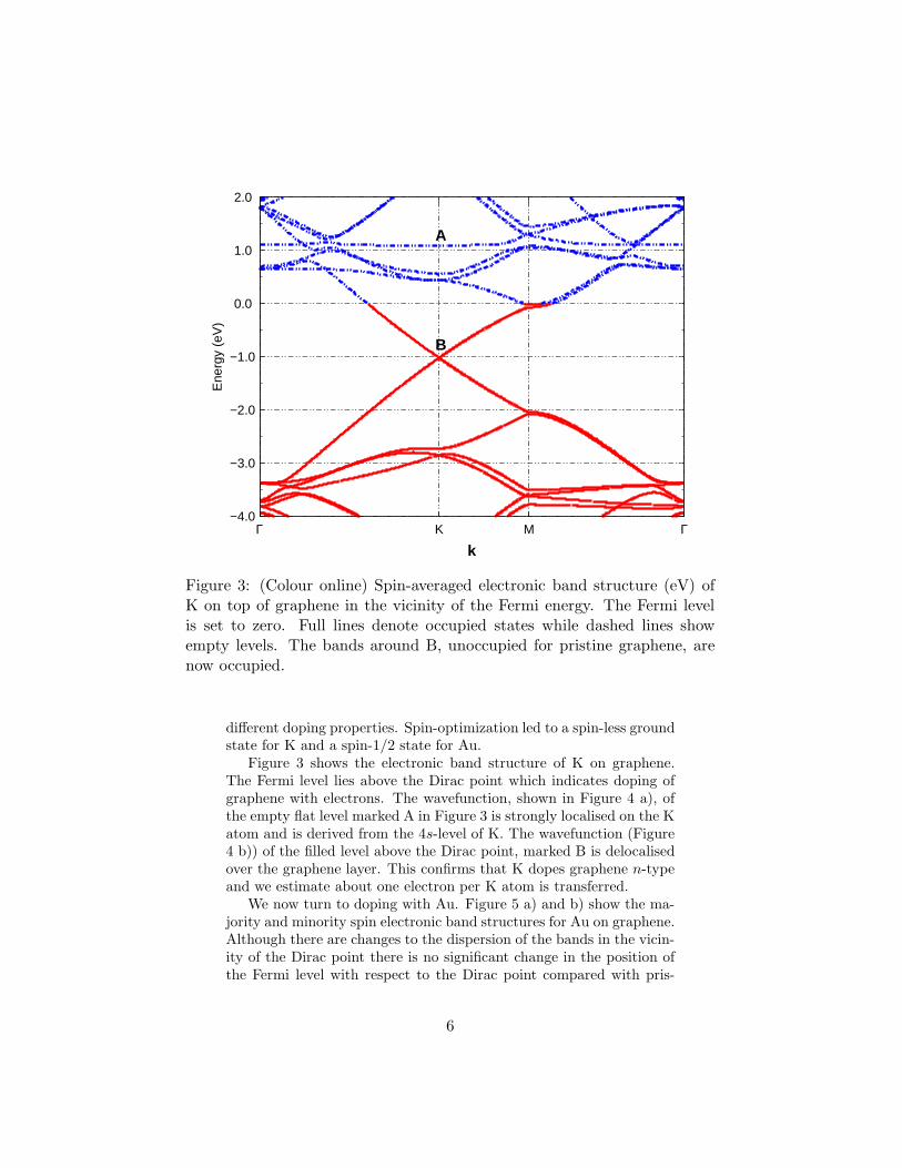
Figure 3: (Colour online) Spin-averaged electronic band structure (eV) ofK on top of graphene in the vicinity of the Fermi energy. The Fermi levelis set to zero. Full lines denote occupied states while dashed lines showempty levels. The bands around B, unoccupied for pristine graphene, arenow occupied.
different doping properties. Spin-optimization led to a spin-less groundstate for K and a spin-1/2 state for Au.
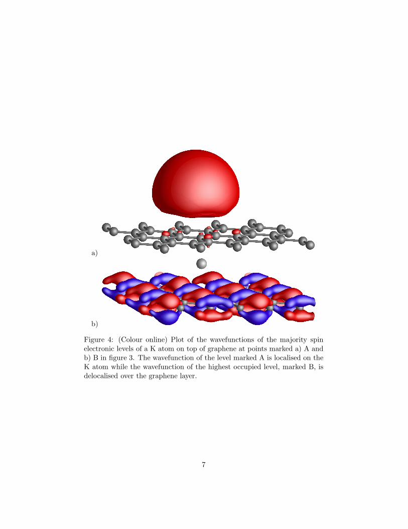
Figure 3 shows the electronic band structure of K on graphene.The Fermi level lies above the Dirac point which indicates doping ofgraphene with electrons. The wavefunction, shown in Figure 4 a), ofthe empty flat level marked A in Figure 3 is strongly localised on the Katom and is derived from the 4s-level of K. The wavefunction (Figure4 b)) of the filled level above the Dirac point, marked B is delocalisedover the graphene layer. This confirms that K dopes graphene n-typeand we estimate about one electron per K atom is transferred.
We now turn to doping with Au. Figure 5 a) and b) show the ma-jority and minority spin electronic band structures for Au on graphene.Although there are changes to the dispersion of the bands in the vicin-ity of the Dirac point there is no significant change in the position ofthe Fermi level with respect to the Dirac point compared with pris-
6
a)
b)
Figure 4: (Colour online) Plot of the wavefunctions of the majority spinelectronic levels of a K atom on top of graphene at points marked a) A andb) B in figure 3. The wavefunction of the level marked A is localised on theK atom while the wavefunction of the highest occupied level, marked B, isdelocalised over the graphene layer.
7
tine graphene. This implies that there is no significant charge transferbetween Au and graphene.
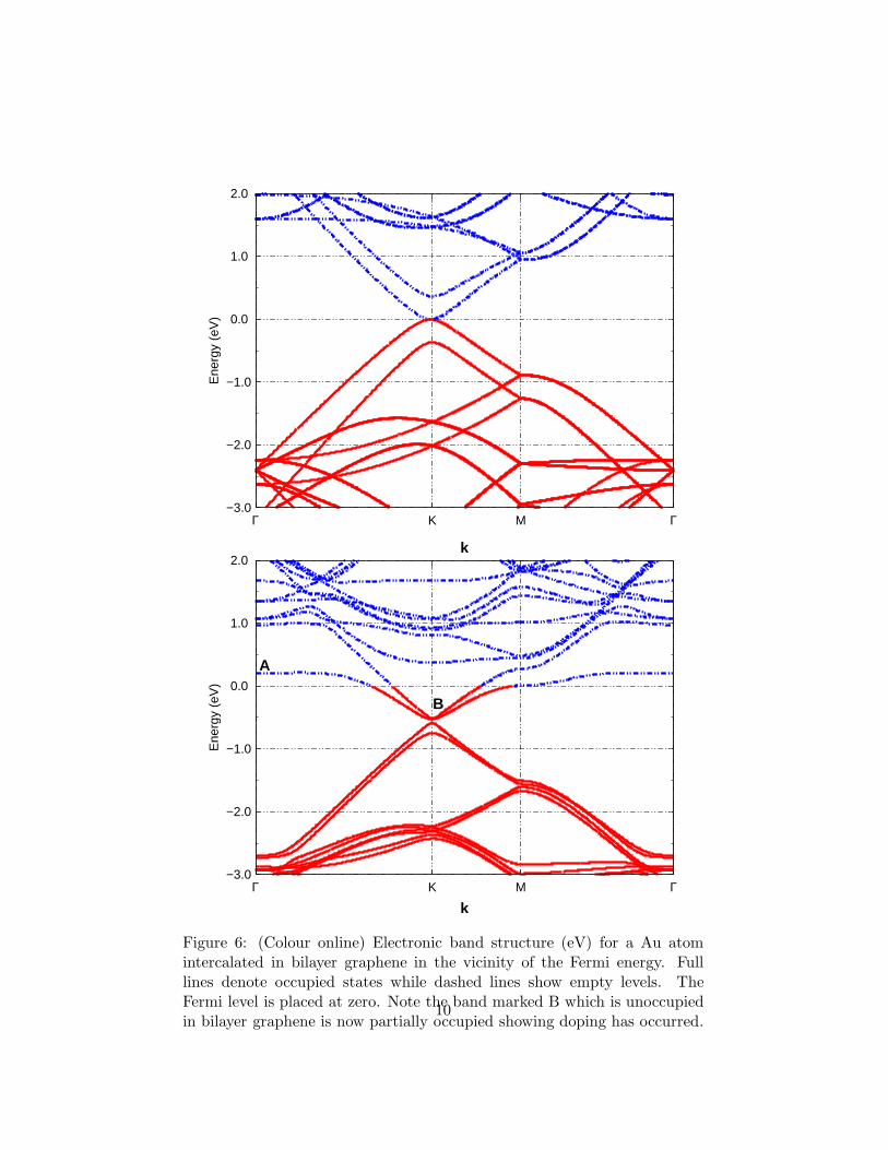
To study the effect of additional graphene layers, a single Au atomwas placed between the AB stacked graphene bilayer. The relaxedground state was spin-less and the Au atom occupied a site nearlymidway between the two graphene layers and 2.14 A directly abovea carbon atom in the lower layer and directly below the middle ofthe hexagon of the top layer. The separation between the graphenelayers increased to approximately 4.5 A. The graphene sheets do notappear to appreciably distort. Figure 6 a) and b) show the electronicband strucuture of a pristine graphene bilayer and a graphene bilayerintercalated with Au atoms. As for single layer graphene, the highestoccupied and lowest empty bands touch at the Dirac point but thelinear dispersion is lost. However, when the Au atom is placed betweenthe graphene layers, the Fermi level is shifted above the Dirac point.An analyis of the wavefunction shows the flat level far from the K point,marked as A, results from the 6s Au level. When the 6s level crossesthe π∗ bands of graphene, they hybridise and charge is transferred tographene effecting n-type doping. The level marked as B in Figure 6,is delocalised over graphene and this level is now occupied, and unlikethe case when the second graphene sheet was absent. We suggestthat the effect of a second graphene layer is to compress the Au 6s-wavefunction with a consequent upward shift of the level. The sameeffect was observed when ther second graphene layer was replaced bya toluene molecule [12].
4 Electrochemical doping
Another type of doping involves electrochemical redox reactions ofgraphene with water and adsorbates. It has been reported that ex-posure of graphene to a humid atmosphere or NO2 results in p-dopingwhereas exposure to gaseous NH3 [3] and toluene results in n-doping[4]. It is important to realise that other carbon based materials canexhibit similar effects. Diamond, whose surface has been treated withhydrogen which reduces considerable its work function, can also bedoped p-type by exposure to a humid atmosphere [13]. The effect issuppressed by NH3 and enhanced by NO2 [14]. Similar effects areseen in carbon nanotubes [15, 16]. These types of doping cannot beexplained by an electronic mechanism involving direct transfer of elec-trons from say toluene to graphene as the ionisation energy of tolueneis ∼ 6 eV [17] and greatly exceeds the work function of graphene. Thetransfer doping model has similar difficulties in the case of NH3. How-ever, atmospheric doping has been suggested as being due to the directtransfer of charge between graphene and defects in layers of ice on top
8

a)
−3.0
−2.0
−1.0
0.0
1.0
2.0
3.0
ΓMKΓ
Ene
rgy
(eV
)
k b)
−3.0
−2.0
−1.0
0.0
1.0
2.0
3.0
ΓMKΓ
Ene
rgy
(eV
)
k
Figure 5: (Colour online) Spin-polarised band structures (eV) of Au in thevicinity of the Fermi energy. (a) Majority spin band structure, and (b)minority spin band structure. The Fermi level is set to zero. Full linesdenote occupied states while dashed lines show empty levels.
9
−3.0
−2.0
−1.0
0.0
1.0
2.0
ΓMKΓ
Ene
rgy
(eV
)
k
−3.0
−2.0
−1.0
0.0
1.0
2.0
ΓMKΓ
Ene
rgy
(eV
)
k
A
B
Figure 6: (Colour online) Electronic band structure (eV) for a Au atomintercalated in bilayer graphene in the vicinity of the Fermi energy. Fulllines denote occupied states while dashed lines show empty levels. TheFermi level is placed at zero. Note the band marked B which is unoccupiedin bilayer graphene is now partially occupied showing doping has occurred.
10
of the SiO2 substrate [18]. Nevertheless, this mechanism could not ex-plain the surface doping of diamond as SiO2 is not present. Instead weargue here that the doping effects due to the atmosphere, NO2 or N2O4,NH3 and toluene on graphene that lead to little change, or an increase,in carrier mobility are all examples of electrochemical redox reactionsoccurring in aqueous layers in contact with graphene. A similar theorywill also be applicable to nanotubes and already has been invoked fordiamond [19]. The similar properties of diamond films, nanotubes andgraphene arise from their similar work functions although the largeband gap of diamond excludes the possibility of n-type doping.
The assumption that a water layer is in contact with graphene isa non-trivial one as theory has indicated that diamond and grapheneare hydrophobic. We are inclined to the view that for graphene andnanotubes, likely places for water deposits are at the interfaces betweengraphene and SiO2. Kelvin probe microscopy and X-ray spectroscopyhave shown four or five water layers exist on the surface of SiO2 filmsgrown on Si [20] and there have been FTIR observations of overtones ofvibrations of water molecules [21] It is also widely believed that watercan exists in voids in a-SiO2 [22] and would be resistant to thermalanneals if the voids are small. For diamond, we suppose water is foundat places where the H termination has been replaced by electrophilicOH or oxygen groups. However, further work is required on this point.
Redox reactions are reactions occurring in aqueous solution involv-ing changes in the charge states of the participants. The net chargechange can be transferred to a electrode which in our case is graphene.Whether such reactions occur require that the change in the total Gibbsfree energy is negative (described as a spontaneous reaction) and thatthe barriers are sufficiently small that the reactions can occur at roomtemperature. Tables of ∆G for a reaction in which unit charge is re-moved to or added from vacuum are available [23] but barrier heightsare unknown and it must be assumed that they are sufficiently low.The total Gibbs free energy change is then ∆G + W for p-doping or∆G−W for n-doping. Here W is the work function of graphene.
It has been argued that the p-doping of diamond is due to theelectrochemical reduction of O2 in the presence of water as in
O2 + 2H2O + 4e = 4OH−.
The reaction is spontaneous with the electron being transferred fromthe valence band of diamond and the formation of OH− groups [19].A current carrying hole is created near the diamond surface. We nowshow that an identical reaction is spontaneous for graphene. We con-sider the process occurs by removal of a electron from graphene toinfinity followed by trapping of the electron by O2 and the subsequentreaction with water. The extraction of the electron from graphene re-quires the expenditure of energy equal to its work function W . This
11

has been measured for graphite in air to be 4.5 eV [24]. This valueis close to 4.9 eV found for hydrogenated diamond [25] and we expectthe same work function for graphene [26]. The similarlities of the workfunction of diamond, graphite and nanotubes explains why the sameredox theory pertains to all three materials. Now ∆G is the free en-ergy for the molecular reaction with the charge brought brought fromvacuum and can be written as −eE − 4.4 eV where E is the electrodepotential relative to a hydrogen electrode. The reaction is assumedto involve molar concentrations of reactants and products. Standardelectrode tables give E to be 0.42 V [23]. Thus the total free energychange for a electron to be taken from graphene and to reduce theO2/water couple is -0.42-4.4 +W or -0.3 eV. Thus the reaction whereelectrons are extracted from graphene by oxygen and water is spon-taneous. The above assumes that that molar concentration of OH−
and O2 are present but if this is not the case, then ∆G depends onthe concentrations of OH− and O2 with the reaction being inhibitedin strongly basic conditions. Nernst’s equation gives ∆G to be
∆G = −4.8− 0.059(14− pH + 0.25 log10(pO2)).
Here pO2is the partial pressure of oxygen in atm. Taking this to be 0.21
atm gives ∆G to vary from -4.8 eV for pH = 14 to -5.7 eV for pH =1. Acidic solutions will promote the reaction as the concentration ofOH− is so low. We note that OH− gradually builds up as dopingincreases and might be expected to lead to reduced carrier mobilityas explained above. That this does not happen can be explained ifOH− is either very effectively screened by surrounding SiO2 groupsor is mobile through SiO2. Previous calculations have shown that thelatter is likely: the binding of OH− to the network is only 0.3 eVand thus diffusion through SiO2 could occur at room temperature [22].Moreover, the theory explains the hysteresis effect [27] if the chemicalreaction rates, or diffusion rate for water, oxygen and OH−, are slowerthan the rate of change of gate voltage. For positive gate voltages,the reaction product OH− drifts away from graphene and the lowerhydroxyl concentration there encourages further dissociation of waterand hence greater increases in hole densities in graphene as indeedobserved. [27].
The atmospheric doping effect disappears following vacuum anneal-ing around 200◦C for both graphene and diamond [13]. We supposethis is because of the loss of oxygen and not to the loss of water. This isbecause we require a water layer to explain doping of annealed samplesby gaseous NO2, NH3 and toluene.
It might be thought that the effects of NO2 and NH3 can now beexplained using the same redox couple but taking into account thechanged pH . However this need not be the case and it is possible thatdifferent redox reactions occur especially in anaerobic conditions. A
12

possible reaction involves the reduction of N2O4 as in N2O4 + 2e =2NO−
2 with a electrode potential of E = .87 V [23]. Thus ∆G wouldbe -5.3 eV and certainly could account for p-doping of both grapheneand diamond.
For the oxidation of NH3 or NH4OH we have, 2NH4OH = N2 +2H2O + 6H+ + 6e with E = −0.09 V and yielding ∆G = 4.5 eV.The electron produced by this reaction is transferred to graphene andthe change in the total free energy is ∆G − W . Thus the oxidationreaction leads to the supply of electrons to graphene provided that thework function is greater than 4.5 eV which is just possible. However,we have ignored the basic conditions present as the reaction is inhibitedin acidic conditions. Nernst’s equation gives ∆G ranging from 4.5 eV(pH = 1) to 3.7 eV (pH = 14). Thus the energy cost in removingan electron from aqueous NH3 is 3.7 eV and is easily recovered by itstransfer to graphene. The reaction occurs because of the scarcity ofH+ and a very high N2 bond energy. It is noteworthy that this reactionis used industrially to remove ammonia during waste water treatment.
Finally we turn to toluene which has been found to result in n-typedoping, a pronounced hysteresis effect and enhanced carrier mobil-ity [4]. One possibility is that this involves the redox couple wheretoluene is oxidised to benzyl alcohol. Such a reaction has been re-ported previously [28]. From the tables of free energies [23],∆G forToluene +2OH− = Benzyl alcohol + H2O + 2e is 3.95 eV. Thus theelectrochemical oxidation of toluene to benzyl alcohol is spontaneousas the work functions exceeds 3.95 eV and the liberated electron will betrapped by graphene achieving n-type doping. For negative bias con-dition, OH− will drift through the SiO2 substrate towards graphene,removing a source of scattering centres and leading to an increase inmobility
The reaction depends however on the concentration of OH− in theSiO2 which is very low. Another possibility is the anaerobic oxida-tion of toluene by water. This reaction is known to occur naturallyat room temperature where it is catalysed by microorganisms. Thestandard electrode potential for Toluene + 21 H2O → 7 HCO−
3 +43H+ + 36e is 0.27 V [29]. In nature, the charge exchange takes placewith the Fe2+/Fe3+ couple [29]. Taking into account the standard elec-trode potential of Fe2+/Fe3+ is 0.77 V, this makes the total free energychange for Toluene + 21 H2O + 36 Fe3+ → 7 HCO−
3 +43 H+ +36 Fe2+
to be -1.04 eV per electron. However, the reaction remains exothermicif the Fe2+/Fe3+ couple is replaced by graphene, as then ∆G−W is -0.37 eV. It is worth emphasising that redox reactions are slow and thusgraphene needs to be exposed to toluene for long periods ∼ 1 hour fora doping affect to be seen. Thus the anaerobic conversion of tolueneinto CO2 in the presence of graphene is favoured. To account for amobility increase, we suppose that mobile H+ ions neutralise charged
13

scattering centres present in the undoped graphene.
5 Conclusions
In summary, we conclude there are two types of dopants for graphene.The first which can be called electronic doping occurs when there is adirect exchange of electrons with an adsorbate and graphene. A goodexample is K. Such doping occurs promptly and leads to a reduction incarrier mobility and there should be no hysteresis effects. The second,involving electrochemical doping occurs by redox reactions involvingwater at the interface. This can lead to an increase in carrier mobilitybut requires appreciable times to occur. This leads to hysterisis effects.The assumption that one or both of the charged products OH− or H+
is mobile and responds to the field due to the gate voltage could explainincreases in carrier mobility.
Acknowledgements
The authors are thankful to Derek Palmer for the helpful discussions.
References
[1] K. Pi, K. McCreary, W. Bao, W. Han, Y. F. Chiang, Y. Li, S. Tsai,C. Lau, R. Kawakami, arXiv:0903.2837v2
[2] J. H. Chen, C. Jang, S. Adam, M. S. Fuhrer, E. D. Willams, Nat.Mater. 4 377 (2008)
[3] F. Schedin, A. K. Geim, S. V. Morozov, E. W. Hill, P. Blake, M. I.Katsnelson, and K. S. Novoselov, Nature Materials, 6 652 (2008)
[4] A.A. Kaverzin, F. Withers, A.S. Price, S.M. Strawbridge,A.K. Savchenko, H. Pinto and R. Jones, Unpublished
[5] R. Jones, P. R. Briddon, Semiconductor and Semimetals 51 287(1998)
[6] M. J. Rayson and P. R. Briddon, Computer Physics Communica-
tion 178(2) 128 (2008)
[7] C. Hartwigsen, S. Goedecker and J. Hutter, Phys. Rev. B 58 3641(1998)
[8] J. P. Goss, M. J. Shaw and P. R. Briddon, Topics in Applied
Physics, 104 69 (2007)
[9] H. J. Monkhorst and J. D. Pack, Phys. Rev. B 13 5188 (1976)
[10] H. Pinto, R. Jones, J. P. Goss, P. R. Briddon, J. Phys. Condens.Matter, 21 4002001 (2009)
14

[11] W. Y. Gao and A. Khan, J. Appl. Phys. 94 (2003) 359
[12] H. Pinto, R. Jones, J. P. Goss, P. R. Briddon, Unpublished
[13] F. Maier, M. Riedel, B. Mantel, J. Ristein, and L. Ley, Phys. Rev.Lett., 85 3472 (2000).
[14] J. A. Garrido, A. Hartl, M Dankerl, A Reitinger, M Eickhoff, AHelwig, G Mller, and M. Stutzmann, J. Am. Chem. Soc., 1304177 (2008)
[15] J Kong, N. R. Franklin, C Zhou, M. G. Chapline, S. Peng, K.Cho, H. Dai, Science 287 622 (2000).
[16] K. Bradley, J-C P. Gabriel, M. Briman, A. Star, and G. Gruner,Phys. Rev. Lett. Phys. Rev. Lett. 91 218301 (2003)
[17] P. B. Merkel, P. Luo, J. P. Dinnocenzo, and S. Farid, Journal ofOrganic Chemistry, 74 5163 (2009).
[18] T. O. Wehling, A. I. Lichtenstein, and M. I. Katsnelson, Appl.Phys. Lett., 93 202110 (2008)
[19] V. Chakrapani, J. C. Angus, A. B. Anderson, S. D. Wolter, B. R.Stoner, G. U. Sumanasekera, Science, 312 1424 (2008).
[20] A. Verdaguer, C. Weis, G. Oncins, G. Ketteler, H. Bluhm, andM. Salmeron, Languir, 23 9699 (2007).
[21] I. M. P. Aarts, A. C. R. Pipino, J. P. M. Hoefnagels, W. M. M.Kessels, and M. C. M. van de Sanden, Phys. Rev. Lett. 95, 166104(2005).
[22] T. Bakos, S. N. Rashkeev, and S. T. Pantelides, Phys. Rev B 69195206 (2004).
[23] CRC Handbook of Physics and Chemistry, ed D. R. Lide, 76 edi-tion CRC Press, p8-21 (2005)
[24] W. N. Hansen, and G. J. Hansen, Surf,. Sci., 481 172 (2001).
[25] B. Rezek, C. Sauerer, C. E. Nebel, M. Stutzmann, J. Ristein,L. Ley, E. Snidero and P. Bergonzo, Appl. Phys. Lett., 82 2266(2003).
[26] S. J. Sque, R. Jones, and P. R. Briddon, Phys. Stat. Sol. (a) 204,3078 (2007)
[27] T. Lohmann, K. v. Klitzing, J. H. Smet, arXiv:0903.5430 (2009)
[28] R. Tomat, A. Rigo, J. Appl. Electrochem., 14 1 (1984)
[29] D. R. Loveley, D. J. Lonergan, Applied Environmental Microbi-ology, 56 1858 (1990).
15