
Local charge transfer doping in suspended graphene nanojunctions
11
arXiv:1201.1035v1 [cond-mat.mes-hall] 4 Jan 2012 This line only printed with preprint option Local Charge Transfer Doping in Suspended Graphene Nanojunctions Jeffrey H. Worne, 1 Hemtej Gullapalli, 2 Charudatta Galande, 2 Pulickel M. Ajayan, 2 and Douglas Natelson 3, 1, a) 1) Department of Electrical and Computer Engineering, Rice University, 6100 Main Street, Houston, Texas 77005, USA 2) Department of Mechanical Engineering and Materials Science, Rice University, 6100 Main Street, Houston, Texas 77005, USA 3) Department of Physics and Astronomy, Rice University, 6100 Main Street, Houston, Texas 77005, USA We report electronic transport measurements in nanoscale graphene transistors with gold and platinum electrodes whose channel lengths are shorter than 100 nm, and compare them with transistors with channel lengths from 1 μm to 50 μm. We find a large positive gate voltage shift in charge neutrality point (NP) for transistors made with platinum electrodes but negligible shift for devices made with gold electrodes. This is consistent with the transfer of electrons from graphene into the platinum electrodes. As the channel length increases, the disparity between the measured NP using gold and platinum electrodes disappears. a) Electronic mail: [email protected] 1
-
Upload
independent -
Category
Documents
-
view
3 -
download
0
Transcript of Local charge transfer doping in suspended graphene nanojunctions
arX
iv:1
201.
1035
v1 [
cond
-mat
.mes
-hal
l] 4
Jan
201
2This line only printed with preprint option
Local Charge Transfer Doping in Suspended Graphene Nanojunctions
Jeffrey H. Worne,1 Hemtej Gullapalli,2 Charudatta Galande,2 Pulickel M. Ajayan,2 and
Douglas Natelson3, 1, a)
1)Department of Electrical and Computer Engineering, Rice University,
6100 Main Street, Houston, Texas 77005, USA
2)Department of Mechanical Engineering and Materials Science,
Rice University, 6100 Main Street, Houston, Texas 77005,
USA
3)Department of Physics and Astronomy, Rice University, 6100 Main Street,
Houston, Texas 77005, USA
We report electronic transport measurements in nanoscale graphene transistors with
gold and platinum electrodes whose channel lengths are shorter than 100 nm, and
compare them with transistors with channel lengths from 1 µm to 50 µm. We find a
large positive gate voltage shift in charge neutrality point (NP) for transistors made
with platinum electrodes but negligible shift for devices made with gold electrodes.
This is consistent with the transfer of electrons from graphene into the platinum
electrodes. As the channel length increases, the disparity between the measured NP
using gold and platinum electrodes disappears.
a)Electronic mail: [email protected]
1
Understanding the band alignment between metals and graphene is important in graphene-
based field-effect transistors,1 photovoltaic devices,2 and other experimental graphitic
systems.3 Charge transfer is often seen as undesirable, for example between a Si/SiO2
substrate and graphene.4,5 Selective doping using reactive metal ions6 or chemical species7,8
can tailor graphene’s electrical properties, however, effectively doping it with holes or elec-
trons. Recent work on the metal-graphene interface has focused on scanning photocurrent
measurements9–11 while electrical measurements using 4-probe geometries have examined
the influence of metal contacts on charge transport.12,13
The role of metal contacts in graphene devices has only recently begun to be explored.
The interaction between rolled sheets of graphene − nanotubes − and metals has been well-
studied.14–16 The unique band structure found in graphene,17 however, requires a different
treatment. Charge carriers in graphene behave like massless Dirac fermions.18 As such, they
cause suppressed charge screening and, when in contact with a metal, lead to a long-range
inhomogeneous electrostatic potential19 that can extend for several hundred nanometers
into the bulk.10,20 This can lead to marked changes in charge transport,20,21 p-n junctions
at the metal-graphene interface,2,22 charge density fluctuations near the contacts,23 and, for
particular metals, the formation of a band gap.24
Due to the length scale of charge diffusion, probing charge transfer is possible provided the
electrode separation is no greater than twice the diffusion distance for charge. Experimen-
tally, this should manifest itself as a shift in the charge neutrality point (NP) as the metal
contacts effectively make the local graphene environment n- or p-type. Using a technique
developed previously,25 we are able to fabricate 3-terminal suspended single-layer graphene
transistors with a high aspect ratio (width/length ∼ 300) and channel lengths less than 100
nm. With transport measurements, we measure shifts in the NP in graphene, suggesting
that we are measuring regions of increased charge density over the bulk.
We used degenerately doped p-type silicon with 200 nm of thermally grown oxide, which
serves both as the substrate and the gate. Using two-step electron-beam lithography,
electron-beam evaporation, and lift-off processing, electrodes with w = 20 µm were de-
fined based on the previously mentioned technique with an average channel length of 51 nm.
These short channel electrodes are composed of a 1 nm titanium adhesion layer and 15 nm of
gold or platinum. For comparison, a set of interdigitated electrodes with l = 1− 50 µm and
w = 200 µm were fabricated with gold or platinum as the electrode. Graphene was grown
2
on copper foils and transferred to our substrate/electrodes using poly(methyl methacrylate)
(PMMA) as a transfer medium.26 The quality of the graphene was determined using Raman
spectroscopy and was verified to be single layer. A representative device is shown in Figure
1.
Samples were measured in a variable temperature probe station and data from 300K
to 4K was collected using a HP4145A parameter analyzer. Mobilities were calculated6
by evaluating dσ/dVg = µCg at the largest value of dσ/dVg. Cg is the capacitance per
unit area of the gate, and, since our graphene is suspended, a serial capacitor model is
used incorporating contributions from the oxide and vacuum under the graphene giving
Cg = 7.26 × 10⁻⁸ F cm−2. For both gold and platinum electrodes, the highest values of
mobilities were found at 20K. Note that bias-driven self-heating may be an issue at the
lowest temperatures examined27, though this does not affect the main observations of this
work. For the short channel devices made with gold, µ20K = 4.8 × 102 cm2 / V · s and for
short channel devices with platinum electrodes, µ20K = 3×101 cm2 / V · s. The mobility for
the interdigitated electrode devices was 3.0×103 cm2 / V · s and 1.0×103 cm2 / V · s for the
gold and platinum electrodes, respectively. We note that the measured values of mobility
are well below those traditionally quoted in the literature of ∼ 4000 for graphene fabricated
under similar growth and transfer conditions.26 This is likely caused by defects introduced
during the growth and transfer process or by structural irregularities such as the folds and
ripples visible in Figure 1. Ripples have been found experimentally to increase resistivity
in graphene and limit the mobility of charge carriers.30 The difference in mobilities between
samples with gold or platinum electrodes likely arises from differing conditions during the
growth and transfer process.
We first present data taken from our very short channel length transistors, shown in Figure
2. Figure 2(a) uses gold electrodes and Figure 2(b) uses platinum electrodes. The sets of
devices were prepared via identical methods, suggesting that any contamination should be
common to the two. Both sets of devices were annealed in vacuum for 16 hours at 100◦C
to remove adsorbed contamination. The more aggressive traditional method of annealing
graphene devices at 400◦C could not be used for the Au electrodes in this geometry, because
gold atom mobility led to short circuits. The more robust Pt devices were subsequently
annealed at 400◦C for one hour in Ar/H2; minimal changes were observed from the data
shown in Figure 2, as described below. Significant contamination on graphene requiring
3
higher temperature annealing is less likely to be a concern in the short channel length
transistors due to the small area probed.
From the figure, a dramatic shift in charge NP to a positive voltage can be seen with
graphene on platinum that is not present for graphene on gold. This behavior was seen in
8 additional Pt devices and 9 additional Au devices. Because of differences in the chemi-
cal potential between graphene and gold or platinum, the local charge density will change
as charges move between the metal-graphene interface in order to equilibrate the chemical
potential for electrons across the two differing materials. This will depend on the relative
work functions of graphene and the metal contacts. Because surface adsorbates can cause
shifts in the work function of metals due to intrinsic electric dipole moments,28 it is difficult
to know the true work function of our electrodes. However, as both the gold and platinum
electrodes were handled under similar conditions, it is likely they have similar types of con-
tamination, leading to similar shifts in their work function. Previous scanning potentiometry
experiments29 have shown that Pt films processed in our laboratory continue to exhibit work
functions higher than identically processed Au films, even upon limited exposure to ambient
conditions. This difference in work functions can have notable effects on charge injection,
as has been seen in experiments on conjugated polymers.29 The energy level crossover from
n- to p-type doping in graphene has been calculated to be ∼ 5.4eV.21 This then suggests
the possibility that gold electrodes will transfer electrons into graphene while platinum elec-
trodes will receive electrons from graphene, based on the composite work functions of the
metals and adsorbates.
The data shown in Figure 2 are consistent with charge transfer doping of graphene,
namely in the shift of the NP found in platinum electrodes and the broadening of the Vg−Id
curves.6,31 In the case of the platinum electrodes, the large shift in NP to positive gate voltage
suggests an increase in hole carriers in the region between electrodes. The gold electrodes
appear to have very little doping as the NP stays centered around 0 V. The gate voltage
required to recover the NP can be used to determine the charge density under zero gate bias,
using n = CgVg/e . For gold electrodes, the largest gate voltage required to reach the NP
was Vg = −7V, corresponding to a charge density of 3.2×1012 cm−2 electrons. For identically
processed platinum electrodes, the NP could not be reached with our experimental setup,
so the lower bound is n =2.72×1013 cm−2 holes. Subsequent annealing of the short-channel
Pt devices at 400 ◦C, does not shift the NP to near Vg = 0 in any devices. Five Pt devices
4
out of twenty-seven exhibited some NP shift with this added annealing, with the NP closest
to Vg = 0 occurring at Vg = 38 V, giving n = 1.73 × 1013 cm−2 for that device. However,
the remaining twenty-two Pt devices on that chip do not show a change in NP from the
data in Figure 2. These data strongly suggest that platinum (with possible work function
modifying adsorbates) is a significant donor of holes into graphene, increasing the charge
carrier density by an order of magnitude over that of gold-based devices.
To establish an upper bound on the distance that the transferred charge travels into
graphene, we measured σ(Vg) for our interdigitated electrodes, shown in Figure 3. As the
channel lengths increase for both gold and platinum devices, the influence of the contacts
on the overall charge density of the channel will decrease. Once a maximum channel length
has been exceeded, the charge density in graphene farthest from both contacts will return to
the bulk value. Therefore, in contrast to the short-channel devices, longer channel gold- and
platinum-based electrode devices should have no NP shift relative to each other. Initially,
both types of devices showed a large positive shift in NP toward +Vg likely due to contami-
nation from the fabrication process. Both Au and Pt samples were initially annealed under
the same conditions as the devices shown in Figure 2 (100◦C in vacuum for 16 hours) with
no appreciable change in NP position. The interdigitated electrodes with graphene were
then annealed at 400◦C in an argon/hydrogen gas mixture and annealed again at 100◦C
in vacuum for 16 hours. After the high temperature annealing, the NP in both gold and
platinum devices shifted toward 0 Vg. They each share the same relative shift in NP for
all channel lengths, likely due to additional adsorbates not removed during the annealing
process or to charged impurities in the substrate. Comparing the data in Figure 3 with that
in Figure 2 suggests that the charge transfer distance between metals and our graphene is
less than 500 nm (half the length of our smallest device in this geometry), consistent with
previously reported results.10,20
In conclusion, we have presented electronic transport measurements on suspended
graphene transistors with a sub-100 nm channel length. Significant shifts in NP were
observed in devices made with platinum contacts but not in devices made with gold con-
tacts, suggesting an increase in the local charge density in platinum devices. As the channel
length increases, the NP dissimilarity between gold and platinum electrodes disappears.
These short channel length transistors offer a method for creating suspended graphene
junctions and for creating locally doped regions in graphene.
5

P.M.A. acknowledges funding support from the Office of Naval Research through the
MURI programme on graphene. D. N. and J. H. W. acknowledge support from the National
Science Foundation award ECCS-0901348, and useful discussions with A. A. Fursina.
6
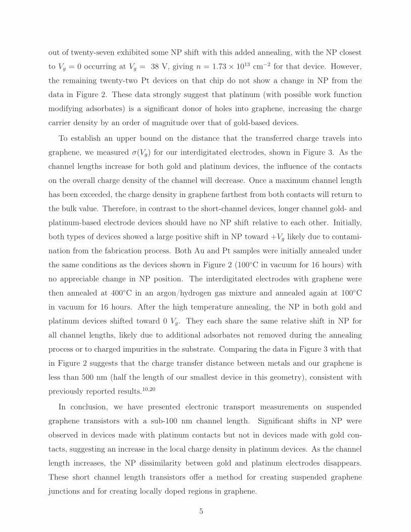
Figure 1. SEM micrograph of graphene on gold electrodes. The electrode separation is 72 nm.
Wrinkles and folds can be followed across the gap, suggesting the graphene is suspended. Inset:
Cartoon illustrating sample geometry.
7

Figure 2. DC transport data from (a) gold (L = 20 nm), µ20K = 4.8 × 102 cm2/V·s, and (b)
platinum (L = 50 nm), µ20K = 3× 101 cm2/V· s, short channel electrodes. The voltage across the
electrodes was fixed at 100 mV. A clear neutrality point evolves in the gold-based devices near Vg
= 0 V but is shifted to +Vg in the platinum-based devices.
8

Figure 3. DC transport data from (a) gold, µ = 3.0×103 cm2/V· s, and (b) platinum µ = 1.0×10
3
cm2/V· s, long channel (1 µm - 50 µm) devices, with bias fixed at 100 mV at 300 K. No visible
difference in the position of the neutrality point is seen between the two samples.
9

REFERENCES
1L. Liao, Y.-C. Lin, M. Bao, R. Cheng, J. Bai, Y. Liu, Y. Qu, K. L. Wang, Y. Huang, and
X. Duan, Nature 467, 305 (2010).
2T. Mueller, F. Xia, and P. Avouris, Nat. Phot. 4, 297 (2010).
3A. K. Geim, Science 324, 1530 (2009).
4K. S. Novoselov, Z. Jiang, Y. Zhang, S. V. Morozov, H. L. Stormer, U. Zeitler, J. C. Maan,
G. S. Boebinger, P. Kim, and A. K. Geim, Science 315, 1379 (2007).
5X. Du, I. Skachko, A. Barker, and E. Y. Andrei, Nat. Nano. 3, 491 (2008).
6J.-H. Chen, C. Jang, S. Adam, M. S. Fuhrer, E. D. Williams, and M. Ishigami, Nat. Phys.
4, 377 (2008).
7X. Wang, X. Li, L. Zhang, Y. Yoon, P. K. Weber, H. Wang, J. Guo, and H. Dai, Science
324, 768 (2009).
8T. O. Wehling, K. S. Novoselov, S. V. Morozov, E. E. Vdovin, M. I. Katsnelson, A. K.
Geim, and A. I. Lichtenstein, Nano Lett. 8, 173 (2008).
9E. J. H. Lee, K. Balasubramanian, R. T. Weitz, M. Burghard, and K. Kern, Nat. Nano.
3, 486 (2008).
10T. Mueller, F. Xia, M. Freitag, J. Tsang, and P. Avouris, Phys. Rev. B 79, 245430 (2009).
11R. S. Sundaram, C. Gomez-Navarro, E. J. H. Lee, M. Burghard, and K. Kern, Appl. Phys.
Lett. 95, 223507 (2009).
12B. Huard, N. Stander, J. Sulpizio, and D. Goldhaber-Gordon, Phys. Rev. B 78, 121402
(2008).
13P. Blake, R. Yang, S. Morozov, F. Schedin, L. Ponomarenko, A. Zhukov, R. Nair, I. Grig-
orieva, K. Novoselov, and A. Geim, Solid State Commun. 149, 1068 (2009).
14A. M. Rao, P. C. Eklund, S. Bandow, and A. Thess, Nature 191, 257 (1997).
15P. Petit, Chem. Phys. Lett. 305, 370 (1999).
16N. Lang and P. Avouris, Phys. Rev. Lett. 84, 358 (2000).
17Y. Zhang, Y.-W. Tan, H. L. Stormer, and P. Kim, Nature 438, 201 (2005).
18K. S. Novoselov, A. K. Geim, S. V. Morozov, D. Jiang, M. I. Katsnelson, I. V. Grigorieva,
S. V. Dubonos, and A. A. Firsov, Nature 438, 197 (2005).
19P. Khomyakov, A. Starikov, G. Brocks, and P. Kelly, Phys. Rev. B 82, 115437 (2010).
20R. Golizadeh-Mojarad and S. Datta, Phys. Rev. B 79, 085410 (2009).
10

21G. Giovannetti, P. Khomyakov, G. Brocks, V. Karpan, J. van den Brink, and P. Kelly,
Phys. Rev. Lett. 101, 026803 (2008).
22P. A. Khomyakov, G. Giovannetti, P. C. Rusu, G. Brocks, J. van den Brink, and P. J.
Kelly, Phys. Rev. B 79, 195425 (2009).
23R. Jalilian, L. A. Jauregui, G. Lopez, J. Tian, C. Roecker, M. M. Yazdanpanah, R. W.
Cohn, I. Jovanovic, and Y. P. Chen, Nanotechnology 22, 295705 (2011).
24A. Varykhalov, M. Scholz, T. Kim, and O. Rader, Phys. Rev. B 82, 121101 (2010).
25A. Fursina, S. Lee, R. G. S. Sofin, I. V. Shvets, and D. Natelson, Appl. Phys. Lett. 92,
113102 (2008).
26X. Li, W. Cai, J. An, S. Kim, J. Nah, D. Yang, R. Piner, A. Velamakanni, I. Jung,
E. Tutuc, et al., Science 324, 1312 (2009).
27J. G. Checkelsky, L. Li, N. P. Ong, Phys. Rev. Lett. 100, 206801 (2008).
28V. De Renzi, R. Rousseau, D. Marchetto, R. Biagi, S. Scandolo, and U. del Pennino, Phys.
Rev. Lett. 95, 046804 (2005).
29B. H. Hamadani, D. A. Corley, J. W. Ciszek, J. M. Tour, and D. Natelson, Nano Lett. 6,
1303 (2006).
30M. I. Katsnelson and A. K. Geim, Phil. Trans. R. Soc. A 366, 195 (2008).
31K. M. McCreary, K. Pi, and R. K. Kawakami, Appl. Phys. Lett. 98, 192101 (2011).
11