Transfer printing of graphene strip from the graphene grown on copper wires
Upload
jntukakinadaCategory
view
1download
0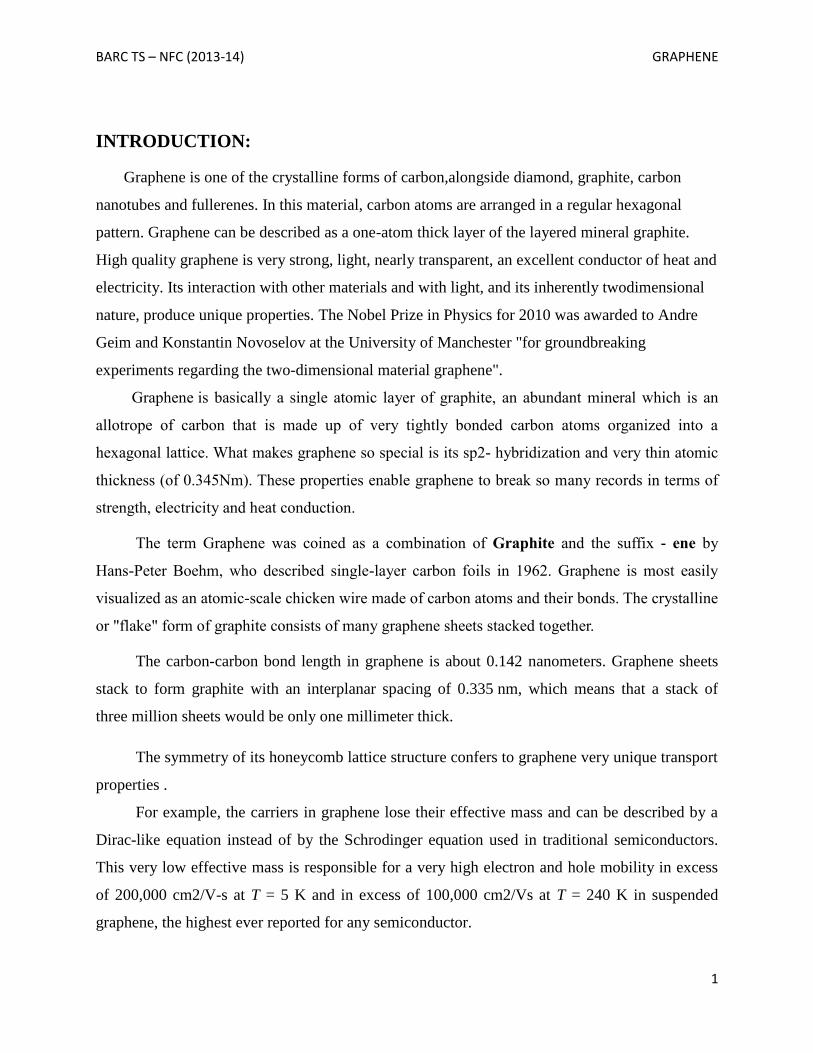
BARC TS – NFC (2013-14) GRAPHENE
1
INTRODUCTION:
Graphene is one of the crystalline forms of carbon,alongside diamond, graphite, carbon
nanotubes and fullerenes. In this material, carbon atoms are arranged in a regular hexagonal
pattern. Graphene can be described as a one-atom thick layer of the layered mineral graphite.
High quality graphene is very strong, light, nearly transparent, an excellent conductor of heat and
electricity. Its interaction with other materials and with light, and its inherently twodimensional
nature, produce unique properties. The Nobel Prize in Physics for 2010 was awarded to Andre
Geim and Konstantin Novoselov at the University of Manchester "for groundbreaking
experiments regarding the two-dimensional material graphene".
Graphene is basically a single atomic layer of graphite, an abundant mineral which is an
allotrope of carbon that is made up of very tightly bonded carbon atoms organized into a
hexagonal lattice. What makes graphene so special is its sp2- hybridization and very thin atomic
thickness (of 0.345Nm). These properties enable graphene to break so many records in terms of
strength, electricity and heat conduction.
The term Graphene was coined as a combination of Graphite and the suffix - ene by
Hans-Peter Boehm, who described single-layer carbon foils in 1962. Graphene is most easily
visualized as an atomic-scale chicken wire made of carbon atoms and their bonds. The crystalline
or "flake" form of graphite consists of many graphene sheets stacked together.
The carbon-carbon bond length in graphene is about 0.142 nanometers. Graphene sheets
stack to form graphite with an interplanar spacing of 0.335 nm, which means that a stack of
three million sheets would be only one millimeter thick.
The symmetry of its honeycomb lattice structure confers to graphene very unique transport
properties .
For example, the carriers in graphene lose their effective mass and can be described by a
Dirac-like equation instead of by the Schrodinger equation used in traditional semiconductors.
This very low effective mass is responsible for a very high electron and hole mobility in excess
of 200,000 cm2/V-s at T = 5 K and in excess of 100,000 cm2/Vs at T = 240 K in suspended
graphene, the highest ever reported for any semiconductor.

BARC TS – NFC (2013-14) GRAPHENE
2
Secondly, graphene is a zero-bandgap material where the conduction and valence bands
touch each other at a point called the Dirac point. In addition to this zero bandgap, the density of
states in graphene is zero at the Dirac point and increases linearly for energies above and below
it, which allows for carrier modulation.
Thirdly, the carriers in graphene are confined to a layer that is only one atom thick. This
allows unprecedented electrostatic confinement, and also makes graphene extremely flexible and
transparent These unique properties of graphene have motivated intense work among physicists
and engineers who have seen in this material new opportunities to improve digital and radio
frequency (RF) electronics, advanced sensors, transparent electronics, low-power switches, solar
cells, and even battery energy storage.
Fig.1 Graphene is a 2D building material for carbon materials of all other dimensionalities. It can
be wrapped up into 0D Fullerene, rolled into 1D nanotube or stacked into 3D graphite .
BARC TS – NFC (2013-14) GRAPHENE
3
Fig.2 Honeycomb structure of graphene
Before monolayer graphene was isolated in 2004, it was theoretically believed that two
dimensional compounds could not exist due to thermal instability when separated. However,
once graphene was isolated, it was clear that it was actually possible, and it took scientists some
time to find out exactly how. After suspended graphene sheets were studied by transmission
electron microscopy, scientists believed that they found the reason to be due to slight rippling in
the graphene, modifying the structure of the material. However, later research suggests that it is
actually due to the fact that the carbon to carbon bonds in graphene are so small and strong that
they prevent thermal fluctuations from destabilizing it.
DEFINITION:
The International Union of Pure and Applied Chemistry (IUPAC) defines grapheme as a
flat monolayer of carbon atoms tightly packed into a two dimensional (2D) honeycomb lattice,
and is a basic building block for graphitic materials of all other dimensionalities. It can be
wrapped up into 0D fullerenes, rolled into 1D nanotubes or stacked into 3D graphite.

BARC TS – NFC (2013-14) GRAPHENE
4
Fig 3 : Freely suspended Graphene layer showing ripples
Fig.4 Graphene structure from TEM

BARC TS – NFC (2013-14) GRAPHENE
5
HISTORY AND EXPERIMENTAL RESEARCH:
The term GRAPHENE first appeared in 1987 to describe single sheets of graphite as one of
the constituents of graphite intercalation compounds (GICs).
In 2003, one ingenious physicist took a block of graphite, some Scotch tape and a lot of
patience and persistence and produced a magnificent new wonder material that is a million times
thinner than paper, stronger than diamond, more conductive than copper. It is called graphene,
and it took the physics community by storm when the first paper appeared the following year.
Geim did research on graphene(in 2007) including discovery of a new class of materials –
free-standing two-dimensional crystals in particular graphene and (in 2008) he discovered and
isolated a single free-standing atomic layer of carbon (graphene) and elucidated its remarkable
electronic properties and also developed (in 2009) the first two-dimensional crystals made of
carbon atoms .
The recent discovery of graphene (Novoselov et al., 2004), a single atomic sheet of
graphite,has ignited intense research activities to explore the electronic properties of this novel
two dimensional (2D) electronic system. Charge transport in graphene differs from that in
conventional 2D electronic systems as a consequence of the conical energy dispersion relation
near the charge neutrality (Dirac) point in the electronic band structure . Field-effect mobility as
high as 15,000 cm2/V.s and a Fermi velocity of ~108 cm/s have been demonstrated at room
temperature (Geim & Novoselov 2007). These properties make graphene a possible candidate for
electronic devices in the future.
Furthermore, calculations show that a graphene sheet is thermodynamically unstable with
respect to other fullerene structures if its size is less than about 20 nm (“graphene is the least
stable structure until about 6000 atoms”) and becomes the most stable one (as within graphite)
only for sizes larger than 24,000 carbon atoms. The flat graphene sheet is also known to be
unstable with respect to scrolling i.e. curling up, which is its lower energy state
In 2008, graphene produced by exfoliation was one of the most expensive materials on
Earth, with a sample that can be placed at the cross section of a human hair costing more than
BARC TS – NFC (2013-14) GRAPHENE
6
$1,000 as of April 2008 (about $100,000,000/cm2). Since then, exfoliation procedures have been
scaled up, and now companies sell grapheme in large quantities. On the other hand, the price of
epitaxial graphene on SiC is dominated by the substrate price, which is approximately $100/cm2
as of 2009.
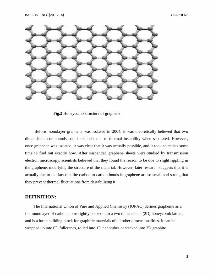
ELECTRONIC STRUCTURE AND TRANSPORT IN GRAPHENE:
The valence electrons of carbon atoms in graphene are sp2 hybridized with the remaining
pz carbon orbitals forming an extended π-electron system that is responsible for the low energy
transport and optical properties of graphene. The carbon atoms are arranged in the form of a
hexagonal honeycomb lattice with two atoms A and B per unit cell.
Fig 5: Left to right: Graphene lattice, electronic bandstructure , linear dispersion at low energies,
pseudospin components, and density of states (DOS) dependence on energy, shape of sp2
hybridised orbitals
The bonding π states form the valence band and the antibonding π* states form the
conduction band. These two bands touch at six points, the so-called Dirac or neutrality points.
Symmetry allows these six points to be reduced to a pair K and K0, which are independent of

BARC TS – NFC (2013-14) GRAPHENE
7
one another. If we limit ourselves to low energies, which are the most relevant in electron
transport, the bands have a linear dispersion E = Vfhk , where Vf is the Fermi velocity. Here, the
band structure can be viewed as two cones touching at the Dirac point. This behavior is the direct
result of the fact that the π and π* states are orthogonal, and as such, can cross smoothly with no
repulsion or bandgap opening. Because of the lack of a bandgap, graphene is usually described
as a zero-gap semiconductor, or better yet, as a semimetal. Furthermore, since the band structure
is symmetric about the Dirac point, electrons and holes in pure, freestanding graphene should
have the same properties. The density of states (DOS) is not constant with energy, as in
conventional two-dimensional electron gas (2 DEG), but rather increases linearly with energy
away from E-Dirac. Taking into account the presence of the two graphene sublattices A and B,
the Hamiltonian that describes the low energy bandstructure in the vicinity of the KðK0Þ points
can be described by a 2-D Dirac relativistic Hamiltonian for massless fermions H ¼ hvF_k.1 In
this Hamiltonian, k is the wavevector measured relative to the KðK0Þ point and the σ’s are Pauli
spinor matrices . This Hamiltonian is well known in particle physics where it is used to describe
massless neutrinos. In the case of graphene, however, the spinor σ does not describe the
particle’s spin. It is rather a two-component vector called pseudospin that gives the relative
amplitude of the electronic wavefunction on the two sublattices A and B, and always points
along the electron momentum k (opposite for holes). If the electron density is all on A, the
pseudospin is ‘‘up,’’ while if on B, σ is ‘‘down.’’ In general, the pseudospin wavefunction is a
linear combination of the ‘‘up’’ and ‘‘down’’ states. Physically, the pseudospin describes the
character (bonding or antibonding) of the underlying molecular orbital.
PROPERTIES:
Graphene differs from most conventional three-dimensional materials. Intrinsic graphene
is a semi-metal or zero-gap semiconductor. Experimental results from transport measurements
show that graphene has a remarkably high electron mobility at room temperature, with reported
values in excess of 15,000 cm2V−1s−1.The mobilities for holes and electrons should be nearly
the same in it. Despite the zero carrier density near the Dirac points, graphene exhibits a
minimum conductivity on the order of 4e2 / h.

BARC TS – NFC (2013-14) GRAPHENE
8
Graphene is a two-dimensional (2D) material with great potential for electronics. With
essentially the same lattice structure as an unwrapped carbon nanotube, graphene shares many of
the advantages of nanotubes, such as the highest intrinsic carrier mobility at room temperature of
any known materials . Recently, it was shown that grapheme devices can exhibit current gain in
the microwave frequency range. Despite intense activities on graphene research, the intrinsic
high-frequency transport properties of graphene transistors have not been systematically studied.
Some of the important useful properties of graphene are discussed below.
ELECTRONIC PROPERTIES :
One of the most useful properties of graphene is that it is a zero-overlap semimetal (with
both holes and electrons as charge carriers) with very high electrical conductivity. Carbon atoms
have a total of 6 electrons; 2 in the inner shell and 4 in the outer shell. The 4 outer shell electrons
in an individual carbon atom are available for chemical bonding, but in graphene, each atom is
connected to 3 other carbon atoms on the two dimensional plane, leaving 1 electron freely
available in the third dimension for electronic conduction. These highly-mobile electrons are
called pi (π) electrons and are located above and below the graphene sheet. This pi orbital’s
overlap and help to enhance the carbon to carbon bonds in graphene. Fundamentally, the
electronic properties of graphene are dictated by the bonding and anti-bonding (the valance and
conduction bands) of these pi orbitals.
Combined research over the last 50 years has proved that at the Dirac point in graphene,
electrons and holes have zero effective mass. This occurs because the energy – movement
relation (the spectrum for excitations) is linear for low energies near the 6 individual corners of
the Brillouin zone. These electrons and holes are known as Dirac fermions, or Graphinos, and the
6 corners of the Brillouin zone are known as the Dirac points. Due to the zero density of states at
the Dirac points, electronic conductivity is actually quite low. However, the Fermi level can be
changed by doping (with electrons or holes) to create a material that is potentially better at
conducting electricity than, for example, copper at room temperature.
BARC TS – NFC (2013-14) GRAPHENE
9
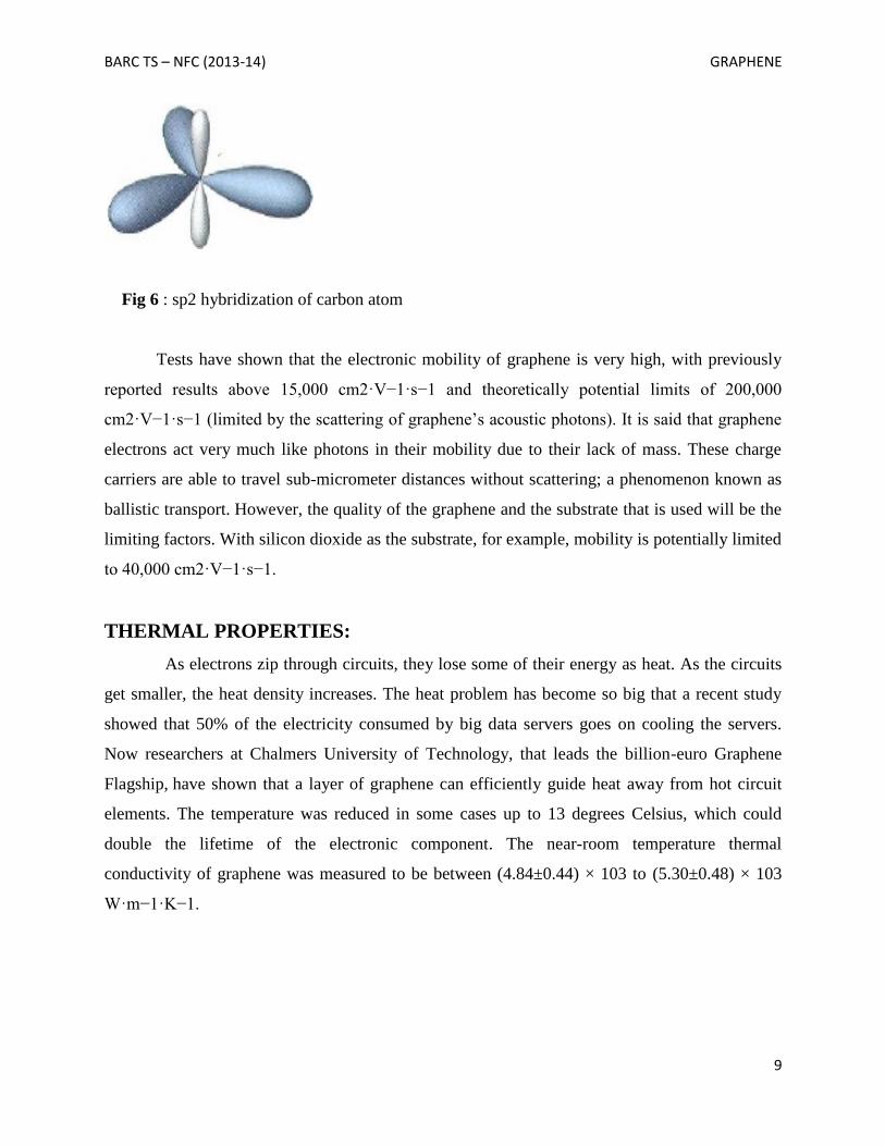
Fig 6 : sp2 hybridization of carbon atom
Tests have shown that the electronic mobility of graphene is very high, with previously
reported results above 15,000 cm2·V−1·s−1 and theoretically potential limits of 200,000
cm2·V−1·s−1 (limited by the scattering of graphene’s acoustic photons). It is said that graphene
electrons act very much like photons in their mobility due to their lack of mass. These charge
carriers are able to travel sub-micrometer distances without scattering; a phenomenon known as
ballistic transport. However, the quality of the graphene and the substrate that is used will be the
limiting factors. With silicon dioxide as the substrate, for example, mobility is potentially limited
to 40,000 cm2·V−1·s−1.
THERMAL PROPERTIES:
As electrons zip through circuits, they lose some of their energy as heat. As the circuits
get smaller, the heat density increases. The heat problem has become so big that a recent study
showed that 50% of the electricity consumed by big data servers goes on cooling the servers.
Now researchers at Chalmers University of Technology, that leads the billion-euro Graphene
Flagship, have shown that a layer of graphene can efficiently guide heat away from hot circuit
elements. The temperature was reduced in some cases up to 13 degrees Celsius, which could
double the lifetime of the electronic component. The near-room temperature thermal
conductivity of graphene was measured to be between (4.84±0.44) × 103 to (5.30±0.48) × 103
W·m−1·K−1.

BARC TS – NFC (2013-14) GRAPHENE
10
MECHANICAL PROPERTIES:
Fig 7: Can put a 4Kg mass (e.g. a cat) on a 1 m2 graphene (if one can make it).
Cartoon taken from Nobel Prize announcement
Another of graphene’s stand-out properties is its inherent strength. Due to the strength of its
0.142 nm long carbon bonds, graphene is the strongest material ever discovered, with an ultimate
tensile strength of 130,000,000,000 Pascals (or 130 gigapascals), compared to 400,000,000 for
A36 structural steel or 375,700,000 for Aramid (Kevlar). Not only is graphene extraordinarily
strong, it is also very light at 0.77milligrams per square metre (for comparison purposes, 1 square
metre of paper is roughly 1000 times heavier). It is often said that a single sheet of graphene
(being only 1 atom thick), sufficient in size enough to cover a whole football field, would weigh
under 1 single gram .
What makes this particularly special is that graphene also contains elastic properties, being
able to retain its initial size after strain. In 2007, Atomic force microscopic (AFM) tests were
carried out on graphene sheets that were suspended over silicone dioxide cavities. These tests
showed that graphene sheets (with thicknesses of between 2 and 8 Nm) had spring constants in
the region of 1-5 N/m and a Young’s modulus (different to that of three-dimensional graphite) of
0.5 TPa. Again, these superlative figures are based on theoretical prospects using graphene that
is unflawed containing no imperfections whatsoever and currently very expensive and difficult to
artificially reproduce, though production techniques are steadily improving, ultimately reducing
costs and complexity.

BARC TS – NFC (2013-14) GRAPHENE
11
Fig 8 :A representation of a diamond tip with a two nm radius indenting into a single atomic
sheet of graphene
OPTICAL PROPERTIES :
Graphene’s ability to absorb a rather large 2.3% of white light is also a unique and
interesting property, especially considering that it is only 1 atom thick. This is due to its
aforementioned electronic properties; the electrons acting like massless charge carriers with very
high mobility. A few years ago, it was proved that the amount of white light absorbed is based on
the Fine Structure Constant, rather than being dictated by material specifics. Adding another
layer of graphene increases the amount of white light absorbed by approximately the same value
(2.3%). Graphene’s opacity of πα ≈ 2.3% equates to a universal dynamic conductivity value of
G= /4ℏ (±2-3%) over the visible frequency range.
Due to these impressive characteristics, it has been observed that once optical intensity
reaches a certain threshold (known as the saturation fluence) saturable absorption takes place
(very high intensity light causes a reduction in absorption). This is an important characteristic
with regards to the mode-locking of fibre lasers. Due to graphene’s properties of wavelength-
insensitive ultrafast saturable absorption, full-band mode locking has been achieved using an
erbium-doped dissipative soliton fibre laser capable of obtaining wavelength tuning as large as
30 nm.

BARC TS – NFC (2013-14) GRAPHENE
12
Fig.9 A single and bilayer sample suspended on a porous membrane. Optical absorbance is
measured at 2.3% per layer. The inset shows the sample design with several apertures.

BARC TS – NFC (2013-14) GRAPHENE
13
METHODS OF EXTRACTION OF GRAPHENE :
Fig 10:
(i) One of the first photographs of isolated graphene. They used the simple technique of ripping
layers from a graphite surface (called as exfoliation) using adhesive tape..
(ii) High resolution scanning electron micrograph image of graphene. Reproduced
with permission from Physics World, Nov 2006, p 1.
(iii) Atomic resolution of graphitic layers extracted using exfoliation method. Reproduced with
permission from Nature Mater., 6, 185 (2007).
There are different ways to extract graphene ,which are listed below and some of them are
discussed.
Exfoliation of Graphite
Epitaxial growth on silicon carbide
Epitaxial growth on metal substrate
Graphite oxide reduction
Growth from metal-carbon melts
Pyrolysis of sodium ethoxide
From graphite by sonication
(i) (ii)
(iii)

BARC TS – NFC (2013-14) GRAPHENE
14
EXFOLIATION
In 2004, the Manchester group obtained graphene by micro-mechanical alleviation of
graphite. They used adhesive tape to repeatedly split graphite crystals into increasingly thinner
pieces (however, filed in 2002 US Patent 6,667,100 describes the process in detail to achieve a
graphite thickness of 0.01 thousandth of an inch). The tape with attached optically transparent
flakes was dissolved in acetone, and, after a few further steps, the flakes including monolayers
were sedimented on a silicon wafer. Individual atomic planes were then hunted with an optical
microscope. A year later, the researchers simplified the technique and started using dry
deposition, avoiding the stage when graphene floated in a liquid.
EPITAXIAL GROWTH ON SILICON CARBIDE :
This method involves heating silicon carbide (SiC) to high temperatures (>1100 °C) under
low pressures (~10−6 torr) to reduce it to graphene. This process produces epitaxial graphene
with dimensions dependent upon the size of the SiC substrate (wafer). Many important graphene
properties have been identified in graphene produced by this method. Extremely large,
temperature-independent mobilities have been observed in SiC-epitaxial graphene. Epitaxial
graphene on SiC can be patterned using standard microelectronics methods.
EPITAXIAL GROWTH ON METAL SUBSTRATES :
This method uses the atomic structure of a metal substrate to seed the growth of the
graphene (epitaxial growth). Graphene grown on ruthenium doesn't typically yield a sample with
a uniform thickness of graphene layers, and bonding between the bottom graphene layer and the
substrate may affect the properties of the carbon layers.[48] On the other hand, graphene grown
on iridium is very weakly bonded, uniform in thickness, and can be made highly ordered.

BARC TS – NFC (2013-14) GRAPHENE
15
GRAPHITE OXIDE REDUCTION :
Graphite oxide reduction was probably historically the first method of graphene
synthesis. P. Boehm reported monolayer flakes of reduced graphene oxide already in 1962.[54]
In this early work existence of monolayer reduced graphene oxide flakes was demonstrated.
Graphite oxide exfoliation can be achieved by rapid heating and yields highly dispersed carbon
powder with a few percent of graphene flakes. Reduction of graphite oxide monolayer films e.g.
by hydrazine, annealing in argon/hydrogen was reported to yield graphene films. However, the
quality of graphene produced by graphite oxide reduction is lower compared to e.g. scotch-tape
graphene due to incomplete removal of various functional groups by existing reduction methods.
GROWTH FROM METAL-CARBON MELTS :
The general idea in this process is to dissolve carbon atoms inside a transition metal
melt at a certain temperature, and then allow the dissolved carbon to precipitate out at lower
temperatures as single layer graphene (SLG).[60] The metal is first melted in contact with a
carbon source. This source could be the graphite crucible inside which the melting process is
carried out or it could be the graphite powder or chunk sources, which are simply placed in
contact with the melt. Keeping the melt in contact with carbon source at a given temperature will
give rise to dissolution and saturation of carbon atoms in the melt based on the binary phase
diagram of metal-carbon. Upon lowering the temperature, solubility of the carbon in the molten
metal will decrease and the excess amount of carbon will precipitate on top of the melt. The
floating layer can be either skimmed or allowed to freeze for removal afterwards.
PYROLYSIS OF SODIUM ETHOXIDE :
A 2008 publication described a process for producing gram-quantities of graphene, by
the reduction of ethanol by sodium metal, followed by pyrolysis of the ethoxide product, and
washing with water to remove sodium salts

BARC TS – NFC (2013-14) GRAPHENE
16
FROM GRAPHITE BY SONICATION :
It consists in dispersing graphite in a proper liquid medium that is then sonicated. Non
exfoliated graphite is eventually separated from graphene by centrifugation. This method was
first proposed by Hernandez et al.[65] who obtained graphene concentration up to 0.01 mg/ml in
N-methyl pyrolidone (NMP).
APPLICATIONS:
A strip of graphene only 10 atoms thick can serve as the basic element in a new type of
memory, making massive amounts of storage in a two-dimensional array by a factor of five,
available for computers, handheld media players, cell phones and cameras.
Device would have many advantages over today’s state-of-the-art flash memory and
other new technologies. The new switches can be controlled by two terminals instead of three, as
in current chips.
If commercialized, a single-atom-thick honeycomb lattice of carbon atoms, can transport
electrons more quickly than other semiconductors, which makes graphene a promising material
for high-speed electronic components such as ranging from cell phones, digital cameras, to super
computers and even this property leads to it’s usage in high frequency devices. Due to its high
frequency, the processing speed of the P.Cs, laptops e.t.c can be greatly increased.
When it comes to fabricating stretchable, transparent electronics, finding a material to
make transistors from has been a significant challenge for researchers. They've explored a variety
of conventional semiconductor materials, including molecules, polymers, and metals, but these
materials tend to have intrinsically poor optical and mechanical properties. These drawbacks
make it difficult to realize a transistor that can maintain its optical and electrical performance
under a high strain. In a new study, researchers have fabricated a stretchable, transparent
graphene-based transistor and found that, due to graphene's excellent optical, mechanical, and

BARC TS – NFC (2013-14) GRAPHENE
17
electrical properties, the transistor overcomes some of the problems faced by transistors made of
conventional semiconductor materials.
Some of the applications in which it can be used are listed below :
IMAGE SENSOR:
Sensor made of graphene that is 1,000 times more sensitive to light than traditional
CMOS or CCD sensors, all while using ten times less energy. Graphene sensor is the first to
detect broad spectrum light, from visible to infrared, with high sensitivity. This makes the sensor
suitable for satellite imaging, infrared cameras, surveillance cameras, and traffic light cameras.
The graphene nano-structures "trap" electrons and hold onto them longer than other sensors,
capturing light better and producing clearer images. The sharp images and lower energy use will
eventually lead to cheaper cameras with longer battery life, Graphene sensors will be "at least
five times cheaper" to manufacture.
FLEXIBLE ELECTRONICS :
As the paradigm of electronic devices changes toward flexible electronics, the
development of new materials that can stand high strains becomes more and more important. In
particular, flexible transparent electrodes are essential to develop a new type of displays and
solar cells that are flexible, foldable or stretchable . However, the current material for transparent
electrodes such as indium tin oxides (ITO) is not suitable as flexible electrodes due to its
fragility. Graphene, an atom thick carbon materials, is not only highly transparent and
conducting but also extremely flexible, which is expected to replace the use of ITO both for
flexible and non-flexible electronics in the future.

BARC TS – NFC (2013-14) GRAPHENE
18
Fig.11 Flexible circuit using graphene
TOUCHSCREEN :
A capacitive touchscreen panel consists of an insulator such as glass, coated with a
transparent conductor such as graphene. As the human body is also an electrical conductor,
touching the surface of the screen results in a distortion of the screen's electrostatic field,
measurable as a change in capacitance. Different technologies may be used to determine the
location of the touch. The location is then sent to the controller for processing.
Fig. 12 Capacitive touchscreen using graphene

BARC TS – NFC (2013-14) GRAPHENE
19
WATER TREATMENT :
The availability of fresh water is dwindling in many parts of the world, a problem that is
expected to grow with populations. One promising source of potable water is the world’s
virtually limitless supply of seawater, but so far desalination technology has been too expensive
for widespread use. Now a new approach using a different kind of filtration material: sheets of
graphene, a one-atom-thick form of the element carbon, which are far more efficient and
possibly less expensive than existing desalination systems.
In fig.13 it is shown that when water molecules (red and white) and sodium and chlorine
ions (green and purple) in saltwater, on the right, encounter a sheet of graphene (pale blue,
center) perforated by holes of the right size i.e. of about 1nm diameter, the water passes through
(left side), but the sodium and chlorine of the salt are blocked .
Fig.13 Water treatment using graphene membrane

BARC TS – NFC (2013-14) GRAPHENE
20
AEROSPACE :
The use of new and exotic material, graphene, is explored in tailoring and designing
composites to create aircraft structural parts. Faster and lighter aircraft could be built using this
incredible super-thin material. Graphene-polymer composites would be ideal for making
lightweight gasoline tanks. They could also be used to make lighter, more fuel-efficient aircraft
and car parts, as well as stronger wind turbines, medical implants, and sports equipment.
Fig.14 Graphene composites used in aerospace.
OPERATION AS TRANSISTOR :
The dc electrical characteristics of the completed graphene device after the deposition of
the top-gate electrode are shown in Fig.16a. The inset shows the measured current as a function
of (top-gate) voltage VG at a drain bias of VD) 100 mV. Despite the small on/off ratio, the
graphene devices are essentially ambipolar field-effect transistors, as indicated by the “V”-shape
gate dependence in the measured ID-VG curve. Figure 16a shows the n-type output
characteristics, ID-VD, of the graphene transistor at various gate voltages.

BARC TS – NFC (2013-14) GRAPHENE
21
Fig 15.
(a) Optical image of the device layout with ground signal-Ground accesses for the drain and the
gate.
(b) Scanning electron microscopy image of the graphene channel and contacts. The inset shows
the optical image of the as deposited graphene flake (circled area) prior to the formation of
electrodes.
(c) Schematic cross section of the graphene transistor.
.

BARC TS – NFC (2013-14) GRAPHENE
22
Fig.16 characteristics of a graphene device
It is found that the top-gated GFETs studied here exhibit a nearly linear ID-VD dependence
up to 1.6 V for the gate voltage ranges measured. This lack of current saturation is due to the fact
that graphene is a zero-gap semiconductor. The high frequency performance of a transistor for
small signal response is mainly determined by the trans-conductance gm=dID/dV. Both the sign
and magnitude of gm are found to be strongly dependent on the gate voltage. To probe the high-
frequency response of the GFET, on chip microwave measurements were carried out using a
HP8510 vector network analyzer up to 10 GHz to obtain the scattering S-parameters that relate
the ac currents and voltages between the drain and the gate of the GFET. The de-embedded S
parameters constitute a complete set of coefficients to describe intrinsic input and output
behaviors of the graphene device and can be used to derive other important electrical properties
such as gain.

BARC TS – NFC (2013-14) GRAPHENE
23
Fig.17
Fig. 17(a) shows the magnitude of all of the four de-embedded S parameters of the GFET
measured at VG =0.5 V and VD=1.6 V as a function of frequency, and the corresponding short
circuit small-signal current gain h21=iD/iG calculated from the measured S parameters is shown
in Figure 17(b).The 1/f dependence of current gain obtained in Fig.17(b) is significant because it
not only validates the high-frequency measurements and the de-embedding procedures used to
extract the intrinsic GFET characteristics but also suggests regular FET-like behaviors for
graphene transistors as a function of frequency. One of the important figures of merit for
characterizing high-frequency transistors is the cutoff frequency fT, defined as the frequency
where the current gain becomes unity (h21=1). In practice, for a transistor possessing the ideal -
20 dB/decade slope for h21, the cutoff frequency fT is determined by the product of h21 and
frequency, i.e., f ·h21(f), over the measured frequency range. For the device shown in Fig 14, the
cutoff frequency fT can be determined by either approach to be 4 GHz. The high-frequency
operation of the graphene transistor is found to be highly dependent on the dc bias condition.
In a FET, the cutoff frequency is given by fT =gm/(2πCG), where CG is the total gate
capacitance. With this relation, a gate capacitance of CG = 72 Ff, GFET, the gate capacitance is
calculated to be ~80 fF. These results show that the high-frequency behavior of these graphene

BARC TS – NFC (2013-14) GRAPHENE
24
transistors can be described as an FET with a static, constant gate capacitance within a
significant portion of the bias range. To investigate the length dependence of fT in graphene
devices, grapheme transistors with various gate lengths were fabricated and investigated for their
high-frequency operations. The maximum fT was found to increase with reduced gate lengths, a
peak cutoff frequency as high as 26 GHz was obtained. It is important to note that while the S
parameters were measured up to 10 GHz.
Fig.18
The current gain in Fig.18 exhibits the expected 1/f dependence for a well-behaved FET, so
that a cutoff frequency fT higher than 10 GHz can be reliably obtained by the product f*h21(f)
over the measured frequency range. The inset of Fig.18 shows the maximum cutoff frequency as
a function of gate length LG measured at a drain bias VD=1.6V. The length dependence of
maximum fT can be fit by fT ~(1/LG )^2.
In summary, the short-circuit current gain showed the ideal 1/f frequency dependence,
confirming the measurement quality and the FET-like behavior for graphene devices. . A peak
cutoff frequency fT as high as 26 GHz was measured for a 150 nm gate graphene transistor,
establishing the state of the art for graphene transistors. These results also indicate that if the
high mobility of graphene can be preserved during the device fabrication process, a cutoff
frequency approaching terahertz may be achieved for graphene FET with a gate length of just 50
nm and carrier mobility of 2000 cm2/(V·s).

BARC TS – NFC (2013-14) GRAPHENE
25
GRAPHENE TRANSISTOR FABRICATION:
Graphene was prepared by mechanical exfoliation on a high resistivity Si substrate (>10
kΩcm) covered by a layer of 300 nm thermal SiO2 and Raman spectroscopy was employed to
count the number of graphene layers. Source and drain electrodes made of 1 nm Ti as the
adhesion layer and 50 nm thick Pd was defined by e-beam lithography and lift-off. A 12 nm
thick Al2O3 layer was then deposited by atomic layer deposition (ALD) at 250 oC as the gate
insulator. In order to form a uniform coating of oxide on graphene, a functionalization layer
consisting of 50 cycles of NO2-TMA (tri methyl aluminum) was first deposited prior to the
growth of gate oxide. This NO2-TMA functionalization layer was essential for the ALD process
to achieve thin (<10 nm) gate dielectrics on graphene without producing pinholes that cause gate
leakage. The dielectric constant of ALD-grown Al2O3 is determined by C-V measurements and
found to be about 7.5. Lastly, 10 nm/50 nm Pd/Au was deposited and patterned to form the top
gate. As shown in the source electrodes were designed to overlap the entire graphene flake in
order to minimize the uncertainty in the de-embedding process for high-frequency S-parameter
measurements.
Fig. 19: Schematic drawing of a typical nanostructure made from a monolayer graphene flake.
The graphene sheet is deposited on a substrate consisting of highly doped silicon (Si++ back
gate) and 295 nm silicon oxide (SiO2). Depositing a Chromium/Gold layer (Cr/Au contact)

BARC TS – NFC (2013-14) GRAPHENE
26
directly on the flake makes an ohmic contact. Metallic top-gates have to be separated from the
flake by thin dielectric insulators (top gate oxide). In the drawing, the top-gate has been cut open
in order to show the graphene structure below. In-plane gates made of graphene (graphene side
gate) are obtained by etching a trench into the graphene sheet.
STRETCHABLE GRAPHENE TRANSISTORS OVERCOME
LIMITATIONS OF OTHER MATERIALS :
When it comes to fabricating stretchable, transparent electronics, finding a material to
make transistors from has been a significant challenge for researchers. They've explored a variety
of conventional semiconductor materials, including molecules, polymers, and metals, but these
materials tend to have intrinsically poor optical and mechanical properties. These drawbacks
make it difficult to realize a transistor that can maintain its optical and electrical performance
under a high strain. In a new study, researchers have fabricated a stretchable, transparent
graphene-based transistor and found that, due to graphene's excellent optical, mechanical, and
electrical properties, the transistor overcomes some of the problems faced by transistors made of
conventional semiconductor materials.
In fact, it is nearly impossible to fabricate transistors that offer both mechanical
stretchability and high optical transparency on unusual substrates such as rubber slabs or
balloons by using conventional materials. In particular, graphene devices have the advantage that
they can be integrated using printing processes at room temperature without vacuum or high-
temperature steps. The capabilities of these systems go far beyond conventional material-based
systems." To fabricate the transistor, the researchers synthesized single layers of graphene and
then stacked them layer by layer on copper foil. Using photolithography and etching techniques,
the researchers patterned some of the transistor's essential elements, including the electrodes and
semiconducting channel, onto the graphene. After transferring these components onto a
stretchable rubber substrate, the researchers printed the remaining components - gate insulators
and gate electrodes - onto the device using stretchable ion gel.
BARC TS – NFC (2013-14) GRAPHENE
27
The researchers found that the graphene-based transistors on rubber substrates had several
attractive features. For instance, the low-temperature printing processes made the fabrication
technique much simpler than techniques that require high-temperature processes. Also,
transistors made of conventional inorganic semiconducting materials cannot be fabricated on
rubber substrates due to their poor mechanical properties, "Stretchable graphene transistors
overcome limitations of other materials." which limits their stretchable range.
The researchers' experimental results confirmed the graphene transistors' good
performance. They showed that the devices could be stretched up to 5% for 1,000 times and still
maintain their good electrical properties. In one experiment, the researchers fabricated the
graphene transistors on a rubber balloon and measured its electrical properties as they inflated
the balloon. When stretched more than 5%, the electrical properties began to degrade, due partly
to microcracks and other defects in the graphene films. "We can make an effort to improve the
range of stretchability and the electronic properties of the current graphene devices and apply
them to various wearable electronics and sensory skins,"
The researchers predict that the graphene transistors could serve as a valuable component
in future transparent and stretchable electronic applications, offering a performance that would
be difficult to achieve using conventional electronic materials. Applications could include
rollable displays, conformal biosensors that shape themselves on an underlying surface, and
others.
"Stretchable electronics could be useful for various current and future applications, such as
wearable displays and communication devices, conformal and stretchable biosensors (brain
sensors, balloon catheters, etc.), sensory skin for robotics, and structural health monitors and eye-
ball cameras,"
"Stretchable interconnects and devices would create foldable, rollable and wearable
displays. Stretchable sensors could be embedded into gloves and clothing without bulkiness.
Surgeon gloves could constantly monitor blood pH and other chemical levels."
SCIENTISTS DEVELOP WORLD'S FASTEST GRAPHENE
TRANSISTOR:

BARC TS – NFC (2013-14) GRAPHENE
28
IBM Scientists from the company ´s T. J. Waston Research Center have
demonstrated the operation of a graphene field-effect transistors at GHz frequencies. Graphene is
a special form of graphite, consisting of a single layer of carbon atoms packed in honeycomb
lattice, similar to an atomic scale chicken wire. With a top gate deisgn and a gate length 150 nm,
the team has achieved a cut-off frequency of 26 GHz for graphene transistors; the highest
frequencies reported so far using this novel non-silicon electronic material.
GRAPHENE PROVIDES EFFICIENT ELECTRONICS COOLING :
A layer of graphene can reduce the working temperature in hotspots inside a processor by
up to 25 percent -- which can significantly extend the working life of computers and other
electronics. This discovery opens the door to increased functionality and continues to push the
boundaries when it comes to miniaturising electronics .Modern electronic systems generate a
great deal of heat, above all due to the constantly increasing demand for more and more
functionality. It is important to be able to remove the heat generated in an efficient way to
maintain the long life of the system. One rule of thumb is that a 10-degree Celsius increase in
working temperature halves the working life of an electronics system. During the study, the
researchers focused on reducing the temperature in the small area where the electronics work
most intensively -- such as inside a processor, for instance. These tiny hotspots are found in all
electronics. Size wise, they are on a micro or nano scale, in other words a thousandth of a
millimeter or smaller. “The normal working temperature in the hotspots we have cooled with a
graphene layer has ranged from 55 to 115 degrees Celsius. We have been able to reduce this by
up to 13 degrees, which not only improves energy efficiency, it also extends the working life of
the electronics." Efficient cooling is a major challenge in many different applications, such as
automotive electronics, power electronics , computers, radio base stations and in various light
emitting diodes, or LED lights. LED devices can have a thermal intensity almost on a par with
the sun, up to 600 W/cm2 due to their extremely small size. Superior cooling of electronics can
deliver tremendous advantages. According to a study in the USA based on data from 2006,
around 50 percent of the total electricity used to run data servers goes on cooling the systems.
Copyright © 2022 FDOKUMEN