Graphene and Graphene Nanomesh Spintronics - MDPI
19
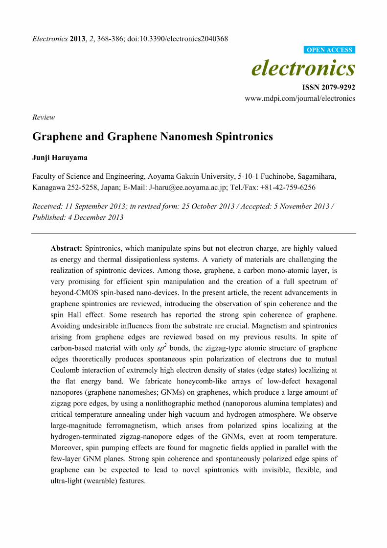
Electronics 2013, 2, 368-386; doi:10.3390/electronics2040368 electronics ISSN 2079-9292 www.mdpi.com/journal/electronics Review Graphene and Graphene Nanomesh Spintronics Junji Haruyama Faculty of Science and Engineering, Aoyama Gakuin University, 5-10-1 Fuchinobe, Sagamihara, Kanagawa 252-5258, Japan; E-Mail: [email protected]; Tel./Fax: +81-42-759-6256 Received: 11 September 2013; in revised form: 25 October 2013 / Accepted: 5 November 2013 / Published: 4 December 2013 Abstract: Spintronics, which manipulate spins but not electron charge, are highly valued as energy and thermal dissipationless systems. A variety of materials are challenging the realization of spintronic devices. Among those, graphene, a carbon mono-atomic layer, is very promising for efficient spin manipulation and the creation of a full spectrum of beyond-CMOS spin-based nano-devices. In the present article, the recent advancements in graphene spintronics are reviewed, introducing the observation of spin coherence and the spin Hall effect. Some research has reported the strong spin coherence of graphene. Avoiding undesirable influences from the substrate are crucial. Magnetism and spintronics arising from graphene edges are reviewed based on my previous results. In spite of carbon-based material with only sp 2 bonds, the zigzag-type atomic structure of graphene edges theoretically produces spontaneous spin polarization of electrons due to mutual Coulomb interaction of extremely high electron density of states (edge states) localizing at the flat energy band. We fabricate honeycomb-like arrays of low-defect hexagonal nanopores (graphene nanomeshes; GNMs) on graphenes, which produce a large amount of zigzag pore edges, by using a nonlithographic method (nanoporous alumina templates) and critical temperature annealing under high vacuum and hydrogen atmosphere. We observe large-magnitude ferromagnetism, which arises from polarized spins localizing at the hydrogen-terminated zigzag-nanopore edges of the GNMs, even at room temperature. Moreover, spin pumping effects are found for magnetic fields applied in parallel with the few-layer GNM planes. Strong spin coherence and spontaneously polarized edge spins of graphene can be expected to lead to novel spintronics with invisible, flexible, and ultra-light (wearable) features. OPEN ACCESS
-
Upload
khangminh22 -
Category
Documents
-
view
1 -
download
0
Transcript of Graphene and Graphene Nanomesh Spintronics - MDPI
Electronics 2013, 2, 368-386; doi:10.3390/electronics2040368
electronics ISSN 2079-9292
www.mdpi.com/journal/electronics
Review
Graphene and Graphene Nanomesh Spintronics
Junji Haruyama
Faculty of Science and Engineering, Aoyama Gakuin University, 5-10-1 Fuchinobe, Sagamihara,
Kanagawa 252-5258, Japan; E-Mail: [email protected]; Tel./Fax: +81-42-759-6256
Received: 11 September 2013; in revised form: 25 October 2013 / Accepted: 5 November 2013 /
Published: 4 December 2013
Abstract: Spintronics, which manipulate spins but not electron charge, are highly valued
as energy and thermal dissipationless systems. A variety of materials are challenging the
realization of spintronic devices. Among those, graphene, a carbon mono-atomic layer, is
very promising for efficient spin manipulation and the creation of a full spectrum of
beyond-CMOS spin-based nano-devices. In the present article, the recent advancements in
graphene spintronics are reviewed, introducing the observation of spin coherence and the
spin Hall effect. Some research has reported the strong spin coherence of graphene.
Avoiding undesirable influences from the substrate are crucial. Magnetism and spintronics
arising from graphene edges are reviewed based on my previous results. In spite of
carbon-based material with only sp2 bonds, the zigzag-type atomic structure of graphene
edges theoretically produces spontaneous spin polarization of electrons due to mutual
Coulomb interaction of extremely high electron density of states (edge states) localizing at
the flat energy band. We fabricate honeycomb-like arrays of low-defect hexagonal
nanopores (graphene nanomeshes; GNMs) on graphenes, which produce a large amount of
zigzag pore edges, by using a nonlithographic method (nanoporous alumina templates) and
critical temperature annealing under high vacuum and hydrogen atmosphere. We observe
large-magnitude ferromagnetism, which arises from polarized spins localizing at the
hydrogen-terminated zigzag-nanopore edges of the GNMs, even at room temperature.
Moreover, spin pumping effects are found for magnetic fields applied in parallel with the
few-layer GNM planes. Strong spin coherence and spontaneously polarized edge spins of
graphene can be expected to lead to novel spintronics with invisible, flexible, and
ultra-light (wearable) features.
OPEN ACCESS
Electronics 2013, 2
369
Keywords: spintronics; graphene; edges; spin polarization; ferromagnetism;
magnetoresistance; rare-metal free
1. Introduction
Spintronics are highly promising as a key technology for next generation [1–7]. They have the
following two prospects: (1) Zero-emission energy and (2) replacement of CMOS technology (i.e.,
beyond CMOS). From the first prospect, electron spin currents carry and emit no energy and no heat.
This strong advantage resolves heat problems in large-scale integration circuits, personal computers,
and also any systems loading them. In particular, heat problems become much more significant in
highly closed spaces (e.g., on aerospace and air planes). Spintronic devices and circuits must be
extremely effective for such systems. From the second viewpoint, it is a desirable subject for human
life to realize devices beyond CMOS FETs, which are approaching its integration and operation limits.
Although many materials and technologies have challenged this, it has not yet been realized.
Spintronic devices based on some kinds of ideas must realize this. For instance, operation utilizing spin
flipping leads to extremely high switching devices (e.g., in pico-seconds), which overcomes operation
speeds of COMS FETs and LSIs. Spin quantum bits also enable the treatment if large amounts of
information by much smaller-scale integration compared to CMOS circuits. Therefore, spintronic
devices are desired as future key technology.
Some kinds of structures have been developed for spintronics [1–7], such as giant magnetoresistance
(GMR) [1], tunneling MR (TMR) [2,3], and spin-valve structures. In particular, TMR structure has
realized high efficiency of TMR ratio. Even TMR ratio of as high as over 1000% has been obtained by
using CoFeB/MgO/CoFeB junction [4]. Spintronic devises have also based on a variety of materials,
e.g., ferromagnetic metals (e.g., cobalt (Co), iron (Fe), chromium (Cr), manganese (Mn)) [1–4] and
ferromagnetic semiconductors ((In, Mn), As) etc. [5–7]).
On the other hand, graphene, a carbon mono-atomic layer, has recently emerged followed by the
discovery of an easy fabrication method, the so-called mechanical exfoliation of graphite. The field
rapidly grew, and a Nobel Prize was awarded in 2010 for work related to this fabrication method.
Here, strong spin coherence has been highly expected in graphene because of the weak spin-orbit
interaction (SOI) and weak hyperfine interaction, which are unique to carbon atoms. Some works,
however, reported on the weak spin coherence and the origins arising from substrate, impurities, and
so on [8,9], while other works reported on the strong coherence, as predicted by theories [10,11]. Thus,
the issue is still under debate. What is certain is that there exist undesirable influences originating from
the substrate on the spin coherence, such as ripples, impurities, and defects. Because graphene is a
mono-atomic layer directly fabricated on substrates, such factors significantly and certainly suppress
the spin coherence. Avoiding these factors (e.g., by utilizing a hexagonal-boron-nitride (h-BN)
substrate [12]) enables the fabrication of highly effective spintronic devices with a strong spin coherence.
As a recent exciting topic, phenomena associated with spin Hall Effect (SHE) [13] in graphenes
have been recently reported. Realization of (quantum) SHE was theoretically predicted by resolving
double degeneration of spin bands (e.g., by introducing spin orbit interaction (SOI)) and controlling
Electronics 2013, 2
370
two spins with opposite moments existing in different two bands only by applying electric fields [13–16].
Experimentally, observation of large spin diffusion current examined from a SHE-like method in
high-quality graphenes on h-BN [12] and also pure SHE in hydrogenated graphenes with introducing
SOI [17] has been recently confirmed. They are opening a door to novel all-carbon spintronics.
Moreover, in any of the spintronic devices mentioned above, rare magnetic elements are
indispensable in order to provide polarized spins to the systems. In contrast, from a theoretical
viewpoint, it is known that carbon-based spx-orbital systems can lead to the spontaneous emergence of
electron spin polarization based on edge-localized electrons [18–24]. In particular, zigzag-atomic
structure at graphene edges has been attracted nontrivial attention [18–23,25–43]. The following two
models predicted it.
One is the graphene nanoribbon (GNR) model, which assumes perfect edge atomic structures
without any defects. It allows that the electron spins localizing at zigzag edges [18] to become
stabilized toward polarization (i.e., (anti)ferromagnetism) due to the exchange interaction between the
two edges. This produces a maximum spin ordering in this orbital, in a GNR that is an
one-dimensional strip line of graphene with edges on both longitudinal sides [18–24], in graphene
nanomeshes (GNMs) with hexagonal nanopore arrays (Figure 1) [28,39] and in graphene
nanoflakes [29]. This is similar to the case of Hund’s rule for atoms. Moreover, spin configuration
depends on kinds and number of foreign atoms (e.g., hydrogen (H) and oxygen (O)), which terminate
edge carbon dangling bonds [20,41].
The other model is the so-called Lieb’s theorem. Following it, the presence of low-concentration
defects in ensemble of carbon atoms (e.g., graphene flakes) results in the appearance of net magnetism.
It predicts the emergence of ferromagnetism by an increase in the difference between the number of
removed A and B sites (∆AB) of the graphene bipartite lattice at zigzag edges [39,41]. The magnitude
of ferromagnetism increases with increasing values of ∆AB.
Although there are many reports for defect-based magnetism in graphene [44–46], very few
experimental reports exist for purely zigzag-edge-derived magnetism. My group has successfully
reported on observation of the edge polarized spins, ferromagnetism, and spin-based phenomena
arising from zigzag pore edges by fabricating low-defect hydrogenated GNMs by a non-lithographic
method [42,43]. Utilizing graphene edges spins leads to novel spintronic devices. For instance,
the spin-filtering effect predicted that GNRs with antiferromagnetic spin alignment on two edges can
only manipulate electron spins with the same moment and that the electron spins can be controlled by
applying in-plane electric fields [18].
In the present manuscript, recent experimental advancement of spin-based phenomena in graphenes
is reviewed in Section 2.1. Then, my group’s previous experimental results about edge spins are
reviewed in section 2.2.
2. Recent Experimental Advancement of Spin-Based Phenomena in Graphenes
2.1. Advancement of Graphen Spintronics
2.1.1. Spin Coherence in Graphene
A large spin coherence length (>>1 μm) and time (>>1 ms) are expected for graphene, which allow
for the realization of novel spintronic devices with a long lifetime and operation at room temperature.
Electronics 2013, 2
371
From a theoretical viewpoint, the following two causes are at least considered as the origin of the
strong spin coherence in graphene: (1) the absence of the SOI due to the small mass of the carbon atom
and (2) the weak hyperfine interaction due to the absence of the nuclear spins of the carbon nuclei
(only 1% of the nuclei are 13C and have spin). These causes are significantly different from those in
other magnetic material systems (e.g., magnetic compound semiconductors and magnetic metals)
consisting of heavy-mass atoms.
However, the spin lifetime (e.g., <1 ns) actually observed in some works is far from the predicted
value, and the reasons for this observation have been discussed. For instance, ripples in the substrate,
vacancies and adatoms may introduce non-uniform and local electric fields, resulting in the appearance
of the SOI and the short spin lifetime. Charged impurities in the substrate and remote surface phonons
may also weaken the spin coherence. Moreover, magnetic and paramagnetic defects may couple with
the conducting spins and suppress the spin coherence. In order to clarify the origins, ref. [8] carried out
the following well-known two quantum interference measurements, which are observed when the
phase coherence length (lΦ) is comparable to the device dimensions and disentangle the sources of
magnetic and nonmagnetic decoherence: (1) universal conductance fluctuations (UCF) in which the
dynamic conductance is quantized to a universal value independent of the sample size and geometrical
scattering factors. Their statistics (e.g., fluctuation magnitude and dephasing rate) follow the theoretical
predictions and are also determined by the magnetic dephasing mechanism; (2) Weak localization
(WL) produces a maximum resistance and results in Anderson localization when the device size is
much smaller than lΦ. The WL fits to the average low-field magnetoconductance, which is determined
only by nonmagnetic dephasing in graphene. The experiment combined UCF and WL measurements
to separate and quantify the various sources of dephasing in graphene and revealed that both magnetic
and nonmagnetic dephasing mechanisms limit the coherence in graphene below 1 K. The magnetic
scattering rate was too large to be explained by remote magnetic moments, instead requiring that the
magnetic defects are electronically coupled to graphene. Therefore, magnetic defects are the primary
cause of spin relaxation, masking any potential effects of the SOI. Although the origins for magnetic
defects in graphene were not clarified, it is quite important that the experiment revealed that magnetic
defects are the dominant factor for spin decoherence.
The technique of pulsed electron spin resonance (ESR) spectroscopy is also useful [9,47] because it
can avoid the influence of the electrode contacts on spin coherence. ESR spectroscopy can reveal the
nature of edge spins and spin dynamics in detail through a broad multifrequency continuous wave.
ESR experiments on pristine free-standing GNRs in [9] led to spin relaxation times on the order of
microseconds and also discovered that the spin relaxation times are strongly temperature dependent,
unlike the weak temperature dependence theoretically predicted. It was concluded that the spin
relaxation times are determined by a tunneling level state-type relaxation process, typically observed
for disordered materials in which the defect paramagnetic centers are not strongly bound to the main
phonon bath, indicating that the phonon contribution is negligible in free-standing GNRs. On the basis
of the data, it ruled out the undesirable contributions originating from the charged impurities in a
substrate (causing strong impurity Coulomb scattering that limits the spin relaxation rate), as the GNRs
are free-standing without being supported by an underlying substrate. This report also proved the
above-mentioned causes arising from substrates for the suppression of spin coherence.
Electronics 2013, 2
372
In contrast, some works reported on the spin coherence of graphene. For example, ref. [10] reported
a spin coherence length as large as 2 μm and a spin coherence time as long as 150 ps at room temperature
via non-local spin-valve measurements with Co electrodes on mono-layer graphene with an electron
mobility of 2000 cm2/Vs. These results were extracted from the Hanle-type spin precession measurements.
The spin polarization of the ferromagnetic contacts was also calculated from the measurements to be
around 10%. The report also implied extrinsic impurity scattering as an origin for spin scattering.
Moreover, reference [11] reported on anisotropic spin relaxation in graphene by similar
measurements using a non-local spin valve structure. A comparison of the spin signals at B = 0 and
B = 2 T showed a 20% decrease in the spin relaxation time for spins perpendicular to the graphene
layer (T) compared to spins parallel to the layer (T//). An analysis of the results was carried out in
terms of the different strengths of the SO effective fields in the in-plane and out-of-plane directions.
For example, if the SOI is of the Rashba or Dresselhaus type, the SO effective fields are exclusively in
the graphene plane, and calculations showed that this should result in anisotropic spin relaxation in
which T = (1/2)T//. On the other hand, if the SO effective fields pointing out of the graphene plane
dominate, it is expected that T >> T//. This corresponded to the experimental result. The report also
discussed the role of the Elliott-Yafet mechanism, in which spin scattering is induced by electron
(momentum) scattering from impurities, boundaries, and phonons, and the Dyakonov-Perel
mechanism, which results from the SO terms in the Hamiltonian of the clean material, for spin
relaxation. This provided quite useful information for spin scattering for the SOI.
Consequently, spin coherence in graphene is still under debate. However, as I have mentioned
above, it is crucial to avoid undesirable influences from the substrate on the spin coherence, which has
been successfully realized by utilizing an h-BN substrate, which has very weak interaction with the
graphene fabricated on it. In the next section, an example is considered in more detail.
2.1.2. Spin Hall Effect
The SHE is a phenomenon typically observed in a topological insulator [13–16] in which the
electron spins are strongly preserved owing to topological reasons (e.g., the presence of the SOI), and
the spin relaxation time is determined only by the uncertainty principle between energy and time. The
SOI resolves the double degeneration of the energy bands and the opposite-moment spins (up and
down moments) existing in the different two bands run toward opposite directions under applied
electric fields, resulting in the appearance of the SHE. Thus, one can produce and control the Hall
effect and spin currents without applying magnetic fields.
Two evident works associated with SHE in graphenes have been recently reported as mentioned
above. One is the large spin diffusion current observed in SHE-like method in high-quality graphenes
fabricated on h-BN substrate [12], while the other is observation of the intrinsic SHE in hydrogenated
graphenes with introducing large SOI [17].
The former was observed in high-quality graphenes with electron mobility as high as
~150,000 cm−2/Vs on h-BN substrate. It is well known that there is very weak interaction between h-BN
and graphenes, resulting in less influence of substrate to the suppression of spin coherence mentioned
above. It revealed true potential of graphenes similarly to the case of suspended graphenes. The
experiments were carried out using electron spins with opposite moments, which are located in two
Electronics 2013, 2
373
different bands that were formed by Zeeman splitting. Making a constant current flow between two
probes in four probe patterns (Hall pattern) under magnetic field over Zeeman energy, nonlocal
resistance (RNL) between other two probes was observed. Consequently, large peaks of RNL were
evidently confirmed, depending on temperature and magnetic fields. They could not be understood by
conventional quantum Hall effect and could be rather similar to a SHE. The observed magnitude of the
spin diffusion current was mostly 100 times greater than those in previous graphenes fabricated on
conventional SiO2 substrate. This strongly supports the relevance of the abovementioned origins for
weak spin coherence caused by the interaction with substrate.
The result shows the true strong spin coherence of graphenes and also the high availability for
spintronic devices. Quantum phenomena (e.g., fractional quantum Hall effect) in graphenes on h-BN
substrate and also high electron motilities have been already reported, while reports of spin-based
phenomenon are fewer in number. It reveals the essential natures of graphenes and enables an
application to spintronic devices.
The latter observation of SHE was performed by terminating the individual carbon atoms of
graphenes by hydrogen atoms. In the experiments, hydrogen silsesquioxane (HSQ) resist was used to
precisely control a small amount of covalent H-termination of grahenes. After irradiation of the
electron beam on the graphenes covered by HSQ, hydrogen atoms remained on the graphenes. As HSQ
dose amount increases, the remaining amount of H-atoms increased linearly. After very weak
hydrogenation ~0.02%, they observed a significant increase in RNL (~400%), well above what can be
accounted for by ROhmic. With increasing hydrogenation, the measured RNL showed a steep increase,
reaching 170 Ω at 0.05% hydrogenation. A strong increase of the RNL was observed even at charge
densities >1 × 1012 cm−2. As the ohmic contribution to RNL remained negligible over the entire
hydrogenation rate, they argued that the only plausible explanation for the observed RNL increase was
the SHE. Moreover, the SHE was confirmed by the non-monotonic oscillatory behavior of the
non-local signal in an applied in-plane magnetic field and also by the length, width and adatom density
dependence of the non-local signal. From the length dependence of the non-local signal, they extracted
a spin relaxation length of ~1 µm, a spin relaxation time of ~90 ps and a SOI strength of ~2.5 meV for
samples with 0.05% hydrogenation. The SOI strength is actually significantly higher than ~10 μeV for
conventional graphene with sp2 orbitals.
The experiments, results, and analyses are quite interesting. The authors argued that an adatom
locally breaks the reflection symmetry across the graphene plane, leading to an out-of-plane distortion
by an angle ϕ relative to the plane (e.g., ϕ ≈ 19.5° for a full sp3) and mixing σ and π orbitals that are no
longer orthogonal. Hence, the SO interaction becomes a first-order effect leading to a large
enhancement of SO coupling for covalently bonded hydrogen impurities in graphene. However, the
following questions still remain; (1) Why can carbon and hydrogen atoms with small mass lead to
strong SOI? (2) How are the surface carbon atoms of bulk graphene covalently hydrogenated with the
best angle for SP3 orbitals? (3) How are the edge states and termination of edge dangling bonds
correlated with the strong SOI?
From (1), even with formation of the sp3 hybrid orbitals and out-of-plane distortion, the masses of
hydrogen and carbon may be too small compared to heavy masses in conventional SOI cases. From
(2), due to distortion and rippling from substrate, it seems to be hard to hydrogenate bulk graphenes
with the best angle to form sp3 orbitals. Why such C–H bonds were automatically formed remained in
Electronics 2013, 2
374
question. In this viewpoint, correlation of the edge dangling bonds is not clear for (3). Because the
width of the graphenes used for the experiments are ~1 μm, they are not GNRs. Nevertheless,
di-hydrogenation of the edge dangling bonds easily forms sp3 orbitals compared to those in bulk. Thus, it
is indispensable to reveal its contribution.
In any cases, these reports of the large spin diffusion currents of graphenes on h-BN substrate and
the SHE realized by strong SOI in hydrogenated graphenes suggest high feasibility of graphene spins
to novel spintronics. They must open a door to (magnetic-atom-free) carbon spintronics by manipulating
electron spins by applying electric fields, after further investigation and development.
2.2. Magnetism and Spintronics on Pore Edge Spins in Graphene Nanomeshes
Many works have reported on magnetism arising from defects in graphene [44–46]. In contrast,
very few works have experimentally reported on observation of magnetism and spin-based phenomena to
truly arise from graphene zigzag edges. This is because edge-related phenomena are easily destroyed by
disorder (damage, defects) and contamination introduced during the fabrication process (e.g., by
lithographic methods). We have, therefore, developed two non-lithographic fabrication methods for
low-defect graphene edges; (1) GNRs derived from unzipping of carbon nanotubes combined with air
blow and three-step annealing [32] and (2) GNMs fabricated using nano-porous alumina template
(NPAT) [42,43]. In the present section, observation of magnetism and spin-related phenomena are
reviewed based on the latter one.
2.2.1. Ferromagnetism Arising from Zigzag-Type Pore Edges
2.2.1.1. Sample Fabrication for GNMs
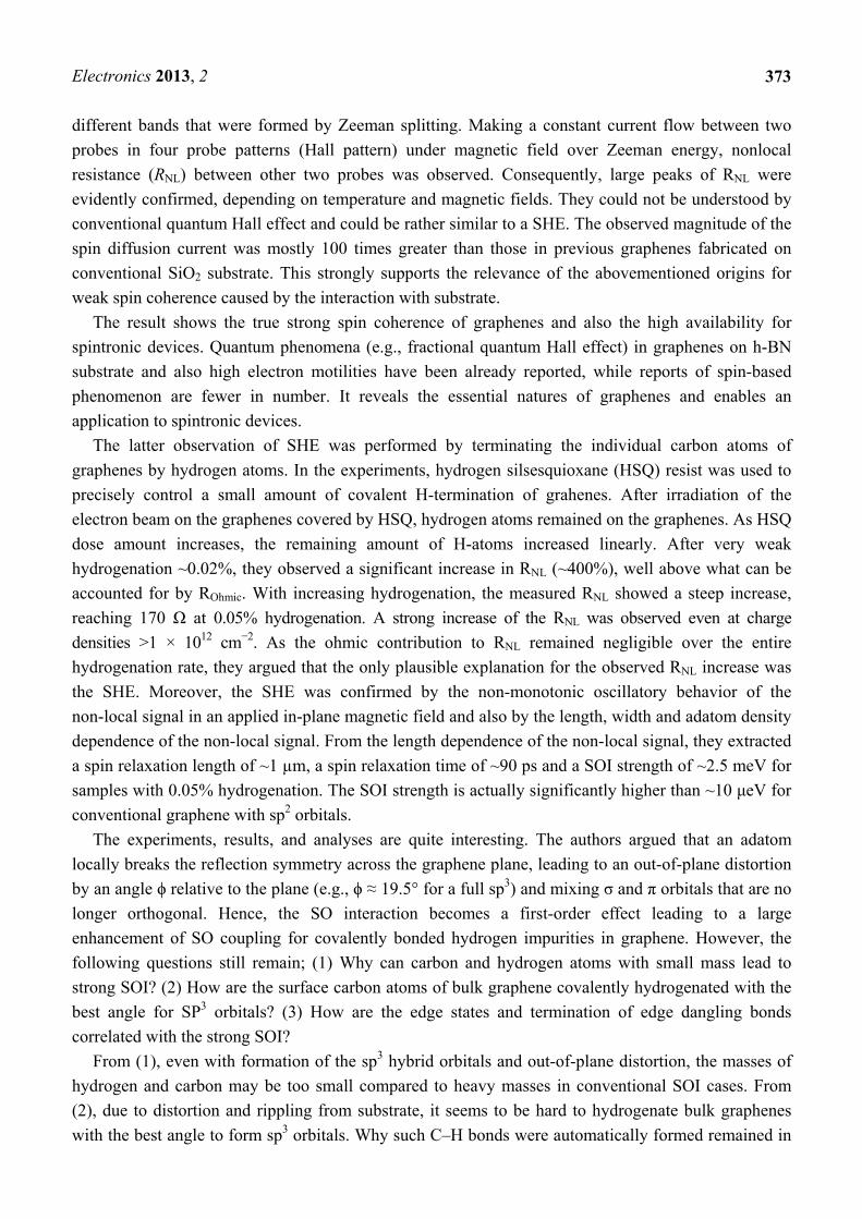
GNMs, which have honeycomb-like array of hexagonal nanopores (Figure 1b,e), were fabricated on
a large ensemble of mechanically exfoliated graphenes (or graphenes CVD-synthesized on SiC
substrate) by using NPAT (Figure 1a) [48] as an etching mask (Figure 1c), following our previous
nonlithographic method [27,36]. The NPAT is easily fabricated through self-organization by anodic
oxidation of pure (99.99%) aluminum films. The graphene was carefully etched by optimized
low-power Ar gas (e.g., 200–600 V for 10–40 min) so as to avoid giving damages (Figure 1d) and the
naomesh of the NPAT was transferred to graphene. Then, the NPAT was detached from the surface of
the fabricated GNM, either mechanically or chemically.
All the GNMs fabricated through these processes (including Figure 2c,f sample) were annealed at
800 C in high vacuum (10−6 Torr) for 0.5–3 days with continual pumping of gas and, then, in
hydrogen gas by the field-emission-type radical CVD system under pressure > 1 MPa at least for 3 h at
for all the measurements. The first annealing is for deoxidization of the pore edges with recovering all
damages and defects and is the key to forming zigzag pore edges by edge atomic reconstruction, while
the second annealing is the key for termination of the carbon atoms at the pore edges by hydrogen atoms.
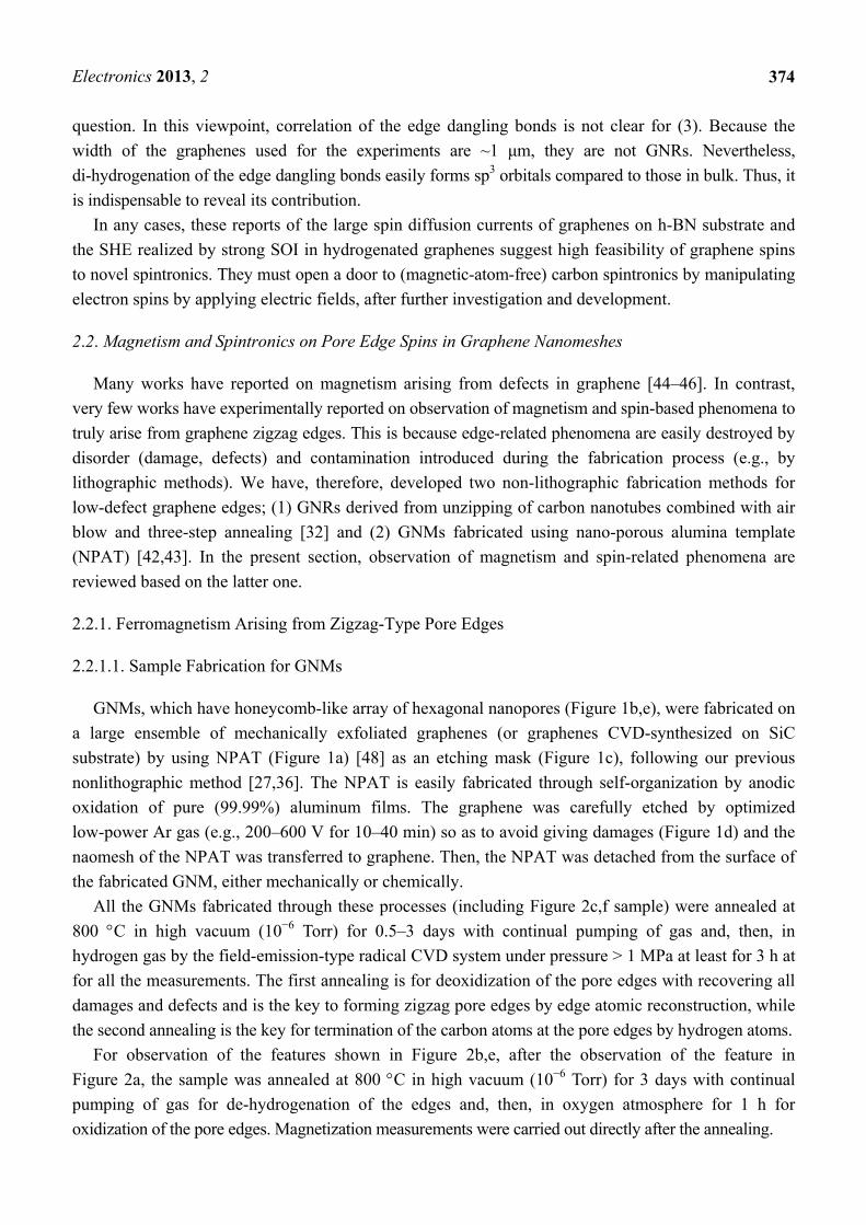
For observation of the features shown in Figure 2b,e, after the observation of the feature in
Figure 2a, the sample was annealed at 800 C in high vacuum (10−6 Torr) for 3 days with continual
pumping of gas for de-hydrogenation of the edges and, then, in oxygen atmosphere for 1 h for
oxidization of the pore edges. Magnetization measurements were carried out directly after the annealing.
Electronics 2013, 2
375
Figure 1. (a) SEM top view of a nano-porous alumina template (NPAT), which shows
honeycomb-like array of hexagonal nano-pores; (b) AFM image of a graphene nanomesh
(GNM) transferred following (c) and (d), which also proves the hexagonal shape of the
pores (mean diameter ϕ ~ 80 nm and mean inter-pore distance W ~ 20 nm);
(c,d) Schematic cross sectional views of nonlithographic fabrication process of a GNM;
(c) NPAT was placed on graphene as an etching mask; (d) The graphene is carefully etched
by Ar gas, resulting in formation of a GNM; (e) Schematic view of a GNM with the
zigzag-type pore-edge. Interpore regions can correspond to GNRs. Actual interpore regions
include a larger number of hexagonal carbon unit cells per inter-pore region with length
~40 nm and W ~ 20 nm. This GNM structure brings at least three large advantages as
mentioned in the text.
Figure 2. Magnetization of monolayer GNMs with ϕ ~ 80 nm and W ~ 20 nm for
termination of different atoms. (a,d) hydrogen-terminated pore edges; (b,e) oxygen-terminated
pore edges; and (c,f) bulk graphene without pore arrays. DC magnetization was measured
by a superconducting quantum interference device (SQUID; Quantum Design). Magnetic
fields were applied perpendicular to GNMs. The vertical axis in panels (a) and (d) denote
magnetic moment per localized-edge π orbital, assuming mono-hydrogenation of individual
edge carbon atoms as explained in text.
Electronics 2013, 2
376
This method brings at least the following three significant benefits. (1) It gives fewer defects and
contamination to the nanopore edges of GNMs because of the non-lithographic method; (2) The
honeycomb-like array of hexagonal nanopores can result in the formation of a large ensemble of GNRs
and pore edges with sufficient lengths (e.g., 40 nm in the present case), because one hexagonal nanopore
can have six edges and the inter-pore regions can correspond to GNRs (Figure 1e). In the actual GNM,
it is speculated that mixture of zigzag and armchair edges exists in one interpore GNR (one pore edge),
as reported by previous STM observation [49]. Even so, a large number of GNRs in the present GNMs
can yield a large area of assembled zigzag-edge GNRs. This is extremely effective in detecting small
magnetic and electric signals arising from the pore edges; (3) When one would align the atomic structure
of one pore edge to zigzag, the other five pore edges can automatically have zigzag atomic structure
from a topological reason. At the current stage, this is impossible and we unintentionally form zigzag
pore edges only via critical-temperature annealing, unlike in [35].
We have no direct evidence for the presence of zigzag-type pore edges. In [42], however, we
indirectly proved presence of zigzag atomic structure at the pore edges by observation of the highly
suppressed ratios of D/G peak heights (<0.2) in Raman spectroscopy, which were realized by
reconstruction of edge atomic structure to zigzag type by the critical-temperature annealing. Indeed, at
least two other groups reported similar correlation previously in intentionally fabricated zigzag-edged
hexagonal nanopores [35] and also graphene flakes [40]. Conventionally, low D/G peak ratios can be
evidence for low defects in samples. In contrast, they can also be evidence for zigzag pore edges when
one dimensionality of the edges is taken into account [40].
As mentioned above, we could not intentionally form zigzag-type pore-edge atomic structure (e.g.,
using the advantage (3) mentioned above). In [30,31], however, it is suggested that the zigzag edge is
the most stable chemically and that arm chair-based edges are reconstructed to zigzag after STM Joule
heating for long edges of overlapped graphenes [30] and electron beam (EB) irradiation for pore
edges [31]. This stability may be simply understood by the difference in the number of carbon atoms
bonded to two neighboring carbon atoms (dangling bonds) for the zigzag edge (i.e., one such atom)
and arm chair edges (two such atoms) [31]. After removal of such atoms, the arm chair edge requires
energy two-times larger than zigzag in order to repair the removed atoms and, thus, becomes unstable.
In our system, we carried out high-temperature annealing for narrow (W ~ 20 nm) GNRs (i.e., narrow
inter-pore spacing). This should bring the energy similar to that in [30,31] and cause the reconstruction
of pore edge atomic structures to zigzag.
Moreover, the observed anomalous periodic-magnetoresistance (MR) oscillation also showed the
presence of localized electrons at the pore edges in H-terminated GNMs [42]. This also supports the
presence of the H-terminated zigzag-type pore edges [42].
2.2.1.2. Magnetism on Pore Edge Termination by Different Foreign Atoms
The results of magnetization measured for different-foreign-atom terminated monolayer GNM are
shown in Figure 2. A ferromagnetic-hysteresis loop with large amplitude is clearly observed only in
H-terminated samples in Figure 2a,d, which showed the low D/G peak ratio values (<0.2). In addition
to this sample, three other samples with low D/G peak heights in Raman spectroscopy exhibited
similar ferromagnetism. In contrast, O-terminated GNMs exhibit a diamagnetism-like weak hysteresis
Electronics 2013, 2
377
loop (Figure 2b,e). This is consistent with [23], which reported that the formation of a spin-paired C–O
chemical bond drastically reduces the local atomic magnetic moment of carbon at the zigzag edge of
GNRs and suppresses the emergence of ferromagnetism.
Bulk graphenes without any pores and those assembled with NPATs show mostly no such features,
even after H2 annealing (Figure 2c,f), implying no contribution of parasitic factors (e.g., defects,
impurities) of bulk graphenes. Moreover, the presence of fewer damages or impurities is reconfirmed
in most the of bulk-graphene regions, because mechanically exfoliated bulk graphenes show an
extremely low D/G peak heights (<<0.1) and a high 2D peak intensity in the Raman spectroscopy.
These results strongly suggest that the observed ferromagnetism is associated with polarized spins
localizing at the H-terminated zigzag-pore edges. It is surprising that the ferromagnetism observed at
2 K appears even at room temperature with a larger magnitude of the hysteresis loops (Figure 2d).
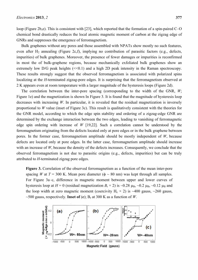
The correlation between the inter-pore spacing (corresponding to the width of the GNR, W;
Figure 1e) and the magnetization is shown In Figure 3. It is found that the magnitude of hysteresis loop
decreases with increasing W. In particular, it is revealed that the residual magnetization is inversely
proportional to W value (inset of Figure 3c). This result is qualitatively consistent with the theories for
the GNR model, according to which the edge spin stability and ordering of a zigzag-edge GNR are
determined by the exchange interaction between the two edges, leading to vanishing of ferromagnetic
edge spin ordering with increase of W [19,22]. Such a correlation cannot be understood by the
ferromagnetism originating from the defects located only at pore edges or in the bulk graphene between
pores. In the former case, ferromagnetism amplitude should be mostly independent of W, because
defects are located only at pore edges. In the latter case, ferromagnetism amplitude should increase
with an increase of W, because the density of the defects increases. Consequently, we conclude that the
observed ferromagnetism is not due to parasitic origins (e.g., defects, impurities) but can be truly
attributed to H-terminated zigzag pore edges.
Figure 3. Correlation of the observed ferromagnetism as a function of the mean inter-pore
spacing W at T = 300 K. Mean pore diameter (ϕ ~ 80 nm) was kept through all samples.
For Figure 3a–c, difference in magnetic moment between upper and lower curves of
hysteresis loop at H = 0 (residual magnetization Br × 2) is ~0.28 μB, ~0.2 μB, ~0.12 μB and
the loop width at zero magnetic moment (coercivity Hc × 2) is ~400 gauss, ~260 gauss,
~500 gauss, respectively. Inset of (c); Br at 300 K as a function of W.
Electronics 2013, 2
378
This is also consistent with MFM observation as shown in Figure 4. It clearly exhibits the presence
of high density of polarized spins at the interpore GNR regions and also edge polarized spins at some
pore edges. Because non-ferromagnetic samples show no such features, the observed ferromagnetism
is attributed to these polarized spins. To date, approximately 50% of the samples, which include
samples showing the low D/G peak heights, have shown ferromagnetism.
Figure 4. Magnetic force microscope (MFM) images of an H-terminated ferromagnetic
GNM on SiC substrate. CoPtCr-coated Si probe was used for the measurements with a
tapping mode. The interpore regions, which correspond to GNRs and exhibit darker color,
imply high density of polarized spins. They directly suggest that the observed ferromagnetism
originates from the GNRs. In particular, two arrows evidently imply the presence of edge
polarized spins.
Disappearance of ferromagnetism in oxygen-terminated GNMs is interpreted as follows. Ref.[6]
reported that the formation of a spin-paired C=O chemical bond drastically reduces the local atomic
magnetic moment of carbon at the zigzag edge of GNRs and suppresses the emergence of
ferromagnetism. The disappearance of ferromagnetism in Figure 2b,e is qualitatively consistent with
this theory.
Moreover, in Figure 2b,e, even the diamagnetism of graphene mostly disappeared. One of the
reasons for this is attributed to the formation of the nanomesh, because such an array drastically
reduces the bulk graphene area available for the presence of loop currents to produce diamagnetism at
the currently applied magnetic-field range (i.e., corresponding to only GNRs with W ~ 20 nm between
nanopores; Figure 1e). The radius of the cyclotron motion for electrons is given by
Rc = (πnS)1/2(h/2π)/eB [42]. By observing the magnetoresistance (i.e., commensurability peak), we
calculate nS to be ~(4 × 10¹¹) cm−2 in the present GNMs. Based on this ns value, Rc is calculated to be
as large as ~400 nm, even for the currently applied largest magnetic field of 1000 gauss in Figure 2.
Indeed, this Rc value is 20 times larger than W ~ 20 nm between the present nanopores, and it prohibits
the emergence of loop currents for the formation of diamagnetism.
2.2.1.3. Theoretical Confirmation by Two Models: GNR Model and Lieb’s Theorem
Here, two theoretical calculations quantitatively support our interpretation mentioned above.
At first, employing the GNR model, which assumes pure zigzag pore edges (i.e., without any defects)
at all regions, enables the estimation of the magnetic moment of edge carbon atoms that contributes to
the ferromagnetism observed in Figure 2. Assuming that only edge dangling bonds have localized spin
Electronics 2013, 2
379
moments, the magnetic moment per edge dangling bond prior to H termination is estimated to be
(1.2 × 10⁻²³)/(μB = 9.3 × 10⁻²⁴) ~1.3 μB, where μB is the Bohr magneton, from the following.
The magnetic moment per edge dangling bond prior to H termination is estimated according to the
following steps; (1) The total area of assembled bulk graphenes used for the pore array formation is
~4 cm2; (2) The area of one hexagonal unit cell with a pore is S = 6(3−1/2/2)(a/2)2 ~ 4300 nm2, where
a = [80 nm (pore diameter) + 20 nm (interpore spacing)]; (3) Thus, the total number of pores is
(4 cm2)/(4300 nm2) ~ 1011 [(1)/(2)]; (4) The total number of dangling bonds per hexagonal pore is
(40 nm)/(0.142 nm × 31/2) × 6 = 166 × 6~1000; (5) The total number of edge dangling bonds of the
GNM used for the SQUID measurement is 1014 [(3) × (4)].
Therefore, using (5), the saturation magnetization per edge dangling bond is estimated to be
1.2 × 10⁻⁶ (emu) × 10−3/1014 = 1.2 × 10⁻²³ (J/T). Thus, the magnetic moment per edge dangling bond is
estimated to be (1.2 × 10⁻²³)/(μB = 9.3 × 10⁻²⁴) ~1.3 μB, where μB is the Bohr magneton. Conventionally,
GNRs with no H-termination of dangling bonds should show antiferromagnetism, theoretically.
However, in the above estimation, the observed total magnetization was divided by estimated number
of edge dangling bonds in the GNM, leading us to neglect this theory.
Next, after H annealing at critical temperature, edge dangling bonds of a GNR are terminated by H
atoms [3,5–7,9]. The following three types of H terminations are theoretically possible. (1) All edge
dangling bonds are each terminated by one H atom on the side of both zigzag edges. It provides a flat
band for 2π/3 ≤ k ≤ π in the Brillouin zone. Electrons are well localized at the edges; (2) Each of the
edge dangling bonds on one side are terminated by two H atoms (so that the edge carbon atom
becomes tetrahedrally coordinated; a bearded edge), while the dangling bonds on the opposite side are
terminated by a single H atom. The GNR provides a flat band for 0 ≤ k ≤ π, resulting in a completely
localized “on-bonding state” around the Fermi level (EF). This leads to the spin polarization of all
carbon atoms; (3) The double H atom termination of the zigzag-edge carbon atoms on both sides of a
GNR provides a flat band for 0 ≤ k ≤ 2π/3 and creates a modified zigzag edge.
The type of edge H-termination could not be observed in the present experiment. However, our case
should correspond to case (1) from the following reason. The mono-H termination of the edge
dangling bond decreases its magnetic moment to one μB. The magnetic moment of one localized-edge
π orbital is, therefore, estimated to be as large as (~1.3 μB–1 μB) = ~0.3 μB. This is in fairly good
agreement with the theoretical contribution of the π-orbital state to the edge magnetic moment of
~0.3 μB in a zigzag-edged GNR within the ferromagnetically ordered spin configuration [22].
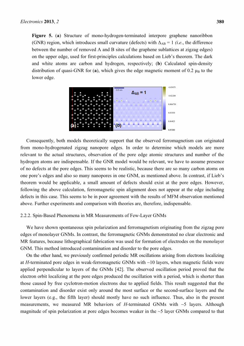
As for the other model, we employ Lieb’s model [39], which predicts the appearance of net
magnetization arising from small defects in sublattice of carbon hexagonal cell (i.e., missing A and B
sites underlying bipartite lattice). Even a small defect may still remain in actual pore edges. In order to
elucidate the influence of such residual small-volume edge disorder on magnetism of GNM, we
performed systematic first-principles calculations of magnetic properties of quasi-GNR structures
(Figure 5a, corresponding to the inter-pore region) based on Lieb’s theorem [50], which introduces the
slight disorder at the upper edge. Interestingly, the ground state of quasi-GNR structure turned out to be
ferromagnetic in Figure 5b. The calculated net magnetic moment follows Lieb’s theorem with local
moments up to 0.2 μB/edge atom and depends on magnitude of the assumed edge disorder. These
values agree fairly well with the value estimated from the GNR model.
Electronics 2013, 2
380
Figure 5. (a) Structure of mono-hydrogen-terminated interpore graphene nanoribbon
(GNR) region, which introduces small curvature (defects) with ΔAB = 1 (i.e., the difference
between the number of removed A and B sites of the graphene sublattices at zigzag edges)
on the upper edge, used for first-principles calculations based on Lieb’s theorem. The dark
and white atoms are carbon and hydrogen, respectively; (b) Calculated spin-density
distribution of quasi-GNR for (a), which gives the edge magnetic moment of 0.2 μB to the
lower edge.
Consequently, both models theoretically support that the observed ferromagnetism can originated
from mono-hydrogenated zigzag nanopore edges. In order to determine which models are more
relevant to the actual structures, observation of the pore edge atomic structures and number of the
hydrogen atoms are indispensable. If the GNR model would be relevant, we have to assume presence
of no defects at the pore edges. This seems to be realistic, because there are so many carbon atoms on
one pore’s edges and also so many nanopores in one GNM, as mentioned above. In contrast, if Lieb’s
theorem would be applicable, a small amount of defects should exist at the pore edges. However,
following the above calculation, ferromagnetic spin alignment does not appear at the edge including
defects in this case. This seems to be in poor agreement with the results of MFM observation mentioned
above. Further experiments and comparison with theories are, therefore, indispensable.
2.2.2. Spin-Based Phenomena in MR Measurements of Few-Layer GNMs
We have shown spontaneous spin polarization and ferromagnetism originating from the zigzag pore
edges of monolayer GNMs. In contrast, the ferromagnetic GNMs demonstrated no clear electronic and
MR features, because lithographical fabrication was used for formation of electrodes on the monolayer
GNM. This method introduced contamination and disorder to the pore edges.
On the other hand, we previously confirmed periodic MR oscillations arising from electrons localizing
at H-terminated pore edges in weak-ferromagnetic GNMs with ~10 layers, when magnetic fields were
applied perpendicular to layers of the GNMs [42]. The observed oscillation period proved that the
electron orbit localizing at the pore edges produced the oscillation with a period, which is shorter than
those caused by free cyclotron-motion electrons due to applied fields. This result suggested that the
contamination and disorder exist only around the most surface or the second-surface layers and the
lower layers (e.g., the fifth layer) should mostly have no such influence. Thus, also in the present
measurements, we measured MR behaviors of H-terminated GNMs with ~5 layers. Although
magnitude of spin polarization at pore edges becomes weaker in the ~5 layer GNMs compared to that
Electronics 2013, 2
381
of monolayer GNMs, we confirmed that the GNMs actually exhibited evident ferromagnetism in
magnetization measurement and proved presence of polarized edge spins [38].
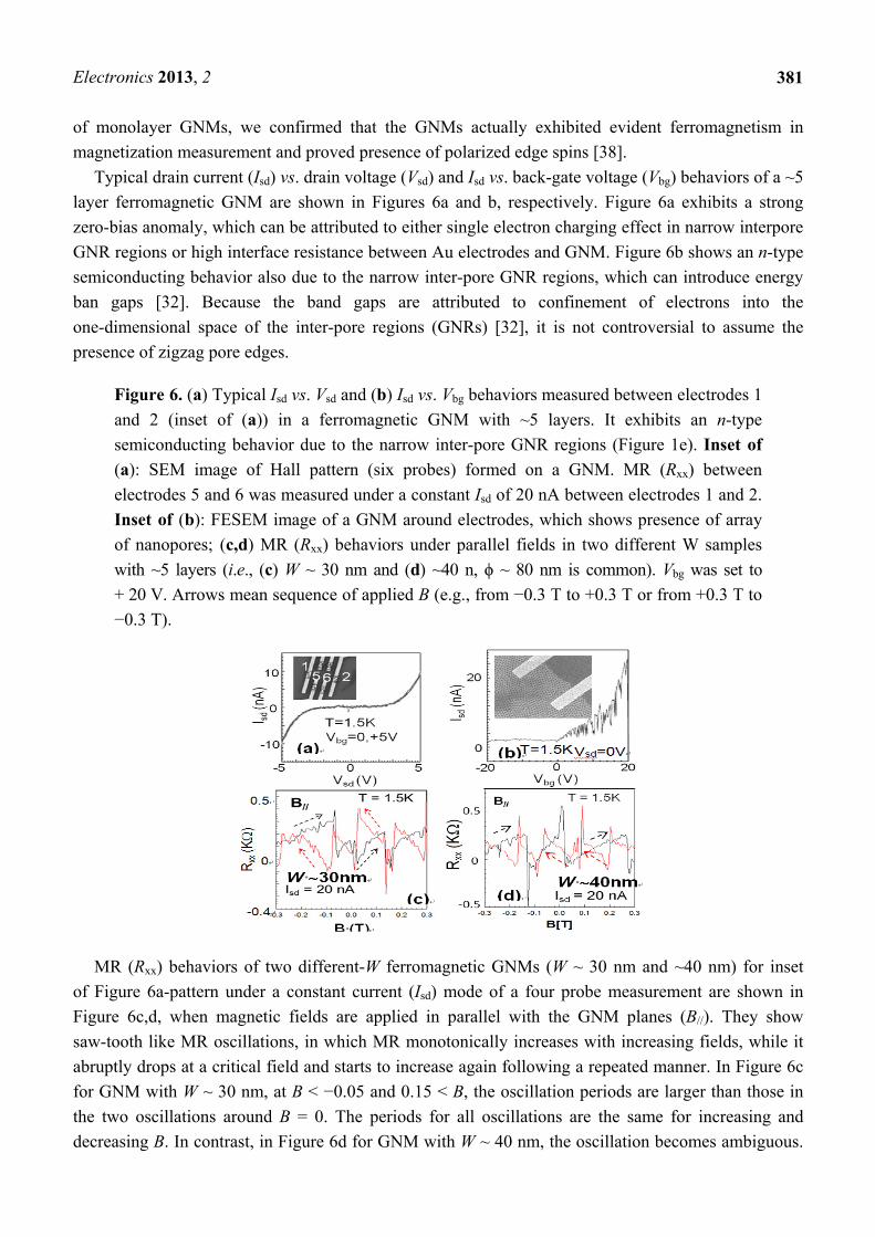
Typical drain current (Isd) vs. drain voltage (Vsd) and Isd vs. back-gate voltage (Vbg) behaviors of a ~5
layer ferromagnetic GNM are shown in Figures 6a and b, respectively. Figure 6a exhibits a strong
zero-bias anomaly, which can be attributed to either single electron charging effect in narrow interpore
GNR regions or high interface resistance between Au electrodes and GNM. Figure 6b shows an n-type
semiconducting behavior also due to the narrow inter-pore GNR regions, which can introduce energy
ban gaps [32]. Because the band gaps are attributed to confinement of electrons into the
one-dimensional space of the inter-pore regions (GNRs) [32], it is not controversial to assume the
presence of zigzag pore edges.
Figure 6. (a) Typical Isd vs. Vsd and (b) Isd vs. Vbg behaviors measured between electrodes 1
and 2 (inset of (a)) in a ferromagnetic GNM with ~5 layers. It exhibits an n-type
semiconducting behavior due to the narrow inter-pore GNR regions (Figure 1e). Inset of
(a): SEM image of Hall pattern (six probes) formed on a GNM. MR (Rxx) between
electrodes 5 and 6 was measured under a constant Isd of 20 nA between electrodes 1 and 2.
Inset of (b): FESEM image of a GNM around electrodes, which shows presence of array
of nanopores; (c,d) MR (Rxx) behaviors under parallel fields in two different W samples
with ~5 layers (i.e., (c) W ~ 30 nm and (d) ~40 n, ϕ ~ 80 nm is common). Vbg was set to
+ 20 V. Arrows mean sequence of applied B (e.g., from −0.3 T to +0.3 T or from +0.3 T to
−0.3 T).
MR (Rxx) behaviors of two different-W ferromagnetic GNMs (W ~ 30 nm and ~40 nm) for inset
of Figure 6a-pattern under a constant current (Isd) mode of a four probe measurement are shown in
Figure 6c,d, when magnetic fields are applied in parallel with the GNM planes (B//). They show
saw-tooth like MR oscillations, in which MR monotonically increases with increasing fields, while it
abruptly drops at a critical field and starts to increase again following a repeated manner. In Figure 6c
for GNM with W ~ 30 nm, at B < −0.05 and 0.15 < B, the oscillation periods are larger than those in
the two oscillations around B = 0. The periods for all oscillations are the same for increasing and
decreasing B. In contrast, in Figure 6d for GNM with W ~ 40 nm, the oscillation becomes ambiguous.
Electronics 2013, 2
382
We call this saw-tooth like MR oscillation the spin pumping effect. The effect means a repeated cycle
of gradual accumulation (increased number) of polarized spins and its abrupt emission (decreased
number) at critical fields. No such anomalous behavior can be reported in any previous MR
phenomena (e.g., ferromagnetic MR behavior, giant MR, tunnel MR, and spin valve effect), which is
mentioned in the introduction.
In the present case, spin-polarized electrons localize at the pore edges under thermal equilibrium.
However, under non thermal equilibrium caused by a constant current flow, the flat bands at the
pore edges are modulated. Thus, some of the polarized electron-spins can no longer localize at the
pore edges and flow through interpore bulk graphene regions. In our previous ~10-layer GNMs with
W ~ 20 nm [42], the spin pumping effect was not observed even under parallel fields, although MR
oscillation arising from pore-edge localized electrons was found under perpendicular fields. This
implies that enough inter-pore space W with bulk grapheme regions for electron transport is
indispensable for the spin flow and detection of the spin pumping effect.
Qualitatively possible interpretation for the present spin pumping effect is explained as follows.
When the applied magnetic field is increased, the number of the localized polarized-spins increases at
the pore edges. Moreover, other free electrons, which are flowing through bulk graphene regions
among the pores, also tend to accumulate and polarize, when they locate close to the flat energy band
of the pore edges. However, the accumulation of polarized-spins saturate at the pore edges. Then, the
excess spins are abruptly emitted at a critical field, as parallel magnetic fields increase further, because
the flat band is modulated in the GNM plane by increasing parallel fields more or less. After the
emission of the accumulated excess spins, the flat band partially recovers near to the initial condition
and the pore edges can allow the accumulation of further spins. Then, the MR starts to increase again,
resulting in a repeated saw-tooth like feature. In Figure 6d for the GNM with W ~ 40 nm, the
saw-tooth like oscillation becomes ambiguous, as mentioned above. This is qualitatively consistent
with a decrease in ferromagnetism amplitude shown in Figure 3c, that is, reduction of amplitude of
polarized spins at the pore edges in monolayer GNMs. This suggests the presence of optimized W
values (e.g., 30 nm), which is the most suitable for appearance of spin pumping effect, with respect to
the amount of pore edge polarized spins and its flow through array of nanopores.
The large W values induce spin flow through the interpore GNR regions, while it weakens magnitude
of the polarized spins at the pore edges. In contrast, the small W values induce the amount of the
polarized spins at the pore edges. It also obstructs sufficient spin flow via the interpore regions
between electrodes and makes the detection of the spin flow difficult. Further optimization of the
structures and clarifying the exact mechanism, therefore, are expected in the near future.
3. Conclusions
Recent advancement of the spin-based research of graphenes and our experiments for the
edge-based spin phenomena have been reviewed. The former promises precise manipulation of
coherent spins by applying electric fields. Avoiding the negative influence of substrate-based factors is
crucial (e.g., by using h-BN substrate). In the latter, we successfully fabricated low-defected
mono-layer GNMs by using a non-lithographic method (i.e., using NPATs) and found the spontaneous
emergence of large-amplitude ferromagnetism, only when pore edges of the GNMs were
Electronics 2013, 2
383
H-terminated. Observed correlation between the inter-pore spacing and magnetism supported that it
was attributed to electrons localizing at the zigzag pore-edges, which was in quantitative agreement
with theories for pure GNR and defected-GNR models (Lieb’s theorem). Moreover, the spin pumping
effect was observed for fields applied in parallel with the GNM planes in few-layer GNMs with the
optimized inter-pore spacing (~30 nm).
All-carbon spintronics is the key factor to realize magnetic rare-element free spintronic devices,
which overcome the present material resource and environmental contamination problems. Strong spin
coherence and its polarized edge spins of graphene must open the door to the novel spintronics with
invisible, flexible, and ultra-light (wearable) features.
Acknowledgments
The author thank H. Yang and M. Chshiev for the first principle calculation, K. Fujita, Y.
Hashimoto, E. Endo, Y. Iye, S. Katsumoto, M. Yamamoto, S. Tarucha for the device fabrication
processes, T. Ando, T. Enoki, M. Koshino, J. Akimitsu, T. Muranaka, H.Aoki, S. Roche, X. Jia, and
M. S. Dresselhaus for their fruitful discussions and encouragement. This work at Aoyama Gakuin was
partly supported by a Grant-in-aid for Scientific Research (Basic research A: 24241046) in MEXT, a
High-Technology Research Center Project for private universities in MEXT, and also AFOSR grant.
Conflicts of Interest
The authors declare no conflict of interest.
References
1. Baibich, M.N.; Broto, J.M.; Fert, A.; Van Dau, F.N.; Petroff, F.; Etienne, P.; Creuzet, G.;
Friederich, A.; Chazelas, J. Giant magnetoresistance of (001)Fe/(001)Cr magnetic superlattices.
Phys. Rev. Lett. 1988, 61, 2472.
2. Moodera, J.S.; Kinder, L.R.; Wong, T.M.; Meservey, R. Large magnetoresistance at room
temperature in ferromagnetic thin film tunnel junctions. Phys. Rev. Lett. 1995, 74, 3273–3276.
3. Yuasa, S.; Nagahama, T.; Fukushima, A.; Suzuki, Y.; Ando, K. Giant room-temperature
magnetoresistance in single-crystal Fe/MgO/Fe magnetic tunnel junctions. Nat. Mat. 2004, 3,
868–871.
4. Hayakawa, J.; Ikeda, S.; Lee, Y.M.; Matsukura, F.; Ohno, H. Effect of high annealing temperature
on giant tunnel magnetoresistance ratio of magnetic tunnel junctions. Appl. Phys. Lett. 2006,
89, 232510.
5. Munekata, H.; Ohno, H.; von Molnar, S.; Segmüller, A.; Chang, L.L.; Esaki, L. Diluted magnetic
III-V semiconductors, Phys. Rev. Lett. 1989, 63, 1849–1852.
6. Ohno, H.; Munekata, H.; Penney, T.; von Molnár, S.; Chang, L.L. Magnetotransport properties of
p-type (In,Mn)As diluted magnetic III-V semiconductors. Phys. Rev. Lett. 1992, 68, 2664–2667.
7. Hai, P.N.; Ohya, S.; Tanaka, M.; Barnes, S.E.; Maekawa, S. Electromotive force and huge
magnetoresistance in magnetic tunnel junctions. Nature 2009, 458, 489–492.
Electronics 2013, 2
384
8. Lundeberg, M.B.; Yang, R.; Renard, J.; Folk, J.A. Defect-mediated spin relaxation and dephasing
in graphene. Phys. Rev. Lett. 2013, 110, 156601.
9. Sun, Z.; Raji, A.O.; Zhu, Y.; Xiang, C.; Yan, Z.; Kittrell, C.; Samuel, E.L.G.; Tour, J.M.
Large-area Bernal-stacked bi-, tri-, and tetralayer grapheme. Nano 2012, 6, 7615.
10. Tombros, N.; Jozsa, C.; Popinciuc, M.; Jonkman, H.T.; Van Wees, B.J. Electronic spin transport
and spin precession in single graphene layers at room temperature. Nature 2007, 448, 571–574.
11. Tombros, N.; Tanabe, S.; Veligura, A.; Jozsa, C.; Popinciuc, M.; Jonkman, H.T.; Van Wees, B.J.
Anisotropic spin relaxation in graphene. Phys. Rev. Lett. 2008, 101, 046601.
12. Abanin, D.A.; Morozov, S.V.; Ponomarenko, L.A.; Gorbachev, R.V.; Mayorov, A.S.;
Katsnelson, M.I.; Watanabe, K.; Taniguchi, T.; Novoselov, K.S.; Levitov, L.S. Giant nonlocality
near the Dirac point in graphene. Science 2011, 332, 328–330.
13. Murakami, S.; Nagaosa, N.; Zhang, S. Dissipationless quantum spin current at room temperature.
Science 2003, 301, 1348–1351.
14. Kane, C.L.; Mele, E.J. Quantum spin hall effect in graphene. Phys. Rev. Lett. 2005, 95,
226801–226804.
15. Kane, C.L. Graphene and the quantum spin hall effect. J. Mod. Phys. B 2007, 21, 1155.
16. Schmidt, M.J.; Loss, D. Edge states and enhanced spin-orbit interaction at graphene/graphane
interfaces. Phys. Rev. B 2010, 81, 165439.
17. Balakrishnan, J.; Koon, G.K.W.; Jaiswal, M.; Neto, A.H.C.; Özyilmaz, B. Colossal enhancement of
spin-orbit coupling in weakly hydrogenated graphene. Nat. Phys. 2013, 9, 284–287.
18. Nakada, K.; Fujita, M.; Dresselhaus, G.; Dresselhaus, M.S. Edge state in graphene ribbons:
Nanometer size effect and edge shape depend. Phys. Rev. B 1996, 54, 17954–17961.
19. Fujita, M.; Wakabayashi, K.; Nakada, K.; Kusakabe, K. Peculiar localized state at zigzag graphite
edge. J. Phys. Soc. Jpn. 1996, 65, 1920–1923.
20. Kusakabe, K.; Maruyama, M. Magnetic nanographite. Phys. Rev. B 2003, 67, 092406.
21. Okada, S.; Oshiyama, A. Magnetic Ordering in Hexagonally Bonded Sheets with First-Row
Elements. Phys. Rev. Lett. 2001, 87, 146803.
22. Lee, H.; Son, Y.; Park, N.; Han, S.; Yu, J. Magnetic ordering at the edges of graphitic fragments:
Magnetic tail interactions between the edge-localized states. Phys. Rev. B 2005, 72, 174431.
23. Veiga, R.G.A.; Miwa, R.H.; Srivastava, G.P. Quenching of local magnetic moment in oxygen
adsorbed graphene nanoribbons. J. Chem. Phys. 2008, 128, 201101.
24. Lee, H.; Park, N.; Son, Y.; Han, S.; Yu, J. Ferromagnetism at the edges of the stacked graphitic
fragments: An ab initio study. Chem. Phys. Lett. 2004, 398, 207–211.
25. Enoki, T.; Takai, K. The edge state of nanographene and the magnetism of the edge-state spins.
Sol. Stat. Comm. 2009, 149, 1144–1150.
26. Son, Y.; Cohen, M.L.; Louie, S.G. Energy gaps in graphene nanoribbons. Phys. Rev. Lett. 2006,
97, 216803.
27. Yang, L.; Park, C.; Son, Y.; Cohen, M.L.; Louie, S.G. Quasiparticle energies and band gaps in
graphene nanoribbons. Phys. Rev. Lett. 2007, 99, 186801.
28. Shima, N.; Aoki, H. Electronic structure of super-honeycomb systems: A peculiar realization of
semimetal/semiconductor classes and ferromagnetism. Phys. Rev. Lett. 1993, 71, 4389–4392.

Electronics 2013, 2
385
29. Rosser, J.F.; Palacios, J.J. Magnetism in Graphene Nanoislands. Phys. Rev. Lett. 2007,
99, 177204.
30. Jia, X.; Hofmann, M.; Meunier, V.; Sumpter, B.G.; Campos-Delgado, J.; Romo-Herrera, J.M.;
Son, H.; Hsieh, Y.; Reina, A.; Kong, J. Controlled formation of sharp zigzag and armchair edges
in graphitic nanoribbons. Science 2009, 323, 1701–1705.
31. Girit, Ç.Ö.; Meyer, J.C.; Erni, R.; Rossell, M.D.; Kisielowski, C.; Yang, L.; Park, C.;
Crommie, M.F.; Cohen, M.L.; Louie, S.G. Graphene at the edge: Stability and dynamics. Science
2009, 323, 1705–1708.
32. Shimizu, T.; Haruyama, J.; Marcano, D.C.; Kosinkin, D.V.; Tour, J.M.; Hirose, K.; Suenaga, K.
Large intrinsic energy bandgaps in annealed nanotube-derived graphene nanoribbons. Nat.
Nanotech. 2011, 6, 45–50.
33. Han, M.Y.; Brant, J.C.; Kim, P. Electron transport in disordered graphene nanoribbons. Phys. Rev.
Lett. 2010, 104, 056801.
34. Wang, X.; Ouyang, Y.; Li, X.; Wang, H.; Guo, J.; Dai, H. Room-temperature all-semiconducting
sub-10-nm graphene nanoribbon field-effect transistors. Phys. Rev. Lett. 2008, 100, 206803.
35. Krauss, B.; Nemes-Incze, P.; Skakalova, V.; Biro, L.P.; von Klitzing, K.; Smet, J.H. Raman
scattering at pure graphene zigzag edges. Nano Lett. 2010, 10, 4544–4548.
36. Bai, J.; Zhong, X.; Jiang, S.; Huang, Y.; Duan, X. Graphene nanomesh. Nat. Nanotech. 2010, 5,
190–194.
37. Son, Y.W.; Cohen, M.L.; Louie, S.G. Half-metallic graphene nanoribbons. Nature 2006, 444,
347–349.
38. Otani, M.; Koshino, M.; Takagi, Y.; Okada, S. Intrinsic magnetic moment on (0001) surfaces of
rhombohedral graphitee. Phys. Rev. B 2010, 81, 161403 (R).
39. Yang, H.; Chshiev, M.; Boukhvalov, D.W.; Waintal, X.; Roche, S. Inducing and optimizing
magnetism in graphene nanomeshes. Phys. Rev. B 2011, 84, 214404.
40. You, Y.M.; Ni, Z.H.; Yu, T.; Shen, Z.X. Edge chirality determination of graphene by Raman
spectroscopy. Appl. Phys. Lett. 2008, 93, 163112.
41. Soriano, D.; Leconte, N.; Ordejón, P.; Charlier, J.; Palacios, J.; Roche, S. Magnetoresistance and
magnetic ordering fingerprints in hydrogenated graphene. Phys. Rev. Lett. 2011, 107, 016602.
42. Shimizu, T.; Nakamura, J.; Tada, K.; Yagi, Y.; Haruyama, J. Magnetoresistance oscillations
arising from edge-localized electrons in low-defect graphene antidot-lattices. Appl. Phys. Lett.
2012, 100, 023104.
43. Tada, K.; Hashimoto, T.; Haruyama, J.; Yang, H.; Chshiev, M. Spontaneous spin polarization and
spin pumping effect on edges of graphene antidot lattices. Phys. Status Solidi 2012, 249,
2491–2496.
44. Ning, G.; Xu, C.; Hao, L.; Kazakova, O.; Fan, Z.; Wang, H.; Wang, K.; Gao, J.; Qian, W.; Wei, F.
Ferromagnetism in nanomesh graphene . Carbon 2013, 51, 390–396.
45. Nair, R.R.; Sepioni, M.; Tsai, I.; Lehtinen, O.; Keinonen, J.; Krasheninnikov, A.V.; Thomson, T.;
Geim, A.K.; Grigorieva, I.V. Spin-half paramagnetism in graphene induced by point defects. Nat.
Phys. 2012, 8, 199–202.
Electronics 2013, 2
386
46. Rao, S.S.; Jammalamadaka, S.N.; Stesmans, A.; Moshchalkov, V.V.; Van Tol, J.;
Kosynkin, D.V.; Higginbotham-Duque, A.; Tour, J.M. Ferromagnetism in graphene nanoribbons:
Split versus oxidative unzipped ribbons. Nano Lett. 2012, 12, 1210–1217.
47. Prével, B.; Benoit, J.-M.; Bardotti, L.; Mélinon, P.; Ouerghi, A.; Lucot, D.; Bourhis, E.; Gierak, J.
Nanostructuring graphene on SiC by focused ion beam: Effect of the ion fluence. Appl. Phys. Lett.
2011, 98, 83116.
48. Takesue, I.; Haruyama, J.; Kobayashi, N.; Chiashi, S.; Maruyama, S.; Sugai, T.; Shinohara, H.
Superconductivity in entirely end-bonded multiwalled carbon nanotubes. Phys. Rev. Lett. 2006,
96, 057001.
49. Niimi, Y.; Matsui, T.; Kambara, H.; Tagami, K.; Tsukada, M.; Fukuyama, H. Scanning tunneling
microscopy and spectroscopy of the electronic local density of states of graphite surfaces near
monoatomic step edges. Phys. Rev. B 2006, 73, 085421.
50. Asano, H.; Muraki, S.; Endo, H.; Bandow, S.; Iijima, S. Strong magnetism observed in carbon
nanoparticles produced by the laser vaporization of a carbon pellet in hydrogen-containing Ar
balance gas. J. Phys. 2010, 22, 334209.
© 2013 by the authors; licensee MDPI, Basel, Switzerland. This article is an open access article
distributed under the terms and conditions of the Creative Commons Attribution license
(http://creativecommons.org/licenses/by/3.0/).