Graphene-based mid-infrared room-temperature pyroelectric ...
10
ARTICLE Received 9 Sep 2016 | Accepted 16 Dec 2016 | Published 31 Jan 2017 Graphene-based mid-infrared room-temperature pyroelectric bolometers with ultrahigh temperature coefficient of resistance U. Sassi 1 , R. Parret 2 , S. Nanot 2 , M. Bruna 3,w , S. Borini 3,w , D. De Fazio 1 , Z. Zhao 1 , E. Lidorikis 4 , F.H.L. Koppens 2,5 , A.C. Ferrari 1 & A. Colli 6 There is a growing number of applications demanding highly sensitive photodetectors in the mid-infrared. Thermal photodetectors, such as bolometers, have emerged as the technology of choice, because they do not need cooling. The performance of a bolometer is linked to its temperature coefficient of resistance (TCR, B2–4% K 1 for state-of-the-art materials). Graphene is ideally suited for optoelectronic applications, with a variety of reported photo- detectors ranging from visible to THz frequencies. For the mid-infrared, graphene-based detectors with TCRs B4–11% K 1 have been demonstrated. Here we present an uncooled, mid-infrared photodetector, where the pyroelectric response of a LiNbO 3 crystal is trans- duced with high gain (up to 200) into resistivity modulation for graphene. This is achieved by fabricating a floating metallic structure that concentrates the pyroelectric charge on the top-gate capacitor of the graphene channel, leading to TCRs up to 900% K 1 , and the ability to resolve temperature variations down to 15 mK. DOI: 10.1038/ncomms14311 OPEN 1 Cambridge Graphene Centre, University of Cambridge, Cambridge CB3 0FA, UK. 2 ICFO Institut de Ciencies Fotoniques, The Barcelona Institute of Science and Technology, 08860 Castelldefels, Barcelona, Spain. 3 Nokia Technologies, Broers Building, Cambridge CB3 0FA, UK. 4 Department of Materials Science and Engineering, University of Ioannina, Ioannina 45110, Greece. 5 ICREA Institucio ´ Catalana de Recerc ¸a i Estudis Avancats, Barcelona 08010, Spain. 6 Emberion Ltd, Sheraton House, Castle Park, Cambridge CB3 0AX, UK. w Present addresses: Nokia Bell Labs, Broers Building, Cambridge CB3 0FA, UK (M.B.); Graphitene Ltd, SBC Open Innovation Campus, Stevenage, Herts SG1 2FX, UK (S.B.). Correspondence and requests for materials should be addressed to A.C. (email: [email protected]). NATURE COMMUNICATIONS | 8:14311 | DOI: 10.1038/ncomms14311 | www.nature.com/naturecommunications 1
-
Upload
khangminh22 -
Category
Documents
-
view
0 -
download
0
Transcript of Graphene-based mid-infrared room-temperature pyroelectric ...
ARTICLE
Received 9 Sep 2016 | Accepted 16 Dec 2016 | Published 31 Jan 2017
Graphene-based mid-infrared room-temperaturepyroelectric bolometers with ultrahigh temperaturecoefficient of resistanceU. Sassi1, R. Parret2, S. Nanot2, M. Bruna3,w, S. Borini3,w, D. De Fazio1, Z. Zhao1, E. Lidorikis4, F.H.L. Koppens2,5,
A.C. Ferrari1 & A. Colli6
There is a growing number of applications demanding highly sensitive photodetectors in the
mid-infrared. Thermal photodetectors, such as bolometers, have emerged as the technology
of choice, because they do not need cooling. The performance of a bolometer is linked to its
temperature coefficient of resistance (TCR, B2–4%K� 1 for state-of-the-art materials).
Graphene is ideally suited for optoelectronic applications, with a variety of reported photo-
detectors ranging from visible to THz frequencies. For the mid-infrared, graphene-based
detectors with TCRs B4–11%K� 1 have been demonstrated. Here we present an uncooled,
mid-infrared photodetector, where the pyroelectric response of a LiNbO3 crystal is trans-
duced with high gain (up to 200) into resistivity modulation for graphene. This is achieved by
fabricating a floating metallic structure that concentrates the pyroelectric charge on the
top-gate capacitor of the graphene channel, leading to TCRs up to 900%K� 1, and the ability
to resolve temperature variations down to 15 mK.
DOI: 10.1038/ncomms14311 OPEN
1 Cambridge Graphene Centre, University of Cambridge, Cambridge CB3 0FA, UK. 2 ICFO Institut de Ciencies Fotoniques, The Barcelona Institute of Scienceand Technology, 08860 Castelldefels, Barcelona, Spain. 3 Nokia Technologies, Broers Building, Cambridge CB3 0FA, UK. 4 Department of Materials Scienceand Engineering, University of Ioannina, Ioannina 45110, Greece. 5 ICREA Institucio Catalana de Recerca i Estudis Avancats, Barcelona 08010, Spain.6 Emberion Ltd, Sheraton House, Castle Park, Cambridge CB3 0AX, UK. w Present addresses: Nokia Bell Labs, Broers Building, Cambridge CB3 0FA, UK (M.B.);Graphitene Ltd, SBC Open Innovation Campus, Stevenage, Herts SG1 2FX, UK (S.B.). Correspondence and requests for materials should be addressed to A.C.(email: [email protected]).
NATURE COMMUNICATIONS | 8:14311 | DOI: 10.1038/ncomms14311 | www.nature.com/naturecommunications 1
Detecting thermal infrared (IR) radiation of room tem-perature (RT) objects (with spectral peak emittanceB10 mm (refs 1,2)) is increasingly important for
applications in astronomy3, healthcare4,5, smart energysystems6, security7, pollution monitoring8, fire sensing9,automotive10 and motion tracking11. In this spectral region,thermal photodetectors (PDs) that can operate at RT with noneed for cooling are highly desirable2,12.
Pyroelectric detectors are low-cost, uncooled thermal PDs forthe mid-infrared (MIR)1,2,12. They are capacitor-like structureswhere a pyroelectric crystal is sandwiched between two metalelectrodes2. Pyroelectric crystals are materials with a T-dependentspontaneous polarization, P (Cm� 2), i.e., surface densityof bound charge12. Around RT, a linear relation links the Tvariation, DT, with the changes of P1,2,12:
DP¼p � DT ð1Þwhere p (mCm� 2 K� 1) is the pyroelectric coefficient (for thecrystallographic direction perpendicular to the electrodes).The two metal electrodes are connected through an externalload resistor RL. At thermal equilibrium (dT/dt¼ 0), no currentflows in the external circuit, because P is constant and thecharges on the electrodes compensate the bound charges at thepyroelectric surface12. However, when the detector is illuminated,the absorbed radiation heats the crystal and P changes accordingto equation (1)12. The variation of the bound charge surfacedensity will induce a current Ip in the external circuit12:
Ip¼A � dPdt
¼A � p � dTdt
ð2Þ
where A (m2) is the electrode area1,13. Ip flows only as long asT changes (i.e., when the impinging optical power changes).
Bolometers are another class of uncooled thermal PDs, whereT variations due to incoming photons produce a change in theresistance (R) of a sensing element. This can be a thin metallayer14, a semiconductor15 or a superconductor1. Commonmetallic bolometers for RT operation are made of Ti16, Ni17 orPt14. Polysilicon1,2, amorphous silicon18 or vanadium oxide15 areusually exploited for semiconducting bolometers. For fixed bias,Vd, the resistance change of the sensing element translates ina measurable change in current (I). The temperature coefficient ofresistance (TCR in units of %K� 1) is a key performanceindicator for a bolometer and is defined as2:
TCR R0ð Þ¼ 1R0
� dRdT
¼� 1I0� dIdT
ð3Þ
The TCR represents the percentage change in resistance perKelvin around the operating point R0 and corresponds in moduleto the normalized current change per Kelvin around theoperating current I0 (Equation 3). The TCR in metallicbolometers is B0.4%K� 1 (ref. 2), whereas for semiconductingbolometers it is B2–4%K� 1 (refs 1,2). It follows that the outputof a bolometer (measured current) is proportional to T, incontrast to the output of a pyroelectric detector (measuredcurrent) that depends on the derivative of T, see equation (2)13.However, although the TCR of a bolometer does not dependon the device area, in pyroelectric detectors the output current isa function of the electrode size, as for equation (2)13. Largerelectrodes allow the collection of more charge, increasing thepyroelectric current, therefore leading to a larger signal.
These differences have an impact on the suitability of bothtechnologies for different applications. As pyroelectric detectorsare alternating current devices that rely on a variable impingingradiation, they require a chopper at 25–60Hz12 to detectstationary objects and are thus preferentially used to detectmoving targets (e.g., for automatic lighting systems6, electrical
outlet turn-off11, unusual behaviour detection19, home invasionprevention12 and so on), where they are not only able to detectthe presence of warm bodies2 but also to extrapolate parameterssuch as distance, direction or speed of movement11. Suchinformation can be obtained by processing the analogue signalsof only a couple of large (B1 cm2) detectors11. On the otherhand, bolometers can be scaled to smaller sizes without any lossin TCR to make arrays of pixels for stationary imaging. Resistivemicro-bolometers used in high-resolution thermal cameras rangefrom 17� 17 to 28� 28 mm2 in size2.
Graphene is ideally suited for photonic and optoelectronicapplications20–22, with a variety of PDs in the visible23–27, near-infrared (NIR)21,22 and THz reported to date28, as well as MIRthermal detectors29–31. Refs 32–34 previously reported graphene-based bolometers at low T (o10K). However, these are not viablefor practical applications in the mass market, where RT operationis needed. At RT, single-layer graphene (SLG) is not competitiveas the sensing element of a bolometer, as it shows a maximumTCR B0.147%K� 1 (ref. 35), lower than both the metallic andsemiconducting bolometers discussed above. Ref. 36 used reducedgraphene oxide films with TCR B2.4–4%K� 1 at RT, whereas(Ref. 37) exploited vertically aligned graphene nanosheets toproduce infrared bolometers with TCR B11%K� 1 at RT, thelargest, to date, for carbon nanomaterials37. In these films,however, conduction is modulated by thermally assisted hoppingbetween different sheets or localized defect sites36 and not by anyintrinsic property of SLG.
SLG, however, can play a key role when integrated onpolarizable materials (pyro, piezo or ferro-electric)38–41. Forexample, SLG can be used as a transducer for the pyroelectricpolarization due to its field-effect response38. Ifa SLG field-effect transistor (GFET) is fabricated ona pyroelectric substrate, the channel resistance is modulatedby the substrate polarization and can thus represent a directT readout. This is the electrical equivalent of a bolometricresponse with area-independent TCR (the charge density of thepyroelectric ‘gate’ is constant and does not depend on the size andshape of the SLG channel). Ref. 38 reported a TCR B6%K� 1 forGFETs on lead zirconate titanate, a material with one of thelargest pyroelectric coefficient known to date (up to780 mCm� 2 K)42. This indicates that the pyroelectric chargedensity generated by lead zirconate titanate underneath the SLGchannel does not yet allow to outperform state-of-the-artbolometers38.
Here we demonstrate a RT PD for MIR by integrating a dual-gate SLG amplifier with a pyroelectric material. As this isa two-terminal device whose resistance changes proportionallyto T, mimicking the intrinsic material property of a bolometricresistor2, we can measure an ‘effective’ TCR as a metric for its netelectrical output. Internally, the PD comprises a floating metallicstructure that concentrates the charge generated by thepyroelectric substrate over an integrated GFET. As chargecannot escape from the floating structure (i.e., there is no loadresistor), the PD can be operated in direct current (dc) and thereis no need for chopping. We call this structure ‘graphene-basedpyroelectric bolometer’, as it combines a pyroelectric sensor witha SLG transducer to deliver a dc bolometric response. Weemphasize that the proximity of the SLG amplifier is essential tominimize the parasitic capacitances that would remove thepyroelectric charge, should the FET amplifier be implemented asan external separate component. The total pyroelectric chargegenerated on a variation in T increases with area, deliveringeffective TCRs up to 900%K� 1 for a footprintof 300� 300 mm2, i.e., two orders of magnitude larger thanstate-of-the-art IR PDs having any similar or larger area1,2,36,37.The TCR scaling is sub-linear for smaller footprints. We discuss
ARTICLE NATURE COMMUNICATIONS | DOI: 10.1038/ncomms14311
2 NATURE COMMUNICATIONS | 8:14311 | DOI: 10.1038/ncomms14311 | www.nature.com/naturecommunications
the origin of this behaviour and conclude that our deviceperformance is competitive even in the limit of small pixels(B10� 10 mm).
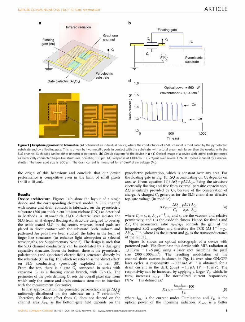
ResultsDevice architecture. Figures 1a,b show the layout of a singledevice and the corresponding electrical model. A SLG channelwith source and drain contacts is fabricated on the pyroelectricsubstrate (500 mm-thick z-cut lithium niobate (LN)) as describedin Methods. A 10 nm-thick Al2O3 dielectric layer isolates theSLG from an H-shaped floating Au structure designed to overlapthe oxide-coated SLG in the centre, whereas lateral pads areplaced in direct contact with the substrate. Both uniform andpatterned Au pads have been studied, the latter in the form offinger-like structures (to enhance light absorption at selectedwavelengths, see Supplementary Note 2). The design is such thatthe SLG channel conductivity can be modulated by a dual-gatecapacitive structure. From the bottom, there is the pyroelectricpolarization (and associated electric field) generated directly bythe substrate (C1 in Fig. 1b), which we refer to as the ‘direct effect’on SLG conductivity (previously exploited in ref. 38).From the top, there is a gate C2 connected in series withcapacitor C3 as a floating circuit branch, with C34C2. Theperimeter of the pads defining C3 sets the overall pixel size, fromwhich only the source and drain contacts stem out to interfacewith the measurement electronics.
In first approximation, the generated pyroelectric charge DQ isuniformly distributed on the substrate on a T variation1,2.Therefore, the direct effect from C1 does not depend on thechannel area AC1, as the bottom-gate field depends on the
pyroelectric polarization, which is constant over any area. Forthe floating gate in Fig. 1b, DQ accumulating on C3 depends onarea as (from equation (1)) DQ¼ pDTAC3. Being the structureelectrically floating and free from external parasitic capacitances,DQ is entirely provided by C2, because of the conservation ofcharge. A charged C2 generates for the SLG channel an effectivetop-gate voltage (in module):
DVTG¼DQC2
¼ pDTte0er
AC3
AC2ð4Þ
where C2¼ e0 er AC2 t� 1, e0 and er are the vacuum and relativepermittivity, and t is the oxide thickness. Hence, for fixed t andDT, the geometrical ratio AC3/AC2 controls the gain of theintegrated SLG amplifier and therefore the TCR (DI I� 1¼ gmDVTG I� 1, where I is the current and gm is the transconductanceof the GFET).
Figure 1c shows an optical micrograph of a device withpatterned pads. We illuminate this device with MIR radiation at1,100 cm� 1 (B9mm) using a laser spot matching the pixelsize (300� 300mm2). The resulting modulation of thechannel drain current is shown in Fig. 1d over nine ON/OFFlaser cycles. A responsivity B0.27mAW� 1 is obtained, for adrain current in the dark (IOFF) B1.3 mA (Vd¼ 10mV). Theresponsivity can be increased by applying a larger Vd, which, inturn, increases IOFF. The normalized current responsivity(%W� 1) is defined as:2
Rph;N¼ION � IOFF
IOFF� 100
Pinð5Þ
where ION is the current under illumination and Pin is theoptical power of the incoming radiation. Rpn,N is a better
Infrared radiation
Floatinggate (Au)
Graphenechannel
Vd
Vd
C1P(T)
C2C3
Floating gate
Pyroelectricsubstrate
Pyroelectricsubstrate
1.6Optical power = 560 µW
Wavenumber = 1,100 cm–1
1.5
1.4
1.3Dra
in c
urre
nt (
µA)
1.20 500 1,000
Time (s)
On
Off
Gate dielectric (Al2O3)
a b
c
d
Figure 1 | Graphene pyroelectric bolometer. (a) Scheme of an individual device, where the conductance of a SLG channel is modulated by the pyroelectric
substrate and by a floating gate. This is driven by two metallic pads in contact with the substrate, with a total area much larger than the overlap with the
SLG channel. Such pads can be either uniform or patterned. (b) Circuit diagram for the device in a. (c) Optical image of a device with lateral pads patterned
as electrically connected finger-like structures. Scalebar, 300 mm. (d) Response at 1,100 cm� 1 (B9mm) over several ON/OFF cycles induced by a manual
shutter. The laser spot size is 300mm. The drain current is measured for a 10mV drain voltage (Vd).
NATURE COMMUNICATIONS | DOI: 10.1038/ncomms14311 ARTICLE
NATURE COMMUNICATIONS | 8:14311 | DOI: 10.1038/ncomms14311 | www.nature.com/naturecommunications 3
parameter to compare photoconductive detectors. Rpn,N in Fig. 1dis B2� 104 %W� 1, over two orders of magnitude higher thanref. 38, where only the direct effect was exploited (B1.2� 102
%W� 1)38.
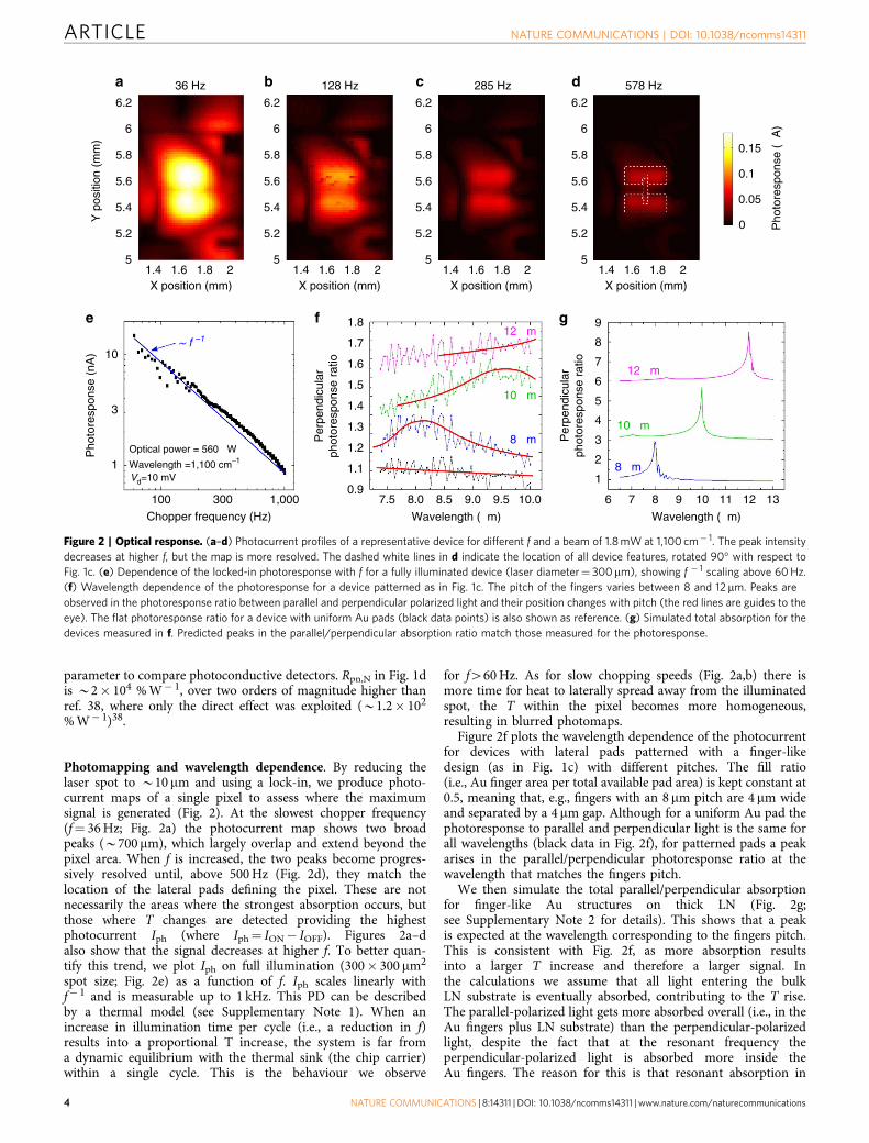
Photomapping and wavelength dependence. By reducing thelaser spot to B10 mm and using a lock-in, we produce photo-current maps of a single pixel to assess where the maximumsignal is generated (Fig. 2). At the slowest chopper frequency(f¼ 36Hz; Fig. 2a) the photocurrent map shows two broadpeaks (B700mm), which largely overlap and extend beyond thepixel area. When f is increased, the two peaks become progres-sively resolved until, above 500Hz (Fig. 2d), they match thelocation of the lateral pads defining the pixel. These are notnecessarily the areas where the strongest absorption occurs, butthose where T changes are detected providing the highestphotocurrent Iph (where Iph¼ ION� IOFF). Figures 2a–dalso show that the signal decreases at higher f. To better quan-tify this trend, we plot Iph on full illumination (300� 300 mm2
spot size; Fig. 2e) as a function of f. Iph scales linearly withf� 1 and is measurable up to 1 kHz. This PD can be describedby a thermal model (see Supplementary Note 1). When anincrease in illumination time per cycle (i.e., a reduction in f)results into a proportional T increase, the system is far froma dynamic equilibrium with the thermal sink (the chip carrier)within a single cycle. This is the behaviour we observe
for f460Hz. As for slow chopping speeds (Fig. 2a,b) there ismore time for heat to laterally spread away from the illuminatedspot, the T within the pixel becomes more homogeneous,resulting in blurred photomaps.
Figure 2f plots the wavelength dependence of the photocurrentfor devices with lateral pads patterned with a finger-likedesign (as in Fig. 1c) with different pitches. The fill ratio(i.e., Au finger area per total available pad area) is kept constant at0.5, meaning that, e.g., fingers with an 8 mm pitch are 4 mm wideand separated by a 4 mm gap. Although for a uniform Au pad thephotoresponse to parallel and perpendicular light is the same forall wavelengths (black data in Fig. 2f), for patterned pads a peakarises in the parallel/perpendicular photoresponse ratio at thewavelength that matches the fingers pitch.
We then simulate the total parallel/perpendicular absorptionfor finger-like Au structures on thick LN (Fig. 2g;see Supplementary Note 2 for details). This shows that a peakis expected at the wavelength corresponding to the fingers pitch.This is consistent with Fig. 2f, as more absorption resultsinto a larger T increase and therefore a larger signal. Inthe calculations we assume that all light entering the bulkLN substrate is eventually absorbed, contributing to the T rise.The parallel-polarized light gets more absorbed overall (i.e., in theAu fingers plus LN substrate) than the perpendicular-polarizedlight, despite the fact that at the resonant frequency theperpendicular-polarized light is absorbed more inside theAu fingers. The reason for this is that resonant absorption in
6.2
36 Hz 128 Hz 285 Hz 578 Hz
0.15
0.1
0.05
0 Pho
tore
spon
se (
µA)6
5.8
Y p
ositi
on (
mm
)
5.6
5.4
5.2
5
6.2
6
5.8
5.6
5.4
5.2
5
6.2
6
5.8
5.6
5.4
5.2
5
6.2
6
5.8
5.6
5.4
5.2
5
X position (mm)1.4
10
1.8 9
8
7
6
5
4
3
2
1
1.7
1.6
1.5
1.4
1.3
Per
pend
icul
arph
otor
espo
nse
ratio
Per
pend
icul
arph
otor
espo
nse
ratio
1.2
1.1
0.9
Pho
tore
spon
se (
nA)
3
Optical power = 560 µW
Wavelength =1,100 cm–1
Vd=10 mV1
100 300 1,000 7.5 8.0 8.5 9.0 9.5 10.0 6 7 8 9 10 11 12 13
8 µm
8 µm
10 µm
10 µm
12 µm
12 µm
Chopper frequency (Hz) Wavelength (µm) Wavelength (µm)
1.6 1.8 2X position (mm)
1.4 1.6 1.8 2X position (mm)
1.4 1.6 1.8 2X position (mm)
1.4 1.6 1.8 2
a b c d
e f g
~ f –1
Figure 2 | Optical response. (a–d) Photocurrent profiles of a representative device for different f and a beam of 1.8mW at 1,100 cm� 1. The peak intensity
decreases at higher f, but the map is more resolved. The dashed white lines in d indicate the location of all device features, rotated 90� with respect to
Fig. 1c. (e) Dependence of the locked-in photoresponse with f for a fully illuminated device (laser diameter¼ 300mm), showing f � 1 scaling above 60Hz.
(f) Wavelength dependence of the photoresponse for a device patterned as in Fig. 1c. The pitch of the fingers varies between 8 and 12 mm. Peaks are
observed in the photoresponse ratio between parallel and perpendicular polarized light and their position changes with pitch (the red lines are guides to the
eye). The flat photoresponse ratio for a device with uniform Au pads (black data points) is also shown as reference. (g) Simulated total absorption for the
devices measured in f. Predicted peaks in the parallel/perpendicular absorption ratio match those measured for the photoresponse.
ARTICLE NATURE COMMUNICATIONS | DOI: 10.1038/ncomms14311
4 NATURE COMMUNICATIONS | 8:14311 | DOI: 10.1038/ncomms14311 | www.nature.com/naturecommunications
the fingers is also accompanied by resonant reflection, whichlowers the overall delivery of light into the Au-LN systemas 1� resonant reflection. Things would change if thesedevices were fabricated on pyroelectric layers having a thicknessB1mm (rather than a 500 mm-thick LN crystal). The absorptionof the resonant structures would become dominant overthe intrinsic absorption of the substrate and reflectance wouldplay a minor role. Figure 2f proves that our device layout iswell suited for the implementation of photonic structures toengineer photon absorption and that a spectrally selectiveMIR response is feasible.
The data in Fig. 2 and the thermal model presented inSupplementary Note 1 suggest that better results could beobtained for devices with an optimized thermal managementcompared with that offered by a 500 mm-thick pyroelectricsubstrate. Indeed, the PDs in Figs 1 and 2 spend most of thephotons to heat the bulk rather than the surface, limiting theoverall T increase for a fixed incident power. The fabrication ofisolated pixels with lower heat capacity, using thin suspendedbridges or membranes (with typical thickness B1mm, asroutinely done for microbolometers)2, would improve theresponsivity, speed and wavelength selectivity.
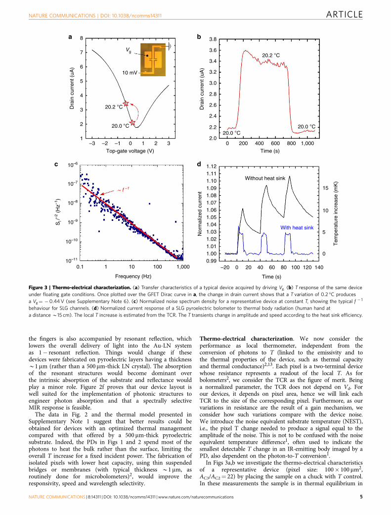
Thermo-electrical characterization. We now consider theperformance as local thermometer, independent from theconversion of photons to T (linked to the emissivity and tothe thermal properties of the device, such as thermal capacityand thermal conductance)2,13. Each pixel is a two-terminal devicewhose resistance represents a readout of the local T. As forbolometers2, we consider the TCR as the figure of merit. Beinga normalized parameter, the TCR does not depend on Vd. Forour devices, it depends on pixel area, hence we will link eachTCR to the size of the corresponding pixel. Furthermore, as ourvariations in resistance are the result of a gain mechanism, weconsider how such variations compare with the device noise.We introduce the noise equivalent substrate temperature (NEST),i.e., the pixel T change needed to produce a signal equal to theamplitude of the noise. This is not to be confused with the noiseequivalent temperature difference1, often used to indicate thesmallest detectable T change in an IR-emitting body imaged by aPD, also dependent on the photon-to-T conversion1.
In Figs 3a,b we investigate the thermo-electrical characteristicsof a representative device (pixel size: 100� 100 mm2,AC3/AC2¼ 22) by placing the sample on a chuck with T control.In these measurements the sample is in thermal equilibrium in
3.8
3.6
3.4
3.2
3.0
2.8
2.6
2.4
2.2
2.0
1.121.11
15
10
5
Tem
pera
ture
incr
ease
(m
K)
0
1.101.091.081.071.06
Nor
mal
ized
cur
rent
1.051.041.031.021.011.000.99
–20 0 20 40 60 80 100 120 140
Dra
in c
urre
nt (
uA)
Dra
in c
urre
nt (
uA)
20.0 °C
20.2 °C
10 mV
Vg
10–6
10–7
10–8
10–9
10–10
10–11
0.1 1 10
Frequency (Hz)
100 1,000
–3 –2 –1 0 1 2 3 0 200 400 600 800 1,000
Time (s)
Without heat sink
With heat sink
Top-gate voltage (V)
Sl /
–2 (
Hz–1
)
20.0 °C20.0 °C
20.2 °C
Time (s)
4
8
7
6
5
3
2
1
~ f –1
a b
c d
Figure 3 | Thermo-electrical characterization. (a) Transfer characteristics of a typical device acquired by driving Vg. (b) T response of the same device
under floating gate conditions. Once plotted over the GFET Dirac curve in a, the change in drain current shows that a T variation of 0.2 �C produces
a Vg¼ �0.44V (see Supplementary Note 6). (c) Normalized noise spectrum density for a representative device at constant T, showing the typical f � 1
behaviour for SLG channels. (d) Normalized current response of a SLG pyroelectric bolometer to thermal body radiation (human hand at
a distance B15 cm). The local T increase is estimated from the TCR. The T transients change in amplitude and speed according to the heat sink efficiency.
NATURE COMMUNICATIONS | DOI: 10.1038/ncomms14311 ARTICLE
NATURE COMMUNICATIONS | 8:14311 | DOI: 10.1038/ncomms14311 | www.nature.com/naturecommunications 5
the dark and photon absorption plays no role, thus uniformAu pads are chosen to accommodate (when needed) an electricalprobe on the gate pads and apply an external gate voltage (Vg) tothe device. Figure 3a shows a typical Dirac curve for a GFET atT¼ 20 �C. When an active electrical probe is connected to thegate pad, it acts as a sink neutralizing all the charge generated bythe pyroelectric material (C3) on any T change. Because of this,we measure the same transfer characteristics at all T, except forthe small shift induced by the direct bottom gating (C1) of thesubstrate (B5%K� 1; see Supplementary Note 3). The vastmajority of our devices are slightly p-doped (hole densityB2.5–3� 1012 cm� 2, in agreement with our Raman data, seeMethods), which is the ideal condition to achieve a maximumsignal on heating. This is linked to our choice of placing SLG onthe positive face of z-cut LN, where heating reduces the net dipolemoment, equivalent to a negative Vg
12. We stress that the slightlyp-type behaviour is the reproducible result of our transfermethod, with a B80% yield in terms of consistent doping.Because of the passivation offered by the Al2O3 gate dielectric, theinitial SLG doping does not show significant variations overseveral months (see Supplementary Fig. 8). After removing thegate probe to leave the gate structure floating, we monitor theGFET drain current, while T is raised by 0.2 �C, kept constantfor 10min and then decreased to its original value. The resultingplot in Fig. 3b shows that the drain current increases by B50%for a 0.2 �C T change (TCRB250%K� 1), is stable over time andthen returns to its original value with negligible hysteresis. Thered star markers on the electrically driven Dirac curve in Fig. 3ashow how the SLG conductivity evolves when the gate isthermally driven as in Fig. 3b. This stable dc response overseveral minutes indicates that no appreciable leakage occursthrough the pyroelectric crystal and/or the GFET gate withina practical measurement timeframe. The initial bump to 3.6 mA inFig. 3b is due to the small overshoot of the chuck T at the endof the ramp.
To evaluate the NEST we measure the normalized noise powerspectrum for a representative device (Fig. 3c). The spectrum isdominated by f� 1 noise up to 1 kHz and closely resembles thosepreviously measured for SLG devices43. The channel area (L�W)normalized noise (SI I� 2)(L�W) is B5� 10� 7 mm2Hz� 1 at10Hz (considering our 20� 30mm2 SLG channel), which slightlyexceeds the typical range (B10� 8–10� 7 mm2Hz� 1) reportedfor SLG devices on SiO2 (ref. 43). Considering a pixel size of100� 100 mm2 and a TCR of B214%K� 1, we get for the devicein Fig. 3b a NEST B40 mKHz� 1/2 at 1Hz (NEST¼ (SI I� 2)1/2
TCR� 1). For the biggest pixel size (300� 300 mm2,TCR B600%K� 1), the minimum NEST is B15 mKHz� 1/2.For the MIR PD in Fig. 1, this T resolution translates into a noiseequivalent power (NEP) B5� 10� 7WHz� 1/2 at 1Hz(NEP¼ (SI I� 2)1/2 RphN� 1), almost one order of magnitude betterthan that in ref. 44. The associated detectivity at 1Hz isB6� 104 Jones (D*¼A1/2 NEP� 1, where A is the area of thepixel), which is promising, considering the limitations in termsof thermal conductivity and mass2.
To appreciate what these numbers mean in practice, we showin Fig. 3d the photoresponse of a large device (300� 300 mm2,TCR B600%K� 1) illuminated by the IR radiation emitted by ahuman hand at a distance of B15 cm. In one test thesample is placed directly on a large (200mm diameter) metalchuck (with heat sink, blue data) and in another it is placedin a concave plastic box that keeps it suspended, thus morethermally isolated (without heat sink, black data). Without heatsink, the PD heats up more (hence larger device responsivity),but its response and recovery are much slower. Even with heatsink, the proximity of the hand is easily detected. The saturationsignal is B3%, corresponding to a T increase B5mK. To the best
of our knowledge, the only RT SLG detector working at 10mmand able to allow human hand detection is described in ref. 29.This was fabricated on a suspended and very thin (o1 mm)SiN membrane, measured in vacuum and with a lock-in with10 s integration time29. Here we achieve the same result on a bulk(500 mm-thick) substrate with a resistive measurement in airwith 200ms integration time, indicating that our SLG-basedpyroelectric bolometer can provide far better performance(in terms of responsivity and speed) in equivalent conditions.
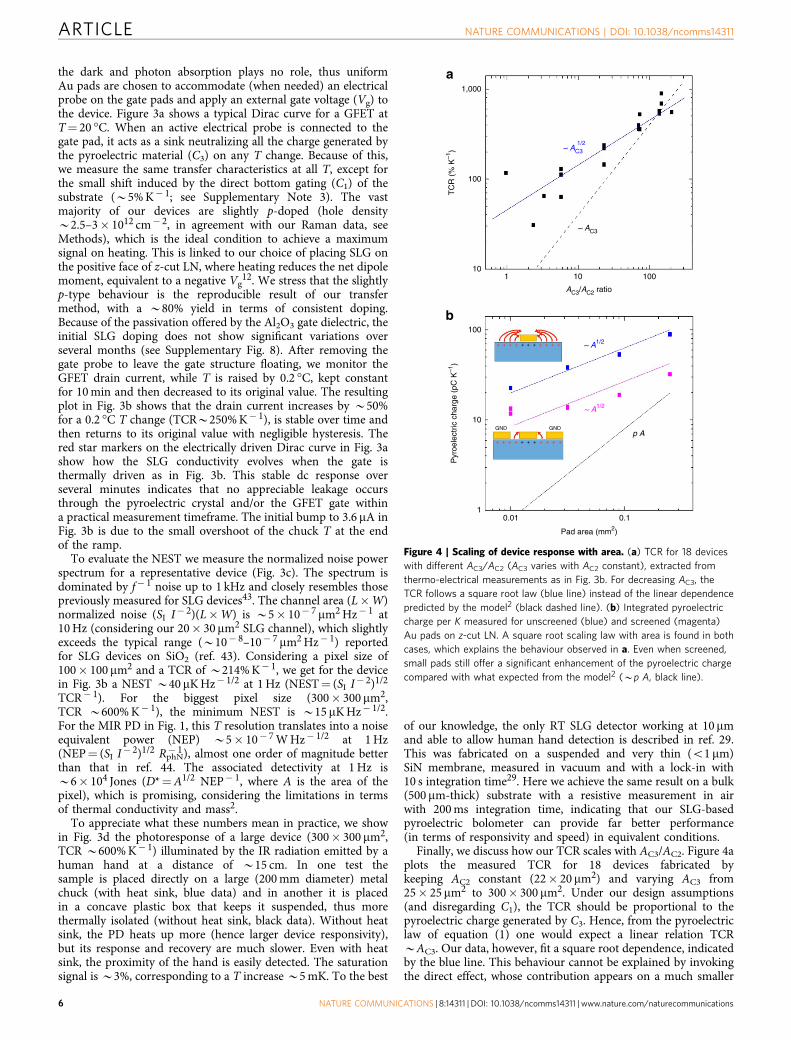
Finally, we discuss how our TCR scales with AC3/AC2. Figure 4aplots the measured TCR for 18 devices fabricated bykeeping AC2 constant (22� 20mm2) and varying AC3 from25� 25mm2 to 300� 300 mm2. Under our design assumptions(and disregarding C1), the TCR should be proportional to thepyroelectric charge generated by C3. Hence, from the pyroelectriclaw of equation (1) one would expect a linear relation TCRBAC3. Our data, however, fit a square root dependence, indicatedby the blue line. This behaviour cannot be explained by invokingthe direct effect, whose contribution appears on a much smaller
1,000
100
100
+ + + + + + + + + + +
+ + + + + + + + + + +
10GND GND
10.01 0.1
Pad area (mm2)
TC
R (
% K
–1)
Pyr
oele
ctric
cha
rge
(pC
K–1
)
101 10
AC3/AC2 ratio
p A
~ AC3
~ A1/2
~ A1/2
~ AC3
100
1/2
a
b
Figure 4 | Scaling of device response with area. (a) TCR for 18 devices
with different AC3/AC2 (AC3 varies with AC2 constant), extracted from
thermo-electrical measurements as in Fig. 3b. For decreasing AC3, the
TCR follows a square root law (blue line) instead of the linear dependence
predicted by the model2 (black dashed line). (b) Integrated pyroelectric
charge per K measured for unscreened (blue) and screened (magenta)
Au pads on z-cut LN. A square root scaling law with area is found in both
cases, which explains the behaviour observed in a. Even when screened,
small pads still offer a significant enhancement of the pyroelectric charge
compared with what expected from the model2 (Bp A, black line).
ARTICLE NATURE COMMUNICATIONS | DOI: 10.1038/ncomms14311
6 NATURE COMMUNICATIONS | 8:14311 | DOI: 10.1038/ncomms14311 | www.nature.com/naturecommunications
scale (TCR B5%K� 1, see Supplementary Note 3). Rather, wehave to consider that the pyroelectric substrate does not endat the pads edge. Such pads are thus not driven just by thecrystal below them (as assumed by a linear dependence on area),but can also be affected by the exposed polarization of theirsurrounding areas (an effect scaling linearly with perimeter, hencethe square root dependence on area). To better quantify thisbehaviour, we prepare Au pads of different sizes (0.01–0.3mm2)on our pyroelectric substrates and measure the total chargegenerated on heating (Fig. 4b). This is accomplished by placing anelectric probe on each pad, connecting the probe to groundand integrating the pyroelectric current flowing through theprobe over the whole temperature ramp. In one case, the pads arekept isolated on the 1� 1 cm2 pyroelectric surface and indepen-dent from each other. In another case, the whole surface aroundthe pads is coated with Au and grounded during all measure-ments (with only a gap of 5 mm uncoated around the pads).This is meant to suppress any contribution from areas beyond thepad footprint. Figure 4b shows that a square root dependenceon pad area is observed in both cases. The total pyroelectriccharge decreases by a factor B2–3 on screening, but is still abovewhat would be expected from the model2 Q DT� 1¼ p A evenfor relatively large pads (using P¼ 77 mCm� 2 K, as measured fora LN sample fully covered with Au and consistently withliterature2,12,45). This result has major technological implications,as it proves that a substantial contribution to the observedTCR enhancement for small AC3 arises within the firstfew micrometres from the pad edge. It is then possible toharvest an enhanced pyroelectric charge in a dense array ofsmall pixels, with only a tiny gap of few micrometres separatingtwo adjacent devices.
DiscussionIn principle, AC3/AC2 410 is desirable, because it can deliverTCRs up to 900%K� 1 (Fig. 4a and Supplementary Fig. 7), butthis upscaling is bound by the maximum gate voltage variationallowed for the GFET (dynamic range). When probed electrically(Fig. 3a), our GFETs show no gate leakage up to ±5V
(B5MV cm� 1). Beyond this value, dielectric breakdown canoccur. This determines the maximum thermal shocka device can sustain without failing, inversely proportionalto the TCR. However, this is not a concern if the environmentT is drifting on a timescale much larger than the measurementtimeframe, e.g., during a day/night indoor T cycle. Althoughinternal pyroelectric leakage can be neglected overa few minutes, it can still discharge a device completely overlonger timeframes. This will always leave the GFET at the bestoperating point to respond to sudden signals (see SupplementaryNote 4). If one wants to scale down the pixel size whilemaintaining the same area ratio, the channel area must bedecreased accordingly. As the 1/f noise scales with channel area43,we can expect the GFET noise to increase and cancel thebenefit of a large TCR when the NEST is evaluated. However,Fig. 4 shows that the TCR scales sub-linearly with area. Forpixels approaching the scale required for high-resolutionIR cameras (20� 20mm2)2, it is better to make a large (severalmicrometres) channel and accept a lower area ratio(e.g., AC3/AC2 o10), because the small price paid in terms ofTCR will be more than compensated by lower noise,a less critical lithographic process and a detector more resilientto sudden thermal shocks.
In conclusion, we presented a graphene-based pyroelectricbolometer operating at room temperature with TCR up toB900%K� 1 for a device area B300� 300 mm2 able to resolvetemperature variations down to 15mK at 1Hz. For smallerdevices, the TCR scales sub-linearly with area, due to anenhancement of the collected pyroelectric charge in closeproximity to the metallic edges. When used as MIR PDs, ourdevices deliver very promising performance (in terms ofresponsivity, speed and NEP) even on bulk substrates and arecapable to detect warm bodies in their proximity. Spectralselectivity can be achieved by patterning resonant structures aspart of the pixel layout. This technology is competitive ona number of levels, ranging from high-resolution thermalimaging (small pixel limit) to highly sensitive spectroscopy inthe MIR and far-IR (large pixel limit).
Device DeviceIn
tens
ity (
a.u.
)
Inte
nsity
(a.
u.)
Transfer
Transfer
SLG on Cu
1,250 1,500 1,750 2,600 2,800
Raman shift (cm–1)
1,250 1,500 2,600 2,800
Raman shift (cm–1)
G G
2D 2D
(D)
LN substrate
a b
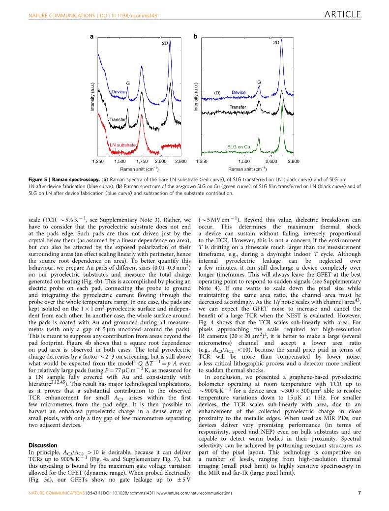
Figure 5 | Raman spectroscopy. (a) Raman spectra of the bare LN substrate (red curve), of SLG transferred on LN (black curve) and of SLG on
LN after device fabrication (blue curve). (b) Raman spectrum of the as-grown SLG on Cu (green curve), of SLG film transferred on LN (black curve) and of
SLG on LN after device fabrication (blue curve) and subtraction of the substrate contribution.
NATURE COMMUNICATIONS | DOI: 10.1038/ncomms14311 ARTICLE
NATURE COMMUNICATIONS | 8:14311 | DOI: 10.1038/ncomms14311 | www.nature.com/naturecommunications 7
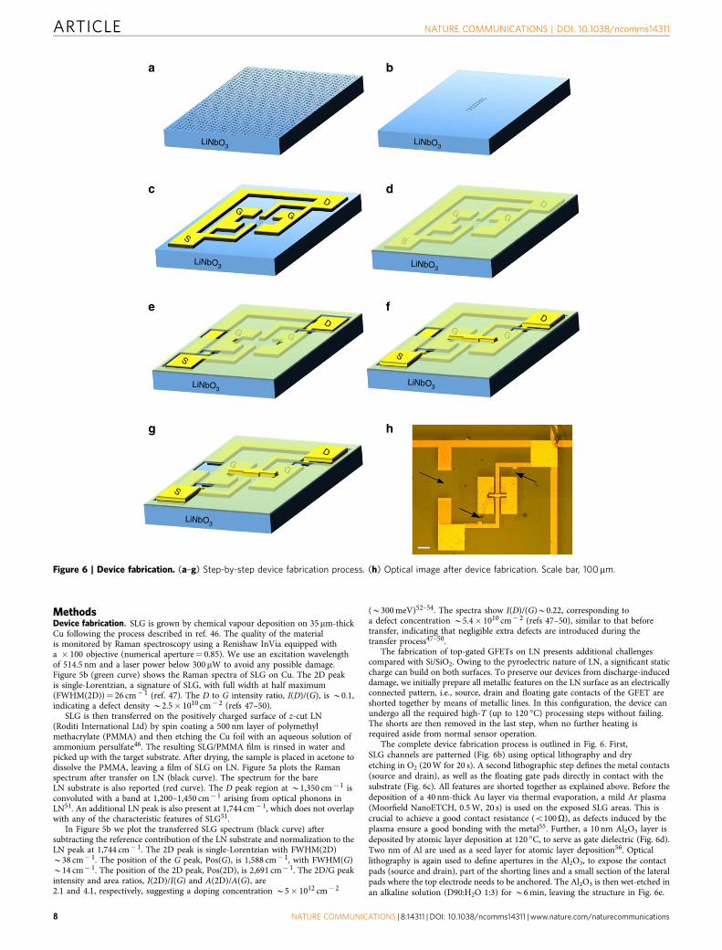
MethodsDevice fabrication. SLG is grown by chemical vapour deposition on 35 mm-thickCu following the process described in ref. 46. The quality of the materialis monitored by Raman spectroscopy using a Renishaw InVia equipped witha � 100 objective (numerical aperture¼ 0.85). We use an excitation wavelengthof 514.5 nm and a laser power below 300 mW to avoid any possible damage.Figure 5b (green curve) shows the Raman spectra of SLG on Cu. The 2D peakis single-Lorentzian, a signature of SLG, with full width at half maximum(FWHM(2D))¼ 26 cm� 1 (ref. 47). The D to G intensity ratio, I(D)/(G), is B0.1,indicating a defect density B2.5� 1010 cm� 2 (refs 47–50).
SLG is then transferred on the positively charged surface of z-cut LN(Roditi International Ltd) by spin coating a 500 nm layer of polymethylmethacrylate (PMMA) and then etching the Cu foil with an aqueous solution ofammonium persulfate46. The resulting SLG/PMMA film is rinsed in water andpicked up with the target substrate. After drying, the sample is placed in acetone todissolve the PMMA, leaving a film of SLG on LN. Figure 5a plots the Ramanspectrum after transfer on LN (black curve). The spectrum for the bareLN substrate is also reported (red curve). The D peak region at B1,350 cm� 1 isconvoluted with a band at 1,200–1,450 cm� 1 arising from optical phonons inLN51. An additional LN peak is also present at 1,744 cm� 1, which does not overlapwith any of the characteristic features of SLG51.
In Figure 5b we plot the transferred SLG spectrum (black curve) aftersubtracting the reference contribution of the LN substrate and normalization to theLN peak at 1,744 cm� 1. The 2D peak is single-Lorentzian with FWHM(2D)B38 cm� 1. The position of the G peak, Pos(G), is 1,588 cm� 1, with FWHM(G)B14 cm� 1. The position of the 2D peak, Pos(2D), is 2,691 cm� 1. The 2D/G peakintensity and area ratios, I(2D)/I(G) and A(2D)/A(G), are2.1 and 4.1, respectively, suggesting a doping concentration B5� 1012 cm� 2
(B300meV)52–54. The spectra show I(D)/(G)B0.22, corresponding toa defect concentration B5.4� 1010 cm� 2 (refs 47–50), similar to that beforetransfer, indicating that negligible extra defects are introduced during thetransfer process47–50.
The fabrication of top-gated GFETs on LN presents additional challengescompared with Si/SiO2. Owing to the pyroelectric nature of LN, a significant staticcharge can build on both surfaces. To preserve our devices from discharge-induceddamage, we initially prepare all metallic features on the LN surface as an electricallyconnected pattern, i.e., source, drain and floating gate contacts of the GFET areshorted together by means of metallic lines. In this configuration, the device canundergo all the required high-T (up to 120 �C) processing steps without failing.The shorts are then removed in the last step, when no further heating isrequired aside from normal sensor operation.
The complete device fabrication process is outlined in Fig. 6. First,SLG channels are patterned (Fig. 6b) using optical lithography and dryetching in O2 (20W for 20 s). A second lithographic step defines the metal contacts(source and drain), as well as the floating gate pads directly in contact with thesubstrate (Fig. 6c). All features are shorted together as explained above. Before thedeposition of a 40 nm-thick Au layer via thermal evaporation, a mild Ar plasma(Moorfield NanoETCH, 0.5W, 20 s) is used on the exposed SLG areas. This iscrucial to achieve a good contact resistance (o100O), as defects induced by theplasma ensure a good bonding with the metal55. Further, a 10 nm Al2O3 layer isdeposited by atomic layer deposition at 120 �C, to serve as gate dielectric (Fig. 6d).Two nm of Al are used as a seed layer for atomic layer deposition56. Opticallithography is again used to define apertures in the Al2O3, to expose the contactpads (source and drain), part of the shorting lines and a small section of the lateralpads where the top electrode needs to be anchored. The Al2O3 is then wet-etched inan alkaline solution (D90:H2O 1:3) for B6min, leaving the structure in Fig. 6e.
LiNbO3LiNbO3
LiNbO3LiNbO3
G G
D
S
G G
D
S
G G
D
S
GG
D
S
G G
D
S
LiNbO3LiNbO3
LiNbO3
a b
c d
e f
g h
Figure 6 | Device fabrication. (a–g) Step-by-step device fabrication process. (h) Optical image after device fabrication. Scale bar, 100 mm.
ARTICLE NATURE COMMUNICATIONS | DOI: 10.1038/ncomms14311
8 NATURE COMMUNICATIONS | 8:14311 | DOI: 10.1038/ncomms14311 | www.nature.com/naturecommunications
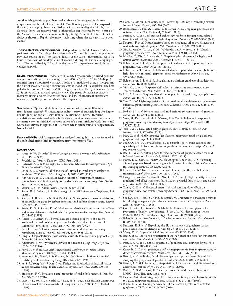
Another lithographic step is then used to finalize the top-gate via thermalevaporation and lift-off of 2/60 nm of Cr/Au. Bonding pads are also prepared inthis step, overlapping those deposited with the contacts (Fig. 6f). Finally, theelectrical shorts are removed with a lithographic step followed by wet-etching ofthe Au lines in an aqueous solution of KI:I2 (Fig. 6g). An optical picture of the finaldevice is shown in Fig. 6h, the arrows indicating where the Au shorts have beenetched.
Thermo-electrical characterization. T-dependent electrical characterization isperformed with a Cascade probe station with a T-controlled chuck, coupled to anHP4142B source meter. The spectral density of the current fluctuations (SI) is theFourier transform of the drain current recorded during 100 s with a sampling of1ms. The normalized SI I� 2 exhibits the same f � 1 dependence for all drainvoltages applied.
Device characterization. Devices are illuminated by a linearly polarized quantumcascade laser with a frequency range from 1,000 to 1,610 cm� 1 (B6.2–10 mm)scanned using a motorized xyz stage. The laser is modulated using a chopper andthe current measured using a current pre-amplifier and lock-in amplifier. The lightpolarization is controlled with a ZnSe wire grid polarizer. The light is focused usingZnSe lenses with numerical aperture B0.5. The power for each frequency ismeasured using a bolometric power meter and the photocurrent spectra arenormalized by this power to calculate the responsivity.
Simulations. Optical calculations are performed with a finite-differencetime-domain method57,58 assuming an infinite array of infinitely long Au fingers(40 nm-thick) on top of a semi-infinite LN substrate. Thermal transientcalculations are performed with a finite element method (see www.comsol.com)assuming a 500 mm-thick LN substrate on top of a 3mm-thick Au block (heat-sink)whose back surface is kept fixed at RT. More details can be found in SupplementaryNotes 1 and 2.
Data availability. All data generated or analysed during this study are included inthis published article (and its Supplementary Information files).
References1. Kruse, P. W. Uncooled Thermal Imaging Arrays, Systems and Applications
(SPIE Press, 2001).2. Rogalski, A. Infrared Detectors (CRC Press, 2011).3. Richards, P. L. & McCreight, C. R. Infrared detectors for astrophysics. Phys.
Today 58, 41–47 (2005).4. Jones, B. F. A reappraisal of the use of infrared thermal image analysis in
medicine. IEEE Trans. Med. Imaging 17, 1019–1027 (1998).5. Ahyeon, K. et al. Ultrathin injectable sensors of temperature, thermal
conductivity, and heat capacity for cardiac ablation monitoring. Adv. Health.Mater. 5, 373–381 (2016).
6. Meijer, G. C. M. Smart sensor systems (Wiley, 2008).7. Rudol, P. & Doherty, P. in Proceedings of the IEEE Aerospace Conference, 1–8
(2008).8. Kreuzer, L. B., Kenyon, N. D. & Patel, C. K. N. Air pollution: sensitive detection
of ten pollutant gases by carbon monoxide and carbon dioxide lasers. Science177, 347–349 (1972).
9. Evans, D. D. & Stroup, D. W. Methods to calculate the response time of heatand smoke detectors installed below large unobstructed ceilings. Fire Technol.22, 54–65 (1985).
10. Simon, I. & Arndt, M. Thermal and gas-sensing properties of a micro-machined thermal conductivity sensor for the detection of hydrogen inautomotive applications. Sens. Act. A 97, 104–108 (2002).
11. Yun, J. & Lee, S. Human movement detection and identification usingpyroelectric infrared sensors. Sensors 14, 8057–8081 (2014).
12. Lang, S. B. Pyroelectricity: from ancient curiosity to modern imaging tool. Phys.Today 58, 31–36 (2005).
13. Whatmore, R. W. Pyroelectric devices and materials. Rep. Prog. Phys. 49,1335–1386 (1986).
14. Purkl, F. et al. in IEEE 26th International Conference on Micro ElectroMechanical Systems (MEMS), 185–188 (2013).
15. Jerominek, H., Picard, F. & Vincent, D. Vanadium oxide films for opticalswitching and detection. Opt. Eng. 32, 2092–2099 (1993).
16. Ju, S.-B., Yong, Y.-J. & Kim, S.-G. Design and fabrication of high fill-factormicrobolometer using double sacrificial layers. Proc. SPIE 3698, 180–189(1999).
17. Brockman, F. G. Production and properties of nickel bolometers. J. Opt. Soc.Am. 36, 32–35 (1946).
18. Tissot, J. L., Rothan, F., Vedel, C., Vilain, M. & Yon, J.-J. LETI/LIR’s amorphoussilicon uncooled microbolometer development. Proc. SPIE 3379, 139–144(1998).
19. Hara, K., Omori, T. & Ueno, R. in Proceedings 12th IEEE Workshop NeuralNetwork Signal Process, 697–706 (2002).
20. Bonaccorso, F., Sun, Z., Hasan, T. & Ferrari, A. C. Graphene photonics andoptoelectronics. Nat. Photon. 4, 611–622 (2010).
21. Ferrari, A. C. et al. Science and technology roadmap for graphene, relatedtwo-dimensional crystals, and hybrid systems. Nanoscale 7, 4587–5062 (2015).
22. Koppens, F. et al. Photodetectors based on graphene, other two-dimensionalmaterials and hybrid systems. Nat. Nanotechnol. 9, 780–793 (2014).
23. Xia, F., Mueller, T., Lin, Y.-M., Valdes-Garcia, A. & Avouris, P. Ultrafastgraphene photodetector. Nat. Nanotechnol. 4, 839–843 (2009).
24. Mueller, T., Xia, F. & Avouris, P. Graphene photodetectors for high-speedoptical communications. Nat. Photonics 4, 297–301 (2010).
25. Echtermeyer, T. J. et al. Strong plasmonic enhancement of photovoltage ingraphene. Nat. Commun. 2, 458 (2011).
26. Echtermeyer, T. J. et al. Photothermoelectric and photoelectric contributions tolight detection in metal–graphene–metal photodetectors. Nano Lett. 14,3733–3742 (2014).
27. Echtermeyer, T. J. et al. Surface plasmon polariton graphene photodetectors.Nano Lett. 16, 8–20 (2015).
28. Vicarelli, L. et al. Graphene field effect transistors as room-temperatureTerahertz detectors. Nat. Mater. 11, 865–871 (2012).
29. Hsu, A. L et al. Graphene-based thermopile for thermal imaging applications.Nano Lett. 15, 7211–7216 (2015).
30. Yao, Y. et al. High-responsivity mid-infrared graphene detectors with antenna-enhanced photocarrier generation and collection. Nano Lett. 14, 3749–3754(2014).
31. Badioli, M. et al. Phonon-mediated mid-infrared photoresponse of graphene.Nano Lett. 14, 6374–6381 (2014).
32. Vora, H., Kumaravadivel, P., Nielsen, B. & Du, X. Bolometric response ingraphene based superconducting tunnel junctions. Appl. Phys. Lett. 100,153507 (2012).
33. Yan, J. et al. Dual-gated bilayer graphene hot-electron bolometer. Nat.Nanotechnol. 7, 472–478 (2012).
34. Han, Q. et al. Highly sensitive hot electron bolometer based on disorderedgraphene. Sci. Rep. 3, 1–6 (2013).
35. Shao, Q., Liu, G., Teweldebrhan, D. & Balandin, A. A. High-temperaturequenching of electrical resistance in graphene interconnects. Appl. Phys. Lett.92, 202108 (2008).
36. Bae, J. J. et al. Sensitive photo-thermal response of graphene oxide for mid-infrared detection. Nanoscale 7, 15695–15700 (2015).
37. Hazra, K. S., Sion, N., Yadav, A., McLauhglin, J. & Misra, D. S. Verticallyaligned graphene based non-cryogenic bolometer. Preprint at https://arxiv.org/ftp/arxiv/papers/1301/1301.1302 (2013).
38. Hsieh, C. et al. Graphene-lead zirconate titanate optothermal field effecttransistors. Appl. Phys. Lett. 100, 113507 (2012).
39. Hong, X., Posadas, A., Zou, K., Ahn, C. H. & Zhu, J. High-mobility few-layergraphene field effect transistors fabricated on epitaxial ferroelectric gate oxides.Phys. Rev. Lett. 102, 136808 (2009).
40. Zhang, C. X. et al. Electrical stress and total ionizing dose effects ongraphene-based non-volatile memory devices. IEEE Trans. Nucl. Sci. 59, 2974(2012).
41. Qian, Z., Liu, F., Hui, Y., Kar, S. & Rinaldi, M. Graphene as a massless electrodefor ultrahigh-frequency piezoelectric nanoelectromechanical systems. NanoLett. 15, 4599–4604 (2015).
42. Guo, Y., Akai, D., Swada, K. & Ishida, M. Ferroelectric and pyroelectricproperties of highly (110)-oriented Pb(Zr0.4Ti0.6)O3 thin films grown onPt-LaNiO3-SiO2-Si substrates. App. Phys. Lett. 90, 232908 (2007).
43. Balandin, A. A. Low-frequency 1/f noise in graphene devices. Nat. Nanotech.8, 549–555 (2013).
44. Kulkarni, E. S. et al. Exploiting the IR transparency of graphene for fastpyroelectric infrared detection. Adv. Opt. Mat 3, 34–38 (2015).
45. Wong, K. K. Properties of Lithium Niobate (INSPEC, 2002).46. Bae, S. et al. Roll-to-roll production of 30-inch graphene films for transparent
electrodes. Nat. Nanotech. 5, 574–578 (2010).47. Ferrari, A. C. et al. Raman spectrum of graphene and graphene layers. Phys.
Rev. Lett. 97, 187401 (2006).48. Cancado, L. G. et al. quantifying defects in graphene via Raman spectroscopy at
different excitation energies. Nano Lett. 11, 3190–3196 (2011).49. Ferrari, A. C. & Basko, D. M. Raman spectroscopy as a versatile tool for
studying the properties of graphene. Nat. Nanotech. 8, 235–246 (2013).50. Ferrari, A. C. & Robertson, J. Interpretation of Raman spectra of disordered and
amorphous carbon. Phys. Rev. B 61, 14095 (2000).51. Barker, A. S. & Loudon, R. Dielectric properties and optical phonons in
LiNbO3. Phys. Rev. 158, 433 (1967).52. Das, A. et al. Monitoring dopants by Raman scattering in an electrochemically
top-gated graphene transistor. Nat. Nanotech. 3, 210–215 (2008).53. Bruna, M. et al. Doping dependence of the Raman spectrum of defected
graphene. ACS Nano 8, 7432–7441 (2014).
NATURE COMMUNICATIONS | DOI: 10.1038/ncomms14311 ARTICLE
NATURE COMMUNICATIONS | 8:14311 | DOI: 10.1038/ncomms14311 | www.nature.com/naturecommunications 9
54. Basko, D. M., Piscanec, S. & Ferrari, A. C. Electron-electron interactions anddoping dependence of the two-phonon Raman intensity in graphene. Phys. Rev.B 80, 165413 (2009).
55. Choi, M. S., Lee, S. H. & Yoo, W. Plasma treatments to improve metal contactsin graphene field effect transistor. J. Appl. Phys. 110, 073305 (2011).
56. Kim, S. et al. Realization of a high mobility dual-gated graphene field-effecttransistor with Al2O3 dielectric. Appl. Phys. Lett. 94, 062107 (2009).
57. Taflove, A. & Hagness, S. C. Computational Electrodynamics: The FDTDMethod (Artech House, 2005).
58. Lidorikis, E., Egusa, E. & Joannopoulos, J. D. Effective medium properties andphotonic crystal superstructures of metallic nanoparticle arrays. J. Appl. Phys.101, 054304 (2007).
AcknowledgementsWe acknowledge funding from EU Graphene Flagship, ERC Grant Hetero2D and EPSRCGrant Numbers EP/ 509 K01711X/1, EP/K017144/1, EP/N010345/1, EP/M507799/ 5101and EP/L016087/1. We thank Graphenea for provision of some chemical vapourdeposition graphene samples on LiNbO3.
Author contributionsA.C. conceived the idea. A.C., S.B. and A.C.F. led the research. A.C. and U.S. optimizedthe device layout, developed and performed the device fabrication process, and per-formed thermo-electrical characterization. U.S. and D.D.F. prepared andtransferred the graphene films. Z.Z. performed Al2O3 characterization. R.P., S.N.,U.S., and F.H.L.K. performed the optical characterization in the MIR and measuredthe noise spectra. E.L. performed the simulations for the wavelength dependenceand the thermal model. U.S., M.B. and A.C.F performed the Raman analysis.
All authors discussed the results, contributed to data analysis and assisted in manuscriptpreparation.
Additional informationSupplementary Information accompanies this paper at http://www.nature.com/naturecommunications
Competing financial interests: The authors declare no competing financial interests.
Reprints and permission information is available online at http://npg.nature.com/reprintsandpermissions/
How to cite this article: Sassi, U. et al. Graphene-based mid-infrared room-temperaturepyroelectric bolometers with ultrahigh temperature coefficient of resistance.Nat. Commun. 8, 14311 doi: 10.1038/ncomms14311 (2017).
Publisher’s note: Springer Nature remains neutral with regard to jurisdictional claims inpublished maps and institutional affiliations.
This work is licensed under a Creative Commons Attribution 4.0International License. The images or other third party material in this
article are included in the article’s Creative Commons license, unless indicated otherwisein the credit line; if the material is not included under the Creative Commons license,users will need to obtain permission from the license holder to reproduce the material.To view a copy of this license, visit http://creativecommons.org/licenses/by/4.0/
r The Author(s) 2017
ARTICLE NATURE COMMUNICATIONS | DOI: 10.1038/ncomms14311
10 NATURE COMMUNICATIONS | 8:14311 | DOI: 10.1038/ncomms14311 | www.nature.com/naturecommunications