Surface Oxygen Technology for Graphene Production
11
1 Surface Oxygen Technology for Graphene Production Prepared by: Vanissa B. Gale Stephen G. Abelada
Transcript of Surface Oxygen Technology for Graphene Production
1
Surface Oxygen Technology
for Graphene Production
Prepared by:
Vanissa B. Gale
Stephen G. Abelada
2
Graphene: An unusual wonder material
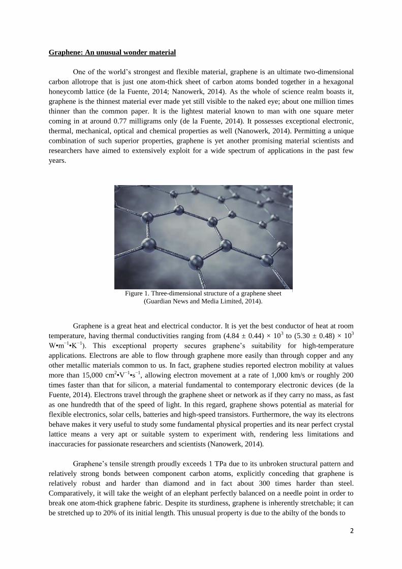
One of the world’s strongest and flexible material, graphene is an ultimate two-dimensional
carbon allotrope that is just one atom-thick sheet of carbon atoms bonded together in a hexagonal
honeycomb lattice (de la Fuente, 2014; Nanowerk, 2014). As the whole of science realm boasts it,
graphene is the thinnest material ever made yet still visible to the naked eye; about one million times
thinner than the common paper. It is the lightest material known to man with one square meter
coming in at around 0.77 milligrams only (de la Fuente, 2014). It possesses exceptional electronic,
thermal, mechanical, optical and chemical properties as well (Nanowerk, 2014). Permitting a unique
combination of such superior properties, graphene is yet another promising material scientists and
researchers have aimed to extensively exploit for a wide spectrum of applications in the past few
years.
Graphene is a great heat and electrical conductor. It is yet the best conductor of heat at room
temperature, having thermal conductivities ranging from (4.84 ± 0.44) × 103 to (5.30 ± 0.48) × 10
3
W•m−1
•K−1
). This exceptional property secures graphene’s suitability for high-temperature
applications. Electrons are able to flow through graphene more easily than through copper and any
other metallic materials common to us. In fact, graphene studies reported electron mobility at values
more than 15,000 cm2•V
−1•s
−1, allowing electron movement at a rate of 1,000 km/s or roughly 200
times faster than that for silicon, a material fundamental to contemporary electronic devices (de la
Fuente, 2014). Electrons travel through the graphene sheet or network as if they carry no mass, as fast
as one hundredth that of the speed of light. In this regard, graphene shows potential as material for
flexible electronics, solar cells, batteries and high-speed transistors. Furthermore, the way its electrons
behave makes it very useful to study some fundamental physical properties and its near perfect crystal
lattice means a very apt or suitable system to experiment with, rendering less limitations and
inaccuracies for passionate researchers and scientists (Nanowerk, 2014).
Graphene’s tensile strength proudly exceeds 1 TPa due to its unbroken structural pattern and
relatively strong bonds between component carbon atoms, explicitly conceding that graphene is
relatively robust and harder than diamond and in fact about 300 times harder than steel.
Comparatively, it will take the weight of an elephant perfectly balanced on a needle point in order to
break one atom-thick graphene fabric. Despite its sturdiness, graphene is inherently stretchable; it can
be stretched up to 20% of its initial length. This unusual property is due to the abilty of the bonds to
Figure 1. Three-dimensional structure of a graphene sheet
(Guardian News and Media Limited, 2014).

3
be twisted, pulled and curved to a certain extent without experiencing breakage (Brewster, 2013;
Nanowerk, 2014).
In chemical properties aspect, graphene, similar to graphite surface, can adsorb and desorb
various atoms and molecules including NO2, NH3, K and hydroxides. It can also be functionalized and
activated by several chemical groups, for instance, OH- and F- groups, creating graphene oxide and
fluorinated graphene, materials of varied applications especially in medicine and electronics
(AzoNano, 2014; Nanowerk, 2014).
An almost completely transparent material, graphene is able to optically transmit more than
90% of light and 2.3% of visible light that hits or strikes it. This is a major requirement for
optoelectronic applications. Since graphene is as well highly conductive, it would work very well in
optoelectronic devices particularly as an LCD touch screen material (Brewster, 2013; Nanowerk,
2014).
Applications and Relevance to Society
With the many excellent properties of graphene mentioned, its applications extend but are not
limited to numerous disciplines vital to current societal endeavors including bioengineering,
optolectronics and electronics, composite materials, energy technology and nanotechnology.
Figure 2. Conductive graphene-based material (Plastic
Electronics, 2012).
Figure 3. Graphene-based coating (Hsu, 2012).
Figure 4. Graphene-oxide paper (Graphene
Supermarket, nd).
Figure 5. Graphene in Nokia’s “HumanForm”
concept phone (xtremevbtalk, 2014).

4
Graphene poses a vital part in the future of bioengineering. With graphene offering a large
surface area, high electrical conductivity, thinness and strength, it would make an excellent candidate
for the development of fast and efficient bioelectric sensory devices. These devices, if manufactured
with graphene, then will possess the ability to monitor crucial and sensitive parameters such as
glucose, hemoglobin and cholesterol levels in the blood and even DNA sequencing at more
convenient and accurate levels than existing ones (Nanowerk, 2014).
In the field of optoelectronics, indium tin oxide (ITO) is the current material utilized as
coating particularly for transparent LCD screens. However, recent tests have shown that graphene is
certainly able to match the properties of ITO (Nanowerk, 2014). With its high tensile strength,
thinness, flexibility and optical properties, existing optoelectronic devices may be replaced by more
robust, stretchable and transparent ones. It is in fact a prospective candidate for competition counter to
bendable ITO electronics that will soon hit consumer markets. As to electronics, research has mostly
focused on making computer chips more powerful by packing in more transistors while
simultaneously making such transistors more potent by hastening the electron flow. Computer chips
rely on billions of transistors to control the flow of electricity in their circuits. As science approaches
the limit for how small transistors can be, graphene could push the limit back by both moving
electrons in transistors faster and reducing their very size to a few atoms or less (Brewster, 2013).
Figure 6. Optical image of a graphene wireless
sensor biotransferred onto the surface of a tooth
(Berger, 2014).
Figure 7. Transistors manufactured by Intel at
32 nanometer-sizes (Brewster, 2013).

5
With graphene being much stronger at the same time much lighter, the use of steel for
manufacture of aircraft structures and materials is gradually replaced by a composite material
employing graphene integrated to carbon fiber, significantly improving fuel efficiency, reducing
aircraft weight and hence increasing flight range. Due to its electrical conductivity as well, graphene
could even be used to coat aircraft surface material to prevent electrical damage resulting from
lightning strikes. In this application, the same graphene coating could be utilized to measure strain
rate, notifying the pilot of any changes in the stress levels that the aircraft wings are under. Moreover,
these characteristics can help in the development of high strength-requirement applications such as
body armor for military personnel and vehicles (Nanowerk, 2014).
In relation to energy technology, graphene is a prospective material for revolutionizing solar
cell mass production. Solar cells rely on semiconductors to absorb sunlight. Today’s semiconductors
are made of silicon having two electron layers. Solar cells work by transferring the energy from light
particles to the calm electrons in one layer, which eventually become excited and jump to the free-
flowing electrons layer, hence creating electricity. Graphene’s layers of electron networks overlap,
indicating that less light energy is needed to get the electrons to jump between layers. This property
perceptibly could raise solar cell energy efficiency. Using graphene would also allow manufacture of
solar cells that are hundreds of thousands of times thinner and lighter than those that rely on silicon
(Brewster, 2013).
Figure 8. Formula One car made of carbon
fiber with graphene (Autosavant, 2008).
Figure 9. Solar cell installation (Laden, 2013).

6
Major Barriers to Graphene Production
With the numerous excellent properties and the seem-to-be endless possibilities for its
applications, the question remains as to why graphene commercialization is not fully realized; why
graphene remains behind laboratory bars and is not perceptibly competing in the global industrial
markets? The answer lies on the current graphene size, structure, quality and method of production.
One of the greatest challenges faced today in commercializing graphene is how to produce
large, single, high-quality crystals in an environmentally-friendly reproducible manner at low cost.
Graphene has always been grown in a polycrystalline form, that is, it is composed of many small
crystals that are joined together with irregular chemical bonding at their boundaries (“grain
boundaries”), something like a patch-work quilt. Large, single-crystal graphene is of great interest
because the grain boundaries in polycrystalline material have defects and may house several impurity
substances. Eliminating such defects hence implies a better material of superior qualities (Science
Daily, 2013). It may sound simple to just create graphene that exemplify what key player industries
nowadays consider as ideal. However, it is very difficult to produce large, single-crystalline graphene
thin films possessing very high electrical and thermal conductivities along with excellent optical
transparency, at least not with the current methods available to us.
Another issue of grave concern is that synthesis of graphene by conventional methods
involves the use of toxic chemicals that usually result in the generation of hazardous waste and
poisonous gases. Furthermore, the complexity of several of these methods entails associated high
production cost for graphene which, consequently, yields a high-cost end material, that is, graphene at
a very expensive cost (Nanowerk, 2014).
Current Methodologies for Graphene Production
As of today, common techniques available for the production of graphene include
micromechanical cleavage, chemical vapor deposition, epitaxial growth on SiC substrates, chemical
reduction of exfoliated graphene oxide, liquid phase exfoliation of graphite and unzipping of carbon
nanotubes. However, each of these methods can have its own advantages as well as limitations
depending on its target application or applications (Nanowerk, 2014). In order to surmount these
barriers in commercializing graphene, concerted efforts are being made by researchers at various
research and development institutes, universities and companies worldwide to develop new methods
for large scale production of low-cost and high quality graphene via simple and eco-friendly
approaches.

7
Surface Oxygen Technology: An emerging solution to the problems
A recent paper entitled “The Role of Surface Oxygen in the Growth of Large, Single-Crystal
Graphene on Copper”, featured originally in the journal Science on November 8, 2013, might as well
be the answer to such graphene-production and quality dilemmas. A team led by postdoctoral fellow
Yufeng Hao and doctor Rodney Ruoff of the Department of Mechanical Engineering and the
Materials Science and Engineering Program of Cockrell School of Engineering in the University of
Texas at Austin, in collaboration with doctor Luigi Colombo, a material scientist from Texas
Instruments, worked extensively for three years on a major breakthrough graphene-growth method.
As opposed to the common notion of the graphene research community that oxygen may poison
graphene growth, the team found out that oxygen is in fact a critical factor for nucleation and growth
of centimeter-size, single graphene crystals but only when present at the right surface concentration
(Henderson, 2014; Science Daily, 2013).
Figure 10. Conventional methods commonly used for the synthesis of graphene along with their key
features and their current and future applications (Nanowerk, 2014).
8
Graphene is typically grown in an oxygen-free environment because it requires a certain
substrate (previous pioneering work by the Ruoff group has shown copper foil to be a good choice) on
which to grow. The copper substrate catalyzes the nucleation and growth of graphene crystals when
heated within a high-temperature chemical vapor deposition (CVD) system, a tube furnace, to about
1000 °C in the presence of methane gas as carbon feedstock. Different from the previous works
however, the Cu foils were deliberately exposed to trace amounts of oxygen for seconds to up to 1-2
minutes before growth then gradually introducing small amounts of oxygen during growth runs. This
methodology caused a drastic reduction in the number of graphene nuclei that formed by intentionally
oxidizing most, but not all, of the copper substrate (i.e., the nucleation density or the density at which
individual crystals first start to grow is decreased). This allows the few crystals that grow further from
such nuclei to grow much larger, limited only by their maximum size rather than by adjacent
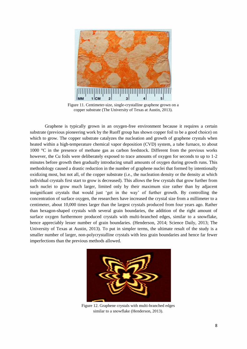
insignificant crystals that would just ‘get in the way’ of further growth. By controlling the
concentration of surface oxygen, the researchers have increased the crystal size from a millimeter to a
centimeter, about 10,000 times larger than the largest crystals produced from four years ago. Rather
than hexagon-shaped crystals with several grain boundaries, the addition of the right amount of
surface oxygen furthermore produced crystals with multi-branched edges, similar to a snowflake,
hence appreciably lesser number of grain boundaries. (Henderson, 2014; Science Daily, 2013; The
University of Texas at Austin, 2013). To put in simpler terms, the ultimate result of the study is a
smaller number of larger, non-polycrystalline crystals with less grain boundaries and hence far fewer
imperfections than the previous methods allowed.
Figure 11. Centimeter-size, single-crystalline graphene grown on a
copper substrate (The University of Texas at Austin, 2013).
Figure 12. Graphene crystals with multi-branched edges
similar to a snowflake (Henderson, 2013).

9
The simplicity of the method whereby graphene is just allowed to grow on a copper substrate
by deposition of methane at high temperatures and exposing it to oxygen at the right concentration is
as well remarkably beneficial than the much more complex steps (much like their complex names)
involved in micromechanical cleavage, epitaxial growth on SiC substrates, chemical reduction of
exfoliated graphene oxide, liquid phase exfoliation of graphite and unzipping of carbon nanotubes. In
addition, neither expensive acids nor any other harmful substances are involved in the process; it’s
just methane which is virtually harmless if properly contained and handled upon. This new method
essentially as well offers less wastes (only unutilized methane vapor) compared to other conventional
methods. This indeed is a step towards more economically-viable, cleaner and ‘greener’ ways of
mass-producing graphene (Graphenea, nd).
So what are the tangible benefits this study led the researchers to? From the crystals formed, a
major finding by the team was that the “carrier mobility” of electrons (how fast the electrons move) in
graphene films grown in the presence of surface oxygen is exceptionally high. This is important
because the speed at which the charge carriers move is important for many electronic devices – the
greater the speed, the faster the device can perform. Yufeng Hao deliberately says that the knowledge
gained in this study could prove useful to industry. For instance, these single-crystal films will
eventually allow existing devices to perform tasks quicker and more efficient and later be used as
prototype materials for the evaluation and development of new types of devices with superb features
than could be achieved before. This, undeniably, will be a huge leap in the field of electronics
(Science Daily, 2013).
Much for the results of the current research, the study enabled only the determination of the
effects of varying oxygen surface concentration to the electrical properties (and implicitly
optoelectrical and thermal properties) of the graphene crystals produced. The effect of such variable
on other promising graphene properties including the mechanical and chemical ones are yet to be
exploited or discovered. Moreover, extensive years and effort have yet to be undertaken and several
enduring tests have to be performed before graphene crystals can be enlarged to approximately meter
sizes. Nevertheless, the surface oxygen method of graphene production is an evidence that better
innovations are not impossible to materialize for the resolute, determined individuals equipped with
resourcefulness and the will to manifest such.
Figure 13. Comparison of Graphene grown on oxygen-rich copper (left) and oxygen-free
copper (right) (The University of Texas at Austin, 2013).
10
References
1. AzoNano, 2014. Graphene Oxide- Properties and Applications. Accessed March 5, 2014.
From http://www.azonano.com/article.aspx?ArticleID=2934.
2. Autosavant, 2008. Carbon Fiber for the Common Man. Accessed on March 1, 2014. From
http://www.autosavant.com/2008/05/28/carbon-fiber-for-the-common-man/.
3. Berger, M. 2013. Graphene: World-leading Research and Development. Accessed on
February 28, 2014. From http://www.nanotechnology/graphene/properties-uses-and-
applications/.
4. Brewster, S. 2013. What is graphene? Here’s what you need to know about a material that
could be the next silicon. Accessed on February 28, 2014. From
http://gigaom.com/2013/07/15/what-is-graphene-heres-what-you-need-to-know-about-a-
material-that-could-be-the-next-silicon/.
5. de la Fuente, J. nd. Graphene-What is it?. Accessed on February 28, 2014. From
http://www.graphenea.com/pages/graphene#.Uxa4n4ZBmMJ.
6. Graphene Supermarket, nd. Graphene-oxide paper. Accessed March 4, 2014. From
https://graphene-supermarket.com/Graphene-Oxide-Paper.html.
7. Graphenea, nd. CVD Graphene-Production Problems. Accessed March 1, 2014. From
http://www.cubashe.co.uk/cvd-graphene-production-problems/.
8. Guardian News and Media Limited, 2013. Graphene-the new wonder material. Accessed on
February 28, 2014. From http://www.theguardian.com/science/2013/nov/26/graphene-
molecule-potential-wonder-material.
9. Henderson, S. 2013. Surface Oxygen Proves Key to Growing XL Graphene Crystals.
Accessed March 1, 2014. From http://www.novuslight.com/surface-oxygen-proves-key-to-
growing-xl-graphene-crystals_N1917.html.
10. Hsu, C. 2012. Using Graphene, Scientists Develop a Less Toxic Way to Rust-Proof Steel.
Accessed on March 1, 2014. From
http://www.buffalo.edu/news/releases/2012/05/13401.html.
11. Laden, G. 2013. Graphene: Big promise for new solar technologies. Accessed on March 4,
2014. From http://scienceblogs.com/gregladen/2013/02/26/graphene-big-promise-for-new-
solar-technologies/.
12. Nano werk, 2012. Mass Production of high quality graphene: An analysis of worldwide
patents. Accessed on February 28,2014. From
http://www.nanowerk.com/spotlight/spotid=25744.php.

11
13. Plastic Electronics, 2012. Scientist develop conductive graphene-based material. Accessed on
March 1, 2014. From http://www.plusplasticelectronics.com/smartfabricstextiles/scientists-
develop-conductive-graphene-based-material-54588.aspx.
14. The University of Texas at Austin, 2013. Large Graphene Crystals With Exceptional
Electrical Properties Created. Science Daily.
15. The University of Austin at Texas, 2013. Ruoff Group Achieves Fundamental Understanding
of Graphene Growth. Accessed on February 28, 2014. From
http://www.me.utexas.edu/news/2013/1013_hao_ruoff_science.php.
16. The University of Austin at Texas, 2013. UT Austin Researchers Grow Large Graphene
Crystals That Have Exceptional Electrical Properties. Accessed on March 1, 2014. From
http://www.utexas.edu/news/2013/11/14/graphene-crystals-ut-researchers/.
17. Xtremevbtalk, 2014. Microsofts Wakeup Call: Console quality, cloud based game streaming.
Accessed on February 28, 2014. From www.xtremevbtalk.com.