Effect of surface morphology on friction of graphene on various substrates
7
Effect of surface morphology on friction of graphene on various substrates† Dae-Hyun Cho, ab Lei Wang, c Jin-Seon Kim, ab Gwan-Hyoung Lee, cd Eok Su Kim, e Sunhee Lee, e Sang Yoon Lee, e James Hone * c and Changgu Lee * af The friction of graphene on various substrates, such as SiO 2 , h-BN, bulk-like graphene, and mica, was investigated to characterize the adhesion level between graphene and the underlying surface. The friction of graphene on SiO 2 decreased with increasing thickness and converged around the penta- layers due to incomplete contact between the two surfaces. However, the friction of graphene on an atomically flat substrate, such as h-BN or bulk-like graphene, was low and comparable to that of bulk- like graphene. In contrast, the friction of graphene folded onto bulk-like graphene was indistinguishable from that of mono-layer graphene on SiO 2 despite the ultra-smoothness of bulk-like graphene. The characterization of the graphene's roughness before and after folding showed that the corrugation of graphene induced by SiO 2 morphology was preserved even after it was folded onto an atomically flat substrate. In addition, graphene deposited on mica, when folded, preserved the same corrugation level as before the folding event. Our friction measurements revealed that graphene, once exfoliated from the bulk crystal, tends to maintain its corrugation level even after it is folded onto an atomically flat substrate and that ultra-flatness in both graphene and the substrate is required to achieve the intimate contact necessary for strong adhesion. Since the rst isolation of graphene by micromechanical cleavage of graphite in 2004, 1 new electronic devices utilizing its extraordinary electronic properties have been envisioned. 2 However, the performance of graphene-based electronic devices fabricated on SiO 2 substrates is less than that predicted by theory, because carrier mobility is limited by the scattering from charged surfaces and impurities, 3,4 substrate surface rough- ness, 5–7 and surface optical phonons in SiO 2 . 8,9 Electron–hole puddles 10,11 and surface domains caused by ripple distortions on SiO 2 substrates 12 also limit the performance of graphene devices. For these reasons, the inuence of substrates on the electronic performance of graphene-based devices has been studied. 13–15 Recent studies have shown that high carrier mobility and charge homogeneity comparable to those of suspended graphene can be attained by fabricating graphene devices on h-BN. 16–18 Therefore, to improve the stacking technique used in fabricating graphene devices and device performance, a detailed study of the interfa- cial binding between graphene and the underlying substrate is required. If the interfacial binding force is insufficient, graphene can fold and bend along a kinked line of the substrate even by a weak shear force on the graphene surface, resulting in defects and functional groups. 19–21 As a result, a mechanical failure of the graphene-based device may occur at the interface, despite the unparalleled mechanical strength of graphene. 22 In relation, even a partial detachment of graphene from the substrate can lead to an electronic breakdown, as well as mechanical failure, because the electronic properties of folded graphene are quite different from those of at graphene. 23,24 Substrate morphology is one of the key factors inuencing the interfacial binding level. 25 A theoretical computation showed that the surface corrugation of graphene sitting on a substrate varies according to the substrate morphology. 26 On a corrugated substrate, the van der Waals interaction energy is minimized by conformation of the graphene sheet to the substrate morphology, at the price of increased elastic and bending energy. The nal morphology of the sheet is determined by the balance between these two terms, resulting in partial conformation of the graphene sheet to the substrate surface. 5 In other words, the contact intimacy between graphene and an underlying substrate is determined by substrate morphology and graphene stiffness. 25 a School of Mechanical Engineering, Sungkyunkwan University, 2066, Seobu-ro, Jangan-gu, Suwon, Gyeonggi, Republic of Korea. E-mail: [email protected] b Center for Integrated Nanostructure Physics (CINAP), Institute for Basic Science(IBS), Sungkyunkwan University, Korea c Department of Mechanical Engineering, Columbia University, New York, NY 10027, USA. E-mail: [email protected] d Samsung-SKKU Graphene Center (SSGC), Suwon 440-746, Republic of Korea e Display Device Laboratory, Samsung Advanced Institute of Technology, Samsung Electronics, Yongin, Gyeonggi 446-712, Republic of Korea f SKKU Advanced Institute of Nanotechnology, Sungkyunkwan University, 2066, Seobu- ro, Jangan-gu, Suwon, Gyeonggi, Republic of Korea † Electronic supplementary information (ESI) available: Sample preparation method, identication of graphene thickness, AFM and FFM measurements. See DOI: 10.1039/c3nr34181j Cite this: Nanoscale, 2013, 5, 3063 Received 19th December 2012 Accepted 8th February 2013 DOI: 10.1039/c3nr34181j www.rsc.org/nanoscale This journal is ª The Royal Society of Chemistry 2013 Nanoscale, 2013, 5, 3063–3069 | 3063 Nanoscale PAPER Published on 12 February 2013. Downloaded by Columbia University on 28/08/2014 05:47:30. View Article Online View Journal | View Issue
Transcript of Effect of surface morphology on friction of graphene on various substrates
Nanoscale
PAPER
Publ
ishe
d on
12
Febr
uary
201
3. D
ownl
oade
d by
Col
umbi
a U
nive
rsity
on
28/0
8/20
14 0
5:47
:30.
View Article OnlineView Journal | View Issue
aSchool of Mechanical Engineering, Sung
Jangan-gu, Suwon, Gyeonggi, Republic of KobCenter for Integrated Nanostructure Physics
Sungkyunkwan University, KoreacDepartment of Mechanical Engineering, Co
USA. E-mail: [email protected] Graphene Center (SSGC), SeDisplay Device Laboratory, Samsung Adva
Electronics, Yongin, Gyeonggi 446-712, RepufSKKU Advanced Institute of Nanotechnology
ro, Jangan-gu, Suwon, Gyeonggi, Republic o
† Electronic supplementary informationmethod, identication of graphene thicSee DOI: 10.1039/c3nr34181j
Cite this: Nanoscale, 2013, 5, 3063
Received 19th December 2012Accepted 8th February 2013
DOI: 10.1039/c3nr34181j
www.rsc.org/nanoscale
This journal is ª The Royal Society of
Effect of surface morphology on friction of graphene onvarious substrates†
Dae-Hyun Cho,ab Lei Wang,c Jin-Seon Kim,ab Gwan-Hyoung Lee,cd Eok Su Kim,e
Sunhee Lee,e Sang Yoon Lee,e James Hone*c and Changgu Lee*af
The friction of graphene on various substrates, such as SiO2, h-BN, bulk-like graphene, and mica, was
investigated to characterize the adhesion level between graphene and the underlying surface. The
friction of graphene on SiO2 decreased with increasing thickness and converged around the penta-
layers due to incomplete contact between the two surfaces. However, the friction of graphene on an
atomically flat substrate, such as h-BN or bulk-like graphene, was low and comparable to that of bulk-
like graphene. In contrast, the friction of graphene folded onto bulk-like graphene was
indistinguishable from that of mono-layer graphene on SiO2 despite the ultra-smoothness of bulk-like
graphene. The characterization of the graphene's roughness before and after folding showed that the
corrugation of graphene induced by SiO2 morphology was preserved even after it was folded onto an
atomically flat substrate. In addition, graphene deposited on mica, when folded, preserved the same
corrugation level as before the folding event. Our friction measurements revealed that graphene, once
exfoliated from the bulk crystal, tends to maintain its corrugation level even after it is folded onto an
atomically flat substrate and that ultra-flatness in both graphene and the substrate is required to
achieve the intimate contact necessary for strong adhesion.
Since the rst isolation of graphene by micromechanicalcleavage of graphite in 2004,1 new electronic devices utilizing itsextraordinary electronic properties have been envisioned.2
However, the performance of graphene-based electronic devicesfabricated on SiO2 substrates is less than that predicted bytheory, because carrier mobility is limited by the scattering fromcharged surfaces and impurities,3,4 substrate surface rough-ness,5–7 and surface optical phonons in SiO2.8,9 Electron–holepuddles10,11 and surface domains caused by ripple distortions onSiO2 substrates12 also limit the performance of graphene devices.For these reasons, the inuence of substrates on the electronicperformance of graphene-based devices has been studied.13–15
Recent studies have shown that high carrier mobility and charge
kyunkwan University, 2066, Seobu-ro,
rea. E-mail: [email protected]
(CINAP), Institute for Basic Science(IBS),
lumbia University, New York, NY 10027,
uwon 440-746, Republic of Korea
nced Institute of Technology, Samsung
blic of Korea
, Sungkyunkwan University, 2066, Seobu-
f Korea
(ESI) available: Sample preparationkness, AFM and FFM measurements.
Chemistry 2013
homogeneity comparable to those of suspended graphene canbeattained by fabricating graphene devices on h-BN.16–18 Therefore,to improve the stacking technique used in fabricating graphenedevices and device performance, a detailed study of the interfa-cial binding between graphene and the underlying substrate isrequired. If the interfacial binding force is insufficient, graphenecan fold and bend along a kinked line of the substrate even by aweak shear force on the graphene surface, resulting in defectsand functional groups.19–21As a result, amechanical failure of thegraphene-based device may occur at the interface, despite theunparalleled mechanical strength of graphene.22 In relation,even a partial detachment of graphene from the substrate canlead to an electronic breakdown, as well as mechanical failure,because the electronic properties of folded graphene are quitedifferent from those of at graphene.23,24
Substratemorphology is one of the key factors inuencing theinterfacial binding level.25 A theoretical computation showedthat the surface corrugation of graphene sitting on a substratevaries according to the substrate morphology.26 On a corrugatedsubstrate, the van der Waals interaction energy is minimized byconformation of the graphene sheet to the substratemorphology, at theprice of increased elastic andbending energy.The nal morphology of the sheet is determined by the balancebetween these two terms, resulting inpartial conformation of thegraphene sheet to the substrate surface.5 In other words, thecontact intimacy between graphene and an underlying substrateis determinedby substratemorphology and graphene stiffness.25
Nanoscale, 2013, 5, 3063–3069 | 3063
Nanoscale Paper
Publ
ishe
d on
12
Febr
uary
201
3. D
ownl
oade
d by
Col
umbi
a U
nive
rsity
on
28/0
8/20
14 0
5:47
:30.
View Article Online
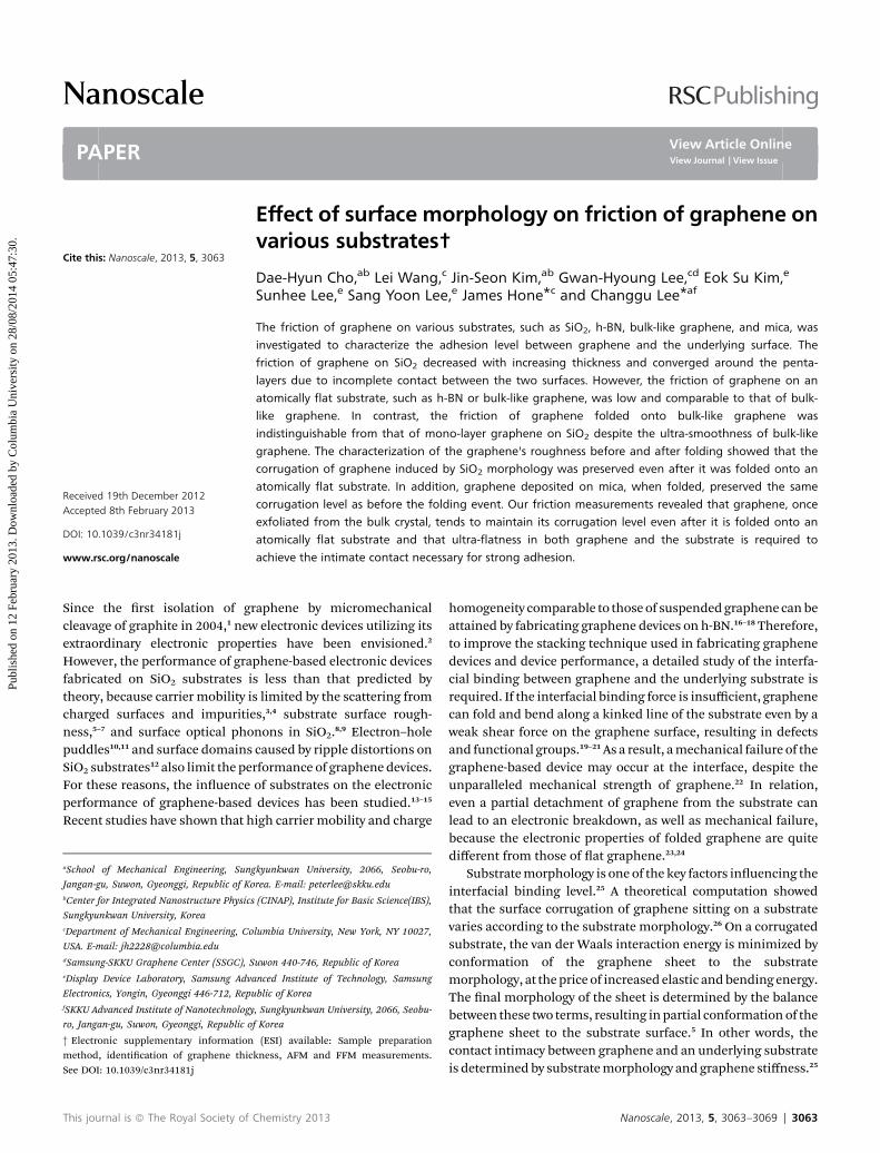
In addition, if graphene is corrugated prior to transfer, itmay notmake a conformal contact with an ultraat substrate. Whengraphene that was grown on a rough copper substrate bychemical vapor deposition was transferred onto a smoothersurface, it preserved its corrugated surface.27 Therefore, whencorrugated graphene is transferred onto an ultraat substrate, itmay adhere weakly to the substrate. In this context, we experi-mentally investigated the effects of surface morphology andcontact intimacy on graphene adhesion with various substratesby friction force microscopy (FFM) techniques. Our study notonly showed the effects of substratemorphology on the frictionalproperties of graphene but also suggested a new strategy fordetermining the binding strength between graphene and anunderlying substrate, especially between two 2-dimensional (2D)materials, by friction measurements.
In this study, we prepared graphene samples, where exfoli-ated graphene akes were placed on various substrates withdifferent surface morphologies: graphene on SiO2, graphene onh-BN, graphene on bulk-like graphene, folded graphene on SiO2,and folded graphene on mica. Here, ‘bulk-like graphene’ indi-cates graphenewithmore than 10 layers, thus having an ultraatsurface and the same physical properties as graphite. To preparethe ultraat substrates for graphene on h-BN and on bulk-likegraphene, we rst exfoliated thick h-BN and bulk-like graphenefrom a bulk source on a silicon substrate with a capping layer of300 nm SiO2 by the mechanical cleavage method (see ESI†).Then, to avoid any contamination, we deposited graphene ontothe already exfoliated thick h-BN and bulk-like graphenesubstrates, as shown inFig. 1(a). The stacked graphene/h-BNandgraphene/bulk-like graphene were examined under an opticalmicroscope. For graphene on SiO2, graphene was also placed ona 300 nm thick SiO2 substrate right beside stacked graphene.Because the samples used in this study were not exposed to anysolvent or polymers,28 they were fairly clean enough for precisesurface investigation without concern of contamination. Forfolded graphene on SiO2 and folded graphene on mica, the fol-ded graphene samples were fabricated by scratching with anultrasharp diamond-like carbon (DLC) atomic force microscopy(AFM) tip (NT-MDT, NSG01, tip curvature radius R ¼ 1 to 3 nm)
Fig. 1 Schematics of sample preparation and friction measurements. (a) Gra-phene, both on ultraflat substrates (h-BN or bulk-like graphene) and SiO2, and (b)folded graphene on bulk-like graphene.
3064 | Nanoscale, 2013, 5, 3063–3069
against the edges of the graphene deposited on SiO2 and mica(Fig. 1(b)).29 The number of graphene layers was identied byoptical microscopy and Raman spectroscopy.30 All the sampleswere then scanned by contact-mode AFM with a sharp Si tip(Seiko, SI-AF01, tip curvature radius R ¼ 10 nm) to measure thefriction distribution at different areas with an applied load of 1nN. Every test was done in an ambient environment (25 to 50%relative humidity, 20 to 25 �C). A friction force exerted at the apexof the AFM tip during scanning will cause the cantilever to twistin the frictionmode of AFM.The angle difference of the deectedlaser beam can be detected by the photodetector. Therefore,without lateral force calibration of the AFM cantilever, the fric-tion signals taken from different areas can be simultaneouslyprocessed and compared to evaluate the interaction betweengraphene and the substrate.31
Fig. 2 shows the friction behavior of graphene according tothe substrate (h-BN, bulk-like graphene, and SiO2). In Fig. 2(a)–(c), the frictionbehaviors ofmono-, bi-, andpenta-layer grapheneon h-BN are contrasted with those of graphene on SiO2 of cor-responding thickness and in Fig. 2(d)–(f), the friction behaviorsofmono-, bi-, and hexa-layer graphene on bulk-like graphene arecontrasted with those of graphene on SiO2 of correspondingthickness. In the friction images of mono- and bi-layer graphene(Fig. 2(a), (b), (d) and (e)), the friction behaviors vary dependingon the type of supporting material, and the graphene akes onultraat substrates (graphene on h-BN and graphene on bulk-like graphene) exhibit lower friction force than the grapheneakes on SiO2. However, thicker graphene (penta- and hexa-layers) showed almost negligible difference in the frictionbehavior between the two regions as shown in Fig. 2(c) and (f). Inan additional friction test that was performed for graphene withmono- and tri-layers adjoining each other on a piece of h-BN(Fig. 3(a)), there was no difference in friction force betweenmono- and tri-layer graphene (Fig. 3(b)). We observed a similarfriction behavior in bi-layer graphene on bulk-like graphene(Fig. 3(c) and (d)). Therefore, it is evident that the frictionbehavior of graphene onh-BNor graphene onbulk-like grapheneis not dependent on graphene thickness because of the ultra-atness of the corresponding substrate and sufficient adhesion.
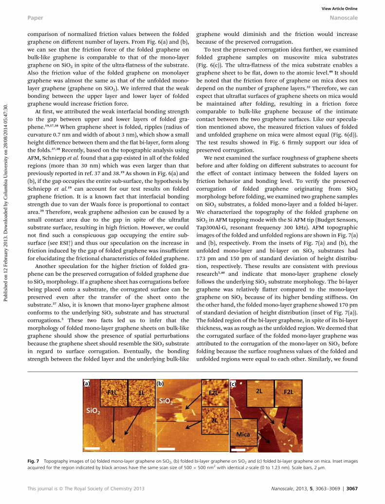
We quantied the differences of the friction forces amongdifferent areas of various substrates by subtracting backwardscan friction values from forward scan friction values, and thennormalizing the friction of graphene on SiO2 by that of gra-phene on atomically at substrates (h-BN or bulk-like gra-phene). Fig. 4 shows the normalized friction signals accordingto the number of layers. An identical trend of decreasing frictionof graphene with increasing number of layers up to penta-layerswas observed for the SiO2 substrate, as shown in both Fig. 4(a)and (b). The thickness dependence of friction on SiO2 in ourstudy has a similar trend to previous observations.32–34 AlthoughFilleter et al.33 and Lee et al.34 argued that the thicknessdependence would be due to phonon–electron coupling ingraphene or van der Waals interaction between the AFM tip andgraphene, recent observations strongly suggest that puckeringof graphene derived from low bending stiffness of an atomicallythin graphene sheet is the main cause of thisphenomenon.12,32,35
This journal is ª The Royal Society of Chemistry 2013
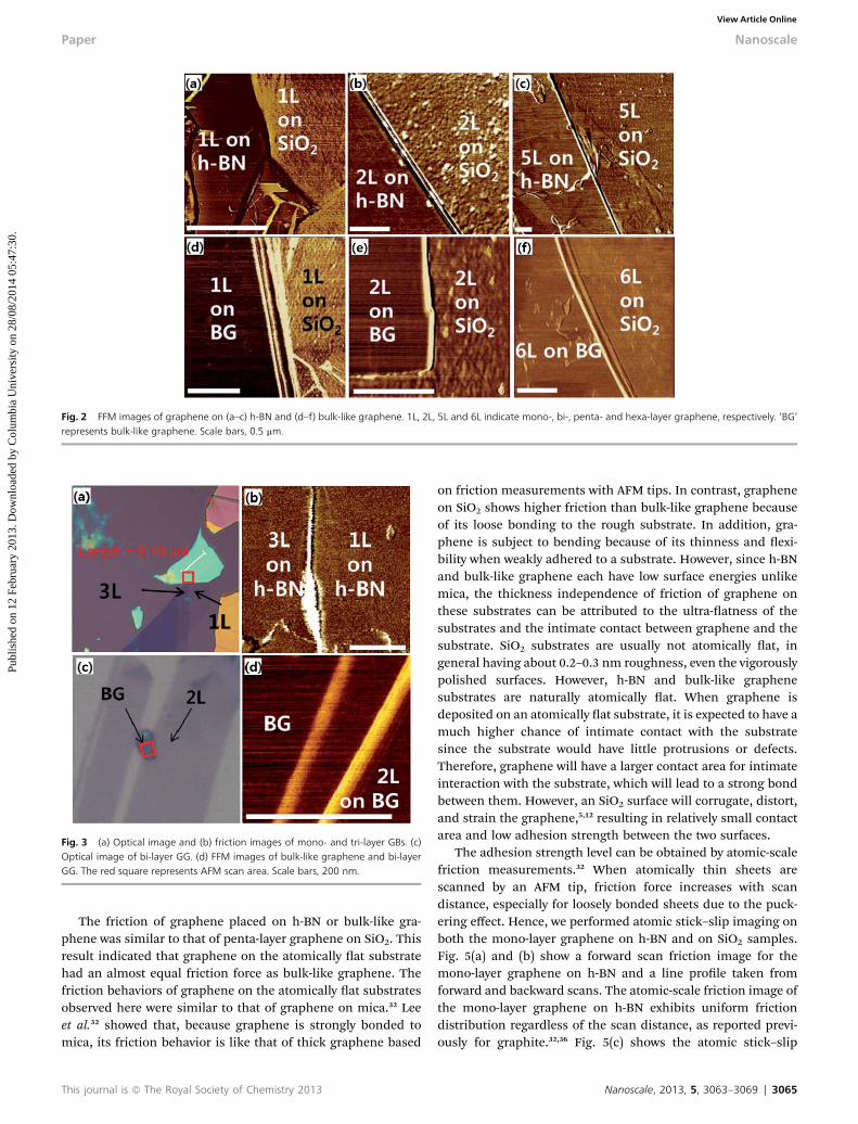
Fig. 2 FFM images of graphene on (a–c) h-BN and (d–f) bulk-like graphene. 1L, 2L, 5L and 6L indicate mono-, bi-, penta- and hexa-layer graphene, respectively. ‘BG’represents bulk-like graphene. Scale bars, 0.5 mm.
Fig. 3 (a) Optical image and (b) friction images of mono- and tri-layer GBs. (c)Optical image of bi-layer GG. (d) FFM images of bulk-like graphene and bi-layerGG. The red square represents AFM scan area. Scale bars, 200 nm.
Paper Nanoscale
Publ
ishe
d on
12
Febr
uary
201
3. D
ownl
oade
d by
Col
umbi
a U
nive
rsity
on
28/0
8/20
14 0
5:47
:30.
View Article Online
The friction of graphene placed on h-BN or bulk-like gra-phene was similar to that of penta-layer graphene on SiO2. Thisresult indicated that graphene on the atomically at substratehad an almost equal friction force as bulk-like graphene. Thefriction behaviors of graphene on the atomically at substratesobserved here were similar to that of graphene on mica.32 Leeet al.32 showed that, because graphene is strongly bonded tomica, its friction behavior is like that of thick graphene based
This journal is ª The Royal Society of Chemistry 2013
on friction measurements with AFM tips. In contrast, grapheneon SiO2 shows higher friction than bulk-like graphene becauseof its loose bonding to the rough substrate. In addition, gra-phene is subject to bending because of its thinness and exi-bility when weakly adhered to a substrate. However, since h-BNand bulk-like graphene each have low surface energies unlikemica, the thickness independence of friction of graphene onthese substrates can be attributed to the ultra-atness of thesubstrates and the intimate contact between graphene and thesubstrate. SiO2 substrates are usually not atomically at, ingeneral having about 0.2–0.3 nm roughness, even the vigorouslypolished surfaces. However, h-BN and bulk-like graphenesubstrates are naturally atomically at. When graphene isdeposited on an atomically at substrate, it is expected to have amuch higher chance of intimate contact with the substratesince the substrate would have little protrusions or defects.Therefore, graphene will have a larger contact area for intimateinteraction with the substrate, which will lead to a strong bondbetween them. However, an SiO2 surface will corrugate, distort,and strain the graphene,5,12 resulting in relatively small contactarea and low adhesion strength between the two surfaces.
The adhesion strength level can be obtained by atomic-scalefriction measurements.32 When atomically thin sheets arescanned by an AFM tip, friction force increases with scandistance, especially for loosely bonded sheets due to the puck-ering effect. Hence, we performed atomic stick–slip imaging onboth the mono-layer graphene on h-BN and on SiO2 samples.Fig. 5(a) and (b) show a forward scan friction image for themono-layer graphene on h-BN and a line prole taken fromforward and backward scans. The atomic-scale friction image ofthe mono-layer graphene on h-BN exhibits uniform frictiondistribution regardless of the scan distance, as reported previ-ously for graphite.32,36 Fig. 5(c) shows the atomic stick–slip
Nanoscale, 2013, 5, 3063–3069 | 3065
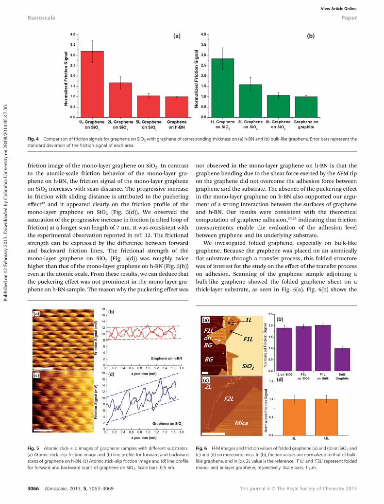
Fig. 4 Comparison of friction signals for graphene on SiO2 with graphene of corresponding thickness on (a) h-BN and (b) bulk-like graphene. Error bars represent thestandard deviation of the friction signal of each area.
Nanoscale Paper
Publ
ishe
d on
12
Febr
uary
201
3. D
ownl
oade
d by
Col
umbi
a U
nive
rsity
on
28/0
8/20
14 0
5:47
:30.
View Article Online
friction image of the mono-layer graphene on SiO2. In contrastto the atomic-scale friction behavior of the mono-layer gra-phene on h-BN, the friction signal of the mono-layer grapheneon SiO2 increases with scan distance. The progressive increasein friction with sliding distance is attributed to the puckeringeffect32 and it appeared clearly on the friction prole of themono-layer graphene on SiO2 (Fig. 5(d)). We observed thesaturation of the progressive increase in friction (a tilted loop offriction) at a longer scan length of 7 nm. It was consistent withthe experimental observation reported in ref. 32. The frictionalstrength can be expressed by the difference between forwardand backward friction lines. The frictional strength of themono-layer graphene on SiO2 (Fig. 5(d)) was roughly twicehigher than that of the mono-layer graphene on h-BN (Fig. 5(b))even at the atomic-scale. From these results, we can deduce thatthe puckering effect was not prominent in the mono-layer gra-phene on h-BN sample. The reason why the puckering effect was
Fig. 5 Atomic stick–slip images of graphene samples with different substrates.(a) Atomic stick–slip friction image and (b) line profile for forward and backwardscans of graphene on h-BN. (c) Atomic stick–slip friction image and (d) line profilefor forward and backward scans of graphene on SiO2. Scale bars, 0.5 nm.
3066 | Nanoscale, 2013, 5, 3063–3069
not observed in the mono-layer graphene on h-BN is that thegraphene bending due to the shear force exerted by the AFM tipon the graphene did not overcome the adhesion force betweengraphene and the substrate. The absence of the puckering effectin the mono-layer graphene on h-BN also supported our argu-ment of a strong interaction between the surfaces of grapheneand h-BN. Our results were consistent with the theoreticalcomputation of graphene adhesion,25,26 indicating that frictionmeasurements enable the evaluation of the adhesion levelbetween graphene and its underlying substrate.
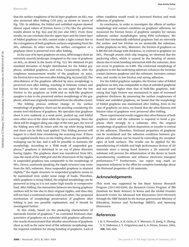
We investigated folded graphene, especially on bulk-likegraphene. Because the graphene was placed on an atomicallyat substrate through a transfer process, this folded structurewas of interest for the study on the effect of the transfer processon adhesion. Scanning of the graphene sample adjoining abulk-like graphene showed the folded graphene sheet on athick-layer substrate, as seen in Fig. 6(a). Fig. 6(b) shows the
Fig. 6 FFM images and friction values of folded graphene (a) and (b) on SiO2 and(c) and (d) on muscovite mica. In (b), friction values are normalized to that of bulk-like graphene, and in (d), 2L value is the reference. ‘F1L’ and ‘F2L’ represent foldedmono- and bi-layer graphene, respectively. Scale bars, 1 mm.
This journal is ª The Royal Society of Chemistry 2013
Paper Nanoscale
Publ
ishe
d on
12
Febr
uary
201
3. D
ownl
oade
d by
Col
umbi
a U
nive
rsity
on
28/0
8/20
14 0
5:47
:30.
View Article Online
comparison of normalized friction values between the foldedgraphene on different number of layers. From Fig. 6(a) and (b),we can see that the friction force of the folded graphene onbulk-like graphene is comparable to that of the mono-layergraphene on SiO2 in spite of the ultra-atness of the substrate.Also the friction value of the folded graphene on monolayergraphene was almost the same as that of the unfolded mono-layer graphene (graphene on SiO2). We inferred that the weakbonding between the upper layer and lower layer of foldedgraphene would increase friction force.
At rst, we attributed the weak interfacial bonding strengthto the gap between upper and lower layers of folded gra-phene.19,37,38 When graphene sheet is folded, ripples (radius ofcurvature 0.7 nm and width of about 3 nm), which show a smallheight difference between them and the at bi-layer, form alongthe folds.37,38 Recently, based on the topographic analysis usingAFM, Schniepp et al. found that a gap existed in all of the foldedregions (more than 30 nm) which was even larger than thatpreviously reported in ref. 37 and 38.19 As shown in Fig. 6(a) and(b), if the gap occupies the entire sub-surface, the hypothesis bySchniepp et al.19 can account for our test results on foldedgraphene friction. It is a known fact that interfacial bondingstrength due to van der Waals force is proportional to contactarea.39 Therefore, weak graphene adhesion can be caused by asmall contact area due to the gap in spite of the ultraatsubstrate surface, resulting in high friction. However, we couldnot nd such a conspicuous gap occupying the entire sub-surface (see ESI†) and thus our speculation on the increase infriction induced by the gap of folded graphene was insufficientfor elucidating the frictional characteristics of folded graphene.
Another speculation for the higher friction of folded gra-phene can be the preserved corrugation of folded graphene dueto SiO2 morphology. If a graphene sheet has corrugations beforebeing placed onto a substrate, the corrugated surface can bepreserved even aer the transfer of the sheet onto thesubstrate.27 Also, it is known that mono-layer graphene almostconforms to the underlying SiO2 substrate and has structuralcorrugations.5 These two facts led us to infer that themorphology of folded mono-layer graphene sheets on bulk-likegraphene should show the presence of spatial perturbationsbecause the graphene sheet should resemble the SiO2 substratein regard to surface corrugation. Eventually, the bondingstrength between the folded layer and the underlying bulk-like
Fig. 7 Topography images of (a) folded mono-layer graphene on SiO2, (b) foldedacquired for the region indicated by black arrows have the same scan size of 500 �
This journal is ª The Royal Society of Chemistry 2013
graphene would diminish and the friction would increasebecause of the preserved corrugation.
To test the preserved corrugation idea further, we examinedfolded graphene samples on muscovite mica substrates(Fig. 6(c)). The ultra-atness of the mica substrate enables agraphene sheet to be at, down to the atomic level.40 It shouldbe noted that the friction force of graphene on mica does notdepend on the number of graphene layers.32 Therefore, we canexpect that ultraat surfaces of graphene sheets on mica wouldbe maintained aer folding, resulting in a friction forcecomparable to bulk-like graphene because of the intimatecontact between the two graphene surfaces. Like our specula-tion mentioned above, the measured friction values of foldedand unfolded graphene on mica were almost equal (Fig. 6(d)).The test results showed in Fig. 6 rmly support our idea ofpreserved corrugation.
We next examined the surface roughness of graphene sheetsbefore and aer folding on different substrates to account forthe effect of contact intimacy between the folded layers onfriction behavior and bonding level. To verify the preservedcorrugation of folded graphene originating from SiO2
morphology before folding, we examined two graphene sampleson SiO2 substrates, a folded mono-layer and a folded bi-layer.We characterized the topography of the folded graphene onSiO2 in AFM tapping mode with the Si AFM tip (Budget Sensors,Tap300Al-G, resonant frequency 300 kHz). AFM topographicimages of the folded and unfolded regions are shown in Fig. 7(a)and (b), respectively. From the insets of Fig. 7(a) and (b), theunfolded mono-layer and bi-layer on SiO2 substrates had173 pm and 150 pm of standard deviation of height distribu-tion, respectively. These results are consistent with previousresearch5,40 and indicate that mono-layer graphene closelyfollows the underlying SiO2 substrate morphology. The bi-layergraphene was relatively atter compared to the mono-layergraphene on SiO2 because of its higher bending stiffness. Onthe other hand, the foldedmono-layer graphene showed 170 pmof standard deviation of height distribution (inset of Fig. 7(a)).The folded region of the bi-layer graphene, in spite of its bi-layerthickness, was as rough as the unfolded region. We deemed thatthe corrugated surface of the folded mono-layer graphene wasattributed to the corrugation of the mono-layer on SiO2 beforefolding because the surface roughness values of the folded andunfolded regions were equal to each other. Similarly, we found
bi-layer graphene on SiO2 and (c) folded bi-layer graphene on mica. Inset images500 nm2 with identical z-scale (0 to 1.23 nm). Scale bars, 2 mm.
Nanoscale, 2013, 5, 3063–3069 | 3067
Nanoscale Paper
Publ
ishe
d on
12
Febr
uary
201
3. D
ownl
oade
d by
Col
umbi
a U
nive
rsity
on
28/0
8/20
14 0
5:47
:30.
View Article Online
that the surface roughness of the bi-layer graphene on SiO2 wasalso preserved aer folding (150 pm), as shown in insets ofFig. 7(b). In addition, the folded and unfolded regions showedalmost equal values of friction forces (�5%) like the previousresults shown in Fig. 6(a) and (b) (see also ESI†). From theseresults, we can conclude that the upper layer and the lower layerof folded graphene on SiO2 cannot make a tight contact due tothe corrugations of both graphene surfaces originating from theSiO2 substrate. In other words, the surface corrugation of agraphene sheet is preserved even aer folding.
In the case of bi-layer graphene onmica, AFM images show anextremely smooth landscape compared to the case of grapheneon SiO2, as shown in the insets of Fig. 7(c). We obtained 89 pmstandard deviation of height distribution for the folded gra-phene, unfolded graphene, and mica. Consistently, with theroughness measurement results of the graphene on mica,the friction forcewas low evenaer folding (Fig. 6(c) and (d)). Theultra-atness of the graphene affected by mica morphology ispreserved even aer folding, resulting in intimate contact andlow friction. In the same context, we can argue that the lowfriction in the graphene on h-BN and on bulk-like graphenesamples is due to the preserved surface morphology of the gra-phene,whichwasoriginally transferred from theultraat crystal.
The folding process without change in the surfacemorphology of graphene sheet can be puzzling considering theatomic level thickness of graphene. We speculate that graphenesheet is torn suddenly at a weak point, pushed up, and foldedonto other area of the sheet while the tip is scanning. Since thesheet will be dragged along one edge of the torn part, the rest ofthe folding area will be intact with the tip while being foldedand there can be little load applied. This folding process willhappen in a short time considering the scanning time. If thereis no applied tensile force on the folding sheet, the possibility ofreshaping can be low, and it will be possible to maintain themorphology. According to a TEM study of suspended gra-phene,41 graphene is deformed in an out of plane directionhaving ripples. The graphene sheet was transferred from SiO2
onto the mesh of the TEM grid and the dimension of the ripplesin suspended graphene was comparable to the morphology ofSiO2. Hence, cautiously speaking, the ripple structure may comefrom the SiO2 substrate. Since suspended graphene is strainedslightly,22 the ripple structure in suspended graphene seems tobe maintained even under some range of loads. Therefore,while graphene is being folded, the original morphology can bepreserved as long as it is not under high tensile or compressiveload. Aer folding, the interaction between two facing graphenesurfaces will be low due to their original ripples, and thus theywill not have a conformal contact with each other. Our proposedmechanism of morphology preservation of graphene aerfolding is just one possible explanation, and it should beinvestigated further.
In this study, based on the puckering characteristic ofnanoscale friction of graphene,32 we correlated frictional char-acteristics of graphene on a substrate with graphene adhesion.Our results demonstrated that ultraat smoothness of graphenesheet as well as the same level of at substrate morphology wasthe required condition for strong bonding of graphene. Lack of
3068 | Nanoscale, 2013, 5, 3063–3069
either condition would result in increased friction and weakadhesion of graphene.
In conclusion, in order to investigate the effects of surfacemorphology and contact condition on graphene adhesion, wemeasured the friction forces of graphene samples for varioussubstrate surface morphologies using FFM techniques. Wefound that mechanically exfoliated graphene had an extremelyat surface and low friction on an atomically at substrate,unlike graphene on SiO2. Moreover, the friction of graphene onh-BN did not change with thickness, in contrast to graphene onSiO2. Through atomic stick–slip imaging, we observed that thepuckering effect, which is caused by the bending of atomicsheets due to weak bonding interaction with the substrate, doesnot occur in graphene on h-BN. The conformal morphology ofgraphene to the at underlying substrate enhances the intimatecontact between graphene and the substrate, increases contactarea, and results in low friction and strong adhesion.
For the folded graphene samples, the friction value of foldedgraphene on SiO2 was comparable to that of unfolded grapheneand was much higher than that of bulk-like graphene, indi-cating that high friction was maintained in spite of increasedgraphene thickness. By measuring the surface roughnesses offolded and unfolded graphene, we found that the morphologyof folded graphene was maintained aer folding. Even in thecase of graphene on mica, we found that the ultra-atness andfriction value of graphene were preserved aer folding.
These experimental results suggest that ultra-atness of bothgraphene sheet and the substrate is required to bond a gra-phene sheet strongly to a substrate. Also, the originalmorphology of graphene before deposition or transfer is criticalto the adhesion. Therefore, frictional properties of graphenecan be modulated and the adhesion condition between gra-phene and substrate can be tuned by controlling the morphol-ogies of both surfaces. The results can be applied for themanufacturing of reliable and high performance devices of 2Dmaterials since a strong bond between a 2D material andsubstrate will prevent the delamination of the device in harshmanufacturing conditions and enhance electronic transportperformance.16–18 Furthermore, our report may mark animportant milestone in the effort for complete knowledge aboutthe frictional properties of 2D materials.
Acknowledgements
This work was supported by the Basic Science ResearchProgram (2011-0014209), the Research Center Program of IBS(Institute for Basic Science) in Korea and the Global FrontierResearch Center for Advanced So Electronics (2011-0031629)through the NRF funded by the Korean government Ministry ofEducation, Science and Technology (MEST), and SamsungElectronics.
References
1 K. S. Novoselov, A. K. Geim, S. V. Morozov, D. Jiang, Y. Zhang,S. V. Dubonos, I. V. Grigorieva and A. A. Firsov, Science, 2004,306, 666–669.
This journal is ª The Royal Society of Chemistry 2013
Paper Nanoscale
Publ
ishe
d on
12
Febr
uary
201
3. D
ownl
oade
d by
Col
umbi
a U
nive
rsity
on
28/0
8/20
14 0
5:47
:30.
View Article Online
2 Y. Lee, S. Bae, H. Jang, S. Jang, S.-E. Zhu, S. H. Sim, Y. I. Song,B. H. Hong and J.-H. Ahn, Nano Lett., 2010, 10, 490–493.
3 T. J. Ando, J. Phys. Soc. Jpn., 2006, 75, 074716.4 K. Nomura and A. H. MacDonald, Phys. Rev. Lett., 2007, 98,076602.
5 M. Ishigami, J. H. Chen, W. G. Cullen, M. S. Fuhrer andE. D. Williams, Nano Lett., 2007, 7, 1643–1648.
6 M. I. Katsnelson and A. K. Geim, Philos. Trans. R. Soc., A,2007, 366, 195–204.
7 S. V. Morozov, K. S. Novoselov, M. I. Katsnelson, F. Schedin,D. C. Elias, J. A. Jaszczak and A. K. Geim, Phys. Rev. Lett.,2008, 100, 016602.
8 S. Fratini and F. Guinea, Phys. Rev. B: Condens. Matter Mater.Phys., 2008, 77, 195415.
9 J.-H. Chen, C. Jang, S. Xiao, M. Ishigami and M. S. Fuhrer,Nat. Nanotechnol., 2008, 3, 206–209.
10 E. H. Hwang, S. Adam and S. Das Sarma, Phys. Rev. Lett.,2007, 98, 186806.
11 Y.-W. Tan, Y. Zhang, K. Bolotin, Y. Zhao, S. Adam,E. H. Hwang, S. Das Sarma, H. L. Stormer and P. Kim,Phys. Rev. Lett., 2007, 99, 246803.
12 J. S. Choi, J.-S. Kim, I.-S. Byun, D. H. Lee, M. J. Lee, B. H. Park,C. Lee, D. Yoon, H. Cheong, K. H. Lee, Y. –W. Son, J. Y. Parkand M. Salmeron, Science, 2011, 333, 607–610.
13 S. Y. Zhou, G.-H. Gweon, A. V. Fedrov, P. N. First, W. A. deHeer, D.-H. Lee, F. Guinea, A. H. Castro Neto andA. Lanzara, Nat. Mater., 2007, 6, 770–775.
14 T. O. Wehling, A. I. Lichtenstein and M. I. Katsnelson, Appl.Phys. Lett., 2008, 93, 202110.
15 X. Li, B. D. Kong, J. M. Zavada and K. W. Kim, Appl. Phys.Lett., 2011, 99, 233114.
16 C. R. Dean, A. F. Young, I. Meric, C. Lee, L. Wang,S. Sorgenfrei, K. Watanabe, T. Taniguchi, P. Kim,K. L. Shepard and J. Hone, Nat. Nanotechnol., 2010, 5, 722–726.
17 I. Meric, C. R. Dean, A. F. Young, J. Hone, P. Kim andK. L. Shepard, IEEE IEDM Tech. Dig., 2010, pp. 556–559.
18 R. Decker, Y. Wang, V. W. Brar, W. Regan, H.-Z. Tsai, Q. Wu,W. Gannett, A. Zettl andM. F. Crommie, Nano Lett., 2011, 11,2291–2295.
19 H. C. Schniepp, K. N. Kudin, J.-L. Li, R. K. Prud'homme,R. Car, D. A. Saville and I. A. Aksay, ACS Nano, 2008, 2,2577–2584.
20 V. Carozo, C. M. Almeida, E. H. M. Ferreira, L. G. Cancado,C. A. Achete and A. Jorio, Nano Lett., 2011, 11, 4527–4534.
This journal is ª The Royal Society of Chemistry 2013
21 K. S. Kim, H.-J. Lee, C. Lee, S.-K. Lee, H. Jang, J.-H. Ahn,J.-H. Kim and H.-J. Lee, ACS Nano, 2011, 5, 5107–5114.
22 C. Lee, X. Wei, J. W. Kysar and J. Hone, Science, 2008, 321,385–388.
23 J. M. B. Lopes dos Santos, N. M. R. Peres and A. H. CastroNeto, Phys. Rev. Lett., 2007, 99, 256802.
24 Z. Ni, Y. Wang, T. Yu, Y. You and Z. Shen, Phys. Rev. B:Condens. Matter Mater. Phys., 2008, 77, 235403.
25 J. S. Bunch and M. L. Dunn, Solid State Commun., 2012, 152,1359–1364.
26 W. Gao and R. Huang, J. Phys. D: Appl. Phys., 2011, 44,452001.
27 G. H. Han, F. Gunes, J. J. Bae, E. S. Kim, S. J. Chae, H.-J. Shin,J.-Y. Choi, D. Pribat and Y. H. Lee, Nano Lett., 2011, 11, 4144–4148.
28 G. H. Han, H.-J. Shin, E. S. Kim, S. J. Chae, J.-Y. Choi andY. H. Lee, NANO, 2011, 6, 59–65.
29 L. X. Li, R. P. Liu, Z. W. Chen, Q. Wang, M. Z. Ma, Q. Jing,G. Li and Y. Tian, Carbon, 2006, 44, 1544–1547.
30 A. C. Ferrari, J. C. Meyer, V. Scardaci, C. Casiraghi,M. Lazzeri, F. Mauri, S. Piscanec, D. Jiang, K. S. Novoselov,S. Roth and A. K. Geim, Phys. Rev. Lett., 2006, 97, 187401.
31 M. L. Palacio and B. Bhushan, Crit. Rev. Solid State Mater.Sci., 2010, 35, 73–104.
32 C. Lee, Q. Li, W. Kalb, X.-Z. Liu, H. Berger, R. W. Carpick andJ. Hone, Science, 2010, 328, 76–80.
33 T. Filleter, J. L. McChesney, A. Bostwick, E. Rotenberg,K. V. Emtsev, Th. Seyller, K. Horn and R. Bennewitz, Phys.Rev. Lett., 2009, 102, 086102.
34 H. Lee, N. Lee, J. Eom and S. Lee, Nanotechnology, 2009, 20,325701.
35 S. Kwon, J.-H. Ko, K.-J. Jeon, Y.-H. Kim and J. Y. Park, NanoLett., 2012, 12, 6043–6048.
36 J.-A. Ruan and B. Bhushan, J. Appl. Phys., 1994, 76, 5022–5035.
37 H. Hiura, T. W. Ebbesen, J. Fujita, K. Tanigaki andT. Takada, Nature, 1994, 367, 148–151.
38 A. K. Gupta, C. Nisoli, P. E. Lammert, V. H. Crespi andP. C. Eklund, J. Phys.: Condens. Matter, 2010, 22, 334205.
39 T. H. Fang, W. J. Chang and Y. C. Fan, NANO, 2010, 5, 231–236.
40 C. H. Lui, L. Liu, K. F. Mak, G. W. Flynn and T. F. Heinz,Nature, 2009, 462, 339–341.
41 J. C. Meyer, A. K. Geim, M. I. Katsnelson, K. S. Novoselov,T. J. Booth and S. Rogh, Nature, 2006, 446, 60–63.
Nanoscale, 2013, 5, 3063–3069 | 3069