Metallic and Non-Metallic Jewelery from the renewed excavations at Tell Beth Shean
Upload
independentCategory
view
3download
0
Scanning Tunneling Spectroscopic Studies of the Effects of Dielectrics and Metallic Substrates on the Local Electronic Characteristics of Graphene
N.-C. Yeha, M.-L. Teaguea, D. A. Boydb, M. W. Bockrathb,c, J. Velascoc, and C.-N. Lauc
a Department of Physics, California Institute of Technology, Pasadena, California 91125,
USA b Department of Applied Physics, California Institute of Technology, Pasadena,
California 91125, USA c Department of Physics, University of California, Riverside, California 92521, USA
Atomically resolved imaging and spectroscopic characteristics of graphene grown by chemical vapor deposition (CVD) on copper foils are investigated and compared with those of mechanical exfoliated graphene on SiO2. For exfoliated graphene, the local spectral deviations from ideal behavior may be attributed to strain induced by the SiO2 substrate. For CVD grown graphene, the lattice structure appears strongly distorted by the underlying copper, with regions in direct contact with copper showing nearly square lattices whereas suspended regions from thermal relaxation exhibiting nearly honeycomb or hexagonal lattice structures. The electronic density of states (DOS) correlates closely with the atomic arrangements of carbon, showing excess zero-bias tunneling conductance and nearly energy-independent DOS for strongly distorted graphene, in contrast to the linearly dispersive DOS for suspended graphene. These results suggest that graphene can interact strongly with both metallic and dielectric materials in close proximity, leading to non-negligible modifications to the electronic properties.
Since its first experimental isolation (1), graphene has emerged as a promising electronic material for beyond Si-CMOS technology because of its compatibility with two-dimensional lithographic processes and a variety of superior physical properties (2-7). However, the realization of graphene-based electronics for beyond Si-CMOS technology must address challenging issues of fabrication of high-quality large-area graphene sheets and the retention of superior electronic characteristics of graphene when in contact with various gate dielectrics. The apparent degradation of carrier mobility and significant variations in the electronic characteristics when single-layer graphene comes in contact with various dielectrics (8,9) require investigations of the underlying causes in order to devise means to mitigate these obstacles for electronic applications. There have been significant efforts and steady process towards synthesis of large area graphene, including ultra-high-vacuum annealing to desorption of Si from SiC single crystal surfaces (10,11), the deposition of graphene oxide films from a liquid suspension followed by chemical reduction (12,13), and chemical vapor deposition (CVD) on transition metals such as Ru (14,15), Ni (16,17), Co (18), Pt (19,20) and Cu (21). While samples as large as centimeter squared have been reported, and characterizations of bulk physical properties such as Raman scattering and mobility measurements have been reported (16,17,21), most large-area samples appear to exhibit a range of thicknesses

ranging from one to approximately twelve layers. Moreover, to date there has not been systematic investigations of the correlation between local electronic properties and the microscopic structural variations of these large-area films. Aimed at addressing the aforementioned issues, in this work we report detailed scanning tunneling microscopic and spectroscopic (STM/STS) investigations of the microscopic electronic and structural properties of CVD grown graphene on copper, and compare the new findings with those obtained on mechanically exploited graphene samples on SiO2 substrates. We find that both the lattice structure and the local electronic density of states (DOS) of the CVD grown graphene on copper appear to be strongly affected by the underlying copper. Similarly, mechanically exploited graphene on SiO2 substrates also exhibited strain-induced modifications to the local electronic DOS as well as coupling between the out-of-plane phonon of graphene and those of the SiO2. However, the effect of SiO2 substrates on modifying the properties of mechanically exploited graphene appears to be much less significant than that of copper foils on the CVD grown graphene. Our findings of non-negligible modifications to the physical properties of graphene due to its contact with both metals and dielectrics suggest that the mobile -electrons, which are crucial to the conducting properties of graphene, are prone to interacting with a variety of materials that come in close proximity.
Experimental Our experimental approach to investigating the local electronic and structural correlations of graphene on dielectric or metallic substrates is to perform STM/STS studies using a home built cryogenic STM, which was compatible with high magnetic fields and also capable of variable temperature control from room temperature to 6 K, with a vacuum level of ~ 10-10 Torr at the lowest temperatures. For studies reported in this work, the measurement conditions were at 77 K under high vacuum (< 10-7 Torr) and in zero magnetic field. Both topographic and spectroscopic measurements were performed simultaneously at every location in a (128 × 128) pixel grid. At each pixel location, the tunnel junction was independently established so that the junction resistance of 1.5 GΩ was maintained across the sample. The differential conductance, (dI/dV), was calculated from the best polynomial fit of each current (I) vs. bias voltage (V) curve. In the case of single-layer graphene on SiO2 substrates, samples were prepared by first thermally grown a 300 nm thick SiO2 layer on the silicon wafer, followed by gentle sonication of the substrate in acetone and then pure alcohol for about two minutes. The substrate was then baked at 115°C on a hotplate, nitrogen blown dry while cooling down. Finally, a mechanically exfoliated graphene sheet from highly oriented pyrolytic graphite (HOPG) was applied to the prepared substrate. After mechanical exfoliation, an optical microscope was used to identify the location of single-layer graphene, and photolithographic processes were employed to attach gold electrical contacts to the graphene. Prior to STM measurements, the sample was annealed in a pure oxygen environment at temperatures of 400°C for 15 minutes to remove the photoresist that remained from earlier photolithography processes. In the case of CVD growth of graphene on copper foils, the preparation procedures were largely consistent with those described in literature (21). Briefly, graphene films were primarily grown on 25-μm thick Cu foils in a furnace consisting of a fused silica tube

heated in a split tube furnace. The fused silica tube loaded with Cu foils was first evacuated and then back filled with hydrogen, heated to ~ 1000°C, and maintained under partial hydrogen pressure. A flow of CH4 was subsequently introduced for a desired period of time at a total pressure of 500 mTorr. Finally, the furnace was cooled to room temperature, and the Cu foils coated with graphene appeared shiner relative to the as-received Cu foils, consistent with previous reports (21). For the STM measurements, a graphene-coated Cu foil was first cleaned and then loaded onto the STM probe. The STM probe was then evacuated to high vacuum condition (< 10-7 Torr). The sample was studied at both ~ 77 K and room temperature. Both topographic and spectroscopic measurements were carried out from relatively large area surveys down to atomic-scale investigations.
Results and Discussion
Significant differences in both the lattice structure and spectroscopy were observed for graphene on SiO2 and on Cu, which are detailed in the following. Mechanically Exfoliated Graphene on SiO2 substrates
In the case of mechanically exfoliated graphene on SiO2, direct correlation between
the local electronic properties and the structural variations can be established (8). As exemplified in Fig. 1, the slightly distorted honeycomb structure of a graphene layer over a (2.2 × 5.0) nm2 area (left panel) can be employed to calculate the strain tensor maps (such as the Sxx map shown in the middle panel), with the latter exhibiting close correlation with the constant-bias tunneling conductance map (right panel) taken over the same area (8).
Figure 1. Apparent spatial correlations among maps of the topography (left panel), strain field tensor component Sxx (middle panel) and tunneling conductance at 80 meV bias voltage (dI/dV with V = 80 meV; right panel) of mechanically exfoliated graphene on SiO2, taken with a cryogenic STM at 77 K and over the same (2.2 × 5.0) nm2 sample area (8).
Specifically, the strain tensor components S(where = x,y) may be computed from the spatially varying displacement field ˆ ˆ, x yx y u x u y u , with x and
y representing the unit vectors along x and y. Hence, , ,xx xS x y u x y x ,
, ,yy yS x y u x y y and , , , , 2xy yx x yS x y S x y u x y y u x y x . From
the strain maps (8) we find that the upper section of the graphene in view was more strained, and the tunneling conductance at a constant bias (e.g., for V = 80 meV in the right panel of Fig. 1) also appeared to be higher in the upper section. In fact, computation of the cross correlation function C(x,y) between the conductance maps and the tensor
component maps (8) revealed a positive mean value for ,C x y , ranging from ~ 0.44
for V = 0 to ~ 0.12 for V = 240 meV, where a value of +1 would indicate a perfect correlation, 1 for perfect anti-correlation and 0 for no correlation.
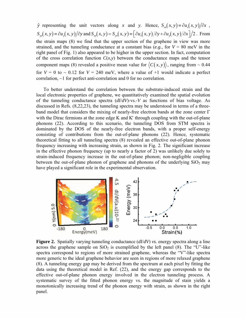
To better understand the correlation between the substrate-induced strain and the local electronic properties of graphene, we quantitatively examined the spatial evolution of the tunneling conductance spectra (dI/dV)-vs.-V as functions of bias voltage. As discussed in Refs. (8,22,23), the tunneling spectra may be understood in terms of a three-band model that considers the mixing of nearly-free electron bands at the zone center with the Dirac fermions at the zone edge K and K through coupling with the out-of-plane phonons (22). According to this scenario, the tunneling DOS from STM spectra is dominated by the DOS of the nearly-free electron bands, with a proper self-energy consisting of contributions from the out-of-plane phonons (22). Hence, systematic theoretical fitting to all tunneling spectra (8) revealed an effective out-of-plane phonon frequency increasing with increasing strain, as shown in Fig. 2. The significant increase in the effective phonon frequency (up to nearly a factor of 2) was unlikely due solely to strain-induced frequency increase in the out-of-plane phonon; non-negligible coupling between the out-of-plane phonon of graphene and phonons of the underlying SiO2 may have played a significant role in the experimental observation.
Figure 2. Spatially varying tunneling conductance (dI/dV) vs. energy spectra along a line across the graphene sample on SiO2 is exemplified by the left panel (8). The “U”-like spectra correspond to regions of more strained graphene, whereas the “V”-like spectra more generic to the ideal graphene behavior are seen in regions of more relaxed graphene (8). A tunneling energy gap may be derived from the spectrum at each pixel by fitting the data using the theoretical model in Ref. (22), and the energy gap corresponds to the effective out-of-plane phonon energy involved in the electron tunneling process. A systematic survey of the fitted phonon energy vs. the magnitude of stain yields a monotonically increasing trend of the phonon energy with strain, as shown in the right panel.

Despite apparent effects of substrate-induced strain on the electronic properties of mechanically exfoliated graphene, we note that such effects are mostly limited to low energies. As manifested by the tunneling conductance histograms of the graphene sample in Fig. 3, the spatial variations in the conductance become smaller with increasing bias voltage, suggesting increasing spatial homogeneity in the electronic DOS. Figure 3. Histograms of the tunneling conductance ratio in mechanically exfoliated graphene on SiO2, showing steadily decreasing variations (i.e. narrower linewidth in the histogram) with increasing bias voltage, from (a) V = 0, (b) V = 80 meV to (c) V = 240 meV, while the mean value of the tunneling conductance increases with increasing voltage, as expected for the DOS of Dirac fermions in graphene. CVD-Grown Graphene on Copper Foils
Systematic studies of the CVD grown graphene on Cu revealed a number of significant differences from the observation of mechanically exfoliated graphene on SiO2. First, much larger height variations in the former relative to those in the latter were found, as exemplified by the topographic images Figs. 4a – 4d and the corresponding height histograms in Figs. 4e – 4h. The ripple-like height variations over a relatively large scale in the CVD-grown graphene on Cu are consistent with previous reports (21) and are resultant from the large difference in the thermal expansion coefficients of graphene and Cu. That is, upon cooling the sample from ~ 1000°C to room temperature after the CVD growth of graphene, the less thermally contracted graphene can no longer remain flat on the Cu foil.
Second, the high-temperature CVD growth of graphene on Cu apparently incurred
significant lattice distortion to the arrangements of carbon atoms. As exemplified in the atomically resolved topographic image in Fig. 5a, different atomic arrangements were apparent in different regions of the (3.0 × 3.0) nm2 area in view. Specifically, we found that in a more relaxed region of the graphene sample (denoted as the -region) the atomic structure appeared to resemble the honeycomb or hexagon-like lattice with slight distortion. On the other hand, for spectra taken on the ridge (-region) of a ripple-like feature, the atomic arrangements deviated strongly from those of graphene, showing either nearly square-lattice or disordered atomic structure in the -region. Additionally, we note that there were completely disordered areas without atomic resolution (not shown in Fig. 5a) in the overall topographical survey, which we denote as the -region.
V = 0 V = 80 meV V = 240 meV
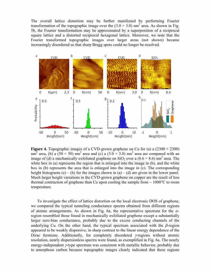
The overall lattice distortion may be further manifested by performing Fourier transformation of the topographic image over the (3.0 × 3.0) nm2 area. As shown in Fig. 5b, the Fourier transformation may be approximated by a superposition of a reciprocal square lattice and a distorted reciprocal hexagonal lattice. Moreover, we note that the Fourier transformed topographic images over larger areas (not shown) became increasingly disordered so that sharp Bragg spots could no longer be resolved. Figure 4. Topographic images of a CVD-grown graphene on Cu for (a) a (2300 × 2300) nm2 area, (b) a (50 × 50) nm2 area and (c) a (3.0 × 3.0) nm2 area are compared with an image of (d) a mechanically exfoliated graphene on SiO2 over a (8.6 × 8.6) nm2 area. The white box in (a) represents the region that is enlarged into the image in (b), and the white box in (b) represents the area that is enlarged into the image in (c). The corresponding height histograms (e) – (h) for the images shown in (a) – (d) are given in the lower panel. Much larger height variations in the CVD-grown graphene on copper are the result of less thermal contraction of graphene than Cu upon cooling the sample from ~ 1000°C to room temperature.
To investigate the effect of lattice distortion on the local electronic DOS of graphene, we compared the typical tunneling conductance spectra obtained from different regions of atomic arrangements. As shown in Fig. 6a, the representative spectrum for the -region resembled those found in mechanically exfoliated graphene except a substantially larger zero-bias conductance, probably due to the excess conducting channels of the underlying Cu. On the other hand, the typical spectrum associated with the -region appeared to be weakly dispersive, in sharp contrast to the linear energy dependence of the Dirac fermions. Additionally, for completely disordered -regions without atomic resolution, nearly dispersionless spectra were found, as exemplified in Fig. 6a. The nearly energy-independent -type spectrum was consistent with metallic behavior, probably due to amorphous carbon because topographic images clearly indicated that these regions

were covered by carbon rather than the bare Cu foil. Therefore, the strong deviation of the tunneling spectrum in the and -regions was apparently related to the different carbon atomic arrangements induced by the CVD-growth on Cu. Figure 5. Lattice distortion of the CVD-grown graphene on Cu: (a) A representative atomically resolved topography over a (3.0 × 3.0) nm2 area, showing different atomic arrangements of the graphene sample in view, with slightly skewed honeycomb (or hexagonal) lattices in the -region and a combination of nearly squared and disordered atomic arrangements in the -region. (b) Fourier transformation of the topographic image in (a), showing the superposition of an approximately square reciprocal lattice and a strongly distorted hexagonal reciprocal lattice. The above comparison of STM/STS studies of mechanically exfoliated graphene on SiO2 and CVD-grown graphene on Cu clearly underscores the importance of carbon atomic structures to the resultant electronic DOS of graphene and the strong influence of both dielectrics and metals that are proximate to the mono-layer graphene. These findings are highly relevant to the development of graphene-based electronics, because all electronic device structures require depositing electrodes and gated dielectric materials to graphene. One possible means to mitigating the degradation of graphene properties is to consider the use of bi-layer or multi-layer graphene, with the outer layers designated to facilitating electrical contacts and gated dielectric materials while the intact inner layer of graphene retains its superior properties. Furthermore, one may consider taking advantage of the active nature of -electrons to devise means of modifying the electronic properties of graphene in a controlled manner for desirable functionality.
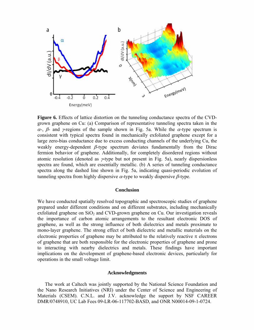
Figure 6. Effects of lattice distortion on the tunneling conductance spectra of the CVD-grown graphene on Cu: (a) Comparison of representative tunneling spectra taken in the -, - and -regions of the sample shown in Fig. 5a. While the -type spectrum is consistent with typical spectra found in mechanically exfoliated graphene except for a large zero-bias conductance due to excess conducting channels of the underlying Cu, the weakly energy-dependent -type spectrum deviates fundamentally from the Dirac fermion behavior of graphene. Additionally, for completely disordered regions without atomic resolution (denoted as -type but not present in Fig. 5a), nearly dispersionless spectra are found, which are essentially metallic. (b) A series of tunneling conductance spectra along the dashed line shown in Fig. 5a, indicating quasi-periodic evolution of tunneling spectra from highly dispersive -type to weakly dispersive -type.
Conclusion
We have conducted spatially resolved topographic and spectroscopic studies of graphene prepared under different conditions and on different substrates, including mechanically exfoliated graphene on SiO2 and CVD-grown graphene on Cu. Our investigation reveals the importance of carbon atomic arrangements to the resultant electronic DOS of graphene, as well as the strong influence of both dielectrics and metals proximate to mono-layer graphene. The strong effect of both dielectric and metallic materials on the electronic properties of graphene may be attributed to the relatively reactive electrons of graphene that are both responsible for the electronic properties of graphene and prone to interacting with nearby dielectrics and metals. These findings have important implications on the development of graphene-based electronic devices, particularly for operations in the small voltage limit.
Acknowledgments
The work at Caltech was jointly supported by the National Science Foundation and
the Nano Research Initiatives (NRI) under the Center of Science and Engineering of Materials (CSEM). C.N.L. and J.V. acknowledge the support by NSF CAREER DMR/0748910, UC Lab Fees 09-LR-06-117702-BASD, and ONR N00014-09-1-0724.
a b

References
1. K. S. Novoselov et al., Nature, 438, 197 (2005). 2. A. K. Geim and K. S. Novoselov, Nat. Mater., 6, 183 (2007). 3. F. Miao et al., Science, 317, 1530 (2007). 4. Y. B. Zhang, Y. W. Tan, H. L. Stormer, and P. Kim, Nature, 438, 201 (2005). 5. B. Standley et al., Nano Lett., 8, 3345 (2008). 6. N. Tombros et al., Nature, 448, 571 (2007). 7. X. Wang, L. J. Zhi, and K. Mullen, Nano Lett., 8, 323 (2008). 8. M. L. Teague et al., Nano Lett., 9, 2542 (2009). 9. P. Malle et al., Phys. Rev. B, 76, 041403 (2007). 10. C. Berger et al., Science, 312, 1991 (2006). 11. K. V. Emtsev et al., Nat. Mater., 8, 203 (2009). 12. S. Stankovich et al., Carbon, 45, 1558 (2008). 13. G. Eda et al., Nat. Nanotechnol., 3, 270 (2008). 14. P. W. Sutter, J.-I. Flege, E. A. Sutter, Nat. Mater., 7, 406 (2008). 15. A. L. V. de Parga et al., Phys. Rev. Lett., 100, 056807 (2008). 16. A. Reina et al., Nano Lett., 9, 30 (2009). 17. K. S. Kim et al., Nature, 457, 706 (2009). 18. H. Ueta et al., Surf. Sci., 560, 183 (2004). 19. D. E. Starr et al., Surf. Sci., 600, 2688 (2006). 20. J. Vaari et al., Catal. Lett., 44, 43 (1997). 21. X. Li et al., Science, 324, 1312 (2009). 22. T. O. Wehling, I. Grigorenko, A. I. Lichtenstein, and A. V. Balatsky, Phys. Rev.
Lett., 101, 216803 (2008). 23. Y. B. Zhang et al., Nat. Phys. 4, 627 (2008).
Copyright © 2022 FDOKUMEN