Infrared absorption in thin metallic films
203
lot-''t t.: UNIVERSITY OF ADELAIDE PHYSICS DEPARTMENT THESIS FOR THE DEGREE OF MASTER OF SCIENCE INFRARED ABSORPTION IN THIN METALLIC FILIUS K.C. Liddiard, B.Sc. (Hons) Researcl'r Scientist Australian Defence Scientific Service WEAPONS RESEARCH ESTABLISHMENT, SALISBURY, SOUTH AUSTRALIA I il I -t .ì .t il .l : '.1 I I L973
-
Upload
khangminh22 -
Category
Documents
-
view
3 -
download
0
Transcript of Infrared absorption in thin metallic films

lot-''t
t.:
UNIVERSITY OF ADELAIDE
PHYSICS DEPARTMENT
THESIS FOR THE DEGREE OF MASTER OF SCIENCE
INFRARED ABSORPTION IN THIN METALLIC FILIUS
K.C. Liddiard, B.Sc. (Hons)Researcl'r ScientistAustralian Defence Scientific Service
WEAPONS RESEARCH ESTABLISHMENT,SALISBURY, SOUTH AUSTRALIA
I
il
I
-t
.ì.t
il.l
:
'.1
II
L973
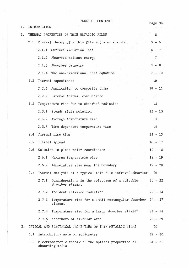
TABLE OF CONTENTS
1. INTRODUCTION
2. T}IERMAL PROPERTIES OF THIN METALLIC FILMS
2.L Tt¡ernal theory of a thin fihn infrared absorber
2.L.7 Surface radiation loss
2.L,2 Absorbed radiant energy
2.I.3 Absorber geometry
2.t,4 The one-dimensional heat equation
2.2 Thermal capacitance
2.2.L Application to composite filns
2.2.2 Lateral thermal conductance
2.3 Temperature rise due to absorbecl radiation
2.3.I Steady state solution
2.3.2 Average tenperature rise
2.3.3 Time dependent tenperature rise
2,4 Thermal rise time
2,5 Thermal spread
2.6 Solution in plane polar coordinates
2,6.L Maximum temperature rise
2.6.2 Temperature rise near the boundary
2.7 Therrnal analysis of a typical thin film infrared absorber
2.7.L Considerations in the selection of a suitableabsorber element
2.7.2 Incident infrared radiation
2.7,3 Temperature rise for a sna11 rectangular absorberelement
2.7.4 Temperature rise for a large absorber elenent
2.7.! Absorbers of circular area
3, OPTICAT A}ID ELECTRICAL PROPERTIES OF TIIIN METALLIC FILMS
3.1 Introductory note on radionetry
3.2 Electromagnetic theory of the optical properties ofabsorbing media
PageL
5
5-
6-
7
7-
8-
L0
10-
1L
72
1,2 -
73
74
14-
16-
17-
18-
19-
20
20-
No.
6
7
B
10
11
T3
1s
17
18
19
20
22
22-24
24-27
27-28
28-29
29
29-30
37-32

4
3.2.L Absorption in netals
3.3 Thermal radiation sources
3.4 Infrared absorytion in thin metallic films
3.4.I Dependence of absorption on angle of incidence
3.4.2 Influence of the plastic substrate film
3.4.3 Double netal film
3.5 Electrical conduction in thin netallic films
3.5.1 Theory of conduction in continuous netal filns
NUCLEATION AND GROWTH PROCESSES AND THE STRUCTURE OF THINMETALLIC FILNIS
4.t Introductory concepts
4.t.1 Adsorption of vapour atons
4.1.2 Initial nucleation
4,2 Observed nucleation and growth phenonena
4.2.1 Adatorn surface mobility and film aggloneration
4.2.2 The growth sequence
4.2,3 Filn structure
4.2,4 Substrate transítion temperatures
4.3 Electrical çonduction
4.3.L Final filn resistance
4.3.2 Aging effects
4.3.3 Electrostatic charge effects
4.4 Selection of suitable netals for thin filn infraredabsorbers
4 .4 .7 Gol d fi lms
4.4.2 Platinun filns
4,4.3 Nickel filns
4.4,4 Alloy filns
PREPARATION OF METALLIC FILMS
5.1 Vacuun coating unit
Page No.
32-34
34
35-36
37
37-39
59
39-40
40-43
4s
43
43-45
45-48
48
48-49
49-50
50-sl
51 - s3
53
53-54
54-56
s6-57
57 - 59
59
59-60
60
60-61
61
6r-62
5

5,2
5.3
5.4
5.5
5.6
5.7
5.8
5.9
5.1.1 Anci1lary coating unit
Deposition control techniques
5.2,7 Film resistance
5.2,2 Deposition rate and film thickness
5.2.3 Chamber pressure
5,2.4 Deposition time
Substrates
5. 5. 1 Resis tance measurement
5.3.2 Thickness monitor sensing head
5. 3. 3 Thickness measurenent
5.3.4 Infrared measurements
5.3.5 Electron nicroscopy
5.3.6 Measurement of thernal properties
5.3.7 Measurenent of film resistance on plastíc substrates
Preparation of polyner filn substrates
5.4.1 Ce11u1ose nitrate
5.4.2 Polyvinyl formal
5.4,3 Polyúinyl chloride
5.4,4 Chlorinated PVC
5.4.5 Polyvinylidene chloride - acrylonitrite copolymer
5,4.6 Preparation of sel.f-supporting filns
5.4.7 Selected polymer films
Cleaning and handling of substrates
Deposition of gold films
Deposition of chroniun filns
Deposition of nichrome films
Deposi-tion of nickel fílns
5.9.1 Filanent vapour source deposition
Page No.
62
62-63
63-64
64-65
65-66
66
66-67
67-68
68
68
68-69
69
69
70
70-71
7T
77
77-72
72
72
72-73
73-7s
75-76
76
76-77
77
77
78
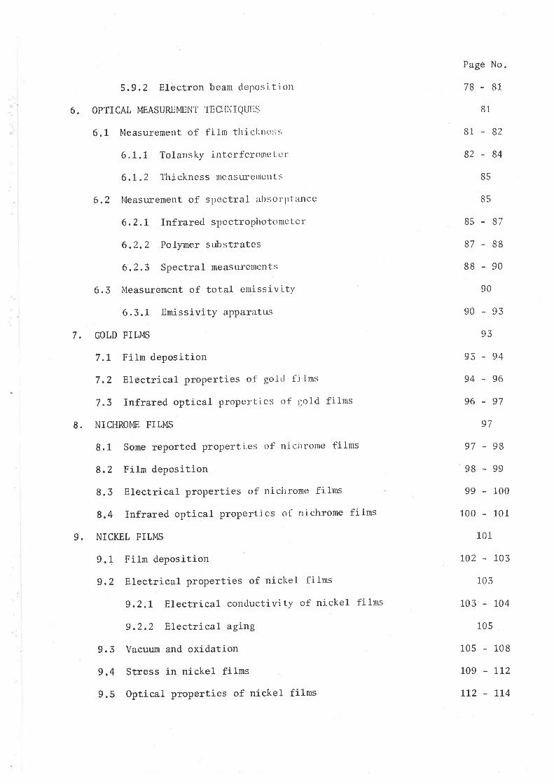
5.9 ,2 Electron bearn dePosi tiorr
6. OPTICAL MEASUREMENT TECIINIQUTJS
6 . 1 Measurement of f i lm thi clllìcri; s
6.1.1 TolanskY illterfcrolnct cl:
6.L.2 Thickness llìeasureìllclìts
6.2 lr{easurement of s¡rectral ab-sor:¡rf attce
6,2.I Infrared spectropitotomctcr
6.2.2 Polyner substrates
6.2.3 Spectral measurenlent:i
6.3 Measurement of total enrissivLty
6.3,I Emissivity apparatus
7. GOLD FILMS
7.L Filn deposition
7.2 Electrical properties ol" golcl films
7.3 Infrared optical propertics of ¡¡oJ'd films
8. NICHROME FILMS
8.1 Sone reported properties of nicltrome films
8.2 Film deposition
8.3 Electrical properties of nic.ltrome films
8.4 Infrared optical properties of nichrome films
9. NICKEL FILMS
9.1 Film deposition
9.2 Electrical properties of ni-ckel films
9.2.I Electrical conductivity of nickel filns
9.2,2 Electrical aging
9.3 Vacuum and oxidation
9.4 Stress in nickel filns
9.5 Optical properties of nickel films
Page No.
78-81
8L
81, - 82
82-84
B5
85
85-87
87-88
88-90
90
90-93
93
93-94
94-96
96-97
97
97-98
98-99
99 - 100
100 - 101
101
702 - I03
103
105 - 104
10s
105 - 108
r09 - Ltz
LT2 - 7L4

L2.
L3,
11.5.5 Nickel fifuns
11.6 Measurement of tenperature rise
lI.7 Summary of thernal properties
CONCLUSIONS
ACKNOWLEDGEMENTS
LIST OF REFERENCES
SYMBOL TABLE
LIST OF TABLES
1. BULK THERIvIAL PROPERTIES OF SELECTED ABSORBER MATERIATS
2. COMPUTED THERMAL PARAMETERS
3. SELECTED POLYMER FILMS
4. SPECIMENS FOR TI]ERMAL MEASUREMENTS
5. SI,JM},IARY OF THERMAL RISE TIME IvIEASUREMENTS
6. SI.JMMARY OF THERMAL SPREAD MEASUREMENTS
7. TEMPERATURE RISE IUEASURENÍENTS
Page I'lo.
L4L - T44
L44 - 746
L46 - t48
148
150
22
26
74
t28
135
t4I
t46
LIST OF F'IGUIìES
1. Steady state ternperature ri-se. Selected metallic absorbers
2. Tine dependent temperature rise. lrlickel absorber
3. Time dependent average temperature rise. Selected metallic absorbers
4. Time dependent temperature rise. Large area nickel absorber
5. Steady state temperaturc rise for rectangular and circular absorber elements
6. Blackbody radiation for three selected tenperatures
7, Infrared optical propcrties of a thir"r metallic film
8. Dependence of infrarecl optical propertics on angle of incidence
9. Conductivity of thin filns accordi-ng to Fuchs-Sondhierner theory
10. Vacuum coatjng unit
11. Depositj-on control instrumentation
12. Monitor ci-rcuit schematic
13. Stibstrate arra:rgement
14. Apparatus for the preparation of polyrner films
15. Electron beam deposition source
16. Tolansky nultiple beam interferometer
17. Tolarisky fringe pattern
18. Infrared spectrophotometer
19. Spectral absorption of collodion substrates
20, Enis-sivity test apparatus
2t, Chart recording of elnissivity measutentent
22. Quartz crystal monitor calibration f.or .qolcl films
23. Emissivity of gold films
24. Quartz crystal monitor calibration for nichrone films
25. Resistance of nichrome films
26. Quartz crystal nonitor calibration for nicl<el films
27. Resistance of nickel films on glass substratc-s
28. Resistance of nickel filns on collodion stilrstrates
29. Enissivity of nickel fil¡ns
30. Absorptance and transmittance of nickel fil¡ns
51. Structr¡re of formvar substrates
32. Structure of collodion substrates
33. Influence of coll.odion substrates in electron nicroscopy
54. Structr¡re of gold filrns 1
55. Structt¡re of gold films 2
36. Structure of nichrone filns
37. Structure of nickel films
38. Stress in nickel filn on for¡nvar strbstrate
39. Thermal rise tine neasurement. Oscilloscope display
40. Thermal rise tine for a gold absorber filn
41. Thernal rise tine for a nickel absorber filn
42. Steady state temperature rise. Gold absorber film
43, Steady state tenperature rise. Nickel absorber filn
SUMMARY
This thesis describes research studies on the absorption of infrared
radiation in thin metallic films. Thin films of nickel, gold and a nickel-
chromium alloy welre vacuum deposited on to freely-supported polymer menbrane
substrates. It is intended that these films will comprise the radiation receiver
element of ltigh performance infrared detectors.
The research is broadly divided into two nain areas of study. These
are the infrared optical properties of the selected metal filns, and thermal
properties relevant to the absorption process suçh as ternperature rise, thermal
rise tine and thernal spread in the plane of the fi1m. Tlre therrnal characteris-
tics are of fundamental inportance in infr¿rred detector research, because they
determine sensitivity, speed of response and optical inage quality.
The first part of the thesis is concerned with a tl-reoretical analysis
of the thernal and infrared optical properties of metallic absorber filns, and
includes a resume of nucleation and growth phenomenon in vacuum deposited metal
fi1ns. This is followed by a description of measurenent techniques and the
apparatus used for the preparation of netal fi1ms, curd thcn a cletailed discussion
of experinental results. Careful consideration was given to the influence of
deposition paraneters, and a study was made of the structure of the filns using
conventional bright field electron nicroscopy. Finally, the experimental results
are conpared with theoretical predictions.
In general, good agreernent was found between the theoretical analysis
and the measured optical and thermal properties of the selected metal absorber
filns. This encouraging result enables us to predict the nost suitable metal,
and the optirnurn deposition paraneters, to satisfy specific requirements in infrared
detector research.
STATEMENT
I herewith state that this thesis does not contain any naterial
whictr has been accepted for the award of any other degree or diplona in
any University and that, to the best of ny knowledge and belief, the thesis
contains no naterial previously published or hlritten by any other person,
except when due referenco is nade in the text of the thesis.
1-. INTRODUCTIOT]
This thesis describes research into the physics of the absorption of infra-
red radiation in thin metallic films vacuum deposited on to plastic mernbrare
substrates. The aim of the project rvas to deduce, fron fundamental considera-
tions, the desired properties and optirnum nethod of preparation of a simple
and efficient infrared absorbing filrn, which would form the radiation receiver
elernent of a thermal infrared detector.
It is emphasised that the thesis is not concerned explicitly with the study
of infrared detectors; nevertheless r{e should bear in nrind the project
motivation expressed above, as this must inevitably influence the direction
along which research should proceed. It is tlrerefore desiral-rle that lve
briefly consider the various factors which influence the perfortilance of the
thermal detector.
Therrnal infrared detectors are distinguished by the common characteristic
that the heating effect of the incident infrared radiation causes a measurable
change in some physical property of the detector. The temperature sensitive
property may be any one of an extensive list of physical parameters, ê.9.,
electrical resistance or capacitance, mechanical flexure, thermoelectric power,
e¡pansion of a gas, vapour pressure, optical reflectance, etc. The detector
itself is comprised of three basic components, narnely an infrared absorber,
a temperature sensitive element and a suitable substrate or mechanical support.
Depending on the detector type, the individual components need not be discrete;
thus the temperature sensitive element may also function as a substrate for
the absorber.
In this thesis we consider an irnportant group of detectors in whicl'r tl.re
infrared absorber is deposited on to a thin self-supporting pellicle. Tiris
group includes the thin filn resistance boloneter, the dielectric boloneter and
various types of infrared imaging sensors. l\re will be concerned only with the
infrared absorber conponent of the detector. No mention will be made
'r11
k"\*Vi'-;t,%r;:-
)
explicitly of the ternperature sensitive component, nor of rnethods of signal
processing. It is important to note, however, that the optical and thermal
theory presented in the thesis can be extended to include the temperature
sensitive element, ild hence nay be used to predict the performance of tiris
particular group of detectors.
The first requirenent of an efficient thernal cletector is that the change
r^ritlÌ tenperature of the relevant temperature sensitive physical property (its
tternperature coefficientr) should be of sufficient magnitude to permit the
detection of the desired signal leve1. Trvo additional factors influence the
performance of the thermal detector :
(a) the tenperature rise following radiation exposure must be as high
as possible, and
(b) the thernal rise tirne must be sufficiently fast to achi-eve the
desired information rate.
These factors are strongly related to the physical characteristics of the
infrared absorber element, and must therefore be considered in this project.
As we would expect, the most suitable metallic film must have an absorytance
approaching theoretical maximum. It should also be electrical ly stable a¡rd
thermally uniform. Furthermore, if the film is to be supported in vacuo, Ðd
suffers surface heat loss solely by radiation exchange witlr its nearby back-
ground, then in order that it may respond rapidly to changes in incident radiant
energy, it must possess rninimum thermal capacitance. It will be shown that this
last requirempnt is met by the thinnest possible filn satisfying the desired
optical properties.
In addition to radiation exchange, the absorber filn wíl1 also suffer heat
loss through thermal conduction to the support on which the filn is nounted.
This thermal spread in the plane of the film wiLl cause a reduction in the speed
of response, but also a decrease in the average temperature rise of the absorber
-3-
elenent. The magnitude of the effect depends on the therntal conductivity of
the absorber and again on film thickness. Thermal spread will becone
increasingly significant as the size of the absorber elelnent becomes snal1er.
In practice, the absorber element of an infrared detector tvould normally have
a surface area of Lmn2 or less; therefore tlie modifications to the thermal
properties of an absorber filn due to a reduction in surface dimensions should
also be considered in this study.
We should note here that the need to keep both thernal capacitance and
lateral heat spread to a minimum is the main reason for the selection of thin
metallic films for many detector applications, i-n preference to other well
known types of infrared absorbers.
The use of thin plastic substrates is particularly appropriate for experi-
mental investigations because of ease of preparation and high infrared trans-
mission. Flowever, these films do contribute subsEartially to the overall
thermal capacitance; hence in the ideal situation the ntetallic absorber films
should be self-supporting. Unfortunately, with the exception of the metal film
resistance boloneter detector (which is self-absorbing), this ideal has no
practical va1ue, because a temperature sensitive material will always be
required. Nevertheless, experience has shorvn that we should seek one further
property, namely that the netallic film should be structurally continuous.
The research described in the tl'resis is broadly divided into two main areas
of study. These are the optical properties of metallic absorber films in the
8 to 14 Un wavelength region of the electromagnetic spectrum, specifically the
Tesponse to blackbody radiation near ambient temperature; and thernal proper-
ties relevant to the absorption process such as temperature rise due to the
absorbed radiation, therrnal rise time and lateral heat spread. Thermal
properties are discussed in the opening sections. A tl-reory is established
which gives the relationship between various thermal paraneters, subsequently
4
leading to the selection of a suitable type of metal for experimental studies.
This is followed by a sumnary of the electromagnetic theory of infrared
absorption in netallic filns, underlining the fundanental relationship between
optical absorption and electrical conductivity.
In view of tire inportance of electrical conductivity, wirich is structure
dependent, ffid the desire to achieve structural continuity, sonte thought should
also be accorded to the nechanisrn of filn formation. A brief resume is there-
fore given of the nucleation and growth process in vacuum deposited metallic
filns. From our current understanding of the physics of this phenomenon we are
able to place further empl'rasis on the particular choice of metals selected for
study.
Based on the theoretical consíderations nentioned above, nickel was event-
ually chosen for detailed experinental investigation. Some results are also
included, for comparison puryoses, of a brief study of gold and a nickel-
chrornium alloy.
The final sections of the thesis are devoted to a description of the
apparatus r¡sed to prepare the netallic filns and a detailed account of the
experimental results. The experinental investigation is rnainly concerned
with the dependence of the optical and thermal properties of nickel filns on
conditions of evaporation, thickness, electrical conductivity and film
structure. The results are compared with theoretical predictions.
Syrnbols used for physical quarìtities are in accordatce with British
Standards, except in radiometry where symbols are basecl on widely accepted
notation. This has caused duplication in some instances. Horrrever, care has
been taken to avoid duplication in the sane Sections of the thesis. SI units
are used throughout, except for length which is expressed in cm. This is in
accord with corunon practice in infrared technology. As a consequence, density
is given in g..r-5. Other subnultiples, permissible trnder the Standard, are

-5-
used
2.1
where convenient for the expression of physical data.
2. T}IERMAL PROPERTIES OF THIN MLTALLIC FILMS
Thermal theory of a thin film infrared absorber
The tenperature distribution in the plane of a thin solid filn
in vacuo depends upon thermal balance between conduction loss to the
nounts on which the film is supported, surface radiation exchange with
the nearby surroundings and the rate of generation of heat within the
film. Since the netallic films considered in this thesis are extrernely
thin, Í¡e can assune that the temperature is independent of thickness
and the problen then reduces to that of a solution to the two-dimensional
equation of heat conduction in a thin netallic plate with radiation loss
at its surface. For the present hre nay ignore the plastic nembrane
substrate; its influence can be introduced without loss of generality
at a later stage.
If the filn has a rectangular area, lying on the x-y plane, then the
temperature at any point can, in principle, be determined fron the
solution to the eouation :
o" ïî = -[#.:jt] F(r) + B(x,v,t) (1)
hrhere T = absolute temperature (oK) at x,y,t
t = time (second)
K = thermal conductivity (w.cnll oK-l)
p = density (g."^-5)
c = specific heat (.1.g-.1 oK-l)
F(T)= surface flux loss per unit volume due to radiation
exchange (w. cm-S)
B(x,)r,t)= rate of generation of heat within the film lW.cm-3)
For a filn of circular surface area, the heat equation can be
expressed in plane polar co-ordinates on carrying out the usual trans-
-6-
formations.
As it stands, ful1 solutions to equation (1) are not easily obtained.
In particular, there is no exact solution to this problem for surface
radiation loss according to the Stefan-Boltzmann fourth power 1aw.
In practice, however, we find that suitable approxintations can be made
which yield solutions of sufficient accuracy for many applications.
The most important simplification is the assumption of a linear radiation
1aw, as explained below.
2.1.t Surface radiation loss
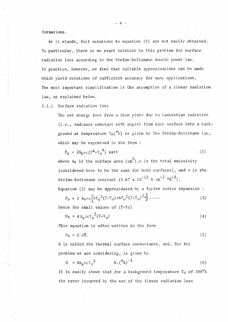
TIte net energy loss from a thin plate due to Lambertian radiation
(i.e., radiance constant with angle) from each surface into a back-
ground at temperature fo(oK) is given by the Stefan-Boltzrnann 1atv,
rvhich may be expressed in the form :
P, = 2\or(t4-To4) watt (2)
where A5 is the surface area (.t2),e is tlre total emissivity
(considered here to be the sane for both surfaces) , üd o is the
Stefan-Boltzmann constant (5.67 x 10⁻¹² u . -2 oK-l).
Equation (2) nay be approxinated by a Taylor series expansion :
ps -- 2 nso.[+ro3(r-ro) *6ro2(r-10) 'z| . -,.. (i)
Hence for small values of (T-To)
Ps = SAroeToS(T-To) (4)
This equation is often written in the form
Ps=GAT. (5)
G is calted the thernal surface conductance, and, for the
problen we are considering, is given by
G = 8AroeToS w.(ox)-l (6)
It is easily shown that for a background tempeïature Te of 300oK
the error incurred by the use of the linear radiation loss
2.L.2
2.I.3
-7-
approxination is 2.5% when the temperature difference (T-To) is
5 deg K rising to 28vo for a temperature difference of 50 deg K.
In this investigation we will not consider values of (T-T6) greater
than several degrees.
Absorbed radiant energy
The second sirnplification we carr make to the heat conduction
equation is in our selection of tl're forn for the expression
B(x,y,t). This quantity is just the absorbed energy due to radiant
power incident on the rnetallic filn fron some remote infrared source.
We shall assume that this radia¡rt poì4'er is absorbed uniformly
throughout the fi1n, and that the radiation exposure is long
compared to the thermal tine constant of the film.
The assumption of a constant value for B(x,y,t) in no way
detracts fron the study of the thermal properties of the netallic
filns. It is of interest to note that in the practical application
of infrared detectors any forn of modulation of the incident radiant
is usually chosen to have a period which is greater than the
detector response tine. In the present study, the only
advantage to be gained by the use of nodulated radiation is in the
estimation of thermal rise tine; but this can just as easily be
determined from a step function forn of incident irradiation.
Absorber geometry
The final simplification lies in the choice of the surface
geo¡netly of the metallic filrn. There are two geonetries of
particular interest in this investigation:
(a) In nost of the experinental study films are supported on
circular mounting rings. In this case, the thernal contours
in the filn should be radially syrnnetric. If the diarneter
2.r.4
-8-
of the film is sufficiently large, then lateral conduction
loss to the mounting rings is predonina¡rt only over a region
near the filn boundary whiclì may be approximated by one-
dimensional heat florv, and the temperature at the centre of
the film then depends only on radiation excharge rvith the
background.
(b) An inportant concept associated rvith the practical applica-
tions of infrared radiation detectors is that the absorber
elenent should be as sma1l as possible. It is therefore of
considerable interest to exanine the mechanism of lateral
spread of heat in thin metallic films of smal1 surface area.
In this study it will be sufficient to consider the flol of
heat in a rectangular film supported at two opposing edges
by a solid heat sink at tenperature Te(of). If we assume that
the film is both homogeueous ald isotropic we can then quite
reasonably reduce the problem to one of linear heat flow along
the length of the film between the supports.
The one-dinensional heat equation
The simplifications we nay now apply to the general heat
equation (1) arising fron the discussions of the preceding sub-
sections enable us to deduce nearly al1 of the thermal properties
relevant to this study. ltle shall find that many of the results
are applicable to various film geometries. The validity of the
results will be demonstrated in a later section by solving the
equivalent equation in plane polar coordinates.
Let us assume that a rectangular metallic filln of lengtl-r.C and
width w, with its lengtl'r para1le1 to the x-axis, is freely
supported in vacuo at x = 0, !" by a solid heat sink at temperature
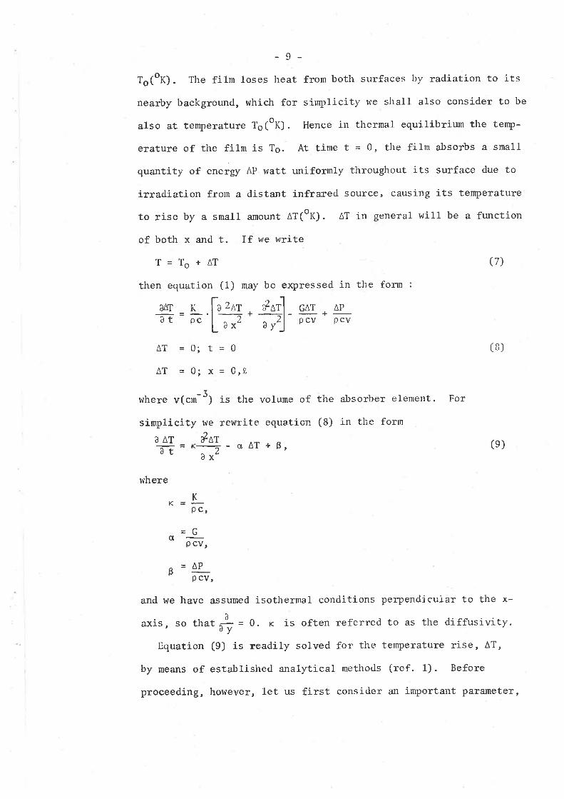
-9-
To(oK). The filn loses heat fron both surfaces by radiation to its
nearby background, which for sirnplicity we sl'rall also consider to be
also at temperature Te(ot<). Hence in thermal equilibrium the temp-
erature of the filn is To' At time t = 0, the filrn absqrbs a snall
quantity of energy AP watt uniformly throughout its surface due to
irradiation frorn a distant infrared source' causing its temperature
to rise by a small anount AT(oK). AT in general will be a fimction
of both x and t. If we write
T=To+AT (7)
then equation (1) nay be expressed in tlre forrn :
r--'1â^r K I a 2¡r #¡rl c¡r AP
-=-.1-¡-¡!-
At pc I " 2 ^ 2l pcv pcvLöx 'òyJ
AT -0;t=0 (B)
AT = 0; x = 0r0
where v(c*-5) is the volume of the absorber elernent. For
simplicity we rewrite equation (8) in tlie form
â AT &nr-;= = r:-:å _ a AT + ß,oL ^ ¿dx(e)
where
KK =- 9C¡
Ê
=G0 CV¡
=API CVr
and we have assuned isotherrnal conditions perpendi.cuiar to the x-d
axis. so that,å = 0. r is often referred to as the diffusivity.' dy
Iìquation (9) is readily solved for thc: temperature rise, AT,
by neans of established analytical metirods (ref. 1). Before
proceeding, however, let us first consider an importallt par¿Lmeter,
0a
-10-
the thermal capacitance of the film, rvhich appears inplicitly
in the above equations.
2.2 Thermal capacitance
The thernal capacitance of the thin absorbing film is, by definition,
Ç = pCV
= pcA5t (,¡or-1) (10)
rvhence
K= KA5t--
O= G
e
ßAP
T_ (1 1)
where t is the film thickness. In keeping with convention t is uSed
for both tine and thickness. Since time appears only in the differential
equations and their innediate solutions and thi-ckness does not appear
explicitly in the sane equations, no confusion should arise fron this
dupli cation.
The inporta¡rce of the thernal capacitance is, as we sha1l see, tl'rat
it deternines the extent to which the filn stores heat, and hence its
ability to respond to fluctuations in incident radiation. The concept
of a sinple thermal capacitance nay also, in certain circumstances, be
extended to a nultilayer filn.
2.2.7 Application to conposite films
Let us now consider a conposite film consisting of several
layers of different materials, each layer having its own character-
istic value of p and c. Then providing the temperature at any time
and at any given coordinate (x,y) in the plane of the filn is
assu¡ned to be independent of thickness, i.€., is the sane at all
points through the filn, the total thermal capacitance is :
C = As (prcrtr + prcz tz + p3cst3 +....) (I2)

2.2.2
-11 -
The concept of a I lumpedr thermal capacitance sinply means that
a rise in tenperatule is transmitted from the upper to the lower
surfaces of the conposite film in a tine very much less than the
thernal rise tine of the entire film. It car be readily shown that
this is indeed the case for very thin filns of thickness small
compared to the surface dimensions.
Carslarv and Jaeger (reference 1' Page 100) llave considered the
case of heat transfer across a slab, one face of which is held at
a constant temperature and the other face thermally insulated' This
exanple approximates a thin metallic absorber film deposited onto
a plastic membrane in vacuo, for here we may assume that the
mernbrane represents the slab, one surface of which is insta¡rtaneously
raised to the absorber tenperature. A sirnple calculation shows that
for a filn thickness of 1000R the opposite face of the rnembra¡e
rises tO absorber temperature in a time less than 1 Us, which is
negligible compared to the typical thernal time constant.
Lateral thermal conductance
The assumption of a lurnped thermal capacitance also enables us
to extend the diffusivity to include cornposite filns. The quafitity
I(t nay be referred to as tlte lateral thermal concluctance of a thin
film (ref. 2). Fron tire above discussion, it is evident that we
can substitute in equation (11)
I(t = Krt, * K2tZ * K3t3 + ..... (13)
where K1,K2rKg, are the thermal conductivities of the compon-
ent layers of the composite fi1n. Hence heat diffuses uniformly
along the filn as if it had a single diffusivity deternined by
equations (f f ) , G2) and (13) .
-L2-
2.3 Temperature rise due to absorbed radiation
Provided the assumption of a lunped thernal capacitance is va1id, the
solution to equation (9) for the temperature rise in the absorber film is
applicable to both the metallic film by itself and the absorber-¡nembrate
composite filn. Note, however, that if the enissivíty is not the same
for both sides of the conposite film, then equation (6) nust be nultiplied
Uy (et + e2)f2, wlr^ete e' eZ are the enissivities of the two surfaces.
Equation (9) is readily solved (see, e.g. ref. 1) by letting
AT = ATr + AT2 (14)
where AT1 is tine independent and satisfies2
d-ÂTrK---¡' -oAT1 +ß=0¿*2 (1s)
ATr = 0; x=Orl
arìd AT2 is a firnction of both x and t and satisfies
â ATr azlTz--ãË - * -æ- a ^t2
ATz - 0; x=0,1 (16)
LTZ = AT;t=0
The solution to the tine independent equation (15) represents the
important case of steady s Eate temperature and deserves detailed
examination.
2.3.I Steady state solution
lVhen the tine is large conpared to the thermal tine constant
of the filn, equation (15) yields the steady state solution :
Ir (17)I
It follows that the maxinun temperature rise for a film of
finite length ocçurs at the mid point, when

-13-
arr=*,t-ru"nf) (18)
The ratio ß/q has particular significance. If the film r4las not
terninated at x - f,, but was of infiníte length, then the solution
to the steady state conduction equation would be :
R-Ar = å (r -"-ux, (1s)
Thus, in this case, when x is large the temperature rise attains
the theoretical maximurn value
AT (20)o
AP=-G
It is evident from equation (18) that the tenperature at the
centre of a finite filn approaches the maxinum value when l, is
large. Also, if the absorbed energy AP is due to an incident
infrared irradiance of Ho (w.cn-2) then fron equation (6) it
follows that the maxinum temperature rise is independent of both
enissivity and area, and for a given value of To depends only on
the nagnitude of Ho.
Average temperature rise
When lateral conduction loss to the film supports is significant
it is often of value to estinate the average temperature rise under
steady state conditions. This is given by
qcx,
2.3.2
dxAT^ra=+
(2r)
Carrying out the integration we find that
AT = ÀT' |-, - z / cosrr u!'-r\'ìu,.=uro.Lr__\_ffi_il (22)
The average tenperature rise approaches the uraximum value when
l, is large or, for a given length, when 1/u is small.

t4
2,3.3 Time dependent tenperature rise
on solving equation (16) and adding equation (17) we arrive at
the full solution of the heat conduction equation :
AT = ATs , ATo,IT L r,2 .sin (2n-1)nx.
n=1(2n- 1) (2n- 1) +.Q,
9"
2
u (23)
t {.2
r,]]exp . ot-t (2n-1,)
This is a slowly conveïgent series and in order to obtain
sufficiently accutate estinates of temperature rise, use was rnade
of a digital computer. Some results are included in the analysis
of typical thin filn absorbers in Section 2.7 .
The tine dependent average temperature rise is obtained by
integration of equation (23). Tern-by-tenn integration is valid
in this case, and the solution is in the same forn as ecluation (23)
rvith ATs replaced by ATa, with the sine term replaced by 7/ (2n-1)
and each tern of the series nultipliedby 2/r'
2.4 Ther¡nal rise time
We have seen above that when I is sufficiently large the nid-point
temperature approaches the naximum value ATs, the temperature rise attain-
ed for an infinitely long filn. The sane result would be achieved for
a finite filn if there were not lateral conduction loss. For this special
case of uniforn temperature, equation (9) becomes
aATïå.crAr=ß Q4)
with the solution
ÀT = aro (t-"-ot) (25)
By analogy to the electrical theory of RC circuits we define a thermal
tine constânt
15-
r=I/a (26)
which is the time taken for the temperature to rise to (L-L/e) of the
final maximun value. The analogy is often taken further by defining the
reciprocal of G to be the thermal resistance.
Equation (26) is quite general (see e.g., reference 3). It is applì-cab1e
to other surface loss nechanisms, such as solicl or gaseous conductive
heat loss, although in these cases the expressions for both the thermal
conductance a¡rå thermal capacitance are often quite cornplex and the
concept of a sirnple tine constant nay no longer apply. The inportant
point to note, however, is that if the thermal surface conductance is
increased in order to inprove the response of the absorber to changes in
incident radiation there inevitably follows a decrease in temperature
rise. This is the well known conprornise l-retlveen the sensitivity and speed
of response of infrared detectors.
The above considerations demonstrate that when radiation exchange is
the predoninant surface loss mechanisn the only effective means of
obtaining a snall value of t is to seek minimum thermal capacitance. Hence
since the value of the product pc does not vary greatly for most naterials
(typically 2 to 4 J.cm 3 o*-1, the only renaining avenue is to ensure that
the film is as thin as possible, In arriving at this conclusion we should
also observe that the value of r is independent of area.
When lateral conduction loss to the film supports is significant the
tenporal dependence of the temperature rise in the film must be deternined
from equation (23). The foregoing discussion nevertheless demonstrates
that when the length of the film is large, the temperature rise and rate
of response at the centre of the film is closely approximated by equations
(20) and (26).
C
G
2.5
16-
Thermal spread
In the sane way that we characterize an absorber film by its naxinun
temperature rise and response time, we can also introduce another parameter
which is a neastrre of lateral spread of heat in the film. Fron the
solution for an infinitely long filrn (equation (19) above), it is seen
tllat the distance from the fitn support over which the temperature
rises to (7-I/e) of the maximun value is sirnpty 1/p. lVe define a thernal
spread or space constant X, such that
x=t/v
(27)t<
=I-Ja
This useful concept has been employed widely by fellow members of the
authorrs laboratory as a figure of merit for the spread of heat in thin
absorber filns. It is applicable to conposite films (provided the lumped
parameter approxination is valid),and is a readily measured quantity.
It follows fron the definition of the thernal surface conductance G
that the space constant is independent of surface area. For a given
strrface 1oss, therefore, X is dependent only on the thermal conductivity
and thickness of the filn (or conponent films). Unfortunately metals
are typified by extrenely high values of thernal conductivity, and hence
we must again conclude that the absorber fil¡n should be as thin as possible.
By conparison, the contribution to the thernal spread due to the plastic
substrate film is alnost negligible, because its thermal conductivity
is small and its thickness is comparable with that of the metal film.
A numerical estimate of the thernal spread constalt provides a sinple
and useful means of predicting how large the absorber filrn rnust be in order
to avoid significant loss of heat to nearby heat sinks. Thus, from
2.6
L7
equation (18), the centre of the filn rises to (1-1/e) of the maxinum
temperature when
. e. _1secnT = e
i.e. when
.q, = 3. 3X (28)
The average tenperature rises to the sane value when
.0 = 5X (29)
The centre point tenperature rises to 90% of the maxinum value when
length of the filn is 6X.
Solution in plane polar coordinates
The above treatnent based on a one-dimensional approximation of the
heat conduction equation is dependent upon several simplifying assump-
tions which tend to cast sorne degree of doubt on the generality of the
final results. In particular, since rve ate primarily concerned in this
study with the analysis of the properties of circular films of fairly
snal1 dimensions, it is desirable to test the validity of the theory by
seeking a solution of the heat conduction ecluation in plane polar co-
ordinates.
0n carrying out the usual transformations ne obtain :
aATar - aAT+ 6 (30)
where r is the radial coordinate and 0 is the azimuthal ang1e. Fron the
obvious symmetry of the problen we may ignore 0, so that under steady
state conditions, equation (30) becornes :
K +
We require the temperature rise to be finite at the origin and zero at
the edge of the filn.
la2¡r 1 a^r r a2nrl-f7.a r;*";F)
d2 tta
(1rl ggl -oar+ß=or otJ ( 31)
18-
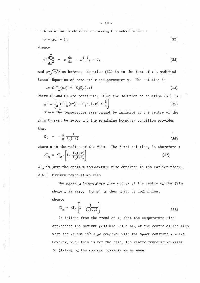
A solution is obtained on making the substitution :
ô = crAT - ß, (32)
whence
)
"r+. r# -r2r2þ=0, (ss)i-Uor
and y=i@< as before. Equation (52) is in the form of tire rnodified
Bessel Equation of zero order and parameter u. The solution is
0= Crlo(ur) + C2Ko(ur) (S4)
where C1 and Cz are constants. Thus the solution to equation (31) is
o, = tr[.1ro(ur) * c2KoCu'l . f] (ss)
Since the tenperature rise cannot be infinite at the centre of the
film C2 nust be zerco, and the remaining boundary condition provides
that
c1
where a is the radius of the filn.
(56)
The final solution, is therefore :
(37)
É_K
AT
ATo is just the optinum temperature rise obtained in the earlier theory.
2.6.1 lt{aximun temperature rise
The naxinum tenperature rise occurs at tire centre of the film
where r is zero. Io(ur) is then tnity by definition,
whence
( 38)
It follows fron the trend of Io that the temperature rise
approaches the naximum possible value ATo at the centre of the film
when tlre radius is''-1arge conpared witli the space constant X = L/v.
However, when this is not the case, the centre temperature rises
to (1-1/e) of the maximun possible value when
ATos
1'l
-l
ro(ua) J
2.6.2
19
I (ua) = e(3s)
2a = 4.5X
Thus the diameter of a circular film should be roughly 1.5
o
times larger than the length of a rectangular strip in order to
reach the same temperature.
Temperature rise near the boundary
In order to conpare the tenperature rise near the boundary
of a circular film with that of a rectangular film, it is convenient
to carry out the substitution :
r=a-Ar
whence
t'AT=AT (40)
o
If we let
¿=çAr
¿tnd
Lr = L/v
thenl- _re(Ej)l (41)AT=ATo.l1L ro(e)
J
From readily available tables for .-? 4çr1 it is easily shown
that
^T+AT.(1-þtÇ>>!, (42)
which is the same result obtained when X=L/V in the theory of
Section 2.5.
This simple treatnent suggests that when the film dianeter
is large compared to the thernal spread constant, the temperature
distribution across the filn is adequately described by one-
dinensional theory. The results of the introductory problem

_20
presented ín Section 2.7 support this conclusion.
2,7 Thermal analysis of a typical thin filn infrared absorber
2.7.L Considerations in the selection of a suitable absorber element
hle have now reached a stage where sufficient theory has been
established to enable us to predict the thermal characteristics of
a thin netallic fitrn upon absorption of infrared radiation.
Initially the author is interested in the selection of an infrared
absorber which would eventually prove suitable for use
in infrared radiation detectors. The final selection of this
absorber element cannot be based entirely on therlnal properties,
as consideration must also be given to other factors such as ease
of preparation, structure, stability and repeatability. An under-
standing of the thermal properties is, however, quite essential
as there are certain fundanental conditions which nust be rnet,
¿¡s hIe have seen in the preceding discussions.
On the other hand, since the conputations must, in the first
instance, be based on known bulk values of thermal conductivity,
specific heat and density, we cannot concede the validity of the
results if these basic properties differ fron the bulk when in the
thin filn forn. The estination of the thermal conductivity and the
product of specific heat and density, from practical measurement of
the thernal rise time and lateral thernal spread, is indeed a most
inportant part of this research project. The results of the thermal
analysis enable us to predict with confidence the conditions under
which these measurements are valid, and conversely, the measured
quantities enable us to make rnore accurate predictions.
In order to illustrate the application of thermal analysis to the
study of thin film infrared absorbers, a problem has been constructed
-21 -
representative of the conditions likely to be encounteled in
practice. It is assumed that this typical infrared absorber
ele¡nent consists of a thin netallic film vacuun deposited on to a
freely-supported plastic filn stretched across a gap in a perfect
heat sink motulted in vacuo. The analysis is divided into three
parts, as follows
(a) The computation of the temperature rise of a rectangular
absorber element when the dimensions are so small that
there is a substantial lateral thernal 10ss to the heat
sink.
(b) The extension of part (a) to a:r absorber of nuch larger
dimensions, typical of the specimens used in the experimental
section of the Project.
(c) A conpari'son between the results of parts (a) and (b)
and the computations for an absorber of circular area and
similar size.
l\Ie will assune in each case that tl're thickness t1 of the netallic
filn is 100R and its enissivity 0"5, and tl'rat the thickness of the
plastic film is 500R. The reason for tlte selection of an
enissivity of 0.5 will become evident in Section 3 of the thesis'
The enissivity of a plastic film of the given thickness is typically
less than 0.02. Hence it does not significantly contribute to the
overall absorption (see also Section 3 .4'2)'
It is also assumed that Kirchoffts Law can be applied (see Section
3.1), i.e., the emissivity of the metallic absorber is equal to its
absorptance. This pre-supposes a Lanbertian radiation lalv, which we
have already assumed in Section 2-l'1"
Gold, nickel and nichrome have been selected for inclusion in

2.7 .2
-)? -
this analysis. These are representativc of high, ntccliunt ¿urcl lotv
thernal conductivity absorber materials. Nichrome is a nickel-
chromiu¡n alloy. The particular alloy chosen for study has the
composition 80Ni:20Cr. A number of netals have in fact been
investigated, but their inclusion in the thernal a:ralysis yields
little further infonnation.
The bulk thernal properties of the selected naterials are
listed in Table 1. The values shown for the substrate rnaterial
are ty¡rical of many thernoplastics.
TABLE ].. BULK THERMAL PROPERTIES OF SELECTED ABSORBER IUATERIALS
0.0022.251.51.5Thernoplasticsubstrate
3.0
0. s95
0.11
2.5
3.87
3.44
0. 130
0 .440
0.420
19. 3
8.3
8.2
Gold
Itlickel
Nichrone
K
IV. (cn. oc) - 1pc
-3oJ. cm c-1
coJ ( c) -l
g
p
-3g. cm
A FORTRAI.¡ program incorporating the thermal equations of the
preceding subsections has been prepared by the author for an I.B.lrl.
7090 Computer. This progran was used to derive the results of the
thermal problem now described.
Incident infrared radiation
Whilst it is not necessary for the purpose of this analysis
to determine an accurate value of the incremental poler, ÀPo,
incident on the infrared absorber, an estimate of the radiant power
intercepted fron a typical source of infrared radiation is of
particular interest. Such an estinate is required in the
experimental investigation of infrared absorption as it enables
-23-
us to predict the rise in absorber temperatuÌe for a given rise in
source temperature.
Let the infrared radiation source be a blackbody Lambertian
radiator of area A situated at a distance R from the absorber
element. Blackbody radiation can be very nearly realised in
practice by means of specially shaped cavities. These cavity
sources are widely used in radiometric research.
If the temperature of the source rises above anbient by an
incrernental amount ATr, then it is easily shown from radiometric
theory that the corresporlding increnlental cirartge in source radiance
at 300oK is given by
aN = 2.02 x 10⁻⁴ lr, (tv.cm-2 sr-1) Gs)
The irradiance at the absorber is
on=þ aN, (w.cm-2; (44)
assuning there is no transmission loss in the intervening atnosphere,
If the absorbe,r elenent is placed in the focal plane of an optical
system of focal ratio Fs, so that the source more than fi1ls the
field of view, then the incremental irradiance at the focal surface
is:
aHo = q (4s)4F o"
where to is the transmission of the optical system.
The absorbed radiant power is
AP = eAHoAs (46)
where e is the absorber emissivity and A, tire surface area. In
practice it beco¡nes difficult to achieve a focal ratio nuch less
than unity. Thus for an f/t optícal systen of transrnission 0.9,
and an absorber emissivity 0.5, the absorbed power is
AP = 1.44x10⁻⁵ eA, AT, (47)

2.7 .3
_24_
for a source at temperature 3O0oK.
Tenperature rise for a small rectangular absorber element
This is part (a) of the thernal problen outlined above. Let
the length of the absorber be 0.1- cn.
The maximun tenperature rise assuming loss of ireat from the
filn by radiation only, is deternined fron ecluations (6), (20) and
(46). Thus :
ATo = 4P76
(48)
For the incident radiant power given by equation (47),
ATo = 0.1176oK (or oC¡
when
AT, = loK
Thus in the ideal situation a rise in source temperature of
approximately 8.soc is required to raise the absorber terpeïatuïe
by toC.
It is important to note tirat the ntaximun tenperature is in-
dependent of both surface area and ernissivity. It also does not
depend on the type of absorber naterial. However, if we are to
observe the rise in tenperature over a reasonable period of time,
then we must seek a sensible thennal response tine. 0n assuming
a lurnped thernal capacitance, equations (L2) ard (26) give the
thermal time constant
. _ PtcltL+?ZcZt2Soetoî:- (49)
where ftc1 and 02c2 refer to the netal and plastic substrate
respectively. Hence we require an absorber film of high enissivity.
However, we cannot infer fron equation (49) which is the best
3ÀHo
SoTo
_25_
absorber, only that it - and the plastic substrate - should be
as thin as possible.
Now let us consider the influence of conduction loss.
The thermal phenonenon which determines the choice of a
particular netal for a small absorber elernent is the lateral
thernal spread. Again assuning lunped paraneters we find fron
equations (13) and (27) that the thernal spread constant for the
conposite film is given by :
X= ttfKztz(s0 )
Thus, as we might expect, the lateral spread of heat is strongly
dependent on the thernal conductivity of the metallic component.
Table l shows that tl're contribution due to the plastic substrate
is small in conparison (provided it is sufficiently thin). Again
we note the dependence on film thickness.
As we have already seen the ternperature rise in the filn does
not attain the theoretical naximurn value ATo unless the length is
large conpared to X. That this is not the case in the present
example is evident from the computation of both the tenperature
rise at the centre of the filn and the average temperature rise,
which are tabulated for the selected materials, together with the
conputed therrnal tine constarts and thermal spread constants, in
TabLe 2. The table shows that only the nichrome absorber,which
has a low thermal conductivity, meets the conditions of equations
(28) and (29). Nichrome is, in fact, a nost useful infrared
absorber, but for reasons IVe will see later, it is not always the
most suitable material.
TABLE 2
26-
COMPI,TTED TIIER¡IAL PARAMETERS
ï xATt/ oto ATaAbsorber (ms) ( un¡ P-/x /No
Gold
Nickel
Nichrome
22.47 70t.2 I.43
3. 18
7 .14
0.2r
0.61
0.94
0.14
0.42
0.72
24.7 3t4 .4
24.00 140.0
Film length
Absorber thickness
Substrate thichness
0. l- cm.
100R
s00R
It is interesting to note that in the absence of the plastic
substrate, i.e., for a self-supporting absorber element, the value of
t is very much snaller (e.g. for nickel it is only 5 ms) whereas the
temperature rise and therrnal spread are essentially unclianged. There-
fore, from the therrnal point of view, the only significant influence
of the plastic support filn is its contribution to the thermal capaci-
tance of the composite fi1n.
The steady state temperature rise along the film, computed frorn
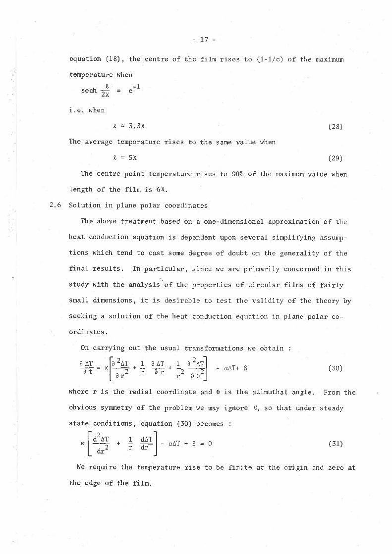
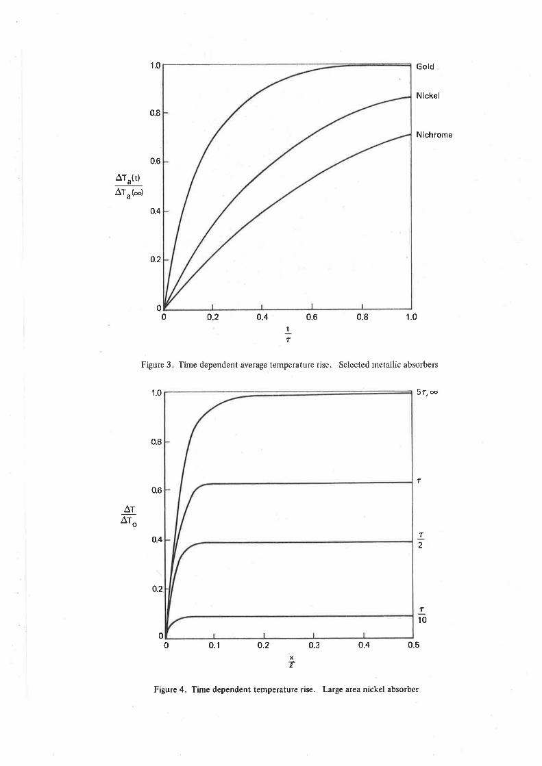
equation (L7) for the three absorber materials, ì.s plotted in figure 1.
These curves readily demonstrate that it is wise to avoid high con-
ductivity metals such as gold unless the absorber dimensj.ons are quite
large; whilst it is almost certainly necessary to choose a low conduct-
ivity material such as nichrome for very sma11 absorbers. 0n the other
hand, another interesting result elnerges when we plot the time dependent
temperature rise (equation 83)). Figure 2 illustrates this computation
for nickel; it shows that steady state conditions are almost realised
when the time exceeds r/2. This is not so for nichrome, as is evident
fron figure 3. Figure 5 shows the time dependent average temperature
rise for the selected netallic absorbers. It is clearly seen that the
0.8
1.0
0.6
o.4
0.2
00.1 o.2 0.3
Nichrome
Nickel
Gold
AT,
aTo
AT
0 0.4 0.5
Selected metallic absorbers
X
T
Figure l. Steady state temperature rise
1.0
0.8
0.6
0.4
o.2
5r,æ
T
T
2
AT
o
T
10
0.1 o.2 0.3 0.4 0.5
xT
00
Figure 2. Time dependent temperature rise. Nickel absorber
Ara(t)
ATa("")
1.0
0.8
0,6
0.4
o.2
Gold
Nickel
Nichrome
00 o.2 0.4 0.6 0.8 1.0
Figure 3. Time dependent average temperature rise. Selected metallic absorbers
5r,æ
T
T
10
00 0.1 o.2 0.3 0.4 0.5
tr
1.0
0.8
0.6
Arar"
T
204
0.2
X
î
Figure 4. Time dependent temperature rise. Large area nickel absorber
2.7.4
-27_
ternperature rise is much faster for materials of higher thernal
conductivity, although the actual magnitude of the ternperature
rise is lower. This result is relevant to the study of infrared
detectors lvhere it is often desirable to sacrifice sensitivity
for speed of response. In sucl"r a case a compromise is necessaly.
Temperature rise for a large absorber element
In this section we extend the above analysis by increasing the
length of the absorber to 1.0 cm. This change does not alter the
values of t and x; however, it is now found that
9" = I4.3X for gold
9. = 3L.8X for nicl<eI, ild
9" = 71.5X for ni-chrome.
Thus in all cases, the tenperature rise at the cerìtre of the film
approaches the theoretical maximum value ATe. The tine dependent
results for nickel are illustrated in figure 4. The absorber is
norv sufficiently large to approxirnate the conditj-ons for an infinite
fi1n, as evident frorn tire observed rise in temperature to (1-1,/e)
of the maximum value in time'r. The temperature will rise to 99.995%
of its maximum possible value in tine 5r and when this condition is
reached the value of X can be read off the x-axis at the (I-|/e)
ordinate.
These results are of particular significance in this project for
it is evident that the thermal time constant can be determined
experimentalLy by a sinple radiometric measurenìent of the temperature
rise at the central region of the fi1m, whilst the thermal spread
constant can be estinated from the output trace of a scanning radio-
neter under steady state conditions. These neasurements in turn
provide data for the computation of the thin filn pc product and the
2,7 .5
_28_
thermal conductivity.
Absorbers of circular area
In concluding this theoretical study rve lìow examine tl-re remaining
variable discussed in Section 2.1, the surface geometry of the
absorber film. Circular elements are widely used in infrared radio-
netry - including the experimental sections of this study, and
hence are of special interest. The above theoretical problern is
readily extended to absorbers of circular symmetry by naking use of
the solutions in plane polar coorclínates derived in Section 2.6.
A direct comparison with the results for a small rectangular stTip
is obtained by selecting an absorber cliameter, 2a, of 0.1 cm. The
steady state temperature rise for the selected absorber metals,
conputer frorn equation (37) , is illustrated in figure 5. It can
be seen that lateral conduction loss is more significant for a
circular filn. In this particular exanple, the naximum tenperature
rise is 56%, 70ro and 92e¿ of the corresponding rise for the recta:rg-
ular film, for go1d, nickel and nichrome, respectively'
As the diameter of the filn increases the ternperature distribu-
tion across the fiLn steadily approaches the one-dinensional
distribution derived in section 2.3.t. lvhen the diameter is 1-.0 cm,
the distribution across the nickel filn is effectively indistinguish-
able fron the curves shown in figure 4, including the region near
the boundary. This result follows directly from the theory of
Section 2.6 .2 .
We are able to conclude confidently that the temperature distri-
bution acïoss a tl-rin filn infrared absorber is essentially
independent of absorber geometry provided the shortest linear
dimension of the film is large compaled to the thermal spread
AT,
a--r;
1.0
0.6
o.2
Nichrome
Nichrome
I.o
Nickel r
Nickel O
I
o
0
Gold
Gold
0.1 0.2 0.3 0.4
Figure 5. Stoady state temperature rise for rectangular and circular absorber elements
x a-r1,Ta
29
constant. Just how large depends on the accuracy required. As
a guideline it is readily shown that the error in the application
of the one-dimensional theory to the solution of the temperature
distribution across a circular absorber of diameter 10X is less
than 2.5eo. This guideline ì-s equally applicable to other
absorber geonetries, such as a rectangular element supported at
each edge when the temperature distribution is cleternined along
the centre line between tne opposing paralleI edges.
3. OPTICAL AND ELECTRICAL PROPERTIES OF TTIIN I.IETALLIC FILI,IS
3.7 Introductory note on radiornetry
In Section 2 we discussed the heating effects of infrared radiation
absorption in metallic fi1ms. The efficiency of energy tïal1sfer depends
on the absorptance of the filrn, whicir lve have assumed to be equal to tl-re
emissivity. This assumption is of fundamental importance in our study ofinfrared absorption, and is a consequence of the application of Kirchoffrs
Law (see, e.g., ref. 4). The laws of radiometry require that the sun ofthe absorptance, o, reflectanc€, Q, and transmittance, .r, be unity, thus:
(l=e
oc+p+1 = | (51)
e=1_(p*r)
tvhere e is the emissivity. In the strict sense we should call this c¡uantity
tlre fremissancerr (see ref. 4) , rescrving the tenn .emissivityr for intrinsicnaterial properties, Ilowever, it is common practice to use I'emissivity,'
for both intrinsic naterial properties and rneasurecl specimen properties.
The emissivity of a plane surface may be expressed in three different
forns 'l
(a) the hemispherical enissivity, measured over the total hernisphere
enclosing the surface;
50
(b) the directional emissivity, measured at some direction to the
surface represented by tl're angular coordinates (0,(r), or
(c) the norrnal enissivity, which is the directional cmissivity
measured normal to the surface.
These may be further divided into spectral emissivity, whereby the
enissivity is measured over a smal1 rvavelength interval of the emission
spectrum and is given a À subscript; and total ernissivity, me¿Lsured over
the total spectral range. The forrner is just the ratio of the spectral
enittance of the surface (radiant power per unit area per unit wavelength
interval) to that of a blackbody, and the latter the ratio of the total
(integrated) ernittance of the surface to that of a blackbody.
In Section 2 we considered only total emissivity. Furthermore, we
assumed the absorber film to be a Larnbertian surface, i.e. a perfectly
diffuse surface with a radiance (radiant polver per unit surface area per
unit solid angle) independent of viewing angle. I.'or such a surface the
henispherical and directional enissivitie-s are equa1. In practice it is
found that the difference betleen the henrispirerical ernissivity and the
normal enissivity is usually sma1l, except for polished metals, where
this difference may be as high as 20%; r,vhilst the variation with angle,
even for metals, does not become significant until the angle exceeds 45o
to the normal.
The hemispherical elnissivity is inportarìt in the calculation of radiant
heat transfer. The normal emissivity, wirich is the quantity usually
measured and quoted, is important in the determination of absorption frorn
distant sources, as in the case of infrared detectors. By definition, the
two emissivities are equal for a Lanbertian radiator, and in practice the
assumption of Lambertian characteristics is sufficient for rnost applications.

3,2
31 -
Electromagnetic theory of the optical properties of absorbing media
The absorption of infrared racliation in thin metallic films can be
adequately described by means of classical electromagnetic theory' The
interaction of radiation with absorbing media of liigh electrical
conductivity turns out to be much sinrplified at far-infrared wavelengths,
and the absorption mechanism is readily explained from rvel1 established
theory (see, e.g. ref. 5). The following brief sumnary outlines the
fundamental concepts.
The wave equation for the electric field E in conducting media is
) ðE à28v'E = ouuo # * .reo luo ;?
(s2)
where o is the electrical conductivity, p the permeability, pe the
permeability of free space, e, the relative perrnittivity or dielectric
constant and eo the pernittivity of free space. The permittivity is
suitably subscripted to avoid confusion with tile enissivity.
If we consider propagation parallel to the x-axis we may write a
solution to equation (52) in the fornNX
E = 9o exp io (t - :.) (53)
where o is the angular frequency, c is the wave velocity in free space and
n is the complex refractive index. By convention we define n as
l=n-ik (54)
where n is the refractive inclex of the rnaterial and k is the absorption
index. substitution of equation (54) into (53) readily yields the
observed experimental law for allsorption (Larnbertrs absorption law) '
Equation (52) is satisfied, provided
n2=n2-k2-2ink.ou1 ---!= tlu eo0
Thus, for non-nagnetic nedia
(ss)
32-
and (56)
2nk = o/eow
The classical theory assunes a continuous mediun in which the dielectric
constant and electrical conductivity both have constant values. This is
not so at high frequencies, whete both quantities are cornplex and
frequency dependent. Thus, by convention, we write the conplex dielectric
constant in the form
1e2
n2-k2-2 ink (s 7)
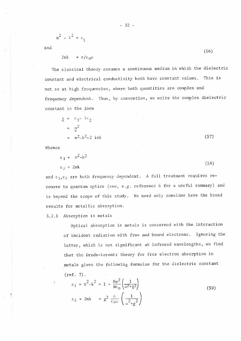
Whence
e I = n2-k2
e2 = 2nk (58)
and e ¡,e2 ãTê both frequency ciependent. A full treatment requires re-
couïSe to quantum optics (see, e.g. reference 6 for a useful sunmary) and
is beyond the scope of this study. tVe need only consider here the broad
results for netallic absorpti-on.
3.2.L Absorption in netals
Optical absorption in netals is concerned with the interaction
of incident radiation with free and bound electrons. Ignoring the
latter, which is not significant at infrared wavelengths, we find
that the Drude-Lorentz theory for free electron absorption in
metals gives the following fornulae for the dielectric constant
(ref . 7).
_ Ne2fleo
o 1
2 ,-2It cn I
c I)
e
n
2 .2n-Ke1 11\
M.-z)
e2 = 2nk o2b E Oú) 22t.¡-l +9
(se)
-33-
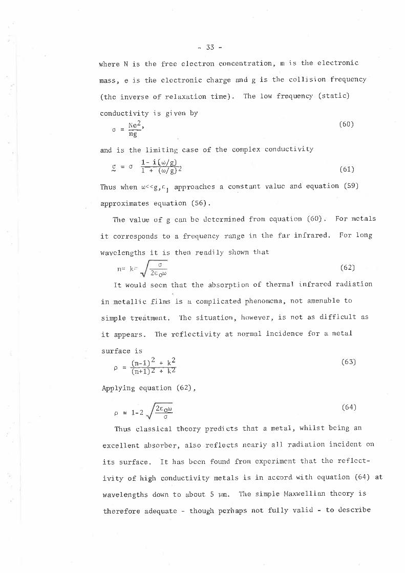
where N is the free electr.on concentration, rn is the electronic
mass, e is the electronic charge and g is the collision frequency
(the inverse of relaxation tine). The low frequency (static)
conCuctivity is given by
Ne2.rng
and is the limiting case of the conplex conductivity1- i(o7g)-^O = O = '',I-+ (u/-fi2 (61)
Thus when o<<g,el approaches a constant value and equation (59)
approximates equation (56).
The value of g can be determined fron ecluation (60). For netals
it corresponds to a frecluency range in the far infrared. For long
wavelengths it is then readily shown that
n= k=o
æ"w(62)
It would seern that the absorption of thermal infrared radiation
in metallic filns is a complicated phenomena, not amenable to
simple treatment. The situation, howevet, is not as difficult as
it appears. The reflectivity at normal incidence for a netal
surface is
- (n- t)2 * k2 (63)- (n+[Z + kZ
Applying equation (62),
g=I-2 2eou (64)
(60 )
p
o
Thus classical theory predicts that a metal, whilst being an
excellent absorber, also reflects nearly all radiation incident on
its surface. It has l¡een found fron experinent that the reflect-
ivity of high conductivity netals is in accord with equation (64) at
wavelengths down to about 5 Um. The simple lt4axwellian theory is
therefore adequate - though perhaps not fully valid - to describe
-34
optical absorption in metals in the infrared at wavelengths greater
than 5 pm. It is not adequate in the near infrared, and fails
conpletelY in the visible.
3,3 Thermal radiation sources
Reference has already been made to the use of "blackboclyrrradiation
sources in this study. The tern 'rblackbody" is of course a theoretical
idealism, but, as noted earlier, such a souïce can very nearly be realised
in practice by means of carefully designed cavities '
1¡is project is concerned with the absorption of therrnal blackbody
radiation from sources near anbient temperature. Tl-Le spectral distribu-
tion of the enitted radiation is given by Planckrs Law and the total
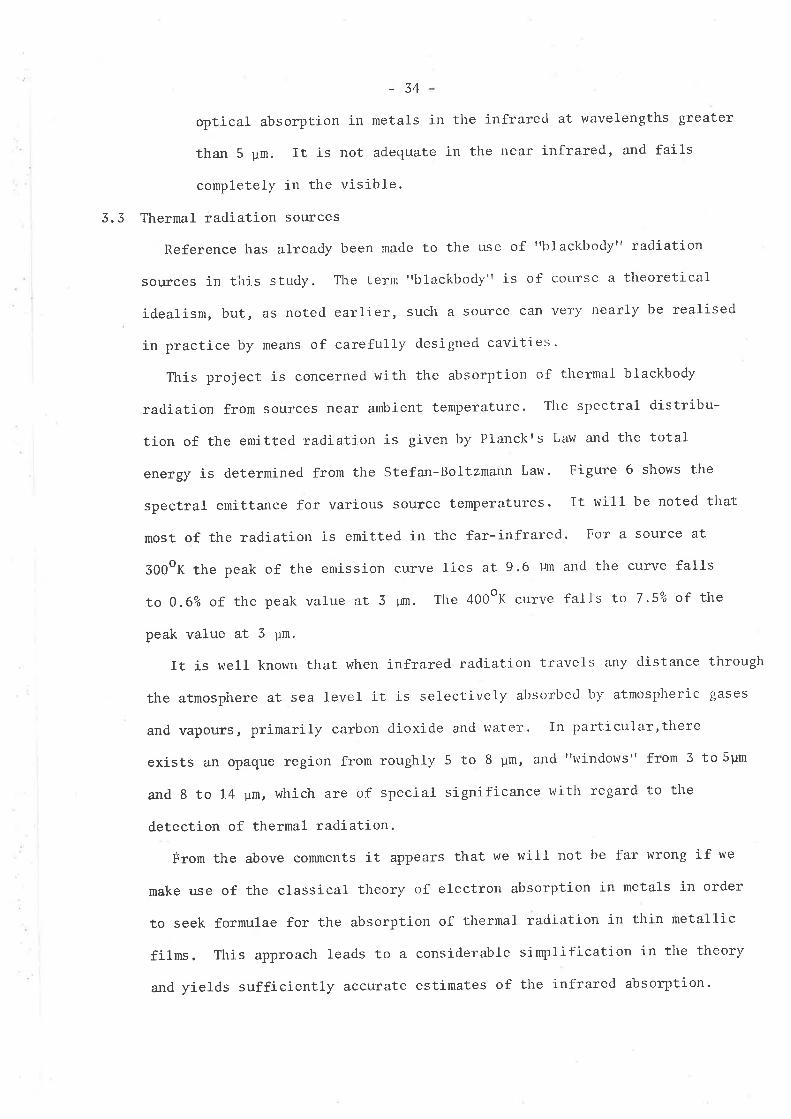
energy is determined from the Stefan-Boltzrnann Law. Figure 6 shows the
spectral emittance for various source temperatures. It will be noted that
most of the radiation is enitted in the far-infrared. For a source at
S00oK the peak of the emission curve lies at 9.6 uln and the curve falls
to 0.6% of. the peak value at 3 Un. The 400oK curve falls to 7.5% of the
peak value at 3 pn'
It is well known that when infrared radiation travels any distance through
the atmosphere at sea level it is selectively absorbed by atmospheric gases
and vapours, primarily carbon dioxide and v¡ater. In particular,there
exists an opaque region from roughly 5 to 8 um, and "windows" from 3 to 5Un
and I to 14 pn, which are of special significance with regard to the
detection of thermal radiation.
Èrom the above comments it appears that we will not be far wrong if we
make use of the classical theory of electron absorption in metals in order
to seek formulae for the absorption of thernal radiation in thin metallic
films. This approach leads to a considerable simplification in the theory
and yields sufficiently accurate estimates of the infrared absorption.

o-21
10-l
10'4
1o-3
E:{d
E(,)
=o)oc(E
.EÊll,lU
(.,0,o.Ø
2 64 IWavelength (pml
10
Figure 6. Blaokbody radiation for three selected temperatures
12 14

3.4
35-
Infrared absorption in thin metallic films
The theory of the optical properties of thin films is well established
and excellent treatises on this important topic are given in various texts,
e.8., the books by Heavens (ref. 8) and Vasicek (ref. 9). This theory
is prirnarily concerned with non-absorbing dielectric fitms. lVe would
expect that the results can be extended to thin absorbing films by the
introduction of the conplex dielectric constalìt. I'his derivation has been
carried out from basic principles in a laborious but excellent paper by
Hadley and Dennison (ref. 10). The results have been checked by the author
of this thesis by the more direct method stated above.
The reflectance and transnittance of a thin absorbing film at nornal
incidence is given by :
p (n2+k2+172 -1
D;
. çn2*u27
4n
4'nlct-T-+4n cosh + 4n(n 4nktsr-nn ---T-
,J | --,- 4nkt --- 4rntlLcosrì À - cos À J
(66)
(67)8"Do
Do= 2+k2*I)
1
14k
ln2*u2*t)2-
ln2*t2 -tlz
where t is the thickness of the fihn and À is the wavelength of the
incident radiation. These equations apply to any absorbing film over the
visible and infrared spectrum. For the special case of a metallic film
in the far infrared, whose thickness is small conpared to the wavelength
of the incident radiation, the above equations, with the aid of equation
.o, $ * 4k(tt2*k2-r) si" S (68)
(62), reduce to the sinple form
p = a2/@+2)2
t = 4/(a+2)2
md, fron equation þ1), we obtain the absorptance (equal
a = 4Q/ (o+2)2 ,
(6e )
to enissivity)
(70)
36
where
-1(
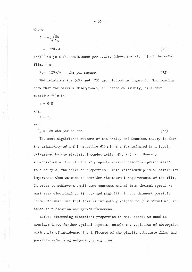
L20not
is just the resistance per square
(77)
(sheet Tesistance) of the metalor)
filn, i.e.,
Rs= t20r/a ohm per square (72)
The relationships (69) and (70) are plotted in figure 7. The results
show that the naxinum absorptance, and hence enissivitL of a thin
metallic filn is
o¿ = 0.5,
when
ó-)
and
Rs = 189 ohrn per square (33)
The most significant outcone of the lJadley and Dennison theory is that
the emissivity of a thin netallic filn in the far infrared is uniquely
determined by the electrical conductivity of the fi1n. Ilence an
appreciation of the electrical properties is an essential prerequisite
to a study of the infrared properties. This relationship is of particular
importance when hre come to consider the thernal requirenents of the film.
In order to achieve a snal1 time constant and rninimum thernal spread we
must seek electrical continuity and stability in the thinnest possible
fi1¡n. IVe shal1 see that this is intinately related to film structure, and
hence to nucleation a¡rd growth phenomena.
Before discussing electrical properties in moie detail we need to
consider three further optical aspects, namely the variation of absorption
with angle of incidence, the influence of the plastic substrate fiLm, and
possible methods of enhancing absorption.
.ã o,aoó
.c¡(E
c 0.6.9o0,
o)
i 0.4o,õ.9EcI o.zF
1.0
010 100
Film resistance (ohms per square)
Figure 7. Infrared optical properties of a thin metallic film
1.0
00 10 20 30
Angle of incidence (degrees)
40
1 000
- o'8.9oo-o(E
i 0.6oo(¡)
o,L
.E o.o
Ø.9EL(gLI o.2
ø
p
T
Film resistance 1 89O/square
Figure 8. Dependence of infrared optical properties on angle of incidence
37-
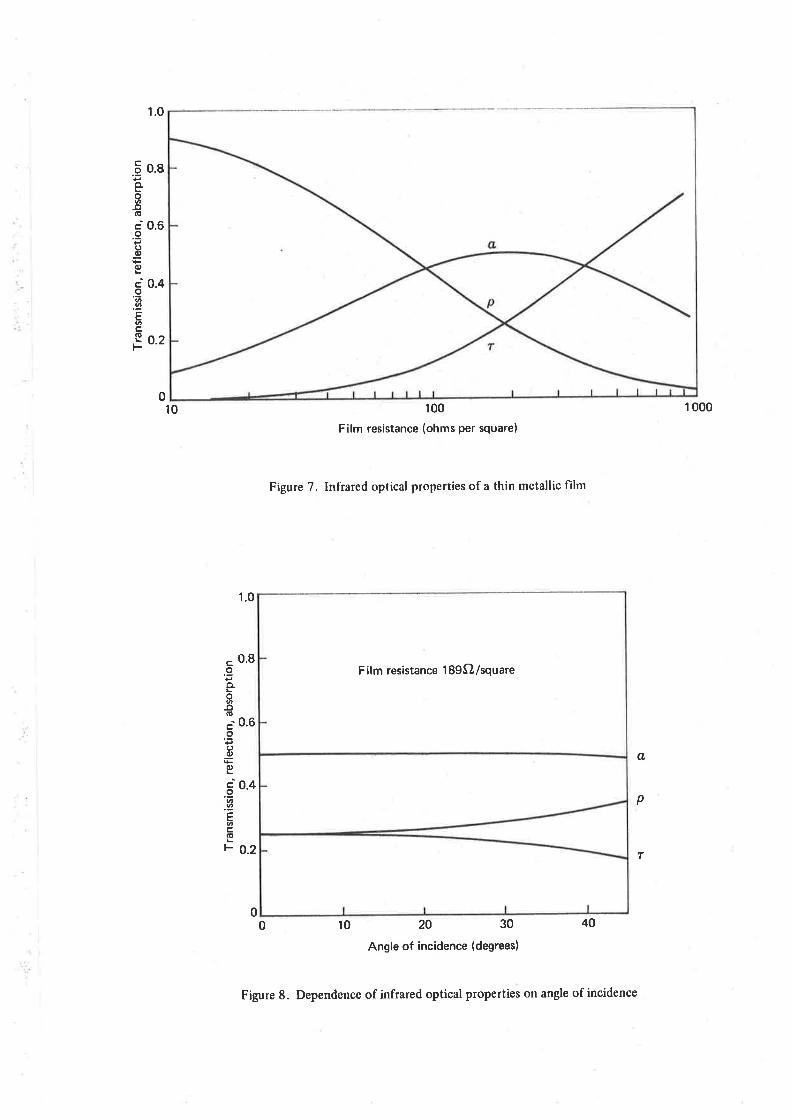
3.4.7 Dependence of absorption on angle of incidence
A firther derivation of the equations for infrared absorption
to include angular dependency leads (ref. 10) to the following
modifications to equations (69) and (70)
a21r - =-õõÃzour'
,--4' - Drcoszo e4)
" = lff=,where 0 is the angle of incidence and
- I 2 o 12Dl = t"""d*.ofü-l tzsl
The graphical results for Q= 2, i.e., for a filn resistance of
189 ohm per square, is given in figure 8. As the angle of incidence
increases the reflectance increases, ild is compensated by a
decrease in transmittance. The absorptance does not vary greatly
from that at nornal incidence (O=0) for angles up to at least 45o,
so that for all practical purposes the angular dependance can be
ignored. This conclusion is in fact substantiated by the optical
measurements described in a later section of the thesis.
3.4.2 Influence of the plastic substrate filnThe theory of Hadley and Dennison has been extended by l{ilsum
(ref. 11) in an effort to seek optimun optical properties for
infrared absorbers used in the Golay pneunatic detector. He
for.tnd that the filn absorption depended on the direction of
incidence of the inconing infrared radiation. When the netallic
absorber filn was deposited onto a dielectric support fil¡n and the
radiation was incident on the surface of the absorber, the absorp-
tance was formd to be
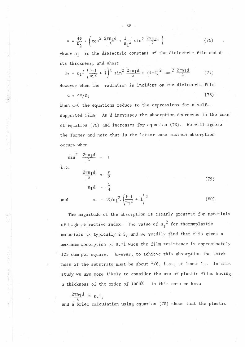
_38_
40 |---z 2rn-tcl . I .n2 UI ) trolo= \. lcos -i-*ñ-r2 tt,. À I
where n1 is the dielectric constant of the dielectric film a¡d d
its thickness, and lvhere
- " /o+1Ur=fl1 Ll-t¿ L
\n1 ',
However when the
o = 4a/D2
\z 2 2tm't d.
/ s1n -i-- Q+2)2 "or2 ry Q7)L
radiation is incident on the dielectric filn
( 78)
When d=0 the equations reduce to the expressions for a self-
supported filn. As d increases the absorption decreases in the case
of ecluation (76) and increases for equation (78). IVe will ignore
the former and note that in the latter case nlaxinum absorption
occtrrs when
. 2 2rntdsin-ï-|
i. e.'r
-')
À
4
= 4o/nr2.(f¿.
(7s)
(80)
The magnitude of the absorption is clearly greatest for naterials
of high refractive index. The value of nr2 for thermoplastic
materials is typicaLJ.y 2.5, and we readily find that this gives a
maxinum absorption of 0.71 rvhelr the filn resistance is approxirnately
125 ohm per square. llolever, to achieve this absorption the thick-
ness of the substrate must be about À/6, i.e., at least lu. In this
study we are nore likety to consider the use of plastic filns having
a thickness of the order of 1000R. In this case we have
2nn-'d-f - u'r'and a brief calculation using equation (78) shows that the plastic
and o¿
')'
3.4 .3
-39-
substrate provides an almost negligible contribution to absorption.
Double netal filn
Interference effects can also be utitised by depositing a thin
metallic filn on both sides of a dielectric film. Maximum
absorption is again obtained in accordance with equation (79). In
this case we have/) t (1+0;a = 4/nf. [1 * '-\nl )
(81)
The highest absorptance is obtainecl for the lowest refractive
index dielectric layer, a maximum of 0.83 being achieved with an
air separation. It is again found that the separation distance is
unrealistic for the experirnents consiclered later in this study.
It is also quite feasible to increase the absorption by deposit-
ing a highly reflecting layer on the reverse side of the plastic
filn, which again needs to be very tlìick - in this case approximately
x/4. In theory, this technique gives almost total absorption.
However, none of the above methods of enhancing absorption are of
practical value in this study because ultrathin films are required
in order to achieve the desired thermal properties.
3.5 Electrical conduction in thin metallic films
It has been shown above that the far-infrared optical properties of
thin metallic films can be adequately described in terrns of the theory of
free electron absorption at low frequencies, the absorption reducing to a
sinple dependency on the low frecluency (static) electrical conductivity.
rt would therefore seem that, at least in principle, it should be
necessary only to deternine the desired thickness of the filn for the
appropriate sheet resistance, in order to optimize the infrared absorp-
tion. Unfortunately the film conductivity cannot be readily predicted,
40-
and in fact the mechanism of electrical conduction in thin films is not
a well understood phenonenon.
The conductivity of an ultrathin fitm in the initial stages of forna-
tion (see, e.g., ref. 14) is nany orders of magnitude lower than the
bulk conductivity. At this stage the film is structurally discontinuous
and charge transfer between rrislandsrr of evaporant is effected by means
of thermionic enission and quantun - nechanical tunnelling. The
conductivity is exponentially dependent on the inverse of the temperature
and is ohnic only for J.ow applied fields. The film is also characterized
by a negative temperature coefficient of resistance.
As the filn becom.es stïucturally continuous the concluctivity increases
dranatically but does not, in general, attain bulk conclttctivity. 'lhis is
due to structural and impurity defects, residual mechanic-a1 stress in the
filn, and scattering fron the film bcundaries. Evert in thick fi1ns, bulk
conductivity is not realised; but it may be closely approached in the
case of low-defect epitaxial fi1ms. In practice it is found that the
conductivity is dependent on evaporation rate, substrate temperature,
type of substrate, degree of vacuum, and contamination, to nane only
so¡ne of the more important factors.
A theory of electrical conduction in continuous nletal filns has been
developedbyFuchs(ref.12)andSondheimer(ref.13).Itisernphasised
that, for the leasons given above, this theory can be used only as a
rough guide to film conductivity. A sumnary is given be1ow. For a more
detailed tleatrnent of this subject, see, fol' example, reference 14.
3.5.1 Theory of conduc't.ion iri continuous netal filnrs
The Fuchs-sondheiner theory is applicable to a defect-free
netallic strip with parallel surfaces. The fal1 in conductivity
with decreased thickness is considered to be due to scattering

4L
fron the film boundary when the thickness' t, becones comparable
with, or less than, the bulk mean free path, Ào, of conduction
electrons in the metal. Tþe scattering is defined in terms of a
Itspecularity parameter.rr, p, which has the extremes of unity for
perfectly diffuse scattering at the film surface, and zero for
specular reflection at the surface. The ratio of the thin film
to bulk conductivity is found to l¡e00
o da, ( 82)oo
where
< = t/xo,
a¡rd a is a dummy variable.
For very thin films, when r<<l- and P' 1 ' this equation reduces to
oo =! 1-n. I , (SS)o-3 Gä@
and for thick films, when K>1,
o^8rc
where both equations are expressed as the ratio of thin filn to bulk
resistivity t/å
The thick filn approxirnation is in fact found to be accurate to
a maximum error of 7% tvhen r is as small as 0.1. The thin filn
approximation often cannot be applied in any case, as the thickness
then corresponds to the region where the film is discontinuous and
conduction takes place by mears of a different mechanism.
The theory may be extended to include the temperature coefficient
of resistance (T.C.R.) of thin metallic fi1ms, where
r.c.R.= -19 (Bs)o ol
The full equation (82) has been evaluated by Soffa (15), with the
13fr (1-p) 1
Ja
1 - exp(-ra)1-p exp(1-rca)
1.-5
aI
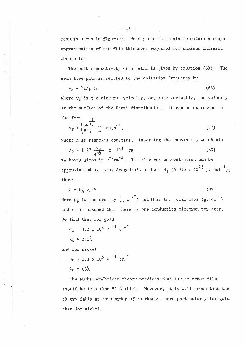
-42-
results shown in figure 9. We may use this data to obtain a rough
approximation of the filn thickness required for rnaximum infrared
absorption.
The bulk conductivity of a metal is given by ecluation (60). The
mean free path is related to the collision frequency by
Ào = vflg cn (86)
where v¡ is the electron velocity, or, more correctly, the velocity
at the surface of the Ferni distribution. It can be expressed in
the form I
"' = (å+)'h -1m cm.s ,
where h is Planckrs constant. Inserting the constants, we obtain
Ào = 1.27 + x 104 cn, (8S)N/J
oe being given in Q-1.r-1. The electTon colìcentration can be
approxinated by using Avogadrors number, NA (6.025 x to23 g' ,nol-l;,
thus:
l.l = N¡ o¡lM
Here o, is the density (g..*-3)
and it is assumed that there is
We find that for gold
oo = 4.2 x 10⁵ n -1 "t-1
Ào = 350R
(87)
(Bs)
and l{ is the molar mass (g.mot-l)
one conduction electron per atom.
and for nickel
oo = 1.1 x 10⁵ n -1 .r-1
Ào = 65R
The Fuchs-Sondheirner theory predicts that the absorber film
should be less than 50 R ttti"L. However, it is well known that the
theory fails at this order of thickness, more particularly for gold
than for nickel.
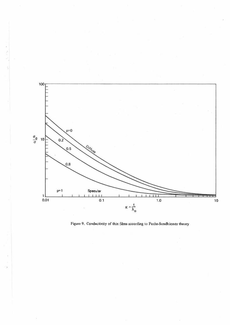
't00
oo ro
o
0.01 0.1 1.0 10tK=L
Figure 9. Conductivity of thin fìlms according to Fuchs.Sondhiemer theory
p=1 Specular
5
o.2
'.\
-43-
Nevertheless in the absence of more detailecl information we
would expect that the onset of gross defects and boundary effects
is urlikely to be significant until r< falls belorv unity, Thus it
would not be far wrong to seeh a t¡ichness of 100 to 200R for gold
and 100R or less
that can be made
for nickel. This is the rnost accurate estinate
at this stage.
we can proceed no further without a more detailed study of the
nucleation and growth Process.
4. NUCLEATION AND GROIVTII PROCESSES AND TIII] STRUCTURE
OF TFIIN METALLIC FILI\4S
4.I Introductory concepts
The physical structure of thin metallic films is of fundanental
importance in this study. It has been shown in earlier sections that a
requírement for low thermal capacitance and minimum thermal spread
demands that the metal absorber filur be as thin as possible. This ultra-
thin filn must then be electrically continuous, and have suitable
conductivity in order to attain optimum infrarecl absorption' It must also
be electrically stable and thcrmally uniforn. In the icleal situation
whi-ch we would eventually hope to achievc, the filn tvould need to be
entirely self-supporting and this, in addition, demands the preparation
of defect-free, structurally continuous films'
The structural characteristics of a thin film are dependent on the
mechanisns of nucleation anci growth during the initial stages of forrnation'
We will see that an appreciation of the physics of these phenornena not only
provides us r,¡ith a guide to film deposition paranteters, but enables us to
predict with reasonable confidence the metals which are most likely to meet
the present requirenents.
4.1.1 AdsorPtion of vaPour atons
Metal atoms thermally vaporized in vacuo inpinge upon the sub-

-44-
strate surface on which condensation is desired with an average
kinetic energy:
n^..=]tr (eo)-av 2
where k is the Boltznann constant and T is the absolute tenperature.
For vaporization tenperatures of L600oK a:rd 1800oK (corresponding
to a vapour pressure of 0.01 torr for gold and nickel) the average
kinetic energy is 0.2ev and 0.23ev respectively.
0n reaching the substrate there are three main alternatives
available to the incident vapour atons (for the following treatment
see also ref. 14)z
(a) reflection
(b) physical adsorption
(c) chemical adsorption
(d) penetration
Let us assume for sirnplicity tl'rat only physical adsorption
takes place - this is reasonable if the substrate is chemically
stable and the kinetic energy of the atons is not too high. The
impinging aton ís attracted by the insta:rtaneous dipole and quad-
rupole rnoments of the surface atoms. This physically adsorbed
atom, called an adatom, diffuses across the surface, hopping from
one potential well to another, and renains on the surface for a
nean stay time:
TE.', = t' exp if- (s1)
'o --rs
where E, is the absorption energl, T, is the sul¡strate teÍPerature,
and vo is the adaton surface vibrational frequency (typicall y L0]-2
to 1015 ,-t). If the adatom does not combine with other adatorns
during its stay tirne it is desorbed into the vapour phase.
-45-
Depending on tire conditions of deposition the adatom may or may
not attain thernal equilibrium. It has been estinated (ref. 14)
that the adatom will lose most of its initial kinetic energy within
2 to 3 lattice oscillations. The relaxation time required to
equilibrate is then given approximately by
- - ): "*o -!g- (92)'T - L,s-^p kT,
An equilibrated adatorn diffuses over a distance
n = z4d "rç æ (s3)
deternined from the Einstein relation for Brownian motion. d is the
junp distarce between adsorption sites and E¿ ís the activation
energy for surface diffusion.
The value of kT, for substrate temperatuÏes up to several
hundred degrees K is typically less than 0.1 ev. The adsorption
energy is trsually much higher, and when this is so we night expect
a short relaxation time. It is found, in general, that E"=4E¿.
It should be noted that in sone cases the avelage kinetic energy
of the incídent atoms is larger tha-n the adsorption energy and all
impinging atoms may not be physically adsorbed. Furthernore thernal
equilibrium may not apply, e.g., when the intpingement rate exceeds
the adatom diffusion rate.
4.1, .2 Initial nucleation
It is well known that the final structure of a thin filn is
strongly dependent on the characteristics of deposition during
initial nucleation. This is a complex process, markedly influenced
' by a number of deposition parameters, and therefore not readily
amenable to analytical treatment. Sevetal theories have been
proposed (see, ê.g., references L4,16, 17r 18, 19). None of these
aïe entirely satisfactory, but are in broad agreement with observed
-46-
phenonena.
The first adatons appearing at the substrate execute a random
lvall< as they diffuse across the surface. If, during the lifetime
rs, given by equation (91), they encoulìter other adatorns, mutual
capture nay occuT with the subsequent formation of an atomic
cluster or nucleus. This nucleus will not be stable, unless the
size of the rcritical nucleusr - usually compOsed of only a few
atoÍrs - is exceeded. Eventually a saturati.on density of stable
nuclei is reached; newly arrived adatoms are then captured by
stable nuclei, and a three-dimensional risland structuret begins
to form.
Let us assune that the substrate is a smooth, inert sutface,
having No adsorption sites per uni.t area. If ttre amival rate of
-') - 1
single atoms is R (atom cn'=-t) t¡en tve might suppose that in
tirne r, the equilibriun population of sir-rgle adatoms would be
li = Rrs (94)
HorveVer when captuïe occuTs the lifetime is less than tr, artd we
are likely to have
N = Rrc (95)
where ts is the mean lifetine before capture'
It can be shown (ref.L8) that above a transition temperature
To, given bY
r_ - z|g-n¿ (e6)'o - kl.n(Neve/R) '
condensation is initially incomplete, i'e', some adatoms are
desorbed. In this case tlÌe saturation density of stable nuclei
N5 = No exp . [-cur-ud)/krsl (e7)
1S
-47-
Below To condensation is rnore conpletc, i'e', al1 adatoms are
captured, and hence all incident atoms will forln stable pairs, with
a saturation densitY4 (e8)
It is of interest here to evaluate To' Let us assume
2Ea - Ed = 1.25 ev,
corresponding to an adsorption energy in the ra:rge 0.5 to 1.0 ev.
For a deposition rate of 1R s-l und an adsorpti-on site density of1c -) 2 -t
1015 cm-Z, ild for a typicat value of vo of 10" s *,
To = 515oK
It rvill be noted that Ts is strongly dependent on the adsorption
energy and hence on the type and physical condition of tl're substrate
surface. It is less sensitive to change in deposition rate.
This sirnplified outline of the initial nucleation plocess
represents an idealised situation. It does not take into considera-
tion some important deposition parameteÏs, e.g, kinetic energy of the
vapour atoms, ffid cannot be expected to account fu1ly for the
observed phenomena. A notable deficiency in the above treatment is
the tendency towards "agglornerationrr (see Section 4.2.1) as the
substrate tenperature increases, with the resulp that the saturation
density represented by equation (97) is not realised. In general,
therefore, we should not expect to find a sl-rarp transition
tçnperature.
,, In sunmary, we night expect that grorvth takes place on an island
structure of density clecreasing with increasing substrate tenrpera-
ture but relatively insensitive to deposition rate. At very high
deposition rates tl-re island density will increase due to the
stlong interaction between incident vapour atoms and hence short
lr,¡on\cNs "* (räFJ.
-48-
lifetime before capture. This is indeed what is observed in
Practice.
Progressive nucleation presupposes a certain degree of super-
saturation. Nucleation theory (refs . 14, 20) predicts that with
increasing supersaturation (higher nelting point materials, lower
substrate tenperatures) a lalge number of smaller sized stable
nuclei are formed.
4.2 0bserved nucleation and growth phenomena
4,2.L Adaton surface mobility and filn aggloneration
A useful qualitative description of nucleation and growth nay
be given in terms of the migration or rrnobility" of adatoms on the
substrate strrface. Adaton surface mobility is found to increase
(a) with increasing substrate tenperature,
(b) rvith films of lorv-melting point materials,
(c) for snooth, inert substrates, and
(d) with an oblique angle of incidence of the vapour stream
A high surface rnobility is observed to give rise to increased
filn ilagglomerationrr. Agglomeration is a descriptive tern for the
tendency to form larger islalds. Iligh agglomeration inplies large
grain size and low island density. The film l¡ecomes continuous
at a higher average thickness a¡rd will have less frozen-in
structural defects. As we might expect, agglomeration increases
with decreasing nucleation density.
Under conditions of therrnal equilibrium we would expect the
adatom mobility to increase with increasing deposition rate and
kinetic energy of the arriving atons. However at high deposition
rates, when the arrival rate is larger than the rate of surface
diffirsion, adatorns react strongly with each other, resulting in low
4.2.2
-49-
surface nigration. An increase in the initial nucleation density
nay also be brought about by the presence of electrostatic charges
on the incident atoms, by the penetration of enelgetic atoms into
the substrate surface, by the influence of adsorbed inpurities,
and by the use of a non-inert physically non-uniforrn substrate.
All of these factors lead to lower agglomeration.
The growth sequence
Initial nucleation cannot be readily observed because the size
of the nuclei is beyond the resolution capability of electron
microscopy. Subsequent growth has however been carefully observed
and recorded in a number of laboratories, the best known published
work being that by Pashley et al (refs . 2I, 22) who observed
growth phenonena within the electron rnicroscope. The generally
accepted growth sequence nay be summarized as follows :
(a) Initial nuclei fornation, as discussed previously
(b) After attaining a saturation density, newly arrived atoms
contribute to an increase in size of the islands, without
any significant increase in numbers
(c) A further increase in size accompanied by a consideral¡le
decrease in island density as the islands coalesce.
This gives rise to
(d) a connected nethlork, usually developing into a channeled
structure, and finally
(e) a continuous, hole-free filn
The coalescence stage has been described by Pashley as trliquid
likerr - although the deposit is certainly not liquid - and it is
observed that the later stage of coalescence is dependent nainly
on the arrival of freshly evaporated ato¡ns. This implies that
4.2.3
-50-
with a high deposition rate there is a rapid ternination in the
coalescence process.
The dependence of fil¡n growth on deposition rate is not always
clear. Thus Chopra (ref.23) has observed that during the initial
growth of gold and silver filns agglomeration increased with
deposition rate, for rates in the range 0.3 to fO Rs-l. This is
contraly to connon belief, for it is usually accepted that grain
size during growth is not strongly influenced by deposition rate
except when the deposition late is very high.
Chopra also noted that for a fixed deposition rate aggloneration
increased with higher evaporation rates, i.e., kinetic energy of
the vapour atoms, Whilst thls may be so for a given rnetal, the
size of stable nuclei is small for high nelting point netals and
hence the island density shorrld be high for these netals. It is
well established that fine -grain deposits are indeed obtained for
such metals as platinun, ni cllel, chromiun, tungsten and moLybdenun.
Film structure
It has been noted above that fine grain deposits are to be
expected hrith high melting point naterials and for high deposition
rates and low substrate tcrr4tcratures. Filns deposited under these
conditions are nore likely to attain structural continuity at a
lower average thickuess than highly agglonerated filns prepared at
low deposition ratei and high substrate te͡peratures. However the
filns would probabl¡ have a greater number of frozen-in defects.
Filns deposited onto anorphous substrates are generally
polycrystalline, regardless of substrate temperature. Epitaxial
growth r-r.sually requires a single crystal substrate (cleaved rnica,
NaCl, MoS, etc.) with deposition at an elevated substrate tenpera-

4 .2.4
-s1 -ture. The higher substrate teTnperature also reduces defects
and assists in removing substrate contamination; factors which,
together with a contamination-free vacuum environnent, are essential
to high grade epitaxy.
An interesting grorvth pattern nay be observed when the substrate
surface has a rough, granular or porous texture. Alumina sub-
strates fall into this category. A surface of this type should
give rise to a fine-grain deposit due to low adatom nigration.
However a heavier deposit is needed to obtain structural continuity
due to the greater effective surface ar.ea and the penetration of
vapour atoms into the porous structure. We may well expect a
similar situation with plastic substrates, as the physical structure
of these materials would tend to suggest extensive penetration,
especially for high rnelting point evapolants. This penetration has
been observed by the author and is described in a later section of
the thesis.
Many authors have noted that the structure of filns deposited
on to different anorphous substrates (e.g. glass and plastic), and
under the sarne deposition conditions, is of similar texture.
Substrate transition temperatures
It is clear that the temperature of the substrate has a marked
influence on the growth process. How general this influence should
be is not readily obvious, as growth is also strongly dependent on
other paraneters; although we do know that a higher substrate
temperature increases adatom rnobility and encourages aggloneration,
and is essential for epita4r.
Russian investigators have observed a relationship between sub-
strate tenperatule, crystalline structure, and the bulk nelting
-52-
point of the netal. Their observations appear to apply to a wide
range of metallic evaporants.
The Russian research is sumnarized in references 24 and 25. The
essential results of this work are that three broad regions can be
identified which are directly related to crystalline structure as
a firnction of both substrate temperature, Ts(oX), and the melting
point of the evaporant, tr(otr). These are as follows :
)(a) Tr> ! T* : In this region film condensation occurs via a
vapour + liquid + solid transformation. During initial forma-
tion the deposit consists of large, spherical crystallites
which are sometimes faceted. The region extends to the so
called ilcriticalrr temperature, above which condensation
cannot be observed.1)(b) å t, -. T, .< ! T* : Condensation occurs via a vapour + solid
transformation. For amphorous substrates the crystallites are
large and flat, with smooth or faceted outlines. This is the
region favoured for epitaxial growth. The use of single
crystal substrates affects the results, in particular by
extending the region to higher temperatures.1(c) T, e ! T,n : Condensation is via a vapour + solid transforma-
tion, and there is evidence in some cases of the transforma-
tion vapour + liquid + solid. Crystallites are rninute
rdropletsr, sometimes too sna1l to be resolved by electron
nicroscopy.
The above suppositions are in, general agreenent with published
descriptions of film formation. Perhaps the best corroborative
example is the extensive work reported by Pashley et al (refs. 2L,
22) on epitaxial filns of silver and gold, which were deposited on-
_53_
to single crystal substrates at a temperature of 350oC.
Further evidence of ternperature transition regions is to be
found in early papers by Levinstein (ref, 26) a¡rd Sennett and
Scott (ref. 27), ín both cases relating to room temperature
anorphous substrates. In general, it was found that fine-graíned
structureless deposits were obtained rvith high nelting point
netals, the crystallite size progressively increasing for lower
nelting point metals, in broad agreement witl'r the above predictions.
Rapid evaporation also accentuated the formation of rraggregatedil
deposits.
4.3 Electrical conduction
The preceding discussion on the fornation and structure of thin films
can leave no doubt as to the fundamental significance of the nucleation
and growth process to electrical conduction in this metallic filns. During
the early stages of formation conduction tahes place by nears of thermionic
emission and ttmnelling between islands, the forrner being favoured for
larger inter-island spacing. The substrate has an additional influence
as it is now widely believed that electron transfer for the barrier
mechanisns takes place via the substrate.
4,3.L Final filn resistance
The bridging of islands during coalescence is acconpanied by a
dranatic i-ncrease in conductivity. As we have seen, the average
thickness at which this occurs - called the "critical thicknessr' -
is strongly dependent on deposition pararneters. It follows that the
final resistance of a thick continuous film also depends on the
conditions of deposition.
Filns deposited on to room temperature substrates are observed
to have a higher resistance than films deposited (on to the sane

4 .3.2
-54-
substrate) at a higher substrate tenperature; although in the
latter case the decreased resistivity is achieved at a greater
final thickness (see e.g. chopra et aI, reference 28). An increase
in substrate tenperature above a certain value typical of the
naterial will be accompanied by a sharp rise in resistance. This
effect is discussed in Section 4.3.2.
The textr¡re and condition of the substrate surface also has a
narked influence on final resistance. The resistance of a filn
deposited on to an alumina substrate is typically twice as high
as that for a glass substrate under identical evaporation conditions '
The author has also observed a higher resistance for films deposit-
ed on to polyrner substrates .
Chopra and co-workers (ref. 28) have found that the resistance
of sputtered gold fílns is lower than that of thermally evaporated
filns, and in each case epitaxially grown films prepared on heated
(mica) substrates had a lower resistance than polycrystalline filrns
deposited on to cold substrates - substantially in agreenent with
the abovementioned tendency. The critical thickness was much
sharper for the epitaxial films. These results are in accord with
the observations of other authors; however the nethod of evapora-
tion is evidently important as the resistance of filns has been
elsewhere reported to be lower for thermally evaporated filns than
for sputtered filns.
Aging effects
Tlte resistance of continuous metallic films deposited on to room
temperature substrates usually decreases with time, beconing stable
after several hours. This aging effect can be accelerated by baking
the film, and subsequent cycling below the aging temperature

-55-
generally induces no resistance instability (i.e. the filn
resistance is reversibte). A decrease in resistance after deposi-
tion nay not occur with unstable or cirenically reactive naterials -
Ihe author has noted an increase in resistance with aging for
nickel and nichro¡ne filns, evidently due to oxidation. The aging
of nichro¡ne filns can again be accelerated by heating, and aged
films are renarkable stable. In other cases an increase in
resistance can be traced to substrate heating during clepcsi-ti'on'
Belser (ref, 29) has described the effect of thermal aging on
a number of metallic films, which were deposited on to glass
substrates at room temperature by neatrs of both thernal evaporation
and sputtering. Belser postulates that there is a preferred aging
tenperature for each rnaterial, rvhich is clepenclent on filn thickness
but closely associated with the recrystallization temperature of
the netal. The aging plocess assists in the removal of strains
induced in the filn during deposition, Temoves adsorbed and
occluded gas and promotes growth in the size of crystallites. Aging
at the preferred temperature can reduce film resistance to between
25 and 50% of the rras-deposited'r resistance. The change can be
even higher foÏ ultrathin fiIns. However heating to higher
tempeTatures causes a sudden rise in resistance due to film aggrega-
tion. Aging is nore pronounced rvith sputtered filns, but the
preferred temperature is higher than that required for therrnally
evaporated films.
Belserrs results are essentially in agreement with the observa-
tions of ïnost investigators and help to explain anonalies reported
in the literature. The prefelïed temperatures and resultant cryst-
alline structures ale also much as we would expect from our know-

56-
ledge of the grovltlì process. However it is enphasised that the
growth process during post-deposition annealing is different from
that which occurs at the sane temperature cluring initial fornation.
Aging of metal filns can also be accomplished by passing an
electric current through the fi1n. This method has been used
extensivety in the author's laboratory, particularly for gold
filns deposited onto plastic substrates, where thernal aging is
imprq.ctical.
4.3,3 Electrostatic chalge effects
It was noted earlier that the presence of electrostatic charges
on incident atoms contribute to an increase in the initial nuclei
saturation density, with a subsequent reduction in aggloneration.
Electron irradiation has a similar effect. Several authors have
also noted that the use of measurement voltages during deposition,
e.g., for monitoring filn resistance, influence the growth proces-s
a¡rd in sone instances the field in the vicinity of crystal-controlled
thickness monitors has been known to distur'b th.e vapour stream.
The influence of electrostatic fields applied during the deposi-
tion of silver a:rd gold has been extensively studied by Chopra
(ref. 30). He applied a d.c. field of up to 150V..t-1 in the plane
of the filn and observed a marl<ed influence on the grorvth process.
This field was detrinental to sputtered films due to nodification
of the glow discharge. However for therrnally evaporated films
the field induced coalescence of the island structure at an earlier
stage of growth than is nornally observed. The effect was more
narked at higher substrate temperatures, atthough, as l^ie would
expect, the film resistance for a given thickness was higher.
Continuous films deposited under an applied field were lower in
_57_
resistance than those obtained without a fíeld, a consequence of
recrystallization and reorientation of nuclei during the coalescence
phase. The field is only effective before and during coalescence'
For gold and silver it appears tl'rat the electrostatic field
- effect is not very significant for room tenperature substrates.
This may not be so for lower nelting point netals. On the other
hand, high melting point metals such as nickel, chroniurn and
platinum might not be influenced by applied fields up to quite
high substrate temPeratures.
Aging and electrostatic effects clearly nerit further considera-
tion in the atternpt to prepare ultrathin, stable infrared absorbing
filns.
4,4 Selection of suitable netals for thin filn infrared absorbers
The foregoing description of nucleation and growth in netallic films,
and the dependence of these processes on various deposition parameters,
is substantiated by the vast majority of published work. Considerable
thought has been given by the author to these factors in the search for
suitable naterials and appropriate nethods of preparatibn of ultrathin
infrared absorber fi1ms. Considerations leading to the final selections
are discussed below.
The essential specifications for the desired netallic filn are :
(a) physical continuity in the thinnest possible film achieving
maxi¡num absorption; defect free
(b) Electrical surface resistance of approxinately 200 ç¿ per square
in the thinnest possible film
(c) Electrical stability and thermal uniformity
(d) Chenical stabilitY
(e) Ease of preparation, and repeatibility

58-
(f) Low thernal conductivity
(g) Preparation on therrnoplastic substrates
Plastic substrates are particularly useful for research purposes as
they facilitate ease of measurement of thin filn paraneters. They are
also of some interest as support filns for infrared detectors. The use
of thermoplastic substrates does,honever, place a restriction on the
range of substrate tenperatures which can be employed. We therefore
have the additional specification :
(h) Maxinun substrate tenperature generally less than 150oC.
Evidently hte must seek a metal which forns a stable, low resistance,
microcrystalline filn on substrates near room tenperature. The filn
would probably be formed at high deposition rates to induce rapid
coalescence and reduce contamination. Room tenperature deposition may
lead to excessive filn defects, so that an aging cycle would appear to be
essential. Consideration might also be given to the possibility of induc-
ing early coalescence with the aid of electrostatic fields.
In the first instarce it would seem reasonable to reject all netals for
which the value Tn/S (see Section 4.2.4) is less than, sãy,450 to 475orc.
We thus exclude rnetals with a nelting point of less than about 1350oK.
These metals are usually agglonerated to a gïeater oï lesser degree and
are often electrically or chenically unstable. In the rtransitiont region
we have such metals as silver, copper and gold. These have been rejected
on the basis of known structural characteristics, high thermal conductivity
and (except gold) chemical or electrical instability in thin film forn.
In the high melting point range we need to consider such metals as nickel,
titaniwn, palladiwn, platinum, iron, chronium, etc., and the refractory
metals tungsten and molybdenum. Many of these were discarded because of
their high thernal conductivity or tendency to oxidize and, in some cases,
59-
known difficulty of preparation. Of the renainder, nickel was chosen
for detailed study. Less extensive experiments with gold and a nickel-
chroniun al1oy are also reported in later sections of the thesis. An
initial evaluation of chromium and platinum films was carried out.
It is of interest to note that gernanium and silicon form anorphous
filns on room temperature sul¡strates. These netals cau,however, be
irunediately rejected becatxe of high electrical resistivity and hence
low infrared absorption. They are in fact used as window materials
in the infrared.
4.4.L Gold films
Gold would appear to be eminently suitable because of ease of
preparation and chenical inertness. Gold films have in fact been
used extensively in the authorts lal¡oratory as infrared absorbers.
However, there is abundant evidence of structural non-unifornity
in films of thickness suitable for infrared absorption (see e.g.,
ref. 22), and a careful aging cycle is required to reduce electrical
instability. The thermal conductivity of gold is also high. To
some extent the ain of the present research project is to replace
gold with a superior absorbing netal. It was therefore considered
desirable to prepaïe gold absorber filns for comparison with films
of higher nelting point netals.
4,4.2 Platinun filns
There is anple evidence in the literature (refs. 25, 26, 29, 3L,
32) of the ultra-fine grain, unifonn textuTe of platinun thin
films, regardless of substrate type and for substrate teÍperatures
in the ra¡ge 77oK to 600oK. Platinum is also chemically inert and
therefore, like gold, not susceptibte to reactive contarnination
dtring or after deposition. Its thernal conductivity is also nuch

4.4.3
4.4 .4
-60-
lower than gold. Platinum can be deposited using electron beam
evaporation apparatus .
Our assessment would suggest that platinun is perhaps the ¡nost
promising ¡netal for investigation as a thin filrn infrared absorber.
Palladiu¡n is an alternative metal worthy of consideration.
Unfortunately, initial experirnents with platinun have indicated
certain technical linitations in the deposition process, primarily
concerned with darnage to the fragile polymer substrates. The
author has little doubt that these difficulties can be overcome.
However, in order to satisfy the broad ains of this project, it
seemed expedient to investigate a netal having a lower melting
point than platinun but retaining rnost of the desired characteristics
listed in the foregoing specification.
Nickel filns
Nicke1 is also known to form fine grain deposits (refs , 26, 27
33, 34). Preparation in high to ultrahigh vacuo is required to
avoid oxidation (ref. 34). The thermal conductivity of nickel
is lower than platinun, favouring decreased lateral thermal spread.
Nickel is readily evaporated fron a resistance heated twrgsten
helix or from an electron beam deposition source.
It is worthy of note that both nickel and platinun filns are of
interest as the sensitive elenent of infrared boloneter detectors.
Alloy films
Initial work in this project rvas carried out using nickel-
chroniwn a11oy (nichrome) films, primarily for the purpose of test-
ing apparatus and validating measurement techniques. Nichrome is
also a useful thin filn absorber material. It can be deposite<l as
an extremely thin filn and has a very low thernal conductivity.
-61
Nichrone filns are stable after aging, and tlris factor, together
with a low temperature coefficient of rcsistalcc, favours applica-
tion as a resistive element in thin filn microcircuitry. However,
because of its low tenperature coefficient of resistance, nichrome
is not suitable for use as a boloneter detector.
Experimental studies on nichrone filns are also reported in later
sections of the thesis.
5. PREPARATION 0F I'ÍETALLIC FILI\ß
5.1 Vacuum coating unit
ïre high vacuun coating unit used in this project is illustrated in
figure L0. It is a research orientated system constructed in the authorrs
laboratory specifically for the preparation and systematic study of thin
metallic filns. The punping unit consists of an Edwards type 403 4-inch
(10cm) oil diffusion punp, backed by a 200 [.min-1 two-stage Gaede rotary
punp. The diffusion punp is charged with Dow-Corning type 705 silicone
oil. The chanber pressure achieved during deposition cycles is 2 x l-0-6
torr, neasured with a calibrated Penning gauge. A dual Pirani gauge, with
heads fitted to both the foreline and vacuum chamber, is used for the
measurenent of high pressure. A water-cooled I'cold cap" is fitted to the
diffusion pump to reduce backstreaming.
The vacuum chamber is supported on a l2in (30cm) diameter stainless
steel service ring fitted with 10 standard lin (2.Sctn) dianeter vacuum
ports. The vacuum ports provide cl'ranber entry for electrical leads ard
external nechanical controls. All baffle plates, supports and shutters
within the vacuum charnber are prefabricated from stainless steel. Chanber
components are dremically cleaned and degreased at regular intervals to
reduce contan:ination. Viton elastoner vacuum seals are used throughout.
The vacuum coating unit is located in a clean air environment and the
I
9=6 o cG-
a-¡
!-
o a
3g
I
ú^
' o^nf,u* . C-)::t,:t
-&t&a¡'
-!-
Figure 10. Vacuum coating unit
Neg. No. N73/633

-62-
backing punp exhaust is vented to the external atnosplrere.
Several safety features were incorporated in tlie coating rmit to provi<le
protection during prolonged ar1d unattended pumping cycles. A flow
switch fitted to the diffusion purnp water cooling line actuates a solenoid
valve when the flow rate fal1s below a preset level, cutting off water
flow to the purnp. The flow switch also isolates the diffusion punp
circuit. Protection against a dfop in chanber pressure is effected by a
vacuun switch, which is actuated at 5 torr. This switch controls both
the diffusion punp circuit and the high voltage supply used for gas dis-
charge cleaning and electron beam evaporation. A "m¿urual" bypass circuit
is incorporated to allow the diffusion punp to rernain operative during
vacuum recycling.
5.1.1 Ancillary coating unit
. A general purpose coating unit tvas used for the preparation
of thin film electrical contacts and mirror coatings, and for the
deposition of silver layers required in rnultiple bean inter-
feronetry. This unit rvas also used for pilot experirnents on
nickel, chromiurn and gold absorber films. The attainable vacuun
is better than 1 x 10⁻⁵ torr.
5.2 Deposition control techniques
The conditions of vacuum deposition may be expected to have a marked
influence on the optical and ther¡nal properties of thin metallic filns.
This conclusion was reached in Section 4 fron a study of nucleation and
growth phenomena. It is thus desirable to maintain an accurate and
effective control of the deposition process. In this project electrical
film resistance, filn thickness, deposition rate and chamber pressure
were continuously monitored. The experinental procedure is described
below. Control instrunentation is shown in figure 11. The monitor

Neg. No. N731632
Figure 11. Deposition control instrumentation
63-
circuit is iLlustrated schematically in figure 12.
5,2.L Filn resistance
Electrical resistance rrras nonitored during deposition using a
sinple two-probe measurement technique. The substrate was coated
with suitably shaped evaporated gold contacts. Electrical connec-
tion was ¡nade to the gold electrodes by means of 1nm x 0.025nm
nickel strip sealed to the gold with conducting epoxy cement. After
testing a nunber of silver-loaded epoxy resins, Epo-tek type 410LV
was finally selected for this application. The nickel strips were
connected to tinned copper leads using Canon gold-plated pin
connectors. These leads were insulated with woven fibre glass
sleeving to reduce outgassing. A high vacuum leadthrough in one
of the chanber ports provided aÇcess to the external neasurement
circuitry.
TWo methods were employed for the measurement of filrn resistance.
In the first of these nethods resistance rvas measured directly on
the Ohnmeter ranges of a Keithley Model 610C electrometer. The
electrometeï recorder output was connected to a Rikadenki Model B-54
three-channel potentiometric pen recorder. A precision decade
shunt, connected to the electrometer via a terrninal box, was used
as a resistance leference.
The above direct nethod was replaced during the latter stages of
the research prograrn by a nore sophisticated me¿rsurement technique.
A test current was supplied to the nonitor substrate fron a constant
cu:rent voltage source and the resistance deternined by neasure-
ment of the voLtage drop across the specimen. In this arrangement,
illustrated in figure L2, the electroneter was used as a voltneter
and deposition nonitor. A calibrated resistance reference was
Penninggauge
control unit
Ouartzcrystalmonitor
Electron beam
deposition filamentand HT supply
RecorderChannel 3resistance
Load Ref
0 - 100vRecorderChannel 2
thickness
RecorderChannel 1
vacuum
Figure 12. Monitor circuit schematic
5.2.2
-64-
incorporated within the voltage supply unit and was adjustable in
10 A graduated steps frorn 0 to 10kCI. Two test channels are available
enabling a second specimen to be nonitored during the sarne
deposition. This facility was used to çompare the resistance of
films forned on different substrate materials.
The standard test current was 10 uA. This value vlas selected
as a suitable compronise between measured voltage and permissible
Joule heating of the substrate. Prior to deposition the electro-
meter and pen recorder were calibrated and the voltage source
set to LOAD, with the reference adjusted to give a suitable ful1
scale neter reading, usually lkfl corresponding to a voltage drop
of 10nV. In this position the resistance nonitor slide was wired
in paralle1 with the reference. During deposition, when the
meter reading dropped to nid sca1e, the voltage source was switch-
ed to ffiÆ, thereby renoving the reference resistance from the
circuit. The electrorneter and recorder then indicated a linear
neasurement of filn resistance. This technique also provided a
permanent record of the resistance calibration.
Deposition rate and'filn thickness
Deposition rate and film thickness were nìeasured with a quartz
crystal thickness nonitor. An Edwards Model 1 nonitor was used
for tho deposition of nichrome, nickel, chronium and gold. This
r.¡¡tit was replaced by a Toyocon Model TVF-I monitor for a series
of precision-controlled nickel evaporations. The Toyocom monitor
is more suitable for research applications because of its higher
stability and extended range capability. Both units nake use of
the shift in resonant frequency of an AT-cut quartz crystal to
measure nass and hence thickness of the deposited fi1n. It can be
-65-shohrn (ref . 35) that the filrn thickness, t, is related to
frequency shift, Af, by the formula
f,= lq (ee)
where fo is the resonant frequency (Hz), p.l it the density of the
-?quartz crystal (2.65 g.cm-"), p is the density of the evaporant
(g."n-") and dO is the crystal thickness (cn). It is assumed that
the electroded area of the crystal is unifornly coated with the
evaporant naterial. For the Edwards nonitor
fo = 6WIz,
and dO = Q. 279nm,
... r = r.2S Lr/p 8. (994)
For the Toyocon monitor
fo = SMHz'
and dO = Q.534mn,
f, = r.77 Lf /p R. (998)
In practice, the value of p is uncertain, and the monitor is
usually calibrated for each evaporant using an absolute thickness
measurement technique. Multiple bean interferometry was used in
this work.
During deposition the frequency shift was continuously displayed
on the Rikadenki reÇorder. A deposition rate recorder-output was
also available fro¡n the Toyocom nonitor. However, rate was
usually observed directly from the monitorfs rate meter and checked
by conputation fron the frequency shift traces.
Chamber pressure
The Penning gauge ouptut t^/¿ts connected to the third channel of
the Rikadenki recorder, providing a continuous record of chanber
pd x10B Rq
5.2.3
5.3
66-
pressure during deposition. Recorder outputs were also available
frorn the Pirani gauge units; these we1.e occasionally used to
monitor outgassing cYcles.
In some instances, when it was desirable to nonitor an additional
deposition paraneteï, e.g., rate of deposition or a second resis-
tance neasurenent, the chanber pressuae was recorded on a Goerz
Minegor Type RE501 potentionetric recorder.
5.2.4 Deposition tine
An event marker is fitted to the Ril<adenlci recorder. This lvas
actuated at the commencernent ancl conclusion of deposition, coincident
with the opening and closing of a nechanical shutter interposed
between the evaporant and substrate.
Substrates
It is obviously desirable to prepare all of the filn sanples required
for a particular series of measureïnents during a single deposition' To do
so ensures that there is a unique relationship between filn thickness,
structule, resistance and the rneasqred optical and thernal properties'
This requirenent was achieved as follows.
Substrates were mounted on a 9in (55cn) diameter 1-6-gauge stainless
steel support plate. The substrates weïe arranged within a 7'Scn
dia¡neter circle at the centre of the support plate, imnediately above
the evaporation source. It can be shov¡n (ref. 36) that the thickness,
t, at a dist¿ulce, r' from the celìtre of the plate is
t = roþ+(r/h) 1-Íz (1oo)
where h is the ve1'tical dista¡rce from the vapour soulce to the centle
of the plate and to is the thickness at the centÏe of the plate. This
equation applies for a point evaporation soulce, ild represents the worst
practical case. Greater uniformity is achieved with an extended source,

67-
such as a resistance heated tungsten filanent. Inserting 1. (3.75crn) and
the evaporation distance, h (20cm), we obtain
t = 0.95 to
Thus the maximurn thickness variation is 5%. In practice the variation
is nuch less, both for the individual substrates and from substrate to
substrate. The rnaximum substrate size was 2.5cn diameter ancl substrates
were arranged on a circle about the source, thereby ensuring uniformity
between specinens.
The substratç arrangement for a typical nickel evaporation is illustrat-
ed in figure13. The substrates are nounted in holders fitted to the
support plate. The holders can be re¡noved to facilitate substrate
preparation and assembly in a laminar flow work station. The function of
the various substrates is described below.
5.5.1 Resistance neasurement
Two types of substrates were enployed for resistance measurements.
(a) Glass substrates :
25mm long x 12.Smm wide glass substrates, having a standarci-
ized electrode geonetry, were prepared in large batches and
used extensively throughout the research program. One of these
substrates was inclucled as a reference in most depositions.
Soda-1ine glass uras used for routine measuïenents; borosilicate
glass was preferred for accurate measurements because of its
superior chemical stability. The substrate was nasked to
expose a 6.25mn wide strip to the evaporant, oriented at right
angles to the gap between the gotd contacts, and the resistance
element hras a 6.25mm squaïe, defined by the gold contacts. The
resistance was thus measured directly in ohns per square. The
substrate was spring loaded in the substrate holder (see figure
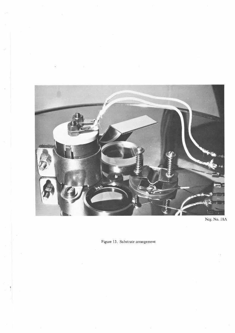
Neg. No. l8A
Figure 13, Substrate arrangement
6B-
13). The holder tvas machined from cast epoxy resin.
(b) Polymer film substrates
Substrates were prepared with various electrode geonetries,
depending on requirements for thermal neasurements (Section
5.3.6). It is important that measurements of resistance be
carried out on filns deposited on to plastic substrates
because these substrates were used for the measurement of
optical and therrnal properties, and there is reason to suspect
that the resistance may differ for various surface structures.
5.3.2 Thickness monitor sensing head
The sensing head was clamped to the support plate with the
qrnrtz crystal elernent exposed to the vapour stream and positioned
at the same evaporation distance as the other substrates (see
figure 13).
5.5. 3 Thickness measurement
A 25n¡n dianeter x 6.25mm thick glass disc, ground and polished
to one fringe on the face exposed to the evaporant, was rnounted
in a precision-machined brass substrate holder, as shown in
figure 13. This holdeï was shaped to expose only one half of the
disc to the vapour stream.
After deposition the disc was coated with an opague silver
layer and the film thickness was determined by nultiple bearn
interferonetry. This neasurenent was also used to calibrate the
thickness monitor.
5. 3.4 Infrared neasurements
The substïate consisted of a thin self-supporting plastic film
nounted on a 25nm o.d., 20mn i.d. aluninium annulus. This
nounting ring was of a standardized design to match the work

69-
holders of various infrared instrunentation. The holder for the
mounting ring was precision-nachined brass. The entire substrate
surface was exposed to the evapolant. One such substrate is
illustrated in figure 13.
The preparation of the plastic filns is described in Section 5.4.
The films have a high infrared transmission and low emissivity and
are therefore particularly suited to neasurement of the infrared
optical properties of the deposited metallic filn'
5.5.5 Electron nicroscopy
A Snm dianeter electron microscope grid carrier was nounted in
a brass substrate holder at the centle of tire suppolt plate. A
500 line per cn copper grid was used in the earlier research on
nichrome films. This was replaced for the study of nickel filns
with a 250 line per cm London Finder grid. Tlie substrate was a
thin self-supporting plastic film.
After deposition the grid carrier was transferred to a grid
storage unit for subsequent examination of filn structure by trans-
mission electron microscopy. The plastic film transnits the
electron bearn. However, the choice of plastics is important;
lower rnelting point plastics tend to rupture due to beam
heating.
5.5.6 Measurement of therrnal properties
Polyner substrates used for resistance measurefnents were
specifically designed for the study of thermal properties. Self-
supporting plastic films were mounted on 25nm diameter x 1.5mn
thick epoxy annuli or slotted discs. The substrates were masked
to generate the appropriate film patterns. The most cornrnon elernent
sizes were a 12.5mm x 2.5mn strip and a 2.5nm square.
-70-
5.3.7 Measurement of filn resistance on plastic substrates
Discrete neasureìnents of film resistance were carried out on
absorber films deposited on to the standard 2Smn diameter plastic
substrates. The neasurenìent jig consists of two concentric gold-
plated brass cylinders cla:nped in an SRBF notrnt. The fil¡n is
placed in physical contact with the coplanar end faces of the
cylinders. The resistance rneasured between the cylinders is :
R =;.u"(,1-)'*, (101)
where ro is the radius of the inner cylinder, r is the radius of
the outer cylinder and R, is the sheet resistance (ohrn per square).
5.4 Preparation of polyner film substrat,es
A number of polyners hrere investigated for their suitability as uitra-
thin infrarec-transmitting substrates. The films were prepared from
solutions of the polymers in organic solvents using a techniclue employed
extensively in tlie authorf s laboratory. 'fhis tecÌtnic1ue, to be described
below (Section 5.4.6), can yielcl uniforn films of thickness 500R or less.
Typical solution concentrations are L% to 2% weight per volume.
We have found that organic solvents with an evaporation rate of approx-
imately L/10 to 1/15 relative to ether are the most suitable for the
preparation of solvent-cast films. Thus amyl acetate and xylene are use-
fu1 solvents. It is of course not allays possiLrle to achieve this ideal
because of the solution properties of the various plastics. Indeed rnany
desirable plastics cannot be used because they have a low solubility in
the nost suitable connon solvents. This difficutty can often be overcome
by the use of latent solvents or diluents.
The polyner materials should have a high molecular weight and after
casting into thin rnenbranes, should be suitably crosslinked or rrtangledrr
7L-
so that tl'rey remain self-supporting whilst retaining flexibility.
Unfortunately polynprs which appear eninently suitable are often difficult
or inpossible to prepare because of brittleness or 1ow solubility. Some
polyners rnay be readily cast but fracture either during deposition or
when only moderately heated. These sane filns lnay, however, be rnore
suitable for use in electron microscopy. The polymers investigated in
this research project ar.e discussed in the following subsections.
Crosslinking techniques were not studied.
5.4.1 Cellulose nitrate
Cellulose nitrate (collodion) films have been used widely in the
authorrs laboratory. Highly uniforrn filns are cast from amyl
acetate solutions. Collodion was used extensively in this study,
particularly for the rneasurement of optical and thennal properties.
Collodion fitns are flexible and strong but are easily danaged in
the electron microscope.
5.4.2 Polyvinyl formal
Polyvinyl fornal (fornvar) films, cast from 1% and 2e" W/V
chloroforn solutions, were investigated as a replacement for
collodion for use in electron microscopy. The films are easy to
prepare and are more resistant to rupture in the electron micro-
scope. Polymer powder was purchased from Polaron Instrurnents
Limited. The molecular weight is not known.
5.4.3 Polyvinyl chloride
Polyvinyl chloride (PVC) filrns were prepared from 9:1 methyl
ethyl ketone/toluene solutions. The PVC used hras CoIVic
20-6506-00, a high molecular weight fornulation (K-value 65)
provided as a high purity sanple by Inperial Chenical Industries.
2eo soLutions t{ere prepared by dissolving the polymer in the solvent

5,4.4
5.4.5
5.4.6
-72-
at 40oC using a reflux condenser. The toluene acted as a diluent
and dispersent. Good quality filrns may be cast fron this
solution.
Chlorinated PVC
This polymer was investigated as a possible alternative to PVC.
Tre plastic is marketed as Genclor-S, manufactured by I.C.I. It
has the advantage of solubitity in a wide range of organic
solvents. Thin filns were readily cast frorn nethyl isobutyl
ketone solutions. Although suitable for certain specialized
applications, this polyner appears to have no particular advantage
in the present context over the naterials mentioned above.
Polyvinylidene chloride - acrylonitrile copolymer
The polymers polyvinylidene chloride and polyacrylonitrile would
appear to be particularly suitable for use as self-supporting sub-
strates, but have only low solubifity in comnon solvents. Their
copolyner is, however, soluble in selected solvents, and would be
expected to retain at least sone of the desirable propertj-es of the
parent polyners.
The polyner investigated was Saran F-300, a high molecular weight
fornulation provided by the Dow Chenical Company. Thin films were
readily cast from Leo and 2% W/V solutions in B0:20 methyl ethyl
ketone/rnethyl isobutyl ketone. Methyl ethyl ketone is the active
solvent; methyl isobutyl ketone is a latent solvent. Other
solvents, ê.g., amyl acetate, may be added as diluents.
Preparation of self-supporting filns
The filn casting technique described here has been used extensively
for nany years in the authorrs laboratory. The experimental
apparatus is illustrated in figure 14. The filns are prepared
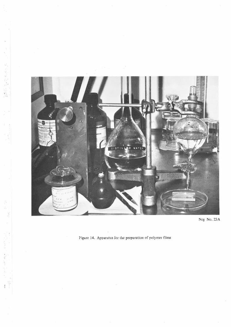
I
, .t
Iij
k
Neg No.23A
Figure 14. Apparatus for the preparation of polymer films

:
73-
by lolvering a glass disc into the polymer solution and withdrawing
at a constant rate, using a small synchronous motor. The with-
drawal rate in this work was 8 cm.min-l. After coating, the disc
is scribed at the edge with a scalpel then placed in a Petri dish,
where it rests against a support at an angle of about 20o to the
horizontal. Distilled water is slowly added to the Petri dish
and the film separates from the disc and floats to the hrater
surface. It is then collected on a 25nn dianeter aluniniun
annulus. Films of turiforn thickness are readily prepared by this
nethod from 2% W/V solutions. When thinner films are required
the glass disc is precoated rvith an evaporated potassium bronide
separating |ayet. The technique is not suitable for the plepara-
tion of thick films because of variation in thickness; however,
a slower wíthdrawal rate may overcone this problem'
All polyrners weÏ.e filtered using Millipore rnicro-syringe
apparatus with MF Mipor or Mitex final filters '
polyner substrates for electron ntic1.oscopy h¡ere prepared by the
above nethod and transferred to grid carriers using a precision
punch. Each 25mm diameter film yielded 6 or more grid carrier
substrates.
5,4.7 Selected polymer filns
The polyner materials discussed above are all easily cast into
thin filns and have useful applications as substrates oI' as
protective layers in vacuum and optical technology. Many other
polyners were investigated; however, these were either difficult
to cast or were inferior to the naterials previously described.
The author is continuing a study of certain pronising high-working-
temperature polymers. Polyacrylonitrile (PAN) in particular, has

'74-
very considerable potential. PAN films have been successfully
plepared by spin coating techniques, but a routine high-yield
process schedule has not, as yet, been perfected for ouf infrared
absorber studies.
In this project collodian and PVC were used for infrared and
thernal studies; collodion, PVC and formvar for electron nicro-
scopy. saran filns have so far proved disappointing; they appear
to rupture easily during deposition and cannot withstand heating
above 70oC. Some relevant properties of the selected polyrners
are listed in Table 3.
TABLE 3
SELECTED POLYMER FILIVIS
RuptureSolvent
Amyl acetate
Chloroforn
MEK/toluene
160
L20
140
MIBK 110
MEK/MIBK 70
2
2
3
2
2
Collodion
Fornvar
PVC
Genclor-S
Saran F-300
Filn TypeConcentration(% Weight Per
volurne)
remleratureoC)
The rupture temperature cited in the tal¡le refers to 25nn
dianeter filns.
It is clearly difficult to predict with certainty tl're suitability
of the various polyners as thin film substrates. Thus we have the
surprising result that collodion fitns will withstand heat treatment
up to 150oC, w¡ereas the other plastics, notably Saran, rupture at
a lower tenpeïatue. The situation is further cornplicated by the
tendency of large-diameter filns to Iuptur.e during deposition' Here
-75
again, collodion proved to be superior to the other naterials
tested. On the other hand, collodion is rnore easily damaged
in the electron microscoPe.
The thickness of colloclion and formvar films used in this
project was 500 to 1200R. PVC was selected when thicker films were
required. These PVC filns were nore uniform in thickness than
collodion (because of the lower vapour pressure of the solvent)
and were free of strong absorption peaks in the infrared.
5"5 Cleaning and handling of substrates
The need for substrate cleanliness in thin filn technology ca¡not be
over-emphasised. In this project direct handling of substrates was
avoided if possible, and where unavoidable, polythene or terylene gloves
were used. In general,however, substrates were cleaned and transported
in glass holders and were manipulated with suitably shaped tweezers.
They were stored ín dust free containers (in some instances vacuun
desiccators), and preparation for deposition was carried out in a laminar
flow work station.
The cleaning schedule used for glass substrates is as follows :
(a) ultrasonic agitation in trichloroethane (Dowclene WR)
(b) clean in hot R.B.S.25 solution
(c) rinse in hot distilled water
(d) rinse in ethanol
(e) rinse in distilled de-ionized rvater
(f) water removal with blast of filtered dry nitrogen
(g) dry in oven at 60 to 80oC in covered container
It witl be noted that the schedule does not include a final solvent
degreasing, e.g.r vapour degreasing in isopropyl alcohol. The solvent
nust be extrenely clean, otheruise a residue will remain on the glass
-76-
surface. The above schedule avoicls this difficulty ancl yiclcls contanina-
tion free substrate!.
Dowclene WR solvent was preferred for the final stage of large scale
cleaning operations.
5.6 Deposition of gold films
All gold filns hrere prepared in the a¡rcilliary coating unit. Gold was
evaporated frorn a 0.25mn thick molybdenum dinpled-strip vapour source.
The evapotant was 0.5nm diameter high purity gold wire.
The substrate arrangement used in the ancilliary coating unit was
sinilar to that described in Section 5.3. A sirnplified resistance
measurement technique was adopted, in which the substrate was inserted
in a sinple voltage divider circuit and the voltage drop monitored witl'r a
d.c. null voltneter. During some depositions filrn resistance and thick-
ness monitor frequency shift were recorded on a Honeywell ultraviolet
spot- galvanoneter recorder.
5,7 Deposition of chromiun filurs
A brief study was rnade of chromiun films for comparison with nickel
and nichrone films. Chromium was evaporated fron a resistance heated
molybdenurn source sinilar to that used for gold. The evaporant was 325
mesh 99.9% pure chromium powder. Chronium sublimes direct fron the
solid and does not alloy with the source naterial. It adheres strongly
to glass substrates, and for this reason is often used as a "keyingrr
layer for poorly adherent evaporants such as go1d.
Chronium films of resistarce 200 ohm per square were found to be very
much thicker than nickel, gold and nichrome filns of sirnilar resistance.
This phenonenon is probably the result of superficial oxidation during
deposition at a pressure of 10-5 torr. Chroniun filns did not show any
marked instability in air; however, the results of this limited study
_77_
are inconclusive, the value of the chromiun depositions lying nainly
in the interpretation of filn structure (Section 10).
5.8 Deposition of nichrone filns
The nickel-chromium alloy used in this project was Nichrorne-V,
nanufactured by British Driver-Halris Co. Ltd. Ttre composition of the
alloy is 80 parts nickel and 20 parts chroniun. The nichrone was
evaporated fron a 3-strand (3 x lmm dianeter) resistance-heated tungsten
wire helix filanent vapour source. The evaporant comprised short lengths
of lnn diameter nichro¡ne wire crimped to the filament. A filanent current
of about 604 at 8.5V was required for deposition.
The filanent was rrflashrr cleaned prior to nelting the evaporant. The
evaporant readily wets the tungsten. However, rapid alloying occurs;
hence to avoid f,ilanent failure a new filament was used for each deposition.
This procedt¡re also helps to ensure a u¡riforn film conposition, as
successive evaporations fron the sane filanent yield a varying nickel-
chronium alloy ratio. The evaporant charge uras approxinately 0.75g.
Filns were prepared in the vacuum coating unit described in Section 5.1
and deposition was nonitored with the apparatus described in Section 5.2.
5.9 Deposition of nickel filns
Nickel filns were studied extensively during this project. Because of
the large number of specinens required for optical, structure and thermal
analysis, two vacuun coating units were used for filn preparations.
Systenatic research studies were camied out using the coating tutit
described in Section 5.1. The ancillary trnit was used for pilot deposi-
tions and certain specialised experinents. This duplication afforded
information on the influence of different nethods of deposition on fil¡n
properties.
5.9.1
s.9.2
-78-Filanent vapour source deposition
A resistance heatecl turtgsten wire helix vapour source was used
for nickel depositions in the ancilliary vacuum coating unit. A
heavy 3-strand (5 x 1run dianeter) helix was employed to avoid
rapid filament burnout due to alloying action, and the weight of
evaporant was kept below t/6 of that of the tungsten source.
The evaporant was Johnson-Matthey Grade A (99.5%) nickel wire,
conmonly ca1led Nickel 200. A filament current of 804 at 3.0V
was required for deposition.
Electron bean deposition
Electron beam deposition was chosen for detailed research
studies on nickel infrared absorber filns. This method of
deposition offers many advantages in thin filn research, notably
the ability to pïepare high purity filns of a wide range of
rdifficultr evaporants. I'lickel is one such difficult naterial.
With the exception of aluminiun oxide, it alloys or reacts with all
conmon source materials. This problem can be avoided with electron
bean deposition. lVhen the evaporant is vaporized fron a water-
cooled hearth or crucible, interaction witlr the source does not
take p14ce. Furthermore, during initial outgassing cycles nany
contaminants are eithe¡ removed from the evaporant by
vaporization, or are "leached out'r to the cold atea adjacent to the
hearth. There is no contamination fron the source natérial and
evaporation takes place fron an intense heat zone defined by the
focussed electron beam. The deposited filns, using high purity
evaporant, are therefore of high purity. In addition, a number of
depositions can be carried out from the same evaporant charge.
A Planer type EBS1 electron bean evaporation source was used for
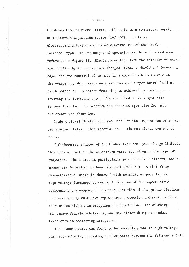
-79-
the deposition of nickel filns. This unit is a commercial version
of the Unvala deposition source (ref. 37). It is an
electrostatically-focussed diode electron gun of the rrwork-
focussedl type. The principle of operation may be understood upon
reference to figure 15. Electrons emitted from the circular filanent
are repelled by the negatively charged filanent shield and focussing
cage, and are constrained to move in a curveci path to impinge on
the evapo¡ant, which rests on a watçr-cooled copper heartl-r held at
earth potential. Electron focussing is achieved by raising or
lorvering the focussing cage. The specified minimum spot size
is less than 1mm; in practice the observed spot size for netal
evaporants blas about 2nn.
Grade A nickel (Nickel 200) was used for the preparation of infra-
red absorber fi1ms. This material has a rninirnum nickel content of
99 . s%.
Work-focussed sources of the Planer type are space charge limited.
This sets a lirnit to the cleposition rate, depending on the type of
evapolant. The source is particularly prone to field effects, and a
pseudo-triode action has been observed (ref. 38). A disturbing
characteïistic, which is observed with metallic evaporants, is
high voltage discharge caused by ionization of the vapour cloud
surtounding the evaporant. To cope with this discirarge the electron
gun pol,{er supply must have anple surge plotection and must continue
to function l,\rithout interrupting the deposition. TIie discharge
nay danage fragile substrates, and may either damage or induce
transients in monitoring circuitry.
The Plane3 soulce was found to be rnarkedly prone to high voltage
discharge effects, including cold enission between the filarnent shield
Neg. No.6A
(a) Planer source with electron deflector plates
(b) Showing focussing cage removed
Figure 15. Electron beam deposition source
Neg. No. l7A

80-
and hearth pedestal. It was found necessaly to make extensive
nodifications to the corunercial power supply, prinarily the
provision of a new RLC filter for suïge linitation, and improved
overload protection devices. A matched Planer power supply tvas
not available.
A marked inprovement in tlre operation of the Planer source was
achieved by inserting an insulator sleeve between the hearth
pedestal and filanent shield of the electron gun. This eliminated
cold enission and reduced discharges during deposition. The
exposed surface of the insulator (see figure 15) became coated
with metal during deposition - although not in direct line with
the evaporant - necessitating cleaníng after each Plocess. Failure
to remove this coating resulted in an increase in the nunber of
discharges, and excessive current leakage. A silica sleeve rvas
found to be the most effective; however, the metal coating was
difficult to ïemove. Boron nitride was subsequently used in the
Planer source. This material is reaclily machined and the metal
contanninant easily re¡noved with a scalpel blade
Another serious characteristic was the high electron density in
the undisturbe<l vapour beam. Tl-ris phenornena is conmon to all types
of high voltage electron beam deposition sources, and is probably
caused by specular ïeflection Of sone of the electrons in the
prinary beam. with the Planer source, operateð at a voltage of
4kV and emission culrent of 100rnA, an electron current of 250p4
was measured at a 25nn dianeter collector plate situated in the
substTate plane. This resulted in total destruction of polyner
menbrane substrates (approxinately 50% of electrons of 4kV enelgy
are absorbed by a 1000R thick polyner film), Ðd it became
-81
inpracticable to monitor film resistance during deposition. This
difficulty was largely eliminated by placing parallel electrostatic
deflector plates above the source, with one deflector held at
filarnent potential. A circular ¡netal plate with a 2cm dianeter
aperture was inserted irunediately above the focussing cage, and was
also held at filanent potential. This amangement is illustrated
in figure 15. The measured electron current at tl're substrate was
reduced to less than 1 uA.
lVe should note, finally, a further consequence of the use of a
water-cooled hearth. Nickel depositions carried out from a graphite
hearth placed in physical contact with the water cooled hearth
pedestal, I^/ere acconpanied by excessive spitting of the evaporant.
No spitting was observed when nickel rvas evaporated from the copper
hearth, which was soldered to the pedestal to achieve maximum
heat sinking.
Nickel depositions fron the copper heartìr were carried out at a
voltage of 4 to SkV and an emission current of 100m4. The filament
current was 18 to 204. Sufficient specimens were obtained to satisfy
the requirenents of this project.
6. OPTICAL MEASUREMENT TECIINIQUES
6.1 Measurement of filn thickness
The thickness of metal absorber filns and polyner substrates was measur-
ed with a Tolansky multiple beam interferorneter. This instrument,
illustrated in figure 16, was designed and constructed in the authorrs
laboratory. The initial design study was carried out by a co-worker
and is described in an internal report (ref. 39). The interferorneter was
alsenbled, aligned and tested by the author and his technical staff. The
author is also responsible for the provision of reference optical flats
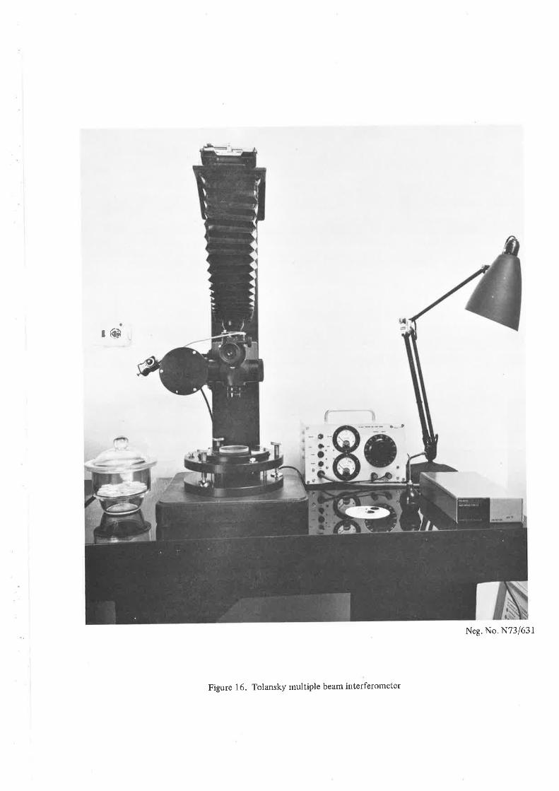
t@
É** -"- ìL'
Neg. No. N73/631
Figure 16. Tolansky multiple beam interferometer

82-
and validation of the interferometer for the accurate measurement of film
thickness.
6.1.1 Tolansky interferoneter
l,lultiple beam interferometry was developed as a thickness
measurement tecl'rnique by Tolansl<y (ref . 40) alld is now well
establisþed in thin filn tecl'rnology (refs. 35, 36). An excellent
review is given in reference 41. ülhen operated in the reflection
node, the technique requires that the thin filn to be measured be
coated with an opaque, highly reflecting surface layer. This layer
is brought into close proximity to a master optical f1at, forming
a narïow wedge between the two surfaçes. The rnaster flat is coated
with a highly reflecting, partially transrnitting surface fi1¡n. This
arrangement is illuminated witlr nonochronatic radiation and the
resultant intense fringe pattern is viewed in reflected 1ight. If
a ledge is formed in the spccilrcn prior to deposition of the
reflecting layer, then the fringe pattern is displaced along the
ledge. The displacement is a lneasure of filln thickness, according
to the equation
r= (n+a/fi| (102)
where n is the fringe orcler, a is the fringe displacement (neasured
as a fraction of one fringe width), b is the fringe separation and
À is the wavelength of the radiation source.
The preparation of the specinen film for thickness measurement is
a simple procedure. The specinen is coated with an opaque silver
layer by vacuun deposition. This layer should be evaporated at
roon tenperature using a l'righ deposition rate to achieve a fine
grain filn. Scrupulous cleanliness is essential. The ledge is
formed on the specinen filn (prio1 to silvering) by etching, or by
-85-
nasl(ing during the deposition. In this project the 25mm diameter
glass substrates described in Section 5.3.3 were used, and the
silvered specimens were stored in a vacuumclesiccatorto avoid
tarnishing.
The ¡naster flat must satisfy certain optical require¡nents if
sharp, high contrast fringes are to be obtained. The fringe
intensity at normal incidence is given by the Airy formula
I (103)f=+Fs n 2n
^where d is the wedge spacing and À the wavelength of incident
radiation.
F is the Fabry coefficient of fineness, and is determined from
.-4RF = fi;z (104)
where R is the reflectance of the coatecl surface of the master
optical flat. Clearly R should be as large as possible. Of more
direct practical value is the fringe half width, l/, which, when
I = Io/2, is given by
w=1*' (105)" rRYz
expressed as a fraction of the fringe spacing. For maximum
resolution we seek a high reflectance.
If the master flat coating is absorbing, the fringe shape renains
the sa¡ne but the contrast is reduced. In the ideal case (no
absorption)
(1 - (1*n) 2co=iäþ , (106)
however, for non-zero absorption the actual contrast is
^c^ = cç/ (1*+) 2 Qo7)
Thus a second requirenent is that the ratio of the absorption to
trans¡nission, A/T, must be as srnall as possible. The fil¡n must,
-84-
of course, be partially transnitting to enable the fringes to
be seen.
The best netallic reflector is silver. llolvever, the highest
attainable reflectivi,t.y for silver films is about 0.95 and the
absorptivity is then approxinately 0.04. I'ltrltilayer dielectric
coatings can be prepared with an absorptiotr of less than 0.005.
These coatings are mechanically durable ancl clo not tarnish, and
hence are an obvious choice for interferometry. Ttre author employed
two rnaster optical flats in this project. 'l-ire reflecting surfaces
were Jacka mirror coatings, one having a reflectance of 0.92 for
routine measurenents, the other 0.95 for high resolution measure-
nents. Assuming A = 0.005, the above theory provides :
I,IASTER 1 R = 0.92 ^/'1
= 0.067 Ca/Co = 0.88 ll = 72.5 R
MASTER 2 R = 0.95 A/T = 0.11 Ca/Co = 0.81 lV = 44.5 R
The line half width is given for a wavelength of 5461R (nercury
green). The reflectances of the mirror coatilìgs l^/ere peaked at
this rvavelength.
The surface of the optical flat should be very smooth; in fact
this is more important than flatness . 'l'he thickness of the flat
should be no less than L/6 the diametcr to avoid flexure and
consequent fringe bending. Finally, it shoul<l l;e thernally stable.
The flats used in this work were manufacturecl from llomosil (silica)
in the Weapons Researçh Estal''lishment optical 1¡rboratories. They
were polished to 1/10 fringes and specified scratch and sleek free.
The di¡nensions of the flats ate 7.Scn dia¡neter, 1.25cm thiclt.
The incident radiation is collinated mercury green light
(wavelength 5461R). The source is a rneoiun pressure mercuïy arc
latnp.

85
6.7.2 Thickness neasurentents
The best fringes are obtained at the snallcst wedge angle and
minimum wedge spacing. The wedge angle is linrited in practice by
localized pressure effects, which cause fringe bending. The
technique used in this study was to set visually the interfero-
meter for the sharpest, undisturbed fringe pattern, then photograph
the pattern with the Polaroid canera attachment shown in figure 16.
The fringe separation anql step clisplacenent rvercr then neasured with
a travelling microscope and the thickness calculated from equation
(102). The final thickness was deduced frorn the statistical average
of a nininum of 6 sample nleasurements.
A typical fringe pattem is illustrated in figure 17. The
measured instrument accuracy using the statistical sampling tech-
nique "", l SR tor films of thickness greater than 100R. It rvas
found that approximately 4 fringes/crn gave the highest accuracy.
The attainable fringe half width was less than 50R, using a master
flat with 0.92 reflectance. The line wiclth set a lower limit to
routine thickness measurement of 50R with alÌ accuïacy of 1 fOR.
With care, gleater accuracy is llossible.
6.2 lt{easurement of spectral absorptance
6.2.7 Infrared spectrophotometer
The transmittance and rcflectance of thin metallic absorber
filns hlere neasured over the spectral range 1 to 16 pm with a
Becknan Mode1 IR4 double-beam infrared spectrophotometer. The
film absorptance was deduced from equation (51). Specimens were
prepared by deposition of the metal on to thin polyrner substTates
mounted on standard 25mn o.d., 20nm i.d. aluniniun annuli, as
described in Section 5.3.4. The thickness and sheet resistance
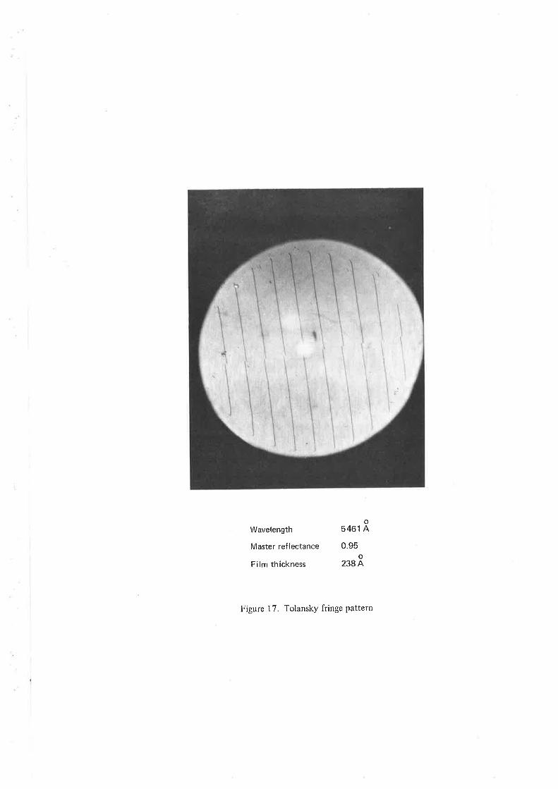
Wavelength
Master reflectance
Film thickness
o5461 A
0.95o
238 A
Figure 17. Tolansky fringe pattern
-86-
of tl're films were determinecl prior to o¡ltical measurement.
The infrared spectrophotometer is illustrated in figure L8.
The Model IR4 spectrophotoneter is essentially a transmission
measuring instrument. Precision work holders have been manufactured
specifically for use with the 2Smm annuli. Spectral transmission
scans ATe executed autonatically over the rallSe l- to L6 ¡rm with a
routine resolution of better than 0.03 um. The transnission measure-
nent accuracy is typically t% or less.
Spectral reflectance is measured with a "reflectance attachmentrr,
rvlrich is provided as an instrurnent accessory. This device comprises
an alurninízed !20o icoscclc.:; ltristn, ancl a spccineu holder. ìlhen
placed in the translnission path, racliation is reflected at a 600
angle of incidence fron the first prisn surface to the specimen
which is orientated paralle1 to the tralsmission path, thence to
the second prisn surface where it is reflected back along the
original path. The radiation path is thus arranged synnetricaLLy,
so that the incident arìgle at the specinen is 30o. Great care
must be taken with aligrlment.
The first step in the reflectance nìeasurement is to insert a
freshly aluninized rnirror in tl're specirnen holcler and execute a
spectral scan. This provides a L00% reflectance reference. The
nirror is then replaced rvith the specimen and a second scan is
calried out. During this entire operation a second r.eflectance
attaclrnent, with an aluminized nirror inserted in its sarnple
holder, is positioned in the reference path of the spectrophoto-
meter to compensate for instrunent spectral non-linearity. If,
at any given wavelength, the reflectance measurement for the
mit='or refelence Scan is gr, alrd for the specinen scan is ps, then
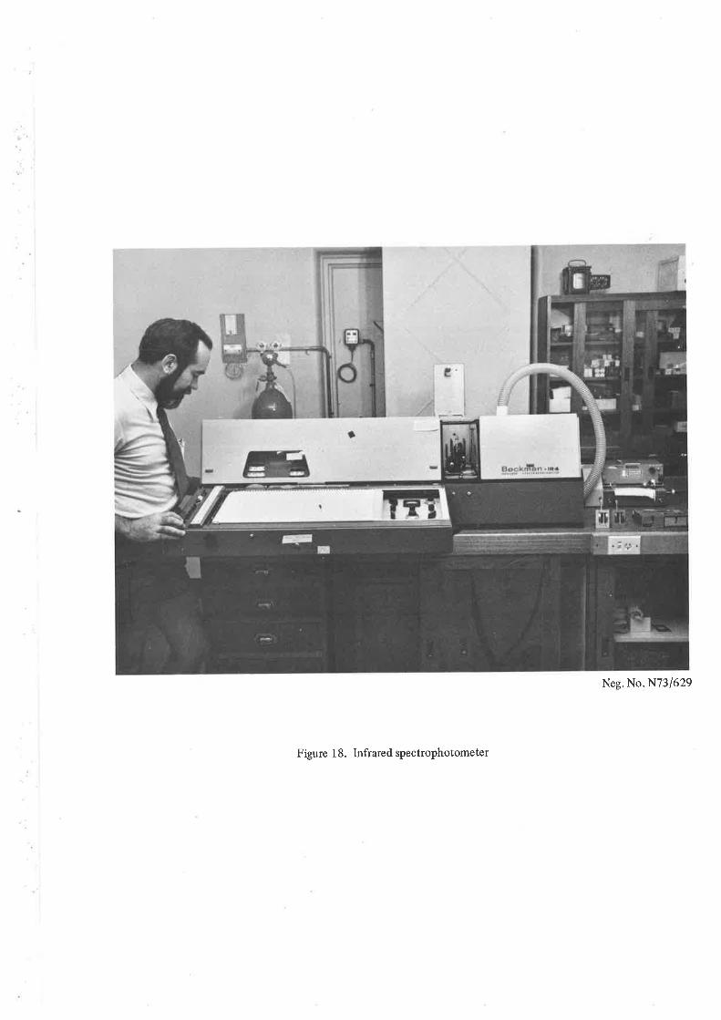
Neg. No. N731629
Figure 1 8. Infrared spectrophotometer
87-
Pr=9p 2
2
pm
andÞs=P (108)
p 0¡
where gn, 9,n and 9¡ are the reflectance of the prism, reference
rnirror and specinen filn, respectively. Ilence
( loe)
Thus the measurelnent of specimen reflectance is independent of the
plisn reflectance but assunes a knowledge of the reflectance of
the aluninized reference rnirror. Fortunatery, this infornation is
well known (see, e. g. , ref . 42) . Furtherntorcr, thc re flectance
of vacuum deposited aluniniurn in the infrare<l is relatively
insensitive to the conditions of preparation. A slrall drop in
reflectance is observed with aging. Consequently, reference
mirrors used in this project were stored in a vacuum clesiccator.
Polyner substrates
In section 5.4.7 a brief sunnary was given of researcrr on polyner
membrane substrates. It was found that of the many polymers success-
fully cast as thin self-supporting filnrs, norìe proved to be superior
to cellulose nitrate (collodion) for use as an infrared absorber
substrate. only one polyner studied, polyacrylonitrile, shows more
pronise; however, we have not yet established a hj-gh-yie1d
preparation technique for ultra-thin films of this material.
Accordingly, collodion substrate filns were used for routine infra-
red measu¡enents. PVC filns were ernployed when a thicker substrate
was required, e.g., when the fragile collodion films were danaged
during deposition, and then only because the pVC substrates have
no strong absorption peaks.
Pç=&-'r
pn
6.2.2
6.2.3
88-'fhe measured spectral absorptance of a 850R thick collodion
filn, at nornal incidence, is shotvn in figure 19. This spectrun is
typical of the substrates used for infrared rneasurenents. There
are four distinct absorption peaks, at 6 ¡rnì, 7.8 pm, 9.5 un and
11.9 um. The spectral reflectanco' is alnlosl constant at
approximately 29o; and the observed transntj ssion spectrun is of
sinilar (but inverted) shape to that sholn in the figure. The
absorption peaks, whilst of minor annoyaJìcc jn absorber measurements,
are used to advantage as a film reference. lle have calibrated the
7.8 ut peak for the measurement of collodion thickness.
The collodion substrate is seen to have relatively J.ittle
effect on the optical properties of nret.allic absorber filns,
particularly for wide-bancl applications. The integrated absorption
over 2 to 16 pm of thc 850R Lhick filnr j-s 0.0C19, arcl over the 8 to
14 um atmospheric window 0.014.
Spectral measurcments
There are two inportant factors rvhi ch nltst bc taken into
consideration in the neasurement of spectral aclsorptance of metal
filns on polymer film substrates, using the instrumentation
described in Section 6.2.1 above :
(a) The influence of the polyrner substrate
(b) The effect of measurement at non-normal incidence
These factors have relevance in both the rneasurement technique
adopted and the interpreÇatjon of the final spectral scans.
Firstly we note that tlie netal film and polyner substrate are
not independent of each other, but in fact together constitute a
composite thin film interference filter (see Section 3.4.2). Thus
the conmonly applied technique of inserting an identical substrate

o.2
0.15
0.1
0.05
62 4 IWavelength (¡rm)
10 12 14 16
Figure 19. Spectral absorption of collodion substrates

-89-
in the reference patl'r of the specttophotonto'tcl , to conlpensate for
the specimen substrate, is strictly invalid. The author has
observed that when this approach is ttsecl tlte spectral characteristics
of the substrate are still reproduced on the spectrophotometer
trace. It is therefore moïe desirable to work with an air reference
and deternine, on alalytical grounds, the colìtribution of the
substrate to the measured reflectance. The simplest apploach,
noting that the polymer film does not greatly influence the final
result, is to ingore the substrate altogether. In practice it is
usually the substrate-absorber conbinat,Lol't rvhich is of interest.
In this project results are quoted for the composite film and
substrate thickness ís recorded as a Paranìeter'
The second factor concerns the angle of incidence used in the
spectrophotometer measurements. lVe have'regularly observed in
absorber studies that the measured reflectance of the cörnposite
film varies by up to 5%, depending on whether the netal absorber
(which we call side cr) or the polyrner substrate (side ß) faces the
incident bearn. 'fhe reflectanÇe of sicle c is always higher' The
explanation lies in the theory stated in Section 3.4. The
difference in reflectatìce ca¡ìnot be explained in telns of the
theory for nornal incidence. This tl-reory states that the
transnittance should be the same for sides cx, and B, and this is
in fact observed. Ìlquations (76) and (78) predict that the
reflectance fo1 side cx is higher than that for side ß, but for a
1000R thick polymer substrate the diffelence is insignificant.
However, for a 50o angle of incidence, the reflectance of the
absorber alone is expected (equation (74)) to be 3.7e" higheT than
at normal incidence, for a 189 ohn per square film. We therefore
-90
deduce that the observed difference in reflectalrces for sides o
and ß is assocj.ated with the large angle of inciclence.
Ïre solution to this problem is elucidated in figure B. The
transmittance is sinilarly influenced by angle of incidence, but
the resultant of absorptance is alrnost inclependent of measurement
angle. lletrce jt is ilryrortant that thc reflectance and transmitta¡ce
are both measurccl for the same side of the composite absorber
filn and at the sane angle of incidence. l{hichever side is neastrred,
the resulta-¡rt absorptance - deternined from equation (51) - should
be the sanle, and very nearly equal to the value at normal incidence.
This is indeed what is observecl in practice.
6.3 Measurenent of total emissivity
6.3,I Emissivity apparatus
An alternative ntethod of cleternining the absorptance of a thin
infrared absorber film is to measure the radiant emittance (radiant
power per unit area), lv, of the specimen filn, and then conpare
this value with tlte radiant emittance, lVO, , of a blackbocly at the
same absolute temperature. Frorn the Stefalr-Boltzmann Larv
e = lvlwou (110)
where e is the emissivity (strictly, emissance) of the specimen,
and is equal to the absorptance (see Section 3.1.). This value of
e ís the total enissivity, i.e., integrated over the blackbody
spectrum for the given ternperature. IJowever, if, as theory predicts,
the absorptance spectrum is flat above 2 ¡-rm wavelength, then the
total greybody absorptance should compare favourably with the
spectral absorptance measured as described in the preceding
subsection.
- 91 -
The emissivity of absorber filnrs was tneasru'ed lvith an
Emissivity Test Apparatus, which was designecl and assenlbled by
one of the authorrs associates. The authol' is .responsible for
recent modifications, introduced to inrprove instrulnent sensitivity.
The apparatus consists of an isothermal enclosure and a broad-band
infrared radiometer. The specimelr to be measurcd, usually in the
fonn of the standard 25mm diameter annulus, ì.s placed in the
enclosure adjacent to a blackbody reference of roughly the same
dimensions. The specimen and blackbody are ntounted on a rotatable
disc (the "specinen wheelrr), which is rnachinecl to accommodate a
nrunber of additional specimens for analysis cluring the same
measurement cycle. The wall of tl-re enclosure is water cooled and
the charnber itself is heated with a controlled warm air draught.
A potassiunr bromide window is fitted to the wall of the enclosure
for specimen observation.
The specimen ancl windolv are situated on the optical axis of the
infrared radiometer. The racliometer comprises an f/0.8, 25mm
focal length nonocentric reflecting optical system, and a germanium-
irunersed therrnister flake bolometer detector. The radiation is
rnechanically chopped at a frequency of 72Ilz. An optical rnodulation
reference signal is provided by a pea-lamp-photodiode combination
fitted to ti're chopper wheel assembly.
A new low noise amplifier, rvith phase sensitive rectification, is
being developed for the Enissivity Apparatus. In this project, as
a tenporary arrangement, tÌte author used a P.A.R. Model HR-8
precision lock-in amplifier to process the detector output. The
anplifier was phase-locked on to the chopper reference and the
amplified output signal was monitored on a Minigor Type RE501
-92-
potentiometric chart recorder.
The Emissivity Test Apparatus is illustrated in figure 20. The
radiometer cover hras removed for the photograph to clisplay the
optical system, and the lid of the enclosure is shown raised to
illustrate the specimen holtlcr arrangenìent.
During operation, one of thc specimen holders is left blank,
exposing a clear aperture on the spccimen wheel. When the disc is
rotated the detector fielcl of view images, in turn, the specinen,
the blackbody referencer ûncl thc wall of the enclosure. It is
essential that the wall of tllc c-'nclosure l¡e at constant temperature;
otherwise the measu::ecl absorlttance will be in error, the error
being a maximunr for L00i; rcfl,ccting fihns. Iror this reason an
aluminized nirror was included in one of the specimen holders, to
act as a zeto absorptance refercnce. T'he specinen wheel is slightly
rotated from the normal to avoid 1¡ack reflection to the detector.
This procedure leads to a rem¡rrl<ably sinple conrputation of specinen
enissivitlr âs derived in the folJowing analysis.
If the tenperature of tlrc 5psginen ancl tire blackbody is f (of)
and the ternperature of the enclosure wall is T'o (oX), then the
radiant emittance, as lneasuled at the detector, is :
for the blackbody,
\o = oT4 (111)
for the enclosure wall,
l1/o - oTo4 (rLz)
and for the sample,
lll = 6s14*poTo4*.oTo4 (11s)
where e, p and r are the emissivity, refrectance and transrnittance
of the sanple. Noting that
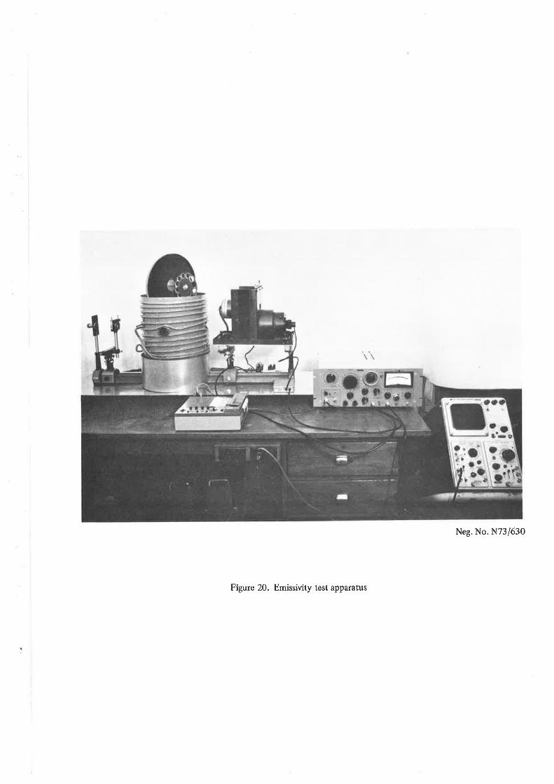
Neg. No. N73/630
Figure 20. Emissivity test apparatus
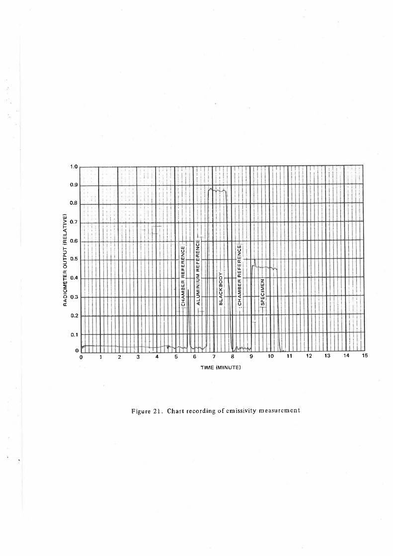
1.0
0.9
0.8
l¡J> 0.7F-
J
Ë o'ut-lÈ o.sloEH o.¿UJ
=9o o.3É.
o.2
o.t
0012345678
TIME (MINUTEI
9101112131415
Figure 2l . Chart recording of emissivity measurement
-
II
I
I
tI
zt¡l
õluLØ
t¡l(,zl¡JÉt¡JlrUJGtrt¡Jo
Io
ooovoJ6
t¡Jozultrt¡¡t¡-uJtrã2
=fJ
uJozl¡,úulttI!
trt¡Jdl
¡o
I
I
I
I
I
I I
¡
1
i
I
I
I
I
I
i
I
I
irlitiiii
I
1
-93-
e+p+r - 1,
a sinple reduction gives
W-Wn
' = w';;wo (114)
Thus if the detector amplifier is linear, then the filnenissivity can be calculated from
^ - V-Vo' - Fvo (11s)
where V, Vo and V55 are tlte cor:resporÌding signal voltages. TLe
technique therefore requi.r'es rneasurctnent only of relative signal
voltages,
The procedure describecl above was f'ollowecl in this project. A
typical output trace is sholn jn figr.rre 21,
7. GOLD FITMS
Gold filn infrared absorbers ancl bolomcter detector:s have been used
extensively in the authorrs laboratory. Experinental techniques for the
preparation of gold absorber films have been established for rnany years, and
nunerous measurernents have been made of ínfrared absorptance. Nevertheless,
gold was studied in this project for two reasons :
(a) Gold is known to fern coarsely crystalline, aggregated deposits. rt is
desirable to study a material of tl-ris type in order to test, and hopefully
validate, the theory and predictiorìs enunciated in earlier sections of
the thesis.
(b) We have not ful1y understood many of the observed physical properties of
of gold absorber filns. 'lhe preserìt study, with its broad research basis,
should help to clarify previous areas of doubt.
7.I Film deposition
A total of 25 gold films lùere prepared in the ancilliary vacuum coating
unit. The deposition rate, with one exception, was 1.0 to z.oR.s-l. The
_94_
exception was a single deposition at 0.fR.r-l, carried out to assess the
influencc of a slow rate on physical properties.
Thickness was measured for eight specinens. The quartz crystal nonitor
calibratíon is shown in fígute 22. Also plotted is the theoretical
prediction determined from equation (994), which is based on the bulk
density of 19.39.cm-3. The rneasured thicknesses suggest an apparent
filn density of 73.79..^-5. An evident error of 20 to 30R for two of the
specinens has been traced to cont¿unination of the optical flats due to
poor cleaning. The actual thickness measurements aïe accurate to i SR.
7.2 Electrical properties of gold films
The nost noticeable electrical characteristic of gold filns deposited
on to glass substrates is that it is difficult to prepare a fiLn of
precisely determined resistance. When deposition is stopped the film
continues to trformrr, with a consequent resistance overshoot; and the
resistance nay continue to fal1 through many orders of magnitude. The
greatest change takes place rvithin a few minutes of deposition. A film
deposited to 200 Q per square will typically stabilize at 50 a per square
or 1ess. Much the same final result is obtained if deposition is stopped
at 500 CI per square. The resistance overshoot is less marked for polymer
substrates. A 200 CI per square filn was observed to stabilíze at 120 a
per square.
The final resistance u¡as found to be sensitive to deposition rate, the
type and condition of the substrate, and the substrate terperature. Thus
the onset of conduction for a filn deposited at 0.fR.s-l vras noted to occur
at roughly twice the thickness of films deposited at 1 to ZR.r-l. Con-
versely, conduction co¡nmenced at a lesser thickness for films deposited at
a high deposition rate.
400
o<6o,È-v,.9EF
E=TL
0 1 000 2000Frequency shift (Hz)
3000 4000
P
,tø'Ë
u,t
Figwe 22. Quartz crystal monitor calibration for gold films
2000
Frequency shift (Hzl
o.2
0.1
0
o
o
o
o
Edwards Modèl 1
resonant frequency 6 MHz
oooo
oo
o
o
oo
o
o
Edwards Model 1
resonant frequency 6MHz
1 000
Figure 23. Emissivity of gold fìlms
3000 4000
95-
Contrary to expectation, conduction was observed to commence at an
earlíer stage during deposition for filns deposited on to collodion
substrates, than for films prepared on glass substrates; and the final
resistance was lower for the collodion substrates. This is .probably
a consequence of both the higher mobitity on the glass surface and the
coarsely crystalline structure of the gold filns. The latter probably
favours coalescence at al earlier stage of growth on the uneven polymer
substrates.
The technique employed by the authorrs associates for the preparation of
gold bolometer elements on collodion substrates provides for the applica-
tion of a d.c. rrforming currentrrduring deposition, generated frorn a
constant curlent pohrer supply. This is followed after deposition by a
rrcurrent aging", in which the applied current is higher than the normal
operating bias current. The optimum forrning conditions are determined by
experinent. For example, the short circuit "forming currentrr for a 0.2nn
long x 0.05mn wide bolometer element was 100 ¡rA, and the applied voltage
was I2Y. The maxinurn power transfer would occur when the bolorneter resis-
tance is equal to the source resistance, which in this case was 120k4.
Thus dgring coalescence 500uW poweï (3Wcm-2 fo, this detector size) at a
voltage of 600Vcn-1 "", applied to the elenent. Presumably Joule heating
would cause a rise in ternperature as isla¡rds coalesce; however, the
average temperature rise would be insufficient to darnage the polymer film.
In this project we have confirmed by experínent that the above technic¡ue
induces conduction in gold filns which would otherwise be highly resistive
or insulating. If the postulate of a temperature rise on a rnicroscopic
scale is indeed correct, then the phenomenon is in agreement with Choprars
work on field-induced coalescence in gold films (Section 4.3.3, ref. 50).
Finally, electrical aging effects, including the resistance overshoot
-96
observed on the conpletion of deposition, is considered to be caused by
recrystallisation. This is borne out by structural studies repotted in
Section 10.3.
7.3 Infrared optical properties of gold filns
The author has found no sinple relationship between the sheet resistance
and infrared absorptance of gold films deposited on to collodion substrates.
However, there is a unique relationship between absorytance and thickness,
which is evidently independent of deposition rate and electrical aging.
Thus the theory of Section 3,4 does not apply to gold films prepared on
amorphous substrates at room temperature. This is not to say that the
theory is incorrect, sinply that it is probably applicable only on a
nicroscopic sca1e. Structural studies (Section 10.3) show the filns to be
iregular and coarsely granulated and, in the region of rnaximum absorptance,
structurally discontinuous. In agreement with theory, maximun absorptance
is 0.5.
Infra¡ed emissivity for several gold specimens, measured with the
Emissivity Test Apparatus, is plotted as a function of filn thickness in
figure 23. Thickness is recorded as frequency shift for the quartz crystal
monitor, because of an anonalous thickness measurement for two specimens.
Reference to figure 22 shows that the rnaximurn enissivity is attained at
a thickness of 160R. The thickness is seen to be critical. To achieve a¡r
emissivity, and hence absorptance, greater than 0.4, a frequency shift of
1500H2 to 1600H2 is required, corresponding to a thickness variation of at
most 20R. In this study the largest measured emissivity (absorptance) was
0.41. There is anple evidence, frorn the work of the writers associates,
that an absorptance approaching 0.5 is possible, and that the maxinun is
achieved at a frequency shift of approxinately 1600H2 with the Edwards
monitor. The results shown in figure 23 are, however, the first showing
_97
a precise thickness dePendence.
Nunerous neasurements of the spectral transrnission and reflectance
of gold films caried out in the authorrs laboratoty have shown that the
absorptance is not spectrally flat in the region 1 to 16 um. The
deviation from spectral lineatíty is least in the region of naxirnun
absorptance, but the absorption increases at the shorter wavelengths for
both thicker and thinner films. The spectral absorptance at 10 pm was
found to be typically 3 to Seo lower than neasurements made with the
Emissivity Test Apparatus. However, when integrated over 8 to 14 Um,
the two nethods of ¡neasurenent were in good agreement'
Upon consideration of the results of the previous subsection it is not
surprising that the sheet resistance of two specimens of identical
a,bsorptance can vary fron 50Q per square to at least 101'lfJ per square.
This result has a particular bearing on the preparation of gold filn
bolometer detectors. For these detectors we usually seek a stable resis-
tance of 50 to 1004 per square. It appears fron this study that the
deposition rate of 15Hz.s-1 (1.2R.r-1¡ ,,otrally selected in the preparation
process, is in fact an optimun value. Deposition at this rate will achieve,
in conjgnction with the electrical forming technique, a filn of both the
desired resistance and optimum absorptance. A faster rate will give films
rvhich are too thin, and the converse applies to slower rates. It follows
that detectors which do not have the correct thickness should be rejected,
albeit that they have the desired electrical characteristics, because the
detector responsiVity (i.e., volt per watt' see ref. 43), is dependent
on infrared absorptance.
8. NICHROME FILMS
8.1 Some reported properties of nichrone filns
Nickel-ctrromiun alloys have been extensively investigated as resistance
-98-
elements in thin filn nicrocircUits. 'lhe preparatiolt ¿ur<l electrical
properties of these films are widely reported (see references 44 to 48) '
Some relevant characteristics of therrnally vaporised 80/20 nickel-chromium
fi lms
(a)
are as follows
Because of the higher evaporation rate of the chromium coÍponent
it is necessary to use a source tenperature in excess of 1600oC to
retain stoichiometry in the deposited film' At lower ternperatures
the filns ate chromium rich.
(b) Nickel-chromium filns oxidise on exposure to the atmosphere and the
filn resistance rises slowly after deposition. The percentage change
in resistance depends on composition and thickness ' Fitms used in
micro-circuitry are usually stabilized by heating the substrates to
at least 250oC during deposition, followed by post bake cycles ' This
acceleïates the aging process. Filns of resistance greater than about
4001ì per square are unstable and cannot be effectively aged'
(c) The thickness of a 200CI peï squaïe filn on a glass substrate is
reported to be 75 to 100R. Ï're thickness of a filrn of the sane
resistance on a plastic substrate is found to be 250 to 300R, and on
an alunina substrate approximately 500R'
The reported structure of nichrome filns is discussed in Section 10.4'
published reports on the preparation of nickel-chromium filns have been
a valuable guide in this project. However, the author is not aware of
any reference in the literature to the infrared a¡rd thermal properties of
these filns, the only known work being that carried out in the authorrs
laboratory.
8.2 Fihn deposition
The deposition technique for nichrome filns is described in Section
5.8. 15 specinens vlere prepared, this being considered a sufficient nunber
-99-
to establish the basic absorber properties of filns of this material.
The Edwards thickness monitor was calibrated over the range 80 to 150R.
It was found that the calibration curve changed slope at a thickness of
approximately 110f,, indicating a change in the density of tl're evaporant.
This is not unexpected in view of the discussion in the previous sub-
section, noting that a new filanent and alloy charge was used for each
deposition. The calibration is shown i-n figure 24. The apparent density
of the nichrone filns, determined frorn equation (994), is 5.1 g..*-3 fot
thicknesses less than 125R. Tre density approaches the bulk value of
-78.41 g.cm " for thicker filns.
Nichrone filns h¡ere pïepared at a deposition rate of 2.5 to O.OR.s-1.
8.3 Electrical properties of nichrome filns
Nfost of the electrical data for nichrome filns was measured on glass
monitor substrates. The dependence of sheet resistance on thickness for
freshly deposited nichrome filns,prepared on glass substrates at room
tenperature, is shown in figure 25. The films becone electricz.lly
conducting between 60 and 70R.
An experiment was carried out to determine resistarce on collodion
substrates. Sheet resistance was nonitored on both glass and collodion.
It was found that the resistance on collodion was 1.2 to 1.4 tines higher
than on glass over the r¿mge 100 to 1000CI per square. This is in agreernent
with rneasurements made on 25mm diameter annuli, using the jig described
in Section 5.5.7. The estimated dependence of resistance on filn thickness
for collodion, deduced from monitor recorder traces, is shown as a
broken line in figure 25. These filns become conducting at a thickness of
approxinately 80 to 90R.
Figure 25 shows that thickness of a 200fì per square nichrome film is
approxinately 120R for glass sribstrates and 140R for collodion substrates.

q(¡)cJ.9!
Ell-
150
r00
0
50
500
400
300
200
100
Eõc'L(¡)o.
E.co0)oco.9(¡,É.
0 100 200 300 400 500
Frequency shift (Hz)
600 700 800 900
Figure 24. Quartz crystal monitor calibration for nichrome films
100
Thickness (angstroml
o
o
o
o
o
oEdwards Model 1
resonant frequency 6MHz
\o\
\o \
\\
\o
oo
oo
O Glass substrate
Collodion substrate
00 50
Figure 25. Resistance of nichrome ñlms
150 200

- 100
The film conductivities are thus 4.2 x 10³ n-1..t-1 "rrd
3.7 x L03 n-1..t-1
respectively. The bulk conductivity of Nichrone-V is 9.1 x 10³ çf1' "*-1.It nay be noted that the conduçtivity for collodion substrates is much
lower than reported in the literature (Section B'1)'
Nichrone filrns can be prepared to an accurately predetermined sheet
resistance. Deposition can be stopped at exactly the desired value, in
narked contrast to the Tesistance overshoot observed for nore nobile
evaporants such as gold. However, the fil.m resistance rises on exposure
to air, the percentage change depending of the value of the initial
resistance of the freshly evaporated film. The resistance of filns of
less than 5ggQ per squaïe tends to stabilize with tine; whereas the
resistance of thinner films continues to rise. The typical percentage
change measr¡red over a period of 2 yeats (glass substrates) was found
to be as follows :
lggfl per square Seo
200A r n 10 to 15%
S00f¿ il rt 259o
10004 r r 409o
The rise in resistance is accelerated by thernal aging'
The resistance of nichrone fil¡ns prepared in a poor vacuum were observed
to be much higher, for a given thickness, than the values shown in figure
25. There is little doubt that this is a consequence of oxidation during
filn formation. The influence of cha¡nber pressure is discussed in Section
9 .3.
8.4 Infrared optical properties of nichrone filns
A total of 8 films u¡ere prepared for infrared absorption measurement '
Unfortunately several of these were damaged prior to the completion of
spectrophotoneter records. Three specinens were selected for detailed
analysis.
101
The most obvious experimental result was the relative ease of prepara-
tion of filns having near-optimun absorptance. Indeed nearly all of the
filrns had an emissivity (absorptance) in excess of 0.4, covering a
resistan'ce ïange of roughly 100 to 350CI per square (measured on collodion
substrates). The naxinum observed absorptance, as measured with botl'r
the spectrophotoneter a¡rd the Emissivity Test Apparatus, was 0.49 to
0.5, The nacinum was obtained for filns deposited to 175 to 200Q per
square on collodion. At the tine of meauurcement the film resistance had
risen to 225 to 2504 per square. The spectral absorptance of all specimens
was flat to within a few percent over the spectral range 2 to 16 Um.
The above results are in good agreenent with the theory of Section 3.4,
whictr predicts maxinum absorption at 1B9A per square, with essentially
no wavelength dependency. Here again we shall find that there is a close
relationship between the observed physical properties and filn structure.
9. NICKEL FILI\4S
Throughout this project major enphasis has been placed on an analysis
of the properties of nickel films. A total of 60 nickel depositions
were carried out. Of these, more than half l^rere prepared by electron bean
deposition. The remainder were deposited from resistance heated tungsten
filaments.
The selection of nickel as an appropriate metal for study was based on
a systematic theoretical analysis of the thernal, structural and infrared
absorption properties of thin metallic filns. 1'{ickel is representative
of the evaporants which, according to our earlier predictions, should
have the preferred absorber characteristics. Its melting point (172soK)
is significantly higher than the ninimun value of 1350of specified in
Section 4.4, and we may therefore be reasonably confident of achieving
the desired filn structure.
-702-
Preli¡ninary experiments with platinum - probably a more suitable absorber
material - have indicated that there are several technical problens to overcome
before proceeding to higher nelting point evaporants. Research on nickel has
served to solve many of these problems, ffid the experinental results have
indicated the direction along whidr future work should proceed.
9.1 Filn deposition
Deposition techniques for nickel filns have already been discussed
(Section 5.9). Both the Toyocom and Edwards thickness nonitors were
calibrated, the former for electron bean deposition and the latter for
tturgsten filament sources, from a total of 27 thickness measurements. The
measured data for electron bean deposition, together with the predicted
monitor calibration (based on equation (998) and the bulk density of
nickel), are shown in figure 26. Fron the linited neasurements for
filament vapour sources, we can say little about the thickness relation-
ship for this nethod of deposition, other than to establish a general
trend. The measurements for electron beam deposition are sufficiently
comprehensive to exhibit a narked scatter in the thickness data. lVe may
again deduce an apparent density fron equation (998), and find here a
range 3.0g..*-3 ao 4.Sg.cfl-3, conpared to the bulk density of 8.9g..*-3.
The thickness neasurenents are accurate; hence we must presume a variation
in the density of the deposits. Sone measured points are onitted in the
figure. These concern depositions which yielded an excessive thickness
for a given frequency shift, and were the first experimental indication
of an franomalousrrdeposition process, to be discussed in Sections 9.2 artd
9.3.
For ttmgsten filarnent source deposition, the estimated film density
was 5.5g.cn-3 ao 6.5g.cr-5. A very fast deposition yielded a density of-7l. ¿g.cm
ø0)cv.gE,l-
o
300
200
100
0 100 200
Figure 26. Quartz crystal monitor calibration for nickel fìlms
300 400 500
Frequency shift (Hz)
600 700 800
qO
?o
go
oo
o oo
oo
o oToyocom Model TVF-lresqnant frequency SMHz
electron beam deposition
-105-
The deposition rate for electron bean deposition was varied from
1.5R.r-1 ao +.OR.s-1; for filament source deposition the rate was r.SR.s-1
to 8. sR. s-1.
A further discussion of film density is given in Section 9.3.
9.2 Electrical properties of nickel filns
The neasr¡red sheet resistance of nickel filns on glass artd collodion
substrates is plotted in figures 27 and 28. At first sight it rvould
appear that the observed resistances are too widely scattered to
establish a firm dependence on filn tl'rickness. Fortunately there is a
plausible explanation for the experimental results. Tl-re data shown in the
figures are representative of uniforn (constant rate) depositions; lower
resistance values can, in general, be traced to a fast deposition rate,
and occasionally to an inproved vacuun. A number of measurenents are not
recorded. These were cases of excessively high resistance, and witirout
exception all such observations could be traced to either a slolv deposition
rate or a slowing of rate during the early stages of deposition. For the
electron bean deposited films a high resistance was often associated with
culrent leakage across the boron nitride insulating sleeve, causing a sharp
drop in deposition rate. Nickel filns so pnepared were semiconducting.
The resistance of nickel films deposited on to collodion substrates was
for,¡nd to be L.2 to 1.5 tines higher than films of the sane thickness on
glass substrates.
9.2.7 Electrical conductivity of nickel filns
Fron figures 27 artd 28 it is found that the thickness of a 200 Q
per square nickel film is 90 to 100R on glass substrates, and 130 to
150R on collodion substrates. These filns are slightly thicker
than nichrone filns of the sarne resistance. Ilowever, the electrical
conductivity is approxinately 5, x 103 fì-1. cm-1 for glass substrates

200
300
100
300
200
100
o<Ø(¡,trv.9Et-
500 100
Resistance (ohms per squarel
Figure 27. Resistance of nickel films on glass substrates
100 200 300
Resistance (ohms per square)
150
400
200
Øo)c
.v,
.9El-
o
0
o oa
oao
oa oo
ao
aoo
oa
O Electron beam deposition
6 Tungsten filament deposition
oaa
oa
o
a
OO
O Electron beam deposition
I Tungsten filament deposition
Figure 28. Resistance of nickel films on collodion substrates
500

L04 -
3 -1 -1.cmarid 3.5 x 10 CI for collodion substrates¡ compared to the
bulk conductivity of 1.1 x 10⁵ s¿-l.crn-l. It is of interest to
comp¿rre this result with theoretical predictions.
In Section 3.5 we deduced a mean free path for conduction
electrons, based on one free electron per atom, of 65R. The
assumption of one free electron per atom is questionable, because
there is evidence (ref. 49) that only the 4s-band electrons in
nicl<el contribute to conduction, there being approximately 0.6
conduction electrons per atpm. Applying this correction to equation
(89) we obtain a mean free path of 93R. The Fuchs-Sondhiemer theory
(see figure 9) provides that the ratio of bulk conductivity to filn
conductivity, o Jo, for a diffuse scattering rnechanisn is
oo/o =1.45, t=100R;
consequently the resistance should be 14fì per square. We have seen
that this is not the case for the films prepared in this study. For
a looR rhick fitm,
ao/o > L5 for glass substrates, and
oo/o > 20 for collodion substrates.
Clearly the Fuchs-Sondhiener theory fails for these filns. 1'his can
be attributed to :
(a) filn density much lower than bulk density,
(b) high concentration of scattering centres, e.g., adsorbed gases,
(c) low film purity
l'lith regard to (a), the apparent film density (Section 9.1) gives
a nean free path of 147R. This only partially explains the low
observed fil¡n conductivity. In Section 9.3 we will present arguments
in support of conclusions (b) and (c).

-10s-9.2.2 Electrical aging
The resistance of nickel filns always dropped stightly in vacuo
following deposition, typically stabilizing at approximately 95
to 9Be¿ of the freshly deposited filn. There was no marlted rrovershootrl
such as observed with gold filrns, and it was therefore possible to
prepare filrns of predeternined sheet resistance'
0n exposure to air the resistance of nickel films was observed
to rise imnediatety, thence to stabilize wíthin one hour of air
admission. Thenceforth the resistance rose slowly, the overall
percentage change depending on the value of the freshty deposited
film.
The initial rise in resistance was usually no nore than 5% for
glass substrates, with an overall rise, neasured over a period of
several npnths , of 25% maximum for filns of 100 to 5004 per square.
The initial rise was higher for collodion substrates, a maximurn of
25% beíng recorded for a 5004 per square filn. Over a period of
several nonths, the resistance of thick films rose by at least
259o, wltilst for filns of resistance excceding 5004 per square, tire
rise was in excess of 1-00%'
Absorber films deposited to a sheet resistance exceeding 300CI
per square u¡ere too unstal¡le to be of practical value. IVe shall see
(Section 9.S) that aging does not seriously influence the infrared
optical properties of thicker niclcel filns; certainly over the
expected working life of infrared detectors incorporating these
absorber elements.
9.3 Vacuum and oxidation
We have seen that there are five disturbing factors arising from the
experimental results for nickel films, narnely :
106
(a) the apparent filn density is much lower than the bulk density;
(b) there is considerable scatter in the observed filn resistance,
¡neasured as a ftrnction of film thickness;
(c) the electrical conductivity is very nuch lower than the bulk
conductivity;
(d) there is a relatively large rise in filn resistance on exposure to
air; and
(e) we have evidence ofrrano¡nalousrr depositíons, apparently associated
with low deposition rates, which yield films of a very high resistance
for a given thickness and excessive thickness (low density) for a
given crystal nonitor frequency shift.
Oxidation cannot fully account for the low apparent film density,
because the oxide NiO has a density of 6.679.cn-5. We can,however,
expect the structure of the filrn at least to partially contribute to a
reduced filn density. This rvould seern to be the case for gold films (Sec-
tion 10.3), although nickel filns are more continuous and are finely
crystalline. 0n the other hand, we have evidence that a slow deposition
rate (less than fR.s-1) gives ve¡y low density filns, whereas a high
deposition rate (greater than 10R.r-1¡ yiutds almost bulk density. Could
occluded gas cause a decrease in density?
Possible contributory factors to (b) through (e) are low film density,
excessive electron scattering, occluded gases and low filn purity
(including oxidation) .
It seens likely that the solution to the above problens lies in the
inpingement rates at the substrate of both the evaporant a¡rd residual
g¿rses. The evaporant impingement rate is readily deduced frorn equation
89, thus 2
N, = Nn fi R¿ atorns .r-2.r-1, (116)
t07 -
where as before NO is Avogadrors number, p is the bulk density (g.tt-s),
M is the nolar mass (g.nof-l), Ðd RU is the deposítion rate ¡"rn.r-I¡.
It can be shown (see ref. 35, p. 1-81) that the arrival rate for residual
gases is
Ng = 3 .sr3xl022(ugT)-% p molecule "*-2.,-1 (117)
where Mg is the ¡no]ar mass of the gas (g.mol-t), t is the absolute
temperature lof¡ and p is the partial pressure of the gas (torr).
A recent partial p1essure analysis carried out by associates in the
authorrs laboratory has shown that, for vacuurn coating units sinilar to that
described in Section 5.1, the major gaseous contaminants are water vapour
(nass 18) and a nass-28 constituent (probably carbon nonoxide). This is
essentially in agreenent with the results of other workers in the field.
At 10-6 torr the water vapour partial pressure was 6 x 10⁻⁷ torr, and the
nass-28 conponent 3 x 10⁻⁷ to"r. ltlhen the ctra¡nber pressure increases (e.g.
during outgassing) the two najor conponents increase in roughly the sane
proportion, although water vapour aPPears predoninant.
During our nickel depositions we may expect a water vapoul partial
pressure of 5 x L0-6 to 1 x 10⁻⁵ torr. The arrival rate at the substrate
is then1c, -2 -1Ng = 4 x 10.- nolecule cm -.s -
This rnay be compared with the inpingement rate for nickel atons, tvhich,
for a deposition rate of zR.s-l, is. -1s -2 -1Nr = 2 x 10-- atom cm -.s
This is a far fron satisfactory situation. These conditions would favour
the trapping of gas nolecules during film growth, and deposition takes
place in a highly oxidizing atnosphere. Reference to data on the heat of
oxide formation for nickel (see, €.g., ref. 55, Ch. 2) would suggest that
rreactive evaporationrr takes place, so that nuch of the nickel is oxidized

-108-
during deposition. There is now little doubt that the I'anomalousrl
depositions referred to earlier are associated with film oxidation, md
that the low apparent film dertsity can be traced, in part, to occluded
gas. Adsorbed gas, in addition to the finely crystalline stTucture of the
Ni-NiO filn, would be expected to cause excessive electron scattering,
further decreasing the filn conductivity.
The influence of chamber pressure and deposition rate has been noted
by other authors (refs. 34, 46 and 50). In order to rnininize oxidation
and gas occlusion we need to seek a ratio of nickel atoms to water
vapour molecules of at least 10:1. This requires a deposition rate
exceeding fOR.s-l and a chamber pressure of less than 1 x 1O-6 torr. It
may also be advantageous to deposit a thin dielectric filn (e.g., silicon
nonoxide) on to the nickel absorber to reduce post-evaporative aging
effects. A higher substrate tenìperature is desirable, but unfortunately
st¡bstrate heating is limited by the polyner mernbrane substrate.
It is also of interest to note that the ratio of evaporant atons to
r,¡ater vapotrr molecules for our chromium depositions (Section 5.7) is
about 1:2. In view of the high heat of oxide formation for chronium, it
is not sr:rprising that these filns were muclt thicker for a given sheet
resistance than either nickel or nichrone filns. 0n the other hand, we
nust also expect to find an oxide phase in nichrone filns.
Finally, we should keep in mind that these ionsiderations would also
apply to any other high melting point evaporant which might be considered
to be a potential infrared absorber naterial. 0n these grounds alone, we
can eli¡ninate nany naterials. On the other hand we may single out certain
evaporants, e.9., platinun and palladium, which would appear to show
particular promise as absorber materials.
-109-9.4 Stress in nickel filns
Mcchanical stress in nickel films iurposed a serious technical
limitation, when the films were deposited on to thin collodion substrates.
Stress was observed to cause "burstingrtof the film at a substrate
temperature well below tlÌat of the tested rupture temperature of the
collodion. ltfhen fitns survived deposition, the coate<l sul-rstrate sagged
on exposure to air. The effect hlas also evident for nichrone filns on
collodion substrates, although less rnarked by comparison. There was no
evidence of stress relief in lower melting point evaporants such as gold;
however, we have often noted buckling of gold bolometer detector ele¡nents,
A summary of the observed stress effects is as follows. These
observations refer to plastic substrates mounted on 25mn diameter annuli.
(a) Filns which were destroyed during deposition appeared to burst
synmetrically, rather than to tear, indicating a circular stress
synnetry. Those which survived sagged on exposure to air.(b) Filns often survj-ved in vacuo, then burst after several minutes
(sometimes nany hours) after deposition.
(c) The problen was most troublesone for electron beam deposition.
Col.lodion filns tirinner than 10008 rarely survived deposition.
However, thick saran films (approximately 20008), which have a
orrnal tupture temperature of 7OoC, always survived.
(d) Fifuns which survived deposition sagged only wiren air was admitted
to atnospheric pressure. They renained taut in vacuo, also when
an inert gas hras introduced to the vacuun chamber.
(e) The sagged filns becane taut when placed in an oven at 40oC, and also
when re-evacuated. In the latter case total reversal was not always
achieved, depending on the elapsed tine in the stress-relieved state.
(f) Some substrates, notably PVC, becane taut after passing the filn
110
through a solvent vapour, e.g., methyl ethyl ketone. This effect
was not pernanent.
The author has also found that rectangular absorber elements tend to
split during deposition. TLose which survive deposition sag or buckle
(depending on the dimensions of the elenent) on exposure to air.
There is Iittle doubt that a stress effect will be present for all
higll rnelting point evaporants. The serious consequence of this problen
in absorber research prornpted a brief study of the nature of stress in
thin metal filns.
There are three predominant stress functions which influence the
fornation of the nickel films, namely thernal stress, external stress and
intrinsic stress. Thermal stress is given sinply by
$ = (of - ar) YAT , (118)
where c¡ and os are the average coefficients of linear expansion for the
filn and substrate respectively, Y is Young's modules for the film and AT
is the temperature difference between deposition and rneasurement. S is
defined to be positive for tensile stress and negative for compressive
stress. The coefficient of linear expansion is 1.3 x 10⁻⁵ oc-l fot nickel
and typically 1 x 10⁻⁴ oC-1 for polyners, including cellulose nitrate.
The therrnal stress in the nickel fi1¡n (after cooling) is therefore
conpressive. It is not clear what value we should select for Youngts
modulus. The nodulus for bulk nickel is 2 x tO12 dyn..t-2. I{owever, the
modulus for the plastic substrate is approxinately Z x 1010 dyt..t-2. lVe
may therefore expect that the thernal stress is at nost 1 x 10⁹ dyn."t-2
for a temperature differential of 50oC.
External stress in the present situation would conprise only the slight
tensile stress in the stretched collodion substrate. This would be snall
in comparison with the other components.
1 11-
Intrinsic stress is inherent in the filn itself. The nechanism of
this stress is not well understood, but it should depend to varying
degrees on the various deposition paraneters - rate, thickness, substrate
type and tempeïatu1e, chanber pressure, etc. It is usually larger than
thermal stress, and has a typical ïange of 1 to 10 x 109 dyn..t-2.
There are nany excellent reviews of stress in thin filns in the
literature (refs. 14, 5I,52,53). It is reported that the intrinsic
stress for a thin nickel filn on a glass substrate at room ternperature iso-)
8 x 10v dyn.cn-'. The stress is tensile and is probably higher on
collodion than on glass. Furthernore, for a temperature differential of
S0oC, thernal stress contributes about Seo to the total stress. This is in
broad agÎeement with the above estinate for thermal stress.
It appears (ref. 51) that the stress in nickel films is very much higher
than in gold films. Indeed we may expect this to be the qase for all higher
melting point evaporants.
Based on the above observations the author proposes the following stress
nechanisms for nickel filns deposited on to polymer substrates. It is
enphasised that this explanation is not, as yÇt, supported by quantitative
measurements.
(a) The deposited fil¡ns are in a high state of tensile stress.
(b) The polyner substrate creeps (flows) to compensate for the stress
in the nickel filn.
(c) 0n air admission the polymer swells due to water vapour adsorption -
a known property of these materials. This acts as a stress-relief
mechanisn, causing the filn to sag.
This postulate appears to adequately describe the observed phenonena.
The polyner creep (nechanisn (b)) is probably strongly tenperature
dependent, Ðd explains the tendency for films to ruptule more easily

- tL2
during electron bean deposition.
The nost obvious solution to this problem is simply to adnit air
innediately following deposition. This presumes that the collodion will
swe1l before creep has ceased, thereby inducing partial stress relief
whilst retaining slight tension. This techniclue has been successfully
applied to films prepared by filament vapour source deposition, but has
not been successful for electron bean deposition. In the latter case,
failure is probably the result of a slightly higher substrate temperature,
caused by an electron component in the vapour stream (see Section 5 .9.2) .
An alternative approach to this problem is to cool the substrate
during deposition (the beneficial effect on the substrate may outweight any
increase in intrinsic stress). Alternatively, we should seek a new, more
rigid polymer substrate.
The protective dielectric coating discussed in Section 9.3 nay afford an
added bonus in stress relief. For exanple, silicon monoxide films prepared
by rapid deposition aïe known to be in cornpressive stress. This layer
would need to be applied irunediately fotlowing metal deposition.
lVhatever nay be the best solution, it is clear that the problem nust be
solved before proceeding to an investigation of higher melting point
absorber naterials.
9.5 Optical properties of nickel filns
A careful analysis was made of the spectral absorptance and total
emissivity of L4 nickel specimen films deposited on to collodion substrates.
The measurements covered a thickness range of 90R to 180R, and the filn
resistance (as measured on the collodion substrates) varied fron 1004
per square to greater than 10004 per square. Tl're study was, unfortunately,
hindered by the technical difficulties discussed in the preceding subsections.
113 -
Stress effects imposed linitaticns on optical measurenents in two ways.
Firstly, it has not been possible at th,e present stage to prepale large
nickel absorber films tO a resistance of less than 100f1 per square'
because of filn rupture. Secondly, filns whj-ch sagged after deposition
could not be used for reflectance rneasurements. These films were su,itable
for the neasurement of e¡nissivity and spectral transnittance, but gave
false values of spectral reflectance. Reflection measurenents with the
infrared spectrophotometqr dena¡rd a specularly reflecting surface.
A further cause for concern was the experimental scatter in both the
measured cïystal monitor frequency shift and sheet resistance as a
fi¡nction of filn thickness. As we have seen, these results can be traced
to a variation in filn composition e.g., adsorbed gas and a:r oxide phase.
Therefore, unlike gold, we should not expect to find a close relationship
between optical properties and film thickness. Figure 29 shows that this
is indeed the case. The enissivity for electron bearn deposition does not
appear to be significantty different from that for filament vapour source
deposition. All we can say from the measured data is that there appears
to be a sharp rise in enissivity at a thickness of approxinately l-00R,
and that the emissivity is then alnost independent of tl-rickness up to at
least 200R.
We find a very different situation when we exanine tlre results for
enissivity (absorpta¡rce) as a function of sheet resistance. Film
absorptance, determined fron emissivity neasurements, is plotted in figure
S0. Also shown is transmittance integrated over 8 to 14 Um. The theoretical
curves for the transnittance and absorptance of a self-supporting netal
film are included in the figure. The rneasured values are in good agree-
ment with theory up to at least 3001ì per square. Thinner films had a
higher absorptance (and lower transnittance) then predicted. This nay be

0.5
0.4
0.3
.:
.2cLul
o.2
0.1
00 50 150
Figure 29. Emissivity of nickel films
200 400
Resistance (ohms per square)
600
100o
Thickness (A)
200
0.8
ooc(o
.E o.otsc(oLPd,()cå o.¿o-o
o.2
0
@ Electron beam deposition
@ Tungsten filament deposition
a o o E aa
o
OO
o
f
Q Absorptance
 Transmittance
Figure 30. Absorptance and transmittance of nickel films
800
- L74
partly due to the influence of the substlate, but is probably related
to filn structure. Ihe trend continues for films of nuch higher
resistance.
It was found that the resistance of films which were re-tensioned by
swelling in a solvent vapour, rose after becon'Lng tartt; however, the
optical properties followed the changc in resistance. Filns of very
high resistance still had an absorptance exceeding 0.1.
The spectral absorptance was esselrt.ially flat over tl're region B to
14 Un. There was a slight departure from linearíty at 2 pm, but this was
not usually nore than 5%. A spectral plot is therefole unnecessary
in this report.
Sumnarizing, we note that an inprovement in deposition techtrique along
the lines described in Sections 9.4 and 9.5 should produce a gleater
consistency in the optiCal properties of nickel films' llowever, it is
evident that the preparation of efficient infrared absorbers is not a
critical process. Deposition to a resistance of 1004 per square will
yield a filn with an absorptance approaching theoretical maximurn, and the
absorptance will'not change significantly with time, even though the
resistance may increase to more tlian 100e¿ of the deposited value '
10. FILT4 STRUCTURE
10.1 Study of film structure using transnission electron microscopy
A study was made of the structure of netallic absorber films, using
conventional bright field transmission electron nicroscopy' Structural
observations were carried out with a Hitachi Type lìS-75 50kV electron
nicroscope. This instrument has an 80000X nagnification capability and can
be used for electron diffraction studies'
Electron micrographs were prepared for each specimen. There is a
practical linit to negative enlargement, deternined by negative grain size
115 -
and the inherent resolution of the electron microscope. lVith regard to
the latter, there is no point in exceeding a total print rnagnification
of 200000X (500R per cn), as it hras found that practical considerations
set a liniting resolution for loutine observations of about 25R.
Ilford NF-40 high resolution plate was used for all observations.
Ilford EM-6 plates h/ere also available, but appeared to offer no additional
advantages. The grain size of the NF-40 plate contributes to the overall
nicroscope resolution. Plates of finer grain were available, but these
required a longer exposure time. It was found necessary to reach a
compromise between grain size and exposure tine because of specimen
movement during observation.
Specinens were prepared by depositing the netal films on thin polymer
substrates nounted on 3mm dianeter grid carriers, as described in Section
5. 5. 5 . T\,¡o noninal micros cope nagnifications , 10000X ancl 50000X, were
selected for routine observations. In addition to the limitations incurred
by negative grain size and specinen movernent, the realizable magnification
was deterpined, for many specinens, by lolv image contrast, naking it
difficult to achieve an accurate objective lens focus.
A linited and essentially qualitative electron diffraction study rvas
carried out to deternine the basic c¡ystallographic characteristics of
the specimen films. No attempt was made to compute the canera length, and
hence to deduce interplaner spacings. Cubic lattice structure was conmon
to all of the meÇals studied; thus the lattice type is readily verified
by measuring the squares of the radii of the diffraction rings.
All specinens were observed with the metal deposit facing the electron
beam. This is a normal precaution, taken to avoid microscope contarnina-
tion by particulate natter. It was found, however, that reversing the
specinen did not influence the observed structure.
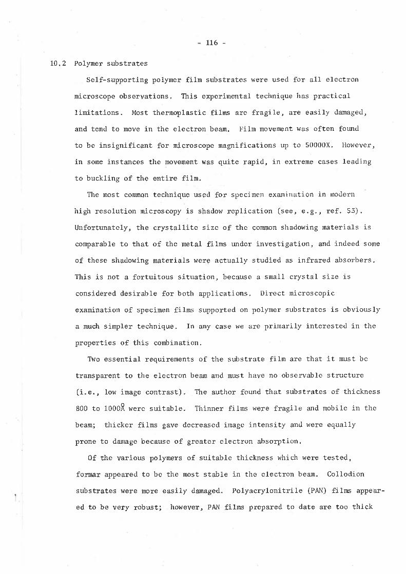
t0.2
116 -
Polymer substraÇes
Self-supporting polyner filn substrates were used for all electron
nicroscope observations. This experirnental technique has practical
linitations. Most thernoplastic filns are fragile, are easily damaged,
and tend to move in the electron beam. Filn novement hlas often found
to be insignificant for microscope magnifications up to 50000X, However,
in some instances the movenent was quite rapid, in extreme cases leading
to buckling of thç entire film.
The nost common technique used for specinen exanination in rnodern
high resolution nicroscopy is shadow replication (see, e.g., ref. 53).
Unfortunatoly, tl're crystallite size of the common shadowing materials is
comparable to that of the ¡netal films under investigation, and indeed sorne
of these shadowing naterials were actually studied as infrared absorbers.
This is not a fortuitous situation, because a snall crystal size is
considered desirable for both applications. Direct microscopic
exanination of specimen films supported on polymer substrates is obviously
a much simpler technique. In any case we are prirnarily interested in the
properties of this conbination.
Tlvo essential requirements of the substrate film are that it mrst be
transparent to the electron beam and must have no observable structure
(i.e., 1ow inage contrast). The author found that substrates of thickness
800 to 1000R were suitable. Thinner filns were fragile and rnobile in the
bean; thicker filns gave decreased image intensity and were equally
prone to danage because of greater electron absorption.
0f the various polynerg of suitable tl'rickness which were tested,
formar appeared to be the rnost stable in the electron beam. Collodion
substrates were ¡nore easily danaged. Polyacrylonitrile (PAN) filns appear-
ed to be very robust; however, PAlrl films prepared to date are too thick
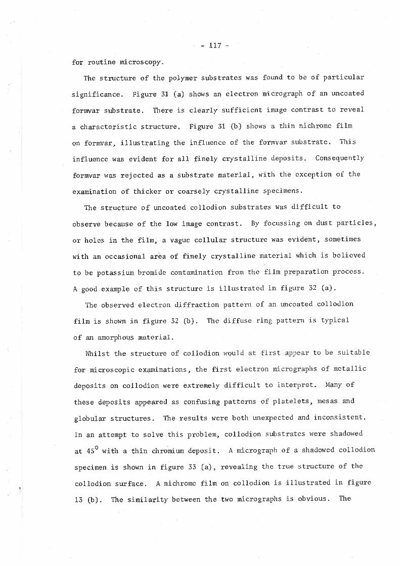
-tL7-
for routine rnicroscopy.
The stnrcture of the polyner substrates was found to be of particular
significance. Figure 31 (a) shows an electron nicrograph of an uncoated
forrm¡ar sr¡bstratç. There is clearly sufficient inage contrast to reveal
a characteristic structure, Figure 51 (b) shows a thin nichrome filn
on fornvar, illustrating the influence of the forrnvar substrate. This
influence was evident for all finely crystalline deposits. Consequently
fornvar was rejected as a substrate naterial, with the exception of the
exanination of thicker or coarsely crystalline specimens.
The structure of urcoated collodion substrates was difficult to
observe because of the low irnage contrast. By focussing on dust particles,
or holes in the filrn, a vague cellular structure was evident, sometimes
with an occasional area of finely crystalline naterial which is believed
to be potassium bromide contanination fron the fíln preparation process.
A good example of this structure is illustrated in figure 32 (a) -
The observed electron diffraction pattern of an uncoated collodion
film is shown in figure 32 (b), The diffuse ring pattern is typical
of an amorphous material.
Itltrilst the structure of collodion wguld at first appear to l¡e suitable
for microscopic exaninations, the first electron micrographs of netallic
depOsits on collodion wele extremely difficult to interpret. Many of
these deposits appeared as çonfusing patterns of platelets, mesas and
globular structures. The results were both unexpected and inconsistent.
In an atteÍpt to solve this problern, collodion substrates ulere shadorved
at 45o with a thin chroniun deposit. A nicrograph of a shadowed collodion
specinen is shown in figure 35 (a), revealing the true structure of the
collodion strrface. A nichrome filn on collodion is illustrated in figure
LS (b). The sinilarity between the two nicrographs is obvious. The

(a) Formvar substrate. Mag.20000X
oO) 70Ã nichrome film on formvar' Mag.20000X
Neg. No. 301 I
Neg. No. 969
Figure 31. Structure of formvar substrates
(a) Collodion substrate. Mag. 20000X
(b) Collodion electron diffraction pattern
Neg. No. 1045
Figure 32. Structure of collodion substrates
Neg. No. 1046

(a) Collodion substrate shadowed with chromium. Mag' 20000X
(b) Thick nichrome fìlm on collodion. Mag. 20000X
Neg. No. 1053
Figure 33. Influence of collodion substrates in electron microscopy
Neg. No. 2913
10. 3
118 -
large ilmesail structule in both cases is of size 0.1 to 0.5 ¡rm. A
careful study also reveals a fine filamentary structure, of dianeter
approxinately 50 to 50R, which is believed to be nolecular chains
in the collodion substrate.
The anonalous structural effects described above were observed only
with the finely crystalline, higher melting point netals studied in the
proejct. This phenomenon is now considered to be the result of substrate
heating during deposition, causing substrate distortion with a consequent
shadowing (or pseudo-shadowing) action. It is also felt that sinilar
conditions, prevailing in experinents carried out by various authors
(see e.g., references 26, 27) na;y have lead to previous misinterpretations
of observed structures.
Structure of gold films
Gold filn infrared absorbers alcl bolo¡reter detectors have been used
extensively in the authorrs laboratory. Electron nicroscope exaninations
have added considerably to ouï understanding of the physical properties
of these filns. Figure 34 shorvs electron micrographs of two gold films
of thickness (a) fOSR and (b) 250R. The filns are seen to be coarsely
crystalline aggregates. l?rinner films are agglonerates which grow into the
structqre illustrated in nicrograph (a), a typical structure observed for
the maxinum measured infrared absorption. The characteristic "fissuresrr
are gaps in the gold film (not the substrate). The fissures are gradually
filled as deposition continues, to give the structure shown in micrograph
(b). Figure 35 (a) is a high rnagnification reproduçtion of a 165R thick
filn. The individual crystallite size is approximately 200R.
An electron diffraçtion pattern of a 32OR thick gold filn is given in
figure 55 (b) . The ring pattern is indicative of a polycrystalline film.
The rings are sharply defined because of the la¡ge crystal size, and the
squales of the radii are in the sequenÇe 3, 4, 8, 11, which is characteris-
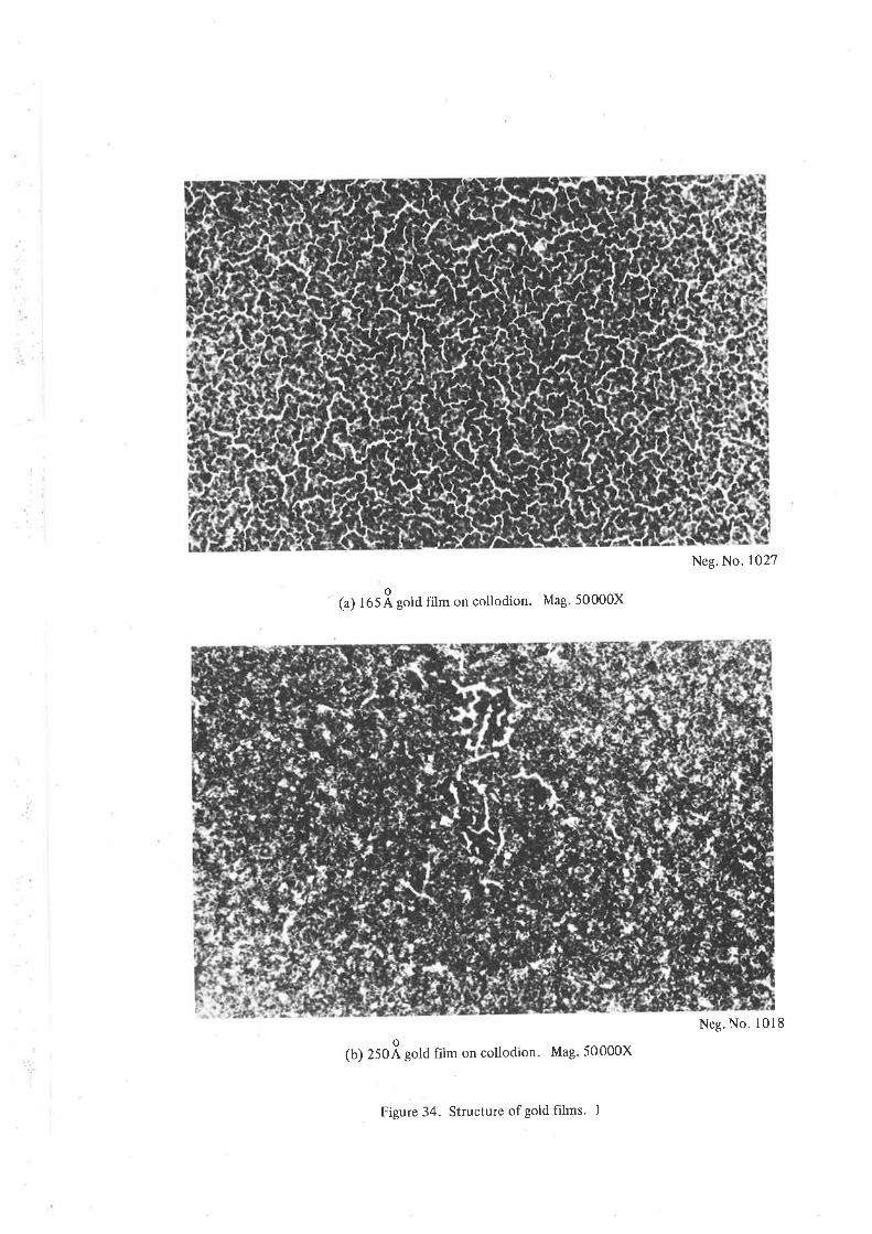
' (a) 165Ãgold film on collodion. Mag. 50000X
o(b) 250Ã gold film on collodion. Mag. 50000X
Neg. No. 1027
Figure 34. Structu¡e of gold films. I
Neg. No. 1018
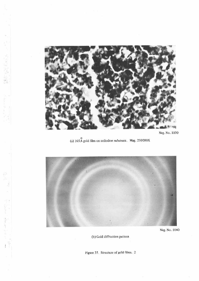
ð.f
(
t
*rlNeg. No. 1030
:r.
ffi
(a) l65A gold fìlm on collodion substrate. Mag. 250000X
(b) Gold diffraction pattern
Figure 35. Structure of gold fìlms. 2
Neg. No. 1040
119 -
tic of the expected face-centled cubic lattice. The rings appeared
sharper in the electron rnicroscope - the rnicrograph is overexposed.
The diffuse background is a consequence of the collodion substrate.
The electron micrographs are identical in appearance to specirnens
prepared by Pashley et al on carbon substrates (ref . 22, figure L2) .
Similar structure has been observed for gold filns deposited on to both
borosilicate substrates (ref. 55), and rock salt substrates at room
temperature (ref. 23).
Three important observations with the electron microscope have shed
light on the infrared absprl-rer characteristics of gold films :
(a) A change in crystal structure is often observed soon after
exposure to the electron beam. This pherìomenon has also been
noted in early work by Levinstien (ref. 26). Crystal re-orientation
is caused by bearn heating, a¡rd is an indirect confirnation of the
postulate of rrcurrent agingrr discussed in Section 7.2.
(b) There is clear evidence of the influence of deposition rate on filn
properties. Thus a filrn forned by very slow deposition became
electrically conducting at roughly twice the thickness of films
prepared in the nornal manner. The film was, however, sinilar in
appearance to the thinner films, indicating a preferred upward
grot4/th. When conduction commenced the film was, at that stage,
almost a perfect infrared reflector.
(c) The characteristic I'fissuresrr in tl're nicrograph, figure 34 (a), tr'ere
observed tg be areas of mechanical weakness in the gold filns. Filns
were seen to fracture along these fissures under the action of the
eleçtron beam, suggesting a stress concentration. This structure
is typical of filns having mâxinum infrared absorption, and thus it
imposps a linitation on the operating temperature of gold filns on
10 .4
L20 -
collodion substrates.
It is not surprising that it is difficult to prepare gold films of
precisely deter¡nined electrical characteristics. The slightest change
in growth pattern nay car¡se, for films of the same thickness and optical
properties, a difference in sheet resistance of m¿ny orders of magnitude.
The discontinuous nature of thin gold films nust account, at least
in part, for the reduced fil¡n density noted in Section 7.1. This is an
irunediate conseguence of the fact that the Tolansky intefferorneter measures
the average thickness of thin filns.
Structure of nichrone films
The structure of nichrome films has been investigated in several
laboratories, the best known work being that by Bricknell et a1 (ref. 56).
These authorfs postulated that the films are composed of nickel rich
islands separated by a continuous chrornium oxide skin. The island size
was approxinately 100R, whilst the individual crystallites were less than
fOR in dianeter. This is in agreement with our earlier discussion of the
influence of oxidation on the formation of nickel and nichrome filns
(Section 9.3). The author has found no evitlence, front his orvn study of
nichrome filns in the electron microscope, of a structure in contradiction
to this general description.
Figure 36 (a) shows an electron nicrograph of a nichrome filn on a
collodion substrate. The filn is seen to consist of a fine island
structute, sone of larger size and thicker (higher contrast). The most
notable difference fron the work of Bricknell et al is that the island
size is much snaller - only the largest has a dinension of approximately
100R. This is not surprising, as the Bricknell study applies to cleaved
rock salt substrates at a substrate tenperature of 27OoC. Because of the
inherent complexity of the structure of nickel-chrorniun fil¡ns, and the

-1
o(a) laOÃ nichrome film on collodion. Mag. 100000X
o(b) 125 Ã nichrome film on collodion. Mag. 200000X
Neg. No. 987
Fþre 36. Structure of nichrome films
Neg. No. 972
10.s
l2r -
ample descriptions reported in the literature, no effort was made to
extend this study,
Figure 36 (b) shows a thin (200f¿ per square) nichrome fílm on a fornvar
substrate, at high magnification. This rnicrograph is of interest because
of the evidence of botl'r "filanentaryrr structure and the larger scale
I'cellularrr structure in the polyner filn.
Struçture of nickel filns
The examination of nickel filns in the electron microscope was hanpered
by the difficulty of preparing specimens which were totally free of
structural influence fron the polyrner substrate. This problem was also
experienced with nichrome films. In general, it was found that films
of sheet resistance of less than 200f¿ per square showed sone sign of danage
from the deposition process, and almost invariably revealed the
characteristic substrate structure. Iligh pohrer conventional microscopy
has shown that thicker nickel films prepared by electron beam deposition
on Srnm grid carriers were usually buckled or partially destroyed. A
sinilar result was observed for platinun and chronium films. Because of
more effective heat sinking, the grid ca:rier specinens survived deposi-
tion, whereas the larger specimens prepared for optical measurement were
often destroyed.
The structure of a nickel film of thickness 350R deposited on to a
collodion substrate is illustrated in figure 37 (a). The filn is seen to
be finely granulated, the naxinun size of the crystallites being approxi-
mately 50R. Because of this fine structure it was often difficult to
achieve an accurate focus. A sinilar "pepper pattern" appearance was
also observed for chromiun and platinun filns.
Neugebauer (refs . 34, 57) found that for 1OOR thicl< nickel filns on
glass substrates, there was no evidence of aggregations into islands,

o(a) 350Ã nickel film on collodion. Mag' 100000X
Neg. No. 1038
(b) Electron diffraction pattern of partially oxidized nickel film
Figure 37. Structure of nickel fìlms
Neg. No. 1048

122 -
a¡rd the filns appeared continuous. These filnls tvere prepared in ultra
high vacuo. Fleet (ref. 33) found a çrystallite size of 60R for glass
and silica substrates at room temperature. Levinstien (ref. 26) also
observed a finely crystalline structure for nickel on collodion substrates.
These latter results are in agreernent with the authorrs recent study.
0n the other hand, Sennett and Scott (ref. 27) noted an aggregated structure
for filns on formvar substrates. These authors shadowed their specinens
to demonstrate that aggregation was not caused by electron beam interaction,
but may have overlooked the possibility of structural anomalies introduced
by the extrenely thin formvar substrates.
Electron diffraction patterns for nickel films on formvar and- collodion
substrates weïe not as sharp as that of gold (figure 34), indicating
either a snal1 crystallite size oT a crystallite size significantly
different fron island dinensions. The ring radii confirm the face-
centred cubic lattice for nickel. An eleçtron diffraction study of a
thick semi-insulating filrn prepared at a slow deposition rate (figure 37
(b)) indicated a change in the ring pattern which, frorn a study of the
reports by several authors on artificial thernal aging of metal fi1ns,
would suggest the presence of an oxide phase. A quantitative analysís was
not carried out.
The influence of stress in nickel films is apparent in the nicrograph
figure 38. The micrograph shows an inperfection in a nickel filn on a
formvar substrate. The tear in the film probably originates frorn a flatv
in the substrate, ild the weakening (of the substrate) has caused the
nickel filn to part, presumably under the influence of bean heating.
The strbstrate can be seen stretched across the gap in the filn, and the
stress is clearly tensile. This observation would appear to support the
proposed mechanism for stress in nickel fihns discussed in Section 9.4,

Neg. No. 1074
o1954 nickel fìlm. Mag. 50000X
Figure 38. Stress in nickel film on formvar substrate
10.6
L23 -
although it should be noted that we have found no evidence of gross
imperfections in the rrstress-relievedil fiIns.
A further examination of figure 38 reveals the fine filanentary
structure in the fornvar substrate, described earlier in Section 10.2.
The characteristic fine-grain structure of the nickel filn is also clearly
dis cerned.
Relationship between structure and film properties
This study has afforded considerable evidence, albeitof a qualitative
nature, of the relationship between film structure (as observed in the
electron nicroscope) and the various filn properties discussed in
preceding sections.
Electron nicroscope exaninatlons have enabled us to explain, with
increased confidence, tlle reasons for the failure of the electrical-
optical relationships for gold absorber filrns, and also the change in
fihn properties with deposition parameters.
The study of the structure of the higher rnelting point evaporants has
tended to confirln our evaluations of the suitability of these naterials
as infrared absorbers, notably that smal1 crystallite size is conducive
to a more predictable absorber, and that a nuch thinner film can be
realised.
The problen of stress in thin filns of higher nelting point naterials
has been clarified.
When we take the observed physical properties of the thermoplastic
substrates into consideration, we may deduce that future research should
proceed along the following lines :
(a) We should seek a new substrate film, which is capable of withstanding
a higher te¡nperature and does not swell or stretch. A thermoplastic
material such as polyacryonitrile, which can be partially pyrolised

-L24-
without change in composition, nay be suitable. Alternatively, a
ilcross-linkedfr naterial ¡nay prove to be satisfactory.
(b) The filn should be cooled during deposition, e.9., radiation cooling
to either a dewar or thermoelectric cooler'
(c) Cooling of the film will not reduce, and indeed may enhance, filrn
stress. Therefole l4te must seek a stress release mechanism' Our
experience would indicate that lrigh voltage rrcurrent agingrr during
the initial coalescence phase nay be appropriate. stress relief
may also be inherent in the electron bean deposition plocess,
provided that an inproved substrate naterial is available.
(d) In order to reduce oxidation and to realise the snallest possible
crystallite size, the deposition rate should be increased, and
preparations carried out in a highel vacuun. unfortt[rately, there
is a practical limit to rate of roughly 2000R.m-1, set by the
accePtable monitoring time'
FinalIy, we have the satisfaction of justification of our earlier
predictions on the structure of the selected infrared absorber materials'
We are now able to procqed with confidence to the study of new and
probably superior absorber naterials such as platinun and palladiurn' These
materials are readily prepared by means of electron beam deposition'
11. I\EASUREI"IENT OF T]IERMAL PROPERTIES
Measurenents v¡eÏe nade of the tempeÏature coefficient of resistance,
temperattrre rise, thermal rise tine and thernal spread of rnetal absorber
films. A radiometer test apparatus has been constlucted for the measulement
of therrnal properties of thin films. This instrument cornprises a notol-scanned
sanple stage, a fast-response infrared radiometer and a miniature blackbody
cavity. Unfortunately the apparatus is still in the developnental stage and
precision measure¡nents ale not yet available. All thernal measurements reported

-LzS-
in this thesis were carried out using variot¡s indirect experinental techniques,
whereby temperature rises hrere generated by Joulc hcating in the absorber film.
Thus radiant power was sinulated by an electrical analogue.
11.1 Theory of the electrical analogue technique
In all of the techniques described in this section, radiant energy
absorption was sinulated by the application of a d'c' or pulsed voltage
to a specially shaped absorber elernent. This in no way conplicates the
theoretical analysis. The only change to the derivations of Section 2
is that the absorbed power, AP, appearing in the expression for maximum
temperature rise (equation(20)) takes the form :
Ap = I2R (119)
wherelistheaverageçurlentpassingthroughtheelement,andRis
the average resistance of the elenent.
11. 1.1 Thernal sPread
Ther¡nal spread can be measured by passing a steady cu:rent
through an appropriately shaped element, then scanning the
specinen with a high resolution radiometer. The nagnitude of
the tenperatule rise need not be known; however, if the radio-
meter is calibrated, then a direct measurement of tenperature
rise can be recorded during the scan'
11.1.2 Ttrermal rise time
Thernal rise time can only be measured directly with the above
' instrurnentation if the response tine of the radiometer detector is
very nuch snaller than the tine to be observed. Ifrhowever, the
element is pulsed, then the thermal tine consta¡rt can be determined
by rneasurenent of the change in resistance with tempe1'ature' The
actual tenpeÌature again need not be known but if the temperature
coefficient of resistance is measured, then the ave1age terÌpe1atule

-126-
can be determined during the sane experiment.
Let us assume that a current, I, is applied to the absorber
elenent from a voltage supply of output resistanc" RL. As the
temperature of the elenent rises through Joule heating, its
resistance, R, increases by an increnent AR (the netal film has
a positive tenpeÌature coefficient of resistance), and the
voltage drop, V, across the elenent rises by an increnent AV.
The voltage ri.se is given by
AV= V+
RIAR IR+AR+RL
(t2o)
where Vo is the source voltage. If the average temperature
rise, AT" is small, then
AR = RoAT, (LZI)
where o is the tornperature coefficient of resistance (of-l). If
we make R¡ very nuch larger than R (i.e., a constant current source),
then
,
AV= IqAT
3 RIcTAT^ (L22)a
This is the rise in voltage over a period which is long conpared
to the thernal rise time (we assume that the pulse length is r,ruch
larger than the rise tine). The time dependent voltage rise is
simpLy
ÀV = RIcAT, (l-expGt/r)) (L23)
where t is the thernal rise tine.
Thus measurement of the voltage rise yields a value of the
B¡LR+RL a
It.2
_ L27
thernal rise tine for the absorber film. If the thermal spread
is small compared to the element dimensions, t is just the time
constant given by equation (26). 0thenvise, r is the rise time
corresponding to the average tenperature tise, and can be
computed fron the theo¡y of Section 2.3.3.
If the temperature coefficient of resista¡rce of the absorber
filn is known, the average temperature rise can be deternined
during the sane experiment fron equation (I2l).
Specimen preparation
The specinens prepared for the neasurenent of thennal properties
were briefly described in Section 5.3.6. Absorber filns were deposited
on to 850R thick collodion menbrane substrates. Substrates u¡ere
mounted on either 25 mn o.d. x 20 nn i.d. epoxy annuli or 25 mn
dianeter slotted epoxy discs. Evaporation masks were shaped to provide
metal specinen films of size 12.5 nm long x 2.5 nrn wide for the a¡rnuli
or 2.5 mrn square for the slotted discs. We would expect the tenperature
rise and thernal rise time for the large elements to apploach the
maximum values determined by radiation loss only. However, for the
snaller elements, conduction loss to the film mount will reduce the
nagnitudes of the temperature rise and rise time, depending on the value
of the thernal spread constant.
Some relevant paramgters of the eight specimens selected for study
are listed in Table 4. It will be noted that resistance is given as ohm
per square, Rs, whereas the actual resistance of the large specinens is
SRr'
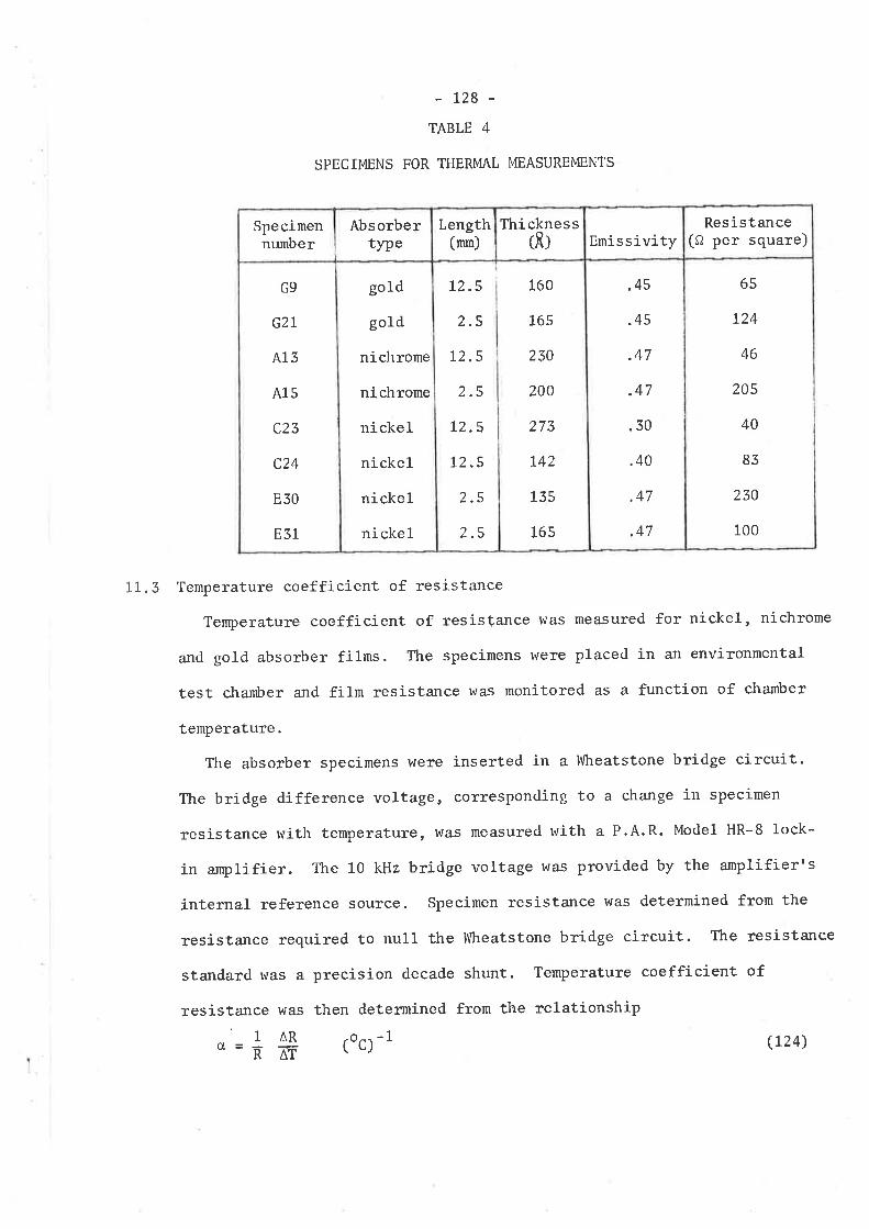
11.3
-728-TABLE 4
SPECIMENS FOR TIIERMAL MEASUREMENTS
65
L24
46
205
40
85
230
100
.45
.4s
.47
.47
.30
.40
.47
.47
t2.5
2.5
t2.5
2.5
L2.5
t2.5
2.5
2.5
160
16s
230
200
273
L42
L35
16s
gold
gold
nichrone
nichrone
nickel
nickel
nickel
ni cke I
G9
G2T
A15
A15
c23
c24
E50
85L
Resistance(a per square)Emissivity
ThicknesstRt
Length(trun)
Absorbertype
Specimennumber
Temperature coefficient of resistance
Temperature coefficient of resistance was measured for nickel, nichrome
and gold absorber fi1¡ns. The specimens were placed in an environmental
test chanber and film resistance was nonitored as a function of chanber
temperature.
The absorber specimens h¡ere inserted in a ltlheatstone bridge circuit.
The bridge difference voltage, coïresponding to a change in specirnen
resistance with temperatuïe, $Ias measured with a P.A.R. Model HR-8 lock-
in amplì-fier. The 10 kHz bridge voltage was provided by the amplifierrs
internal reference source. Specinen resistance was deternined fron the
resistance required to nul1 the Wheatstone bridge circuit. The resistance
standard t{as a precision decade shunt. Tenperature coefficient of
resistance was then determined fron the relationship1
^R (oc) -1 (L24)O=F ãT
I29 -
An innediate difficulty was encountered when rneasure¡nents were made
of the resistance of the specinens listed in Table 4. Accurate nu1I
readings could not be obtained because of an excessive noise level.
The noise was found to be caused by fluctuations in the resistance of
the specimens. The fluctuations were greatest for the 12.5 nm absorber
filns , and reliable neasurenents of the ternperature coefficient of
resistance could not be obtained for these specirnens. This problern was
not evident when measurements were nade of the resistance of either
very smal1 absorber elenents or of netal films deposited on to glass
substrates. There appeals to be little doubt that the excess noise
level is caused by tl-re 'rstrain gauge'r effect.
Because of the above difficulty, only linited data were obtained of the
temperature coefficient of resistance of the eight selected specinens
listed in Table 4. The temperature coefficient of 2.5 nn gold and
nickel absorber specinens was found to lie in the range 0.5 to 1.0 x 10⁻⁵
oC-1. The temperature coefficient of a nichrome specimen was less than
0.5 x 1.o-3 0a-1.
A new series of experiments has been cornrnenced to deternine the
temperature coefficient of resistance of 0.2 mn x 0.05 mn gold and
nickel bolometer elements. The resr¡lts obtained so far indicate that
the tenpeïature coefficients of filns of similar thickness to the
specinens listed in Table 4 lie within the range of values given above.
The bulk tenperature coefficient of resistance of gold and nickel is
approxinately 4 x 10⁻³ oa-l and 6 x 10⁻³ oc-1 r"spe"tively. The lower
values observed for thin films are to be expected, and indeed are
predicted by the Fuctrs-Sondhiener theory (Section 3.5). It is of
interest to note that neasurements rnade on nickel films yieLd further
inforrnation on the influence of fi1¡n oxidation. Thus Reale (ref. 58)

Lt.4
130
has measured a tenperature coefficient of 1.2 x 70-5 oc-l fo" nickel
filns of thickness 2000R to 5000R, and has deduced that the oxide
content of these filns is approxinateLy 3.5%. Tl're nethod of prepara-
tion was not stated in the reference. However, the trend is clear :
in addition to rrsize effectrr, film oxidation contributes to a decreased
temperature coefficient of resistance.
IrÍeasurement of thernal rise tine
A relatively sinple technique Was devised for tho measurenent of
thermal rise tine. This technique nakes use of the electrical analogue
discussed in Section LL.L.2.
A test current was applied to the specinen film fron a Data-pulse
Irtodel 1004 pulse generator, and the voltage drop across the specimen
was displayed on a Tektronix Type 5648 plug-in storage oscilloscope.
The vertical deflection plug-ín trnit was a Type 349 differential
anplifier. This anplifier has a high connon-mode-rejection-ratio,
ranging fron 300 at 10 Hz to 200000 at 1 kHz. The neasurement circuit
was arranged such tllat the specinen forned one arm of a lVheatstone
Bridge. A precision decade shunt was inserted in a second arm of the
bridge, and the voltage drop across this shunt (the rTeferencer voltage)
was applied to the alternate channel of the amplifier. The two
renaining resistances in the bridge were of equal nagnitude, and were
used to set the test current. Thus, when operated in the differential
mode, the oscilloscope displayed the bridge difference voltage, the
desired wavefor¡n being achieved by adjusting the reference channel
voltage. The oscilloscope time base was externally triggered fron the
pulse generator.
The specimen was evacuated to 2 x 10⁻⁶ torr. A 100 ms or 250 ns
square wave (chosen so that the period was large conpared to the
T3L
observed rise tine) was applied to the measurement circuit. The test
current was set to a suitable peak value, usually 1.0 to 2.0 mA. Wit}t
the anplifier in the differential mode, the reference voltage hlas
adjusted to display a null at the traillng edge of the pulse. A
typical waveforn is illustrated in figure 39(a). Figure 39(a) represents
thernal decay, the leading edge corresponding to the increnental
resistance AR in equation 121. This display was preferred to the rising
waveforn, shown in figure 39(b), because of greater null stability.
The display was photographed using a Tektronix Type C-12 oscilloscope
camera and the thermal rise time determined as the tine to rvhich the
u¡aveform decayed to I/e of the initial value. At least two measurements
were nade of each specirnen, yielding an estimated accuracy of ! 0.05 tine
base divisions (e.g,, t 1 rns for 20 ns/div).
This technique was found to be a rapid and sensitive method of
estinating the thernal time constant of infrared absorber and bolometer
detector elenents. Because of the low signal levels, particular care
was required to mininize pick-up and earth loops.
Lt.4.1 Theoretical predictions
The therrnal rise tine was computed for each specimen frorn the
theory of Section 2. We should recall that the rneasured rise
tine approximates the sirnple time constant, given by equation (26),
only when the element size is large compared to the thermal spread
constant, i.e., for radiation loss only. IVhen conduction loss
becomes significant, the rise time ¡nust be conputed fron the tine
dependent equations given in Section 2,3.3, The selection of the
l/e ordinate as the reference for rise tine measurements is useful
for comparison purposes, but should not be taken to inply a simple
exponential law. Equation (123) is thus an epproxination.

(a) Thermal decay
(b) Thermal rise
Specimen C24
Scale: 50ms/div (horizontal)500¡rV/div (vertical)
¡¿..r..4-f
,
1
Figure 39. Thermal rise time measurement. Oscilloscope display
7t.4.2
7L.4.3
-L32-
The rise tine was deternined by computer cornputation of the
tirne dependent average temperature rise, initially by assuning
the bulk properties listed in Table 1. The renaining relevant
parameters (deternined experimentally) are listed in Table 4.
The conputed rise time was then compared with the experirnentally
deternined value. I¡lhere necessary, the computation hlas repeated
to determine the value of specific thernal capacitance (density
and specific heat) and thennal conductivity required to effect
agreenent with the measured value.
Influence of background ternperature variations
An acÇurate rneasurement of the background temperature, To, was
not nade; however, this should not be significantly different
to room tenperature. The average laboratory tenPerature
(controlled to ! 2oC) was 295oK. The cornputer program provides
for a fixed value of To of 300oK; thus an error will occur in
the detern-ination of rise tirne. It can be readily shown fron
equations (6) and (26) that the naximum error fron this cause
in the calculation of rise tine is approximately 5e', ild in this
case the computed value will be lower than the actual value. A
similar er.ror rvill be incurred in the estimation of temperature
rise.
Influence of the linear radiation loss law
The assumption of a linear radiation loss law also leads to
erroTs in the conputation of both temperature rise and thernal
rise tine. Fron equations (2), (5) and (6) it is easily shown
that for a temperature rise of 10oK above a background at 300oK,
the naxinum errol is again approxinately S%, but here the computed
value will be higher than the actual value.
17.4.4
11.4.5
- 135 -
The author has concluded that the overall error due to the
above considerations lies within the accuracy of measurenent of
thermal rise time, the two errors being compensatory.
Influence of an imperfect heat sink
In the analysis of the thernal properties of the selected
specimen films, it is assu¡ned that the epoxy mounts act as
perfect heat sinks. In order to test this assunption, the
thermal waveform was stored on the oscilloscope for a period of
at least 2 minutes after applying the pulse bias. It was found
that the temperature Tose by at rnost 5% of the initial vaLue,
indicating slight heating of the epoxy mount; however, the error
in rise tine was within the accuracy of the measurement technique.
Influence of chamber pressllre
A rise in chamber pressure has a dramatic effect on the observ-
ed thernal rise tine. This observation is not unexpected, and is
caused by the contribution of gaseous conduction and convective
heat loss to the thermal surface conductance. At high chamber
pressures these losses are much larger than radiation 1oss.
Careful measurements were nade of temperature rise and thermal
rise time as a function of clianber pressure. It was found that
the ternpefature rise and rise tine were constant (within measure-
ment accuracy) at pressures less than 1 x 10⁻⁴ torr. Frorn
approximately 5 x 1O-4 torr to 1.0 torr both parameters decreased
rapidly, thenceforth falling s1owly fron 1.0 torr to atnospheric
pressure. The following values for rise tine (specinen E31)
were typical z
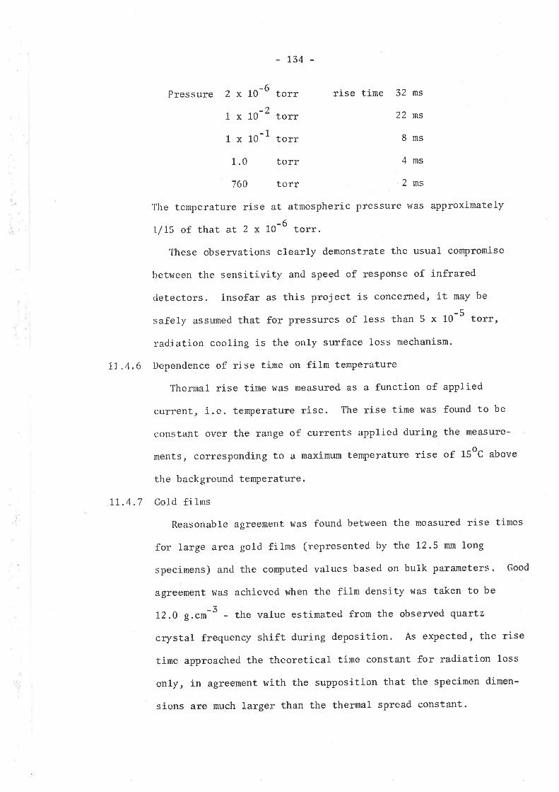
t34 -
Pressure 2 x 10⁻⁶ torr rise time 32 ms
1 x 1o-2 ,ort 22 ms
1 x 10⁻¹ aott 8 ms
1.0 torr 4 ns
760 torr 2 ms
The temperature rise at atmospheric pressure was approximately
1/15 of that at 2 x 10⁻⁶ torr.
These observations clearly demonstrate the usual conpronise
between the sensitivity and speed of response of infrared
detectors. Insofar as this project is concerned, it may be
safery assumed that for pressures of ress than S x 10-5 torr,
radiation cooling is the only surface loss mechanism.
II.4,6 Dependence of rise time on film temperature
Thernal rise time was measured as a function of applied
current, i.e. teÍperature rise. The rise tine was found to be
constant over the range of currents applied during the measure-
ments, corresponding to a maximum temperature rise of 15oC above
the background temperature.
Lt.4.7 Gold films
Reasonable agreement was found between the neasured rise tines
for large area gold films (represented by tli'e I2.5 nn long
specimens) and the conputed values based on bulk paraneters. Good
agreement was achieved when the film density was taken to be
12,o g."t-3 - the value estinated fron the observed quartz
crystal frequency shift dUring deposition. As expected, the rise
tine approached the theoretical tine constant for radiation loss
only, in agreenent with the supposition that the specinen dimen-
sions are much larger than the thermal spread constant.
-135-The neasured rise ti¡nes for 2.5 nn specinens were in poor
agteemelìt witlt the computed values, incLuding computations
corrected for filn densíty. The neasured values were higher;
hence hre may suppose that the difference is due to reduced
thernal conduction to the filrn mowrt. Computations indicate
that a ther¡na1 conductivity of 1.0 to 1.5 W(crn.oC)-l, i.e.,
one-third to one-half the bulk value, yields the correct rise
tine. This result is in agreenent with thermal spread neasure-
ments (see Section 11.5.3).
The time dependent average tenperature rise in vacuo for a
2.5 n¡n specimen is illustrated in figure 40. The various computa-
tions discussed above are shown in the figure. The influence
of thermal conduction loss is clearl¡r indicated.
A sunnary of rise time measurenents is given in Table 5. Three
values of rise time are listed¡ the calculated rise time, rc, the
rise tine for radiation loss only, tr, and the measured rise tirne,
rm. The contputed values shown in the table are corrected for
estimated metal film density, but are not corrected for thermal
conductivity.TABLE 5
SUMMARY OF THERMAL RISE TIME MEASUREMENTS
34
22
36
32
63
37
3t
32
35
15
44
39
70
45
30
31
39
39
45
43
74
47
JI
39
L2.0
12.0
6.4
6,5
6.5
6.0
4.0
4.5
gold
gold
nichrone
nictrrone
nickelnickelni ckelnickel
G9
G2T
A13
A15
c23
c24
E30
E31
Tm
(ns)
T c(ns)
1r(ms)
Estimated_density(g.
"r- 3)
Absorbertype
Specinennunber

aTa(t)Araþ")
0.6
o4
1.0
0.8
o.2
1.0
0.8
0.6
0.4
0
Ara(t)
At. {"")
20 40 60 80
Time (ms)
Figure 40. Thennal rise tinre for a gold absorber fìhn
20 40 60 80
Time (ms)
Figure 41. Thermal rise time for a nickel absorber fìlm
0.
0
W
Specimen G21Length 2.5mm
1. Corrected density2. Corrected density3. Corrected density4. Radiation loss only@ Measured data
Substrate: Collodion 85OÅ
K=2.0K= 1.0
.4/,
4o
1
3'
I
/
Specimen E31Length 2.5mm
1. Corrected density2, Bulk density3. Corrected density K = 0.064. Radiation loss onlyo Measured data
Substrate: Collodion 8b0Å
/;
ro
I
*¿
100
11. 4. I
11 . 4.9
-L36-
Nichro¡ne filns
Measured rise tines for two specimens are listed in
Table 5. The measured rise tines are seen to be 7 to 8 ns
lower tha¡r the calculated values, which are based on the
bulk value for thermal conductivity. It is hrorthy of note
that the thickness of both specinen films is larger than
films of the sane sheet resistance prepared at an earlier
stage of the research progran (see Section 8), probably
because of deposition in a poor vacuun. The composition
and structure of these filns is therefore uncertain.
Nickel films
Thermal rise time data for four nickel specimens are
listed in Table 5. Reasonable agreement was again found
between the measured rise tines and the computed values,
assuning a corrected filn density derived fron quartz
crystal frequency shift data during deposition.
The tine dependent average temperature rise in vacuo
for a 2.5 run long nickel film is illustrated in figure 41.
The influence of the corrected density is clearly shown.
It should be noted that this correction implies a decrease
in thermal capacitance, a quantity which also includes the
specific heat of the filn. We cannot say with certainty
that the decreased thermal capacitance is due to density
alone, only that the evidence points to this conclusion;
hence the specific heat is presunably not nuch different
to the bulk value. Partial oxidation of the nickel film
would not significantly alter the results because the
density and specific heat of NiO are not greatly different
11.5
L37 _
to nickel neta1.
It will be noted in Table 5 that the conputetl rise times
for the 12.5 mm specinens are larger than the neasured
values, whereas the predictions for the 2.5 nm specirnens are
smaller. However, when a correction is applied for thernal
conductivity (deduced from thermal spread neasurenents), as
shown in figure 41 for specimen E31, the conputed rise tirne
is increased. The corrected value for specimen ES1 is
56 ms. This general trend is evident throughout the
measured results, ild is probably a consequence of the
selection of 2.25 J."r-3'oc-1 fot the product of density
and specific heat of the collodion substrate. Examination
of the published bulk data for cellu1ose nitrate shows that
this product can vary fron L,7 to 2.7. A value of 1.9 to Z.O
is required to achieve agreement betleen the computed and
measured rise tirnes, for the specirnens listed in Table 5.
In the light of the above discussion, it is significant
that agreenent between theory and experiment can be
real.ised by applying corrections to the thermal capacitance
and thermal conductivity of the netal absorber filn alone.
This impl.ies that the thernal properties of the BSOR thick
polyrner substrate are not significantly reduced fron the
bulk values, a result borne out in earlier work by one of
the authorrs associates (ref,2).
Measurenent of thermal spread
Measurements were made of the thermal spread in gold, nicl<el and
nichrone absorber films. The thermal spread constant, x, was
determined for each specimen and estimates were ¡nade of the thermal
_138_
conductivity. The rneasurenent technique and experimental results
are described below.
11,5.1 Thernal spread apparatus
Thernal spread hras measured with a high-resolution
scanning radioneter. This instn¡ment was constructed in
the authorrs laboratory (ref.59), and has been used in
earLier researÇh on thermal spread in thin mernbranes (ref.2)
Tlre infrared radíorneter is cornprised of an f/t, 4X
nagnifícation, nonocentric optical systen, a thernocouple
detector and an 11.5 Hz mechanical chopper assernbly. The
specinen is mounted in a precision sanple holder, which
remains stationary during operation, Ðd the entire
radioneter assenbly is nade to move, by means of a sma1l
rnotor drive turit, in the horizontal direction. Optical
focus and scan position can be accurately located by neans
of nicroneter drums. The maximurn scan amplitude is 5 nn.
The scan rate is 165 prn.rnin-l and the optical resolution,
measured in the specinen plane, is approxinately 0.05 nun
along the direction of the scan motion.
In the present experinents the detector output was
connected to a P.A.R. It{odel HR-B lock-in amplifier, with the
arplifier phase-locked on to the chopper reference, and the
output was displayed on a Goerz Minigor Type RE501
potentiometric chart recorder.
The entire radioneter assembly was mounted in a 30 cn
(12 in) vacuun systen and evacuated to a pressure of less
than 5 x 10⁻⁵ torr. The specimen was heated by applying
a d.c. voltage from a constant culrent power supply, a¡rd a
139 -
radioneter scan was tlìen executed along the desired absorber
axis. The resultant chaït record repïeselìts a plot of steady
State temperature rise versus scan distance'
11.5.2 Theoretical predictions
The steady state tenperature rise was computed for each
specimen from equations (13) and (17). Bulk thernal parameters
listed in Table 1 were used in initial cornputations. The results
t{ere compared with radiometer records and the conputptions
repeated to seek the value of the thermal spread constant, X,
required to effect agreenent with experiment'
The analysis of the thermal spread characteristics of absorber
filns is considerably sinplified if the length of the specinen is
greater than 10x. The thermal spread constant can then be
deterrnined frorn equation (19). This equation ca¡r be expressed
in the forn
Ln(1-AT/AT.) = -x/x (125)
Thus x can be detennined directly from the slope of the log plot of
the radiometer records. The thernal conductivity, K, can then be
estinated from equation (50). An examination of the radiometer
chart record will innediately establish the validity of this
technique for anY given sPecinen.
when the above procedure cannot be applied, ê.g. when the
length of the specimen is less than 10X and hence the nid-point
tenperature does not rise to the naximum value, ATo, then the
esti¡nation of X becomes nore difficult. The simplest approach is
to plot a fanily of curves, each curve corresponding to a given
value ef X, then to seek the best fit with the measured data.
Examination of the radiometer scan records revealed that the

-140-
edge of the absorber filn, where it contacted the epoxy nount,
was not clearly defined, the ternperature rise typically falling
to zero at approxinately 0.1 nn beyond the boundary. T?ris effect
nay be attributed to :
(a) the resolution of the optical systen (0.05 rnm half hlidth),
(b) an imperfect mechanical boundary, determined by the
coarseness of the nachining process, Ðd
(c) an inperfect heat sink (see Section 11.4.4).
Poor boundary definition will doubtlessly affect the accuracy of
the thermal sp::ead conputations. However, considerably greater
sophistication in experinental technique would be required to
achieve substantial inprovement in accuracy.
11.5.3 Gold films
RadiometeT scans were carried out for several 2.5 mn long
absorber specinens. The estinated thermal spread characteristics
for one specinen (G21) are shown in Table 6. In this table xc
is the computed thermal spread constant, based on bulk
paranneters, -d Xn is the value deternined by measurement.
Becar¡se of the high thermal conductivity of gold, the
temperature rise at the centre of the 2.5 mn long specinens will
not attain the maxinum value given by equation (20); hence the
tllermal spread constant was deduced by seeking the best fit rvith
computed tenperature rise curves, as discussed in the preceding
strbsection. The results for specinen GZL are shown in figure 42.
Agreement with theory is achieved for a thernal. conductivity of
approxinately 1.0 W(cn.oc)-1, i.e. one-third of the bulk
conductivity. This result is in accord with thermal rise tine
neasurements. Published data for silver films (ref. 60) would
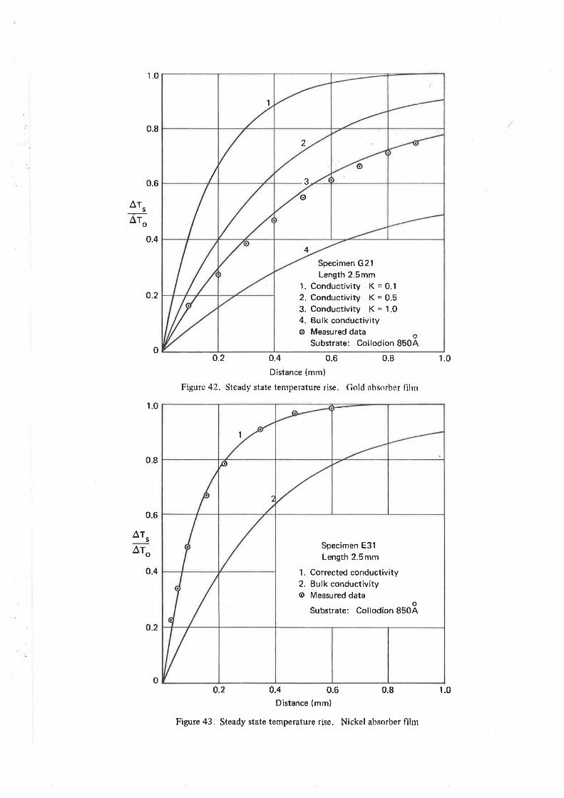
1.0
0.8
0.6
aT.
4o.4
o.2
1.0
0.8
0.6
AT,
aTo
0,4
0
o.2
0
o.2 0.4 0.6 0.8
Distance (mm)
Figure 42. Steady state temperature rise. Gold absorber filrn
o.2 0.4 0.6 0.8
Distance (mml
Figure 43. Steady state temperature rise. Nickel absorber fìlm
1.0
4
Specimen G21
Length 2.5mm1. Conductivity K=0.12. Conductivity K=0.53. Conductivity K= 1.0
4. Bulk conductivity@ Measured data
Substrate: Collodiono
850A
2
3
o
o/
1
Specimen E31
Length 2.5mm
1. Corrected conductivity2. Bulk conductivity@ Measured data
Substrate: Collodiono
850A
p
2
1
1.0
- I41' -
suggest that the above value may be too high'
Spccial 10 run long specimens l¡/ere prepared in an unsuccessful
attenpt to deternine a more accurate value of the thernal spread
constant. The radiometer scan for all specimens showed art
anomalous peak near the ends of the absorber film. This effect
has been observed only for long gold filns.
No predictable relationship has been found between the thermal
conductivity and electrical conductivity of gold absorber speci-
nens. This observation is not surprising, in view of the
electrical properties of these fi1¡ns (Section 7'2)'
TABLE 6
SUMMARY OF THERMAL SPREAD MEASUREMENTS
1.0
0.02
0.03
0.06
550
t02
99
143
949
207
363
400
gold
nichrome
nickel
nickel
G2t
A15
E30
E31
Xm
(um)t
K
tv(cn.oc) -lXç
(un)Absorbertype
Specinennumber
11.5.4 Nichrome filns
Thermal spread measurements rvere made for only one absorber
specinen The results are given in Table 6. The thermal spread
constant was calculated fron the slope of the 1og plot, as
discussed in Section 11.5.2. Note that the thernal conductivity
of the specinen is approxirnately one-fifth of the bulk value.
11.5.5 Nickel filns
Radioneteï scans were carried out for several nickel absorber
specinens. Two specinens, E30 and E51, were studied in depth, with
the results shown in Table 6. The thernal spread in nickel

-t42-
absorber filns was ol¡setved to be nuch smaller than predictions
based on bulk thernal conductivity. This permitted the
determination of the spread constant fron the slope of the log
plot (equation (125)). The thermal conductivì-ty, estimated fron
equation (50), was found to be approximately one-tenth of the
bulk value.
Figure 43 shows the computed steady state temperature rise
for specimen E31. Also shown is experimental data derived fron
radiometer records. The conputed tenperature rise is plotted
for both the bulk and thin filn values of thennal conductivity,
emphasising the decreased therrnal spread in the thin filn.
It is important to note that the lateral thernal conductarice'
Kt, of the nickel absorber is only 4 to 10 times larger than that
of the 850R thick colloclion substrate. This is in marked contrast
to the gold absorbers, rvhere the substrate contribution is snall'
In reaching this conclusion, hle have assumed that the thernal
conductivity of the collodion filn is the bulk value listed in
Table 1. In fact earlier research carried out in the authorrs
laboratory (ref. 2) indicate that the thermal conductivity is
approxinately half the value given in the table. Recent neasule-
nents suggest that the thernal conductivity rnay be slightly higher.
A definite relationship has been established between the thermal
and electrical conductivities of nickel absorber films. Wtrilst we
have not discussed the possibility of such a relationship in
earlier sections of the thesis, the free electron theory of netals
predicts that conduction electrons are mainly responsible for the
transfer of heat in netals. In vierv of the success of the infrared
optical theory for nicltel absorber films, as represented by the
-t43-
results shoh¡n in figure 30, we rnight suspect therefore that the
thermal conductivity is also directly related to the neasured
electrical proPerties.
The lViedenann-Franz Iaw states that for a given temperature
the ratio of thermal to electrical conductivity of a netal is a
constant. This constant has been verified by experinent for bulk
netals at room tenpeïature. we would not, however, expect to
find a constafit proportionality between the thernal conductivity,
K, and electrical conductivity, o, of the nickel absorber fil-ns
prepared in this study. l\ie have seen that the ratio of the bulk
to thin filn conductivity, oo/o for films of naxi-num absorption is
at least 20. The nagnitude of this ratio is a measure of the
degree of filn oxidation. Increaçed oxidation can lead to semi-
conducting filrns, fo1' which oo/o is very large (and the infrared
absorption small.). On the other hand, the ratio of the bulk to
thin film thernal conductivity, Ko/K, will have an uppel bourd set
by the phonon contribution to the total conductivity. Thus we
should seek a relationship of the forn :
I(o = .oo (126)
K to
where 6 is not a constant, but decreases as the film departs frorn
rnetallic behaviour.
Thermal spread measurenents have indicated that for nickel
absorber films of naximun absorptance
E = 0.5
We would expect this value to íncrease for filns of higher purity'
The above result is of particular significance, for it irnplies
that the measured electrical conductivity of an absorber filn is

11. 6
L44 -
also a measure of the thermal spread characteristics of the
filn. It would appear, however, that a predictable relationship
is characteristic of finely crystalline filns such as nickel and
nichrorne, and presunably other higher melting point metals. A
definite relationship has not been found for gold absorber filns.
Measurernent of tenperature rise
True tenperature rise was detennined from thernal spread rneasurements
by calibrating the Thermal Spread Apparatus again5t a snall blackbody
cavity. The estimation of average tenperature rise fron rise time
experinents was found to be inaccurate because of the uncertainty of the
measured values of temperature coefficient of resistance (see Section
11. 5) .
Tenperature rises extracted frorn the radiometer calibration data are
apparent blackbody temperatures. To find the true temperature of the
absorber filn, we must solve a ladiation exchange equation sinilar to that
given in Section 6.3.1, noting that in this case the temperatures of
specinen and blackbody are iot the sane. If the radiometer output is
referenced to the a¡nbient background - a zero output will be observed
if tJre tenperature of the blackened chopper blade is equal to backgroturd
temperature - then a sinple reduction gives :
AT = AToo/e (L27)',
where ATOO is the apparent blackbody tenperature rise.
Several sources of error arise when we atternpt to compare the conputed
tenperature rise with the rneasured values. The following factors must
be taken into consideration : -
(a) The use of both a linear radiation loss law and a constant backgrotmd
tenperature in temperature rise conputations (see Sections 11.4.2
and 11 .4.3).
145 -
(b) The effect of an imperfect heat sink: the actual tenperature
will be slightly higher than the conputed value (Section LL.4.4).
(c) The area of the absorber nay be effectively snaller than that
assumed in conputations because of shadowing during deposition.
(d) Uncertainty in the blackbody calibration clue to ¿ tenperature
gradient along the electrically heated conical cavity.
(e) Transverse radioneter scans across gold absorber specinens indicate
large apparent variations in ernissivity. This cannot be accotrnted
for by thinning at the edges of the filns, ild is possibly caused
by structuraL changes induced by electrical current aging. Except
at the edges, these variations have not been observed for nickel
absorber specimens.
(f) We have assurned Lambertian radiation characteristics. This is a
good approxination for many applicationsr but rnay lead to errors
in the present computations.
It is clearly difficult to account fully for all of the above
factors. To do so would require a far greater degree of sophistication
in both theory and measurenent. Factor (f) is, however, c¡uite ftmda-
rnental, and is worthy of further consideration.
The values of enissivity determined with the Enissivity Test
Apparatus (Section 6.3) are effectively norrnal enissivities. These values
are valid for the detennination of true temperature rise fron radioneter
scans. However, the henispherical enissivity should be used in the
computation of thermal surface conductance (see Sections 2.1.1 and 3.1).
We can calculate the henispherical enissivity for a metal filn absorber
by integration of equation (74), This calculation gives a value of 1.18
for the ratio of normal to henispherical ernissivity, en/e¡, for filns of
optimum thickness and absorption (er, = 0.5). For thicker filns the ratio
L46 -
is larger¡ for thinner filns the ratio is 1ower, and can be less than
unity. IVe should bear in mind that the polyrner substrate has not been
taken into consideration.
Evidently the nornal emissivity nay be used with reasonable accuracy
for the computation of snal1 tenperature rises' However' a significant
error is likely for large temperature rises. The results of temperature
rise measurements for four specimens are given in Table 7. The measured
temperatures, AT* are rnid-point values. A high pot\'er density has been
applied in this experiment to accentuate the various err.ors discussed
above. The computed tenperature rise, aT", was determined fron
equation (1S), and is corrected for the estinated henispherical enissivity
of the metal fi1n.
TABLE 7
TET,IPERATURE RISE IUEASUREI{ENTS
29.5
30.0
24.r
18. 1
)Lt
26.3
2L.3
15 .9
t3.4
L2.7
L0.2
7.4
gold
nichrome
nickel
nickel
G2l
A15
E30
E3t
AT AT cm
(oc) (oc)Power densitY
(mltr. cm-¿)Absorber
rypeSpecimennunber
In each case the measured temperature rise is higher than the
computed value. Nevertheless, sulprisingly good agreement is obtained,
in view of the errors inherent in the present technique. It is of int-
erest to note that the temperature rise was fotrnd to obey the fourth
power radiation loss law, when measured as a furction of applied heating
cument. T?tis observation represents qualitative validation of the Joule
heating technique for the measurenent of thermal properties.
lL,7 Sunnary of ther¡nal properties
We have seen that both the thernal capacitance and lateral thernal
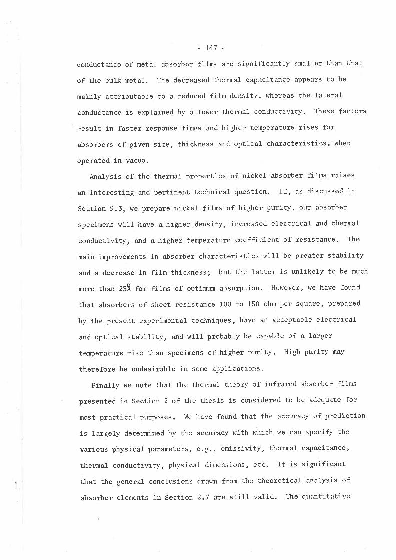
L47 -
conductance of netal absorber filns are significantly smaller tha¡r that
of the bulk netal. The decreased thermal capacitance appeals to be
rnainly attríbutable to a leduced fihn density, whereas the lateral
conductance is explained by a lower thernal conductivity. These factors
result in faster response times and higher tenperature rises for
absorbers of given size, thickness and optical characteristics, when
operated in vacuo.
Analysis of the thernal properties of nickel absorber filns raises
an interesting and pertinent technical question. If, as discussed in
Section 9.5, we plepare nickel filns of higher purity, our absorber
specimens will have a higher density, increased electrical and thermal
conductivity, and a higher temperature coefficient of resistance. The
main improvenents in absorber characteristics rvil1 be greater stability
and a decrease in film thickness; but the latter is wrlikely to be much
nore than ZSR for filns of optinurn absoration. Llowever, we have found
that absorbers of sheet resistance 100 to 150 ohm per squaïe, prepared
by the present experinental techniques, have an acceptable electrical
and optical stability, and will probably be capable of a larger
temperature rise than specinens of higher purity. High purity nay
therefore be undesirable in sone applications.
Finally we note that the thermal theory of infrared absorber filns
presented in Section 2 of the thesis is considered to be adequate for
most practical puryoses. lVe have found that the accuracy of prediction
is largely determined by the accuracy with which we can specify the
various physical pafaneters, ê.g., enissivity, thermal capacitance,
thermal conductivity, physical dinensions, etc. It is significant
that the general conclusions drawn from the theoretical analysis of
absorber elenents in Section 2.7 are still valid. The quantitative

utnurrxBur e^errp€ 01 ropro ur 1.31{1 prmoJ e^?q oM 'osueldlosqe PerejtJur
ro¡[ sluoluorTnbor eqt fq Posoúrr 's1e1eu l€npT^rpuT roJ ITIITT sseu{JTql " sT
eJaql ..ro¡omo¡1 .lueur¡edxe fq perurTJuoJ sel{ sseuì3Trn uITTJ elqrssod lseIT"ltts
Jo acuelJodrur eq¡ 'sseuì.rl{l fllercadso rsuorsueuTp uIITJ uTql pu€ ;(lrnrssnue
.f1rn11cnpuoc Teu6oql 'acuelTcedsf, T€u;eql ''3'e 'sruITJ uTtll uT sTeTIe?'BlIl
Jo sor4odo.rd f¡rceds rnac om qJTTIM r.¡1T¡n fce¡nJJe aql uo luopuedep f1uçeu
sr uoTlcTpeJd Jo fce.rnece eq¡ 'onc€^ ur Pefelado su1r.¡ Ieqrosqe Jo eIIlTl est'I
T€u¡;roql pug osT.r e.rn]e¡edruel eql lcrperd o1 f11n¡ssoccns posn uâoq s"rl sTseql
oql Jo Z uortcêS ur poluesold s;êqfosq€ pe;e4uT Jo '(.roâql 1€uroql eq'L
'Po^oTtlcs
ueeq e^?q lf,o çof d oql Jo suTe or{1 sruIol 1e.reue8 uT l€ql po^oTToq sT 1I
' sJo13elep uor?'"TP?J T€lIIJeql
uT osn roJ raqfosqe crTT€loru luarf,TJJo uB Jo uoTlBJede¡d Jo poqlou unurldo
pu€ sfolau¡e.red leclsfqd perTsop oql eJnpep o1 sEM uoTlualur el€ulTlTn rn0
.uorleJedafd Jo suoTlTpuo3 pue 'elnlcn;ls pue suoTsuolllTp ¡eclsfqd 'flrnTlcnpuoc
IecTrtcoïa eqf pup serlledo¡d osoql ueomloq drqsuollelo"r eql qslTqelse 01 ptIB
. sruTTJ JTITBIou urr.ll Jo sarlredo¡d lectldo PoJ"¡Jur pue Teulfeql 0q1 el?ãrlse^uT
01 sem fpnls sTtlf Jo ulre eql 'sele;tlsqns allerqueu reuflod 01 uo palTsodop
urnno€^ sulTTJ JTITelouI uTtll ur uoTlsTpeI pererJuT Jo uotld'rosç Jo scrs/qd
eql uo fpnls qcI€osal € Jo sllnsor oql pelueseld o^eq ofi srsor{l sTtll uI
SNOISN'ICNO) .
ZT
. sesod*nd e^Tl€r?dtrro3 IoJ el?ÍnJc€ f11ue1cr.5Jns sseleql
-ro^ou se¡1 uoTlorpe.rd IeTlruT er{J 'f11n11cnpuof, T€lufeql pocnpâ;r 01 onp
.q13ue1 l€rlt Jo prTql ouo ÍIeleulTxo;dde Jo üTTJ e JoJ acTlceId ur PesrTso'I
eq plnom lulrJ Ielcru 3uo1 uc I'0 € roJ ¡9¿ eSed) Z ITWL ut uan13
êsrJ oJnle¡edurol pêleTnf,TeJ oqf snqJ. 'suorlclpoJd olBInscB oIoU ur€lqo
olpesnoqI'Ioufeuserpnlsr{f,IeosoJotllJoslTnsare.Ix.flaslenuoc
prm itlcleese.r JeqJosqe ut aprnS TnJosn E oq ol pe^ord e^eq sllnseJ
- 81rï -
_I49_
absorptance in the thinnest possible filn, we need to use higher nelting point
¡netals. In addition, it is clearly desirable that the polyttter substrate be as
thin as practicable. Indeed the substrate is responsible for the najor
contribution to the thernal rise tine.
A predictable relationship has been for.¡nd between the thermal conductivity
and electrical conductivity of nickel and nichrone filns. A sinilar relatíon-
ship has not been observed for gold absorber filns, and it is believed that
this latter result wi11, in general, be characteristic of coarsely crystalline,
lower nelting point metals.
The optical theory of Section 3 predicts a naximu¡n absoïptance (emissivity)
of 0.5 when the sheet resista¡rce of the netal filn is l-89 ohm per square. The
maximurn value of absorptance was confirned by experiment fol all ¡retals studied.
Holever, whereas there was good experimental agreement lvith the predicted
optical-electrical relationship for nickel and nichrorne, thete was no systenatic
relationship for go1d. On the other hand, the absorptance of gold filns is
strongly dependent on thickness. Again we conclude that this is characteristic
of coarsely crystalline netals.
A study of film structure described in Section 10 confirms our predictions,
based on established nucleation and growth phenomena (Section 4), of both the
characteristic structure of a given netal and the influence of structure on
filn properties. In particular, metals having a nelting point higher than
about 1SS9oK will form finely crystalline deposits on ambient temperature
anorphous substrates. These filns, provided they are chenícally inert, tvill
have ¡nore predictable thernal and optical properties than filns of lower rnelting
point netals and will be thinner for the same value of absorptance'
Deposition parameters have a narked influence on the characteristics of
netallic infrared absorbers. In general, the best absorbers are prepared at a
high deposition rate in a pressure of 10-6 torr or better. This observation
- 1s0
applies especially to netals such as nickel, which a1.e prone to oxidation'
The author has concluded that the nost suitable thin filn absorbers are
prepared frorn high nelting point netals. The choice of metals is, unfortunately,
limited (see Sectíon 4,4)i furthermore intrinsic stress may be high in thin
films of these metals, inposing a serious technical difficulty when deposited on
to fragile substrates. The nickel filns prepared in this research project neet
many of the requirements specified for the optinurn infrared al¡sorber. It is
believed that platinurn is the ïnost pronising netal for further investigation'
L3. ACKNOI1ILEDGEMENTS
The author wishes to express his appreciation to his Internal Tutor,
Dr S.G. Tonlin, Ðd External Tutor, Mr N.K. Jones, for their assistance in the
preparation of this thesis. Mr Jones who, as Principal Officer of the autlror|s
Research Group, was responsibl.e for the overall supervision of this task, has
offered nuch valuable advice from his wide experience in the field of infrared
detection.
The author is indebted to Mr M.R. Meharry for many helpful discussions and
constructive crit.icisms, md particularly for assistance with the precision
alignment of optical instrunentation.
Mr J.R. Waller has rendered invaluable technical assistance during the
project. He is responsible for all specimen pTeparations carried out in the
ancillary vacuum coating unit, and nust take the credit for certain specialised
experinents, notably the measurement of temperature coefficient of resistance'
the preparation of nickel specimens for stress analysis, and the investigation
of the electrical properties of gold filns '
Routine preparation of polyrner menbrane substrates was carried out by
Mrs J.M. Jansen.
Finally, the author acknowledges the assistance afforded by other nembers
of the technical staff, and supporting effort provided by the Electronic
Section, Drawing Office and Mechanical Workshop'
-ls1-REFERENCES
)
3
L. Carslaw H.S. and Jaeger J.C.
Mehany, M. R.
Srnith, R. A. , Jones F. E.and Chasnar R.P.
4 , ltJo 1fe , ltl. L.
5. Bleaney, B. I. and Bleaney, B
6. Slater, J.C.
7, Hadni, A
8. Heavens, 0.S
9. Vasicek, A
10. Hadley, L.N. and Dennison, D.M.
11. Hilsun, C
L2, Fuchs, K
13. Sondhiener, E.H.
L4. Chopra, K.L.
frConduction of Heat in Solidsrr (Oxford,Oxford University Press, Second Edition,lese)
Internal W.R.E. Report, L964
rrThe Detection and Measurement of Infra-red Radiationrf(Oxford, Clarendon Press, 1957)
rrHandbook of Military Infrared Technologyt'(Washington, U.S. Governnent PrintingOffice, 1965), Chapter 1
frElectricity and Magnefisnrr(Oxford, Clarendon Press, 1959)
rrQuantum Theory of l¿lolecules and SolidsVol. 3tr. fnsulators, Seniconductors andIvfetals. (New York, McGraw-Hil1, 7967)
rrEssentials of ltlodern Physics Applied tothe Study of the Infraredtr (Oxford,Pergarnon, L967)
t'Optical Properties of Thin Solid Filnsrr(London, Butterworth, 1955)
ilOptics of Thin Filmsrr (Ansterdarn, North-Holland,1960)
trReflection and Transrnission InterferenceFiltersrr Jnl. Opt. Soc. Arn., Vol . 37,No. 6, p.451, June 1947
trlnfrared Absorption of Thin Metal FilmsflJnl. Opt. Soc. Am., Vol. 44, No. 3,p.188, March 1954
rrThe Conductivity of Thin Metallic FilnsAccording to the Electron Theory ofMetalsft Proc. Cambridge Phi1. Soc., Vol.13, p.100, 1938
rrThe Mean Free Path of ElectronsAdvances in Physics, Vol. 1, No.January 1952
in Metalsrr1, P. 1,
rrThin Filn Phenomenarr1e6e)
(N .Y. , McGraw-Hil1,
ilEvaluations of Expressions for theElectrical Resistivity in Thin PlaneSam¡rlesff , Jnl. Appl. Phys., Vol . 36, p.3947,1965
15. Soffer, S
ts2 -
16. Rhodin, T.N., and Walton, D
17. Hirth, J.P. and Pound, G.M.
18. Lewis, B. and Canpbell, D.S.
19. Lewis, B
20. Neugebauer, C.A.
2L. Pashley, D.W.
22. Pashley, D.W., et al
25. Chopra, K.L. G Randlett, M.R.
24. Komnilc, Yu. F
25. Kosevich, V.M. et al
26. Levinstein, H
27. Sennett, R.S. õ Scott, G.D.
rrThe Use of Thin Filns in PhysicalInvestigationsrr, J.C. Anderson, Ed.(N.Y., Acadenic Press, 1966) p.187
rrHeterogeneous Nucleation on Substtatesrl(In rrCondensation and Evaporationrr,Oxford, Pergamon, 1965)
rrNucleation and Initial Growth Behaviourof Thin Filn Depositsrt, Jnl. Vacuum Sci.and Tech., Vol. 4, lrlo. 5, p.209, 1967.
ilBond Energy Formulations of HeterogeneousNucleation Theorytr, Thin Solid Films,Vol. 1, p.85, 1967
rrCondensation, Nucleation and Growth ofThin Filnsrt, in 'rHandbook of Thin Fil¡nTechnologyrr, L.I. It{aissel and R. Glang(Eds), (N.Y., li{cGraw-Hi11, 1970)
ItThe Nucleation, Growth, Sttucture andEpitaxy of Thin Surface Filmsrr, Adv. inPhysics, Vol. 14, No. 55, P.327, JUIY1965
rrThe Growth and Structure of Gold andSilver Deposits Forned by EvaporationInside an Electron Microscoperr, Phi1. Mag.,Vo1. 10, No. 103, p.L27, July 1964
ilInfluence of Deposition Parameters of theCoalescence Stage of Growth of Metal Fillnsrr,Jnl. Appl. Phys., Vo1. 39, No. 5, p.L874,February 1968
ItCharacteristic Condensation Temperaturesof Thin Filmsrr, Soviet Phys - Solid State,Vol.6, I'lo. 10, p.2309, April 1965
ilThe Form of Metallic Condensate Particlesin the Initial Stages of Growthrr, SovietPhys - Solid State, Vol. 6, No. LL, p.2591May 1965
'rGrowth and Structure of Thin Metallic FilnuJn1. Appl. Phys., Vol.20, p.306, April1949
rrThe Structure of Evaporated Metal Filnsand Their Optical Propertiesrr, Jnl. Opt.Soc. Am., VoI. 40, No. 4, P.203, Ãpri1 1950
ItElectrical Resistivity of Thin SingleCrystal Gold Filmsr', Jnl. Appl. Phys,,
28. Chopra, K.L. et al

153 -
29. Belser, R. B.
30. Chopra, K.L
31. Herman, D.S. and Nrodin, T.N.
32, HiLl, R.M.
Vol. 34, No. 6, p.1699, June 1963
rrElectrical Resistance of Thi,n MetalFilms,Before and After Artificial Agingby Heatingtr, Jnl. Appl. Phys., Vol. 28,No. 1, p.109, January L957
rrlnfluence of Electric Field on theGrowth of Thin Metal Filmsrt, JnI. Appl.Pltys . , Vo 1 . 37, No . 6, p. 2249 , It{ay 1966
'rElectrical Conduction Between MetallicMicroparticlesil Jn1. Appl. Phys., Vol.37,No. 4, p,1594, March l-966
rrElectrical Conduction in DiscontinuousMetal Filnsrr Contemp. Phys., Vol. 10,No. 3, p,22I, 1969
Mullard Res. Lab. Rep. 466, 1963
rrStructural Aspects of the Magnetizationin Ultrathin Fenomagnetic Filnsrr Z.Angew Phys . , Vol. 1-4, No . 4, p.LB2,April L962.
33.
34.
Fleet, S.G.
Neugebauer, C.A.
35. Glang, R
56. Hol1and, L
37. UnvaLa, B.A. and Grigson, C.W.B
38. Gillespie, F.C.
59. Hilr, P.J.
40. Tolansky, S
41. Schartz, B. andSchwartz, N. (Editors)
'tVacuum Evaporationrr Clì.of Thin Film TechnologyHil1,1970)
1o(N.Y
f Handbook., McGraw-
42. BennettBennettAshley,
, H.E.,, J.M.E.J.
rrVacuum Deposition of Thin Filmsrr (London,Chapnan and IIal1, 1956)
rrPrecision Electron Bombardment Ftrrnacefor Lligh Purity Evaporation of SiliconrrProc. Fifth Electron Bean Synposiurn,Boston, lvlass., P.168 , 1963
rrVacuurn Evaporation Experiences with aRing-type Electron Bearn Gr¡nrr Vacuum, Vol.22, No.7, p.255, JuIy 1972
W.R.E. Technical Report (unpublished)
rrMultiple-Bean Interferonetry of StrrfaceFilmsr' (London, Oxford University Press,1948)
'rOptinization of the Tolansky TechniqueFor Thin Filn Thickness N{easurementrr,in Measurernent Techniques for Thin Filns(N.Y., Electrochenical Society, L967)
rrlnfrared Reflecta¡ce of EvaporatedAluniniun Filmsil Jnl. Optical Soc. Am.,Vol. 52, No. 11, p.L245, Novenbe-r L962
and

45. Liddiard, K.C.
44. ALderson, R.H. and Ashworth, F.
45, Degenhart, H.J. and Pratt, I.H.
46. Siddall, G, and Probyn, B.A.
47. lVied, 0.J. and Berner, W.E.
48. Caruso, S.V. and Dettaye, R.F.
49. Ziman J. M.
50. Neugebauer, C.A. and Webb, M.B.
51. Hoffnan, R.W.
52. Carnpbell, D.S.
55. Klokholm, E. and Berry, B.S.
54. Kay, D.H. (Editor)
55. Morris, J.E.
154 -trResearch Studies on Metal Film InfraredBolometer DetectorsrtW.R.E. Tcchnical Notc, in prcparation
tt!4suum-Deposited Filns of Nickel Chromiu¡nAlloyil Br. Jnl. Appl. Phys., Vol. 8,p.208, May 1957
ItThickness and Conposition of Nickel-Chroniun Fil¡nsr? Trans. 10th Nat. Vac.Synp. , p. 480 (N.Y. , Maclvlillan , 1963)
rrVacuum-Deposited Metal Filn ResistorsrrBr.Jnl. Appl. Phys., Vol. L2, p.668,Decenber, 1961
rrThe Dependence of the ElectricalCharacteristics of Ni-Cr Thin Films onEvaporation Parametersrr Trans. ThirdInt. Vac. Congress, Vol. 2, Pt. 1, p.59,1965
rfProperties of Vacuum-Deposited Thin-Filn Nichrome Resistorsrr Proc. SecondITIASA Microelectronics Synp. , p.101,1966.
rrElectrons and PhononsrrPress, 1960)
(Oxford, Clarendon
frElectrical Conduction Mechanisn inUltrathin, Evaporated Metal Filnsrr Jnl.Appl. Phys., Vol. 33, No. t, p.74,January t962
I'Mechanical Properties of Thin CondensedFilmsil in Physics of Thin Filns, Vol. 3,(N. Y. , Acadernic, 1963)
rrMechanical Properties of Thin FilnsrtRef.35, Ch.12
frlntrinsic Stress in Evaporated MetalFilnsrr Jnl. Electrochem. Soc., Vol. 115,No. 8, p.823, August 1968
rrTechniques for Electron Microscopyrr(Oxford, Blackwell , 2nd Ed., 1965)
ttResistance Changes of Discontinuous GoldFilns in Airrf , Thin Solid Fil¡ns, VoI. 5,p,539, L970

-155-
56. Bricknell, R.W. et al
57, Neugebauer, C.A.
58. Reale, C.
59. Meha:r)r, M.R. 6 Brown, D.ll.
60. Abrosinov, V.M. et al
ilThe Structure of Vacuun Condensed Ni-Cr Filnsrr Microelectronics and Rel.,Vol.3, p.61¡ 1964.
rfSaturation Magnetízatíon of NiclelFilns of Thickness Less than L00RrtPhys. Rev,, Vol. 116, No.6, p.744L, LSDecember, 1959.
ffElectrical Properties of VacuumDeposited Nickel FiLns'r, Phys. Lettors,Vol. 244, No. 3, p.145, 50 January,1967,
rrA Scanning Radioneter for MeasuringThernal Spread in Thin I',lenbranesil,lli. R. E. Internal Technical Report .
"Investigation of the thernal Conductivityof Thin Metallic Filnsrr, Soviet Phys.Solid State, Vol. 11, No.2, p.427,August, 1969._t
I
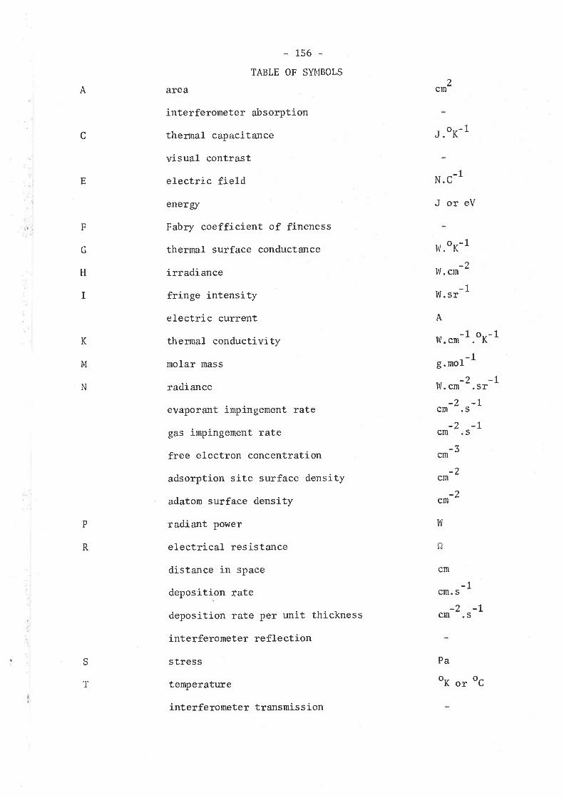
A
c
E
-156-TABLE OF SYIvIBOLS
area
interferoneter abs orption
thernal capacitance
visual contrast
electric field
energ:r
Fabry coefficient of fineness
thermal surface conductance
irradiance
fringe intensity
electric current
thermal conductivity
molar ¡nass
radiance
evaporant impingement rate
gas inpingenent rate
free electron concentration
adsorption site surface density
adaton surface density
radiant poüJer
electrical resistance
distance in space
deposition rate
deposition rate per unit thickness
interferometer reflection
stress
temperature
interferometer transmiss ion
2cm
J.oK-1
N.C -T
JoreV
_')lv. cn
_1W.sr ^
A
W. cm-1.oK-1
F
G
H
I
lv. or-1
K
M
N
_1g.nol t
_)W.cn -
-2cm .s
-1.sr-1
-1.-2cm
-3cm
^-1cn
-2cn
S
hr
-1cn. s
-2 -1cm S
Pa
oK ot oc
a)
P
R
cn
S
T

VV
hr
157 -
potential
radiant emittance
fringe half width
Youngrs Modulus
as prefix, incrernental values of above
physical quantities
absorber radius
fringe displacenent
fringe separation
specifÍc heat
wave velocity in free space
distance or thickness
wedge spacing
electronic charge
frequency
collision frequency
Plankrs constant
height
Boltzmann constarit
absorption index
length
electronic nass
refractive index
fringe order
pressure
specularity paraneter
radius
Y
IV-2.cm
R
Pa
cln
R
R
- -1 o.--1J.g . K
universal constant
cm
cm
universal constant
Hz
-1s
trniversal constant
cn
universal constant
universal constant
torr
a
b
c
d
e
f
oè
h
k
L
n
n
cn
P
cmr
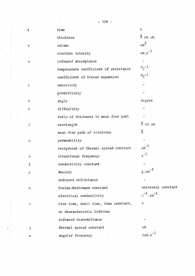
st
cmv
0
o
T
-158-
tine
thickness
volume
electron velocity
infrared absorptance
tenperature coefficient of resistance
coefficient of linear expansion
emissivity
perrnittÍ.vity
angle
diffusivity
ratio of thickness to nean free path
wavelength
nean free path of electrons
permeability
reciprocal of thernal spread constant
vibrational frequency
conductivity constant
density
infrared reflectance
Stefan-Bo ltzmann constant
electrical conductivity
rise tine, dwell time, tine constant,
or characteristic lifetime
infra¡ed transmittance
thernal spread constant
angular frequency
R or um
J
1cm. s
oc- 1
C
oc-1
degree
RorutR
-1um
0
K
À
u
1V
E
p
S
-3g. cn
universal constant
l¿-1 -1.cm
S
um
rad. s
X
(¡-1

Notes
-L59-
(a) Symbols conforn to British Standards, except in radionetry
where the symbols are based on widely accepted notation. This
has caused dupl_ication in some instances, a situation which is
aggravated by the several disciplines demanded in the project.
Care has been taken to avoid duplication in the sane sections
of the thesis.
(b) lVide use is nade of subscripting to distinguish between various
values of the sane physical quantity, and to avoid confusion
between different physical quantities.
(c) The Greek symbol A is r¡sed as a prefix to denote increnental
values of the physical quantities in the Symbol Table.
(d) SI units are used throughout, except that length is expressed
in cn in acçord with connon practice in infrared technology.
Consequently, mass is given it g, density in g."t-S.