Transfer printing of graphene strip from the graphene grown on copper wires
Upload
independentCategory
view
2download
0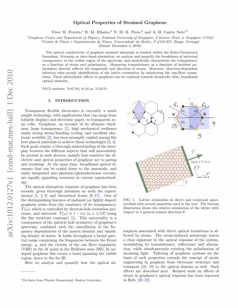
Optical Properties of Strained Graphene
Vitor M. Pereira,1 R. M. Ribeiro,2 N. M. R. Peres,2 and A. H. Castro Neto∗1
1Graphene Centre and Department of Physics, National University of Singapore, 2 Science Drive 3, Singapore 1175422Centro de Fısica e Departamento de Fısica, Universidade do Minho, P-4710-057, Braga, Portugal
(Dated: December 2, 2010)
The optical conductivity of graphene strained uniaxially is studied within the Kubo-Greenwoodformalism. Focusing on inter-band absorption, we analyze and quantify the breakdown of universaltransparency in the visible region of the spectrum, and analytically characterize the transparencyas a function of strain and polarization. Measuring transmittance as a function of incident po-larization directly reflects the magnitude and direction of strain. Moreover, direction-dependentselection rules permit identification of the lattice orientation by monitoring the van-Hove transi-tions. These photoelastic effects in graphene can be explored towards atomically thin, broadbandoptical elements.
PACS numbers: 78.67.Wj, 81.05.ue, 73.22.Pr
I. INTRODUCTION
Transparent flexible electronics is currently a muchsought technology, with applications that can range fromfoldable displays and electronic paper, to transparent so-lar cells. Graphene, on account of its ultimate thick-ness, large transparency [1], high mechanical resilienceunder strong stress/bending cycling, and excellent elec-tronic mobility [2], has been promptly ranked among thebest placed materials to achieve those technologies [3, 4].Such goals require a thorough understanding of the inter-play between the different aspects that will unavoidablybe present in such devices, namely how sensitive the di-electric and optical properties of graphene are to gatingand straining. At the same time, broadband optical el-ements that can be scaled down to the nanoscale, andeasily integrated into photonic/photoelectronic circuits,are equally appealing scenarios in current nanotechnol-ogy.
The optical absorption response of graphene has beenrecently given thorough attention on both the experi-mental [1, 5–8] and theoretical fronts [9–17]. One ofthe distinguishing features of undoped (or lightly doped)graphene arises from the constancy of its transparency,T (ω), which is controlled by electron-hole excitation pro-cesses, and universal: T (ω) ≈ 1 − πα (α ' 1/137 beingthe fine structure constant) [1]. This universality is aconsequence of the particle hole symmetry of graphene’sspectrum, combined with the cancellation of the fre-quency dependencies of the matrix element and vanish-ing density of states. It holds throughout a broad spec-tral range comprising the frequencies between the Fermienergy, µ, and the vicinity of the van Hove singularity(VHS) at the M point in the Brillouin zone (BZ). In un-doped graphene this covers a band spanning the visibleregion, down to the far IR.
Here we analyze and quantify how the optical ab-
∗On leave from Physics Department, Boston University.
FIG. 1: Lattice orientation in direct and reciprocal space,overlaid with several quantities used in the text. The bottomillustration shows the relative orientation of the lattice withrespect to a general tension direction θ.
sorption associated with direct optical transitions is af-fected by strain. The strain-induced anisotropy leavesa clear signature in the optical response of the system,modulating its transmittance, reflectance and absorp-tion, while simultaneously rotating the polarization ofincoming light. Tailoring of graphene systems on thebasis of such properties extends the concept of strainengineering in graphene from electronic structure andtransport [18, 19] to the optical domain as well. Sucheffects are described next. Related work on effects ofstrain in graphene’s optical response has been reportedin Refs. [20–22].
arX
iv:1
012.
0127
v1 [
cond
-mat
.mes
-hal
l] 1
Dec
201
0

2
II. STRAIN-INDUCED ANISOTROPY
We concentrate on uniform uniaxial deformations offree graphene, which provide the highest degree ofanisotropy for given amount of strain, ε. Within a tight-binding approximation for the π-band subsystem, strainimpacts electronic motion via the modification of theSlater-Koster parameters ti ≡ t(δi) in the Hamiltonian
H =∑R,δ
t(δ) a†RbR+δ + H. c. . (1)
Here R denotes a position in the Bravais lattice; δ1,2,3connects site R to its neighbors; a(R) and b(R) arethe field operators in sublattices A and B. In what fol-lows, we characterize the interplay between strain andelectronic structure in the same framework describedin detail in ref. 23. In summary, this entails the as-sumption that hopping amplitudes vary with distance ast(r) ' te−λ(r−a), with t ≈ 2.7 eV, a = 1.42 A, λa ≈ 3− 4[21, 23], and we disregard bond bending effects, sincethey are not significant in this effective description [24].Bond deformations are uniform and given to linear or-der in terms of the strain tensor εij : δ = (1 + ε) · δ0.This approximation was shown to describe with goodaccuracy both the threshold deformation for the Lif-shitz and metal-insulator transition at large deformations[23, 25, 26], and the behavior of ti(δ) when compared toab-initio calculations [24]. Since the hexagonal lattice iselastically isotropic, εij can be fully parametrized by theamount of uniaxial strain, ε, its direction θ with respectto a zig-zag (ZZ) direction, and Poisson’s ratio, ν ≈ 0.16[23]. Our Cartesian directions are such that a ZZ edgecoincides with the x axis (fig. 1). Tension along θ = 0[ZZ] and θ = π/2 [armchair (AA)] defines representativedirections that will be recalled frequently. We shall dis-regard the strain-induced modification of the reciprocallattice, as it is not relevant for the optical absorption.Since here we are not interested in large deformations,we further approximate ti ≡ t(δi) ≈ t− tλ(δi − a).
The low energy Hamiltonian appropriate for opticalprocesses below the UV can be derived conventionally[16], by expanding (1) around the shifted Dirac points:k = kD+q (q � kD). For arbitrary ti the nonequivalentDirac points lie at kD,ζ = ζ(A − B, A + B), with A =1√3a
cos−1t21−t
22−t
23
2t2t3, B = 1
3a cos−1t23−t
21−t
22
2t1t2, and ζ = ±1
is the valley index, labeling the two nonequivalent Diracpoints. In their vicinity, the electronic dispersion is givenby
E2q '
9
4q2ya
2t22 +3√
3
2qxqya
2(t23 − t21)
+3
4q2xa
2(2t21 − t22 + 2t23) +O(q3). (2)
The Fermi surface is consequently an ellipse, with prin-cipal axes that will be rotated with respect to Oxy inthe general situation. eq. (2) can be cast compactly as
E2q = ~2v2F×q.η2.q, where ~vF ≡ 3ta/2. Diagonalization
of η2 yields the principal velocities v2± = v2F η2±, with
η2± =t21 + t22 + t23
3t2
± 2
3t2
√t41 + t42 + t43 − t21t22 − t22t23 − t21t23, (3)
and the principal directions:
tanϕ± =t23 − t21√
3(η2±t2 − t22)
. (4)
These directions define the slow/longitudinal (−, l) andfast/transverse (+, t) directions of strained graphene, in-sofar as the direction-dependent Fermi velocity in theelliptical Fermi surface is smallest along the one, andlargest along the other. In the principal coordinate sys-tem, the effective Hamiltonian of valley ζ = ± reads
Hζ ' ζvF τ1ηlpl + vF τ2ηtpt, (5)
where τ1,2 are Pauli matrices acting on the (A,B) sub-lattice space. Coupling to a light wave described bythe physical vector potential A(t) = A0 exp(−iωt) isachieved by the minimal substitution p → p + eA ineq. (5). The frequency-dependent conductivity is ex-tracted from the linear response to A0.
For future reference, the anisotropy parameters will beexpressed directly in terms of the longitudinal deforma-tion ε, to first order. For general tension along θ withrespect to Ox we have
ηt ' 1 + aλνε, ηl ' 1− aλε, (6a)
δkD,ζ ' ζλε1 + ν
2(cos 2θ,− sin 2θ), (6b)
tanϕl '[1− aλε1 + ν
8(1 + 2 cos 4θ)
]tan θ, (6c)
tanϕt '[1 + aλε
1 + σ
8(1 + 2 cos 4θ)
]tan(θ +
π
2
).
(6d)
As intuition dictates, the slow/longitudinal axis is co-incident with the tension axis (ϕ ≈ θ). From (5) thestrain-induced correction to the density of states (DOS)in the vicinity of the Dirac points follows immediately:ρ(E) ' ρiso(E)/(ηlηy), where the isotropic DOS readsρiso(E) = 2|E|/(π~2v2F ). Notice that, even though theeffective longitudinal (transverse) velocity increases (de-creases), the net effect in the DOS is always a slope en-hancement, because ηlηt ≈ 1 − aλ(1 − ν)ε < 1. Thismeans that strain modifies the Fermi energy and/or elec-tron density.

3
III. CONDUCTIVITY OF STRAINEDGRAPHENE
Kubo’s form of the frequency dependent conductivityreads
σαβ(ω) =igsq
2
Aω
∑kλλ′
vkλλ′
α vkλ′λ
β (nkλ − nkλ′)
~ω − (εk,λ′ − εk,λ) + i0+, (7)
where gs = 2 is the spin degeneracy, A the total area,λ, λ′ = ±, and vkλλ
′
α ≡ 〈k, λ|vα|k, λ′〉 are the matrixelements of the velocity operator vα = i~−1[H,xα] inthe momentum eigenbasis. For the general tight-bindingHamiltonian (1), these matrix elements read explicitly
〈k, λ|v|k′, λ′〉 = −λ~δk,k′δλλ′
∑α
tαδα sin [k.nα − θk]
− iλ
~δk,k′ (1− δλλ′)
∑α
tαδα cos [k.nα − θk] , (8)
with θk = arg[∑
i ti exp(ik.ni)]. Contributions with
λ = λ′ are associated with intra-band transitions, andλ 6= λ′ with inter -band, direct transitions. In this formthe conductivity can be directly calculated at the tight-binding level. In order to proceed fully analytically wework in the Dirac approximation (5), and consider a cleansystem at zero temperature, thus retaining only the inter-band contribution. In the principal coordinate system de-fined by the slow/longitudinal and fast/transverse axesthe relevant matrix elements become:
|vk,λ,−λl |2 ≈ v2F η2l sin2 θkD, (9a)
|vk,λ,−λt |2 ≈ v2F η2t cos2 θkD, (9b)
vk,λ,−λl vk,−λ,λt ≈ ζ v2Fηlηt2 sin(2θkD
). (9c)
The anisotropy is explicitly encoded both in the param-eters η±, and in the phase θkD
.From here and eq. (7) it is straightforward to obtain
the frequency dependent conductivity σαβ = σ′αβ + iσ′′αβ .Its real part reads
σ′ll(ω) ' ηlηt× σ0 ×
[f(−~ω
2 − µ)− f
(~ω2 − µ
)](10)
for the longitudinal conductivity, and σ′tt(ω) =(ηt/ηl)
2 σ′ll(ω) for the transverse component. Theisotropic (and universal) value is σ0 = e2/(4~), and f(x)represents the Fermi-Dirac occupation function. Theimaginary part, σ′′(ω), reads
σ′′ll(ω) ' ηlηt× σ0
π× log
∣∣∣∣2|µ| − ω2|µ|+ ω
∣∣∣∣ (11)
when T = 0, and σ′′tt(ω) = (ηt/ηl)2 σ′′ll. The off-diagonal
components σlt are zero, as one expects from symmetryand the absence of magnetic fields. This result showsthat σ′ii(ω) is still constant within the region of validity
of the Dirac approximation, and for 2µ . ~ω � T , be-ing only renormalized by the anisotropy factors η±. Thedegree of anisotropy is controlled by ηl/ηt, which is a
sensible result because σii(ω) ∝ |vk,λ,−λi |2, and the ratioreflects the quotient between the Fermi velocities alongthe principal strain directions. From Eqs. (10) and (11),and recalling the expressions in eq. (6a), we can expressthe strain induced corrections to the full isotropic con-ductivity, σ(ω) = σ′(ω) + iσ′′(ω), in linear order in thedeformation as
σll,tt(ω) ' σiso(ω)×(1∓ 2|δkD|a
), (12)
where σiso(ω) represents the full frequency-dependentconductivity in the absence of strain. For example, ten-sion along ZZ (θ = 0) yields a decrease in σxx, and anincrease of the same magnitude for σyy. Substitutionof the material parameters applicable to free-standinggraphene in (12) and (6b) yields an anisotropy factor(σt−σl)/σiso = 4|δkD|a ∼ 8ε. This is sufficiently markedto be detectable by conventional optical means, like ab-sorption in the visible or IR, which we discuss below.
IV. AB-INITIO OPTICAL CONDUCTIVITY
Given the approximations used, it is legitimate to ques-tion the validity of the analytical corrections written ineq. (12). To that end, we have extracted the opticalconductivity of uniaxially strained graphene from first-principles as well. Density Functional Theory (DFT) cal-culations were performed with the ab-initio spin-densityfunctional code aimpro [27]. We used the GGA in thescheme of Perdew, Burke, and Ernzerhof [28]. Core stateswere accounted for by dual-space separable pseudopoten-tials [29]. The valence states are expanded over a set of s,p, and d-like localized, atom-centered Gaussian functions.The BZ was sampled according to the scheme proposedby Monkhorst-Pack [30]. We used a convergence-testedgrid of 20× 20××1 points for the self-consistent calcu-lations. In equilibrium we obtained the optimized latticeparameter a = 1.42 A.
Uniaxial strain was applied with relaxation as de-scribed earlier in Ref. 24. For each strained configura-tion we extracted the dielectric function within the long-wavelength dipole approximation [31], and from it theoptical conductivity. The results for σ′xx(ω) and σ′yy(ω)so obtained are shown in fig. 2, for representative uniaxialstrains applied along ZZ (θ = 0) and AA (θ = π/2).
The main panel of fig. 2(a) shows the renormalizationof the real part of σxx, which corresponds to σll for ZZand σtt for AA. It is clear that for visible and IR fre-quencies the conductivity remains roughly constant inω, but its magnitude depends on the amount of strain.The strain dependence is shown in detail in the inset,at ω = 1 eV. The perfect linearity in ε of the ab-initioresults up to at least ε ≈ 10% shows that the analyt-ical result of eq. (12) is indeed quite dependable for a
4
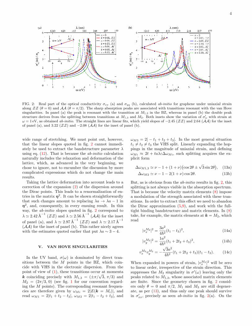
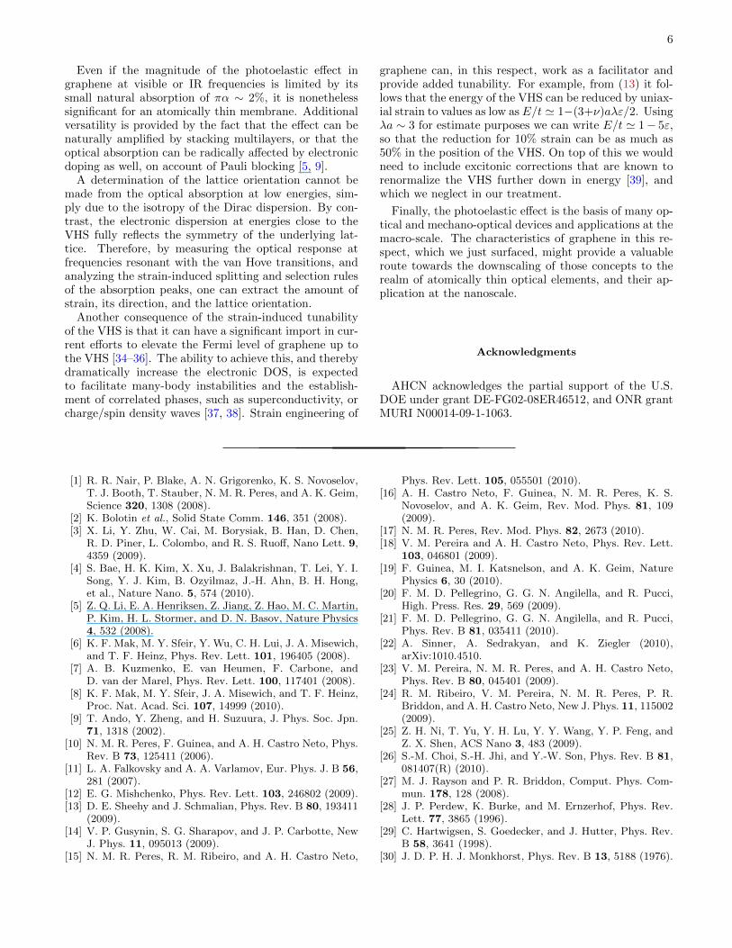
FIG. 2: Real part of the optical conductivity σxx (a) and σyy (b), calculated ab-initio for graphene under uniaxial strainalong ZZ (θ = 0) and AA (θ = π/2). The sharp absorption peaks are associated with transitions resonant with the van Hovesingularities. In panel (a) the peak is resonant with the transition at M1,3 in the BZ, whereas in panel (b) the double peakstructure derives from the splitting between transitions at M1,3 and M2. Both insets show the variation of σ′ii with strain atω = 1 eV, as obtained ab-initio. The straight lines are linear fits, which yield slopes of −2.45 (ZZ) and 2.64 (AA) for the insetof panel (a), and 3.22 (ZZ) and −2.08 (AA) for the inset of panel (b).
wide range of stretching. We must point out, however,that the linear slopes quoted in fig. 2 cannot immedi-ately be used to extract the bandstructure parameter λusing eq. (12). That is because the ab-initio calculationnaturally includes the relaxation and deformation of thelattice, which, as advanced in the very beginning, wechose to ignore, not to encumber the discussion by morecomplicated expressions which do not change the mainresults.
Taking the lattice deformation into account leads to acorrection of the expansion (2) of the dispersion aroundthe Dirac points. This leads to a renormalization of en-tries in the matrix η2. It can be shown straightforwardlythat such changes amount to replacing λa → λa − 1 inη2, and, consequently, in every ensuing result. In thisway, the ab-initio slopes quoted in fig. 2 correspond to
λ ' 2.42 A−1
(ZZ) and λ ' 2.56 A−1
(AA) for the inset
of panel (a), and λ ' 2.97 A−1
(ZZ) and λ ' 2.17 A−1
(AA) for the inset of panel (b). This rather nicely agreeswith the estimates quoted earlier that put λa ∼ 3− 4.
V. VAN HOVE SINGULARITIES
In the UV band, σ(ω) is dominated by direct tran-sitions between the M points in the BZ, which coin-cide with VHS in the electronic dispersion. From thepoint of view of (1), these transitions occur at momenta
k coinciding precisely with M1,3 = (±π/√
3, π/3) andM2 = (2π/3, 0) (see fig. 1 for our convention regard-ing the M points). The corresponding resonant frequen-cies are therefore given by ωMi = 2|E(k = Mi)|, andread ωM1 = 2|t1 + t2 − t3|, ωM2 = 2|t1 − t2 + t3|, and
ωM3 = 2| − t1 + t2 + t3|. In the most general situationt1 6= t2 6= t3 the VHS split. Linearly expanding the hop-pings in the magnitude of uniaxial strain, and definingωMi ≈ 2t + taλε∆ωMi, such splitting acquires the ex-plicit form
∆ωM1,3 ' ν − 1 + (1 + ν)(cos 2θ ±
√3 sin 2θ
), (13a)
∆ωM2 ' ν − 1− 2(1 + ν) cos 2θ. (13b)
But, as is obvious from the ab-initio results in fig. 2, thissplitting is not always visible in the absorption spectrum.That is because the velocity matrix elements (8) imposea modulation of the strength associated with these tran-sitions. In order to extract this effect we need to abandonthe Dirac approximation (5,9), and work with the full-tight binding bandstructure and matrix elements. In (8)take, for example, the matrix elements at k = M2, whichread
|vM2x |2 =
3a2
4~2(t1 − t3)2, (14a)
|vM2y |2 =
1a2
4~2(t1 + 2t2 + t3)2, (14b)
vM2x vM2
y = −√
3a2
4~2(t1 + 2t2 + t3)(t1 − t3). (14c)
When expanded in powers of strain, |vM2x |2 will be zero
to linear order, irrespective of the strain direction. Thissuppresses the M2 singularity in σ′(ω) leaving only thepeaks related to M1,3, whose associated matrix elementsare finite. Since the geometry chosen in fig. 2 consid-ers only θ = 0 and π/2, M1 and M3 are still degener-ate, as per (13), and thus only one peak should survivein σ′xx, precisely as seen ab-initio in fig. 2(a). On the

5
FIG. 3: Illustration of the behavior of the transmittance asa function of incident polarization measured in the labora-tory frame. According to (16), the phase shift θ defines thedirection of strain, and the amplitude its magnitude.
other hand, there is no such selection rule arising fromthe velocity matrix elements when computing σ′yy, whichallows the splitting between M2 and M1,3 to be observed,as fig. 2(b) clearly demonstrates. Eqs. (13) also explainwhy in fig. 2(a) the strain-induced shift of the peak isless pronounced for tension along ZZ (θ = 0), than AA(θ = π/2): ∆ωM1(ZZ) = ν ∆ωM1(AA). And similarly,Eqs. (14) account for the different relative intensity ofthe peaks associated with M2 and M1,3 in fig. 2(b).
It is important to stress here that these results are nottied to a particular coordinate system. We can easily ex-press Eqs. (14) in any coordinate system, rotated by ϕwith respect to Oxy, and conclude that the longitudinalmatrix element |vMi
x′ |2 always vanishes when ϕ coincides
with a ZZ direction. For example, |vM2
x′ |2 vanishes for
ϕ = 0, |vM3
x′ |2 vanishes for ϕ = π/3, and |vM1
x′ |2 vanishesfor ϕ = 2π/3. Suppression of a van Hove peak in the lon-gitudinal conductivity therefore singles out one of the ZZdirections of the lattice. This is consistent and explainsthe numerical calculations of Ref. 21, and has an im-portant consequence: by monitoring the splitting in theabsorption peaks associated with VHS, and by inspectingthe selection rule just described, one can measure simul-taneously: the magnitude of strain, its direction, and thedirection of the underlying lattice with respect to the labo-ratory coordinate system. This provides an optical meansto perform the same measurements that have been madeby exploring the splitting of the G peak in the Ramanspectrum of strained graphene [32, 33].
VI. TRANSPARENCY AND DICHROISM
The asymmetry (12) in the conductivity tensor will re-sult in a certain degree of dichroism, as the absorbanceof linearly polarized light will depend on the polarizationdirection with respect to the slow/fast axes. Treatinggraphene as a 2D conducting sheet, and solving the as-sociated Fresnel equations, we can extract the degree ofpolarization rotation for normal incidence on graphenein vacuum. In the visible and IR where eq. (12) stands
that would be
tanφTtanφI
=2 + cµ0σll2 + cµ0σtt
≈ 1− 4|δkD|acµ0σ0
2 + cµ0σ0, (15)
where φT,I are the transmitted and incident polarizationsmeasured with respect to the slow/longitudinal axis, andcµ0σ0 = πα ≈ 0.02. Likewise, the transmittance forlinear polarization becomes
T ≈ 1− πα[1− 2|δkD|a cos 2φI
](16)
An important consequence of this periodic modulation isthat it allows a direct determination of both the strain di-rection and its magnitude, as follows. In some laboratorycoordinates (16) is transformed by making φI → φI−ϕl.The amplitude of T as a function of polarization direc-tion determines the amount of strain, while the phaseshift ϕl fixes the direction. This is illustrated in fig. 3.The corrections to both polarization and transmittanceare weighted by πα, and will be necessarily small. But,one the one hand, the modulation amplitude is roughly∼ 8επα (0.16ε) and transmittance can be routinely mea-sured within 0.1% of precision. On the other hand, thetransmittance of multilayer graphene is, to a great ex-tent, cumulative [1, 7]. This implies that the same re-sults apply for multilayer graphene, provided one replacesπα → Nπα in (16), where N accounts for the numberof graphene layers. The effect is thus naturally enhancedin multilayers, as it is in the vicinity of the VHS (or anyresonance, for that matter). Another interesting appli-cation is that, if strain can be controlled with precision,an expression like (16) allows, by means of a simple op-tical experiment, the measurement of the bandstructureparameter λ = d log t/dr, whose knowledge is crucial forthe characterization of all strain-induced effects on thebandstructure.
VII. DISCUSSION
The photoelastic effect in undoped graphene has beenquantified, and shown to possess features that might beappealing in the development of atomically thin opticalelements. One of such characteristics is the frequencyindependent response in a very large frequency range,which remains valid when the system is anisotropicallystrained. This constancy and predictability is a rele-vant feature for broadband applications. The degree ofanisotropy induced by strain is determined by how muchthe Dirac point is displaced from its position at K/K ′
in the BZ: |δkD| (6b). This opens several possibilities,such as: monitoring optical absorption as a function ofstrain to characterize the band parameters of graphene;or monitoring the transmittance as a function of incidentpolarization in order to measure the magnitude and di-rection of strain in graphene devices. This last examplecould find applications in completely passive, transpar-ent, strain sensors.
6
Even if the magnitude of the photoelastic effect ingraphene at visible or IR frequencies is limited by itssmall natural absorption of πα ∼ 2%, it is nonethelesssignificant for an atomically thin membrane. Additionalversatility is provided by the fact that the effect can benaturally amplified by stacking multilayers, or that theoptical absorption can be radically affected by electronicdoping as well, on account of Pauli blocking [5, 9].
A determination of the lattice orientation cannot bemade from the optical absorption at low energies, sim-ply due to the isotropy of the Dirac dispersion. By con-trast, the electronic dispersion at energies close to theVHS fully reflects the symmetry of the underlying lat-tice. Therefore, by measuring the optical response atfrequencies resonant with the van Hove transitions, andanalyzing the strain-induced splitting and selection rulesof the absorption peaks, one can extract the amount ofstrain, its direction, and the lattice orientation.
Another consequence of the strain-induced tunabilityof the VHS is that it can have a significant import in cur-rent efforts to elevate the Fermi level of graphene up tothe VHS [34–36]. The ability to achieve this, and therebydramatically increase the electronic DOS, is expectedto facilitate many-body instabilities and the establish-ment of correlated phases, such as superconductivity, orcharge/spin density waves [37, 38]. Strain engineering of
graphene can, in this respect, work as a facilitator andprovide added tunability. For example, from (13) it fol-lows that the energy of the VHS can be reduced by uniax-ial strain to values as low as E/t ' 1−(3+ν)aλε/2. Usingλa ∼ 3 for estimate purposes we can write E/t ' 1− 5ε,so that the reduction for 10% strain can be as much as50% in the position of the VHS. On top of this we wouldneed to include excitonic corrections that are known torenormalize the VHS further down in energy [39], andwhich we neglect in our treatment.
Finally, the photoelastic effect is the basis of many op-tical and mechano-optical devices and applications at themacro-scale. The characteristics of graphene in this re-spect, which we just surfaced, might provide a valuableroute towards the downscaling of those concepts to therealm of atomically thin optical elements, and their ap-plication at the nanoscale.
Acknowledgments
AHCN acknowledges the partial support of the U.S.DOE under grant DE-FG02-08ER46512, and ONR grantMURI N00014-09-1-1063.
[1] R. R. Nair, P. Blake, A. N. Grigorenko, K. S. Novoselov,T. J. Booth, T. Stauber, N. M. R. Peres, and A. K. Geim,Science 320, 1308 (2008).
[2] K. Bolotin et al., Solid State Comm. 146, 351 (2008).[3] X. Li, Y. Zhu, W. Cai, M. Borysiak, B. Han, D. Chen,
R. D. Piner, L. Colombo, and R. S. Ruoff, Nano Lett. 9,4359 (2009).
[4] S. Bae, H. K. Kim, X. Xu, J. Balakrishnan, T. Lei, Y. I.Song, Y. J. Kim, B. Ozyilmaz, J.-H. Ahn, B. H. Hong,et al., Nature Nano. 5, 574 (2010).
[5] Z. Q. Li, E. A. Henriksen, Z. Jiang, Z. Hao, M. C. Martin,P. Kim, H. L. Stormer, and D. N. Basov, Nature Physics4, 532 (2008).
[6] K. F. Mak, M. Y. Sfeir, Y. Wu, C. H. Lui, J. A. Misewich,and T. F. Heinz, Phys. Rev. Lett. 101, 196405 (2008).
[7] A. B. Kuzmenko, E. van Heumen, F. Carbone, andD. van der Marel, Phys. Rev. Lett. 100, 117401 (2008).
[8] K. F. Mak, M. Y. Sfeir, J. A. Misewich, and T. F. Heinz,Proc. Nat. Acad. Sci. 107, 14999 (2010).
[9] T. Ando, Y. Zheng, and H. Suzuura, J. Phys. Soc. Jpn.71, 1318 (2002).
[10] N. M. R. Peres, F. Guinea, and A. H. Castro Neto, Phys.Rev. B 73, 125411 (2006).
[11] L. A. Falkovsky and A. A. Varlamov, Eur. Phys. J. B 56,281 (2007).
[12] E. G. Mishchenko, Phys. Rev. Lett. 103, 246802 (2009).[13] D. E. Sheehy and J. Schmalian, Phys. Rev. B 80, 193411
(2009).[14] V. P. Gusynin, S. G. Sharapov, and J. P. Carbotte, New
J. Phys. 11, 095013 (2009).[15] N. M. R. Peres, R. M. Ribeiro, and A. H. Castro Neto,
Phys. Rev. Lett. 105, 055501 (2010).[16] A. H. Castro Neto, F. Guinea, N. M. R. Peres, K. S.
Novoselov, and A. K. Geim, Rev. Mod. Phys. 81, 109(2009).
[17] N. M. R. Peres, Rev. Mod. Phys. 82, 2673 (2010).[18] V. M. Pereira and A. H. Castro Neto, Phys. Rev. Lett.
103, 046801 (2009).[19] F. Guinea, M. I. Katsnelson, and A. K. Geim, Nature
Physics 6, 30 (2010).[20] F. M. D. Pellegrino, G. G. N. Angilella, and R. Pucci,
High. Press. Res. 29, 569 (2009).[21] F. M. D. Pellegrino, G. G. N. Angilella, and R. Pucci,
Phys. Rev. B 81, 035411 (2010).[22] A. Sinner, A. Sedrakyan, and K. Ziegler (2010),
arXiv:1010.4510.[23] V. M. Pereira, N. M. R. Peres, and A. H. Castro Neto,
Phys. Rev. B 80, 045401 (2009).[24] R. M. Ribeiro, V. M. Pereira, N. M. R. Peres, P. R.
Briddon, and A. H. Castro Neto, New J. Phys. 11, 115002(2009).
[25] Z. H. Ni, T. Yu, Y. H. Lu, Y. Y. Wang, Y. P. Feng, andZ. X. Shen, ACS Nano 3, 483 (2009).
[26] S.-M. Choi, S.-H. Jhi, and Y.-W. Son, Phys. Rev. B 81,081407(R) (2010).
[27] M. J. Rayson and P. R. Briddon, Comput. Phys. Com-mun. 178, 128 (2008).
[28] J. P. Perdew, K. Burke, and M. Ernzerhof, Phys. Rev.Lett. 77, 3865 (1996).
[29] C. Hartwigsen, S. Goedecker, and J. Hutter, Phys. Rev.B 58, 3641 (1998).
[30] J. D. P. H. J. Monkhorst, Phys. Rev. B 13, 5188 (1976).

7
[31] C. J. Fall et al., Phys. Rev. B 65, 205206 (2008).[32] T. M. G. Mohiuddin, A. Lombardo, R. R. Nair,
A. Bonetti, G. Savini, R. Jalil, N. Bonini, D. M. Basko,C. Galiotis, N. Marzari, et al., Phys. Rev. B 79, 205433(2009).
[33] M. Huang, H. Yan, C. Chen, D. Song, T. F. Heinz, andJ. Hone, Proc. Nat. Acad. Sci. 106, 7304 (2009).
[34] A. Pachoud, M. Jaiswal, P. K. Ang, K. P. Loh, andB. Oezyilmaz, EPL 92, 27001 (2010).
[35] D. K. Efetov and P. Kim (2010), arXiv:1009.2988.
[36] J. T. Ye, M. F. Craciun, M. Koshino, S. Russo, S. Inoue,H. T. Yuan, H. Shimotani, A. F. Morpurgo, and Y. Iwasa(2010), arXiv:1010.4679.
[37] J. Gonzalez, Phys. Rev. B 78, 205431 (2008).[38] J. L. McChesney, A. Bostwick, T. Ohta, T. Seyller,
K. Horn, J. Gonzalez, and E. Rotenberg, Phys. Rev. Lett.104, 136803 (2010).
[39] L. Yang, J. Deslippe, C.-H. Park, M. L. Cohen, and S. G.Louie, Phys. Rev. Lett. 103, 186802 (2009).
Copyright © 2022 FDOKUMEN