PPT GRAPHENE
17
GRAPHENE PN JUNCTIONS
Transcript of PPT GRAPHENE
GRAPHENE PN JUNCTIONS

Outline• What is graphene?• How it is made• Properties
– Electronic & physical properties– Relativistic charge carriers
• Future Applications

What is graphene?
A. K. Geim & K. S. Novoselov. The rise of graphene. Nature Materials Vol 6 183-191 (March 2007)
Basis for C-60 (bucky balls), nanotubes, and graphiteAmong strongest bonds in nature
Graphene is a one-atom-thick planar sheet of sp2-bonded carbon atoms that are densely packed in a honeycomb crystal lattice.Discovered by Geim et al. at the University of Manchester in 2004
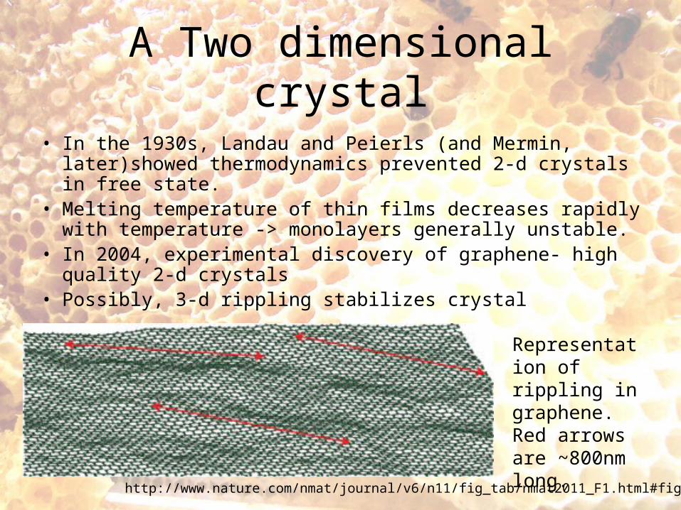
A Two dimensional crystal
• In the 1930s, Landau and Peierls (and Mermin, later)showed thermodynamics prevented 2-d crystals in free state.
• Melting temperature of thin films decreases rapidly with temperature -> monolayers generally unstable.
• In 2004, experimental discovery of graphene- high quality 2-d crystals
• Possibly, 3-d rippling stabilizes crystal
http://www.nature.com/nmat/journal/v6/n11/fig_tab/nmat2011_F1.html#figure-title
Representation of rippling in graphene. Red arrows are ~800nm long.

How to make graphene
• Strangely cheap and easy.• Either draw with a piece of graphite, or repeatedly peel with Scotch tape
• Place samples on specific thickness of Silicon wafer. The wrong thickness of silicon leaves graphene invisible.
• Graphene visible through feeble interference effect. Different thicknesses are different colors.

Samples of graphenea) Graphite films
visualized through atomic force microscopy.
b) Transmission electron microscopy image
c) Scanning electron microscope image of graphene.
A. K. Geim & K. S. Novoselov. The rise of graphene. Nature Materials Vol 6 183-191 (March 2007)

Electrons in graphene• Electrons in p-orbitals above and below plane
• p-orbitals become conjugated across the plane
• Electrons free to move across plane in delocalized orbitals
• Extremely high tensile strength
http://en.wikipedia.org/wiki/Aromaticity
-Graphene and graphite are great conductors along the planes.

Properties: charge carriers• Samples are excellent- graphene is ambipolar: charge carrier concentration continuously tunable from electrons to holes in high concentrations
A. K. Geim & K. S. Novoselov. The rise of graphene. Nature Materials Vol 6 183-191 (March 2007)
Relativistic charge carriers
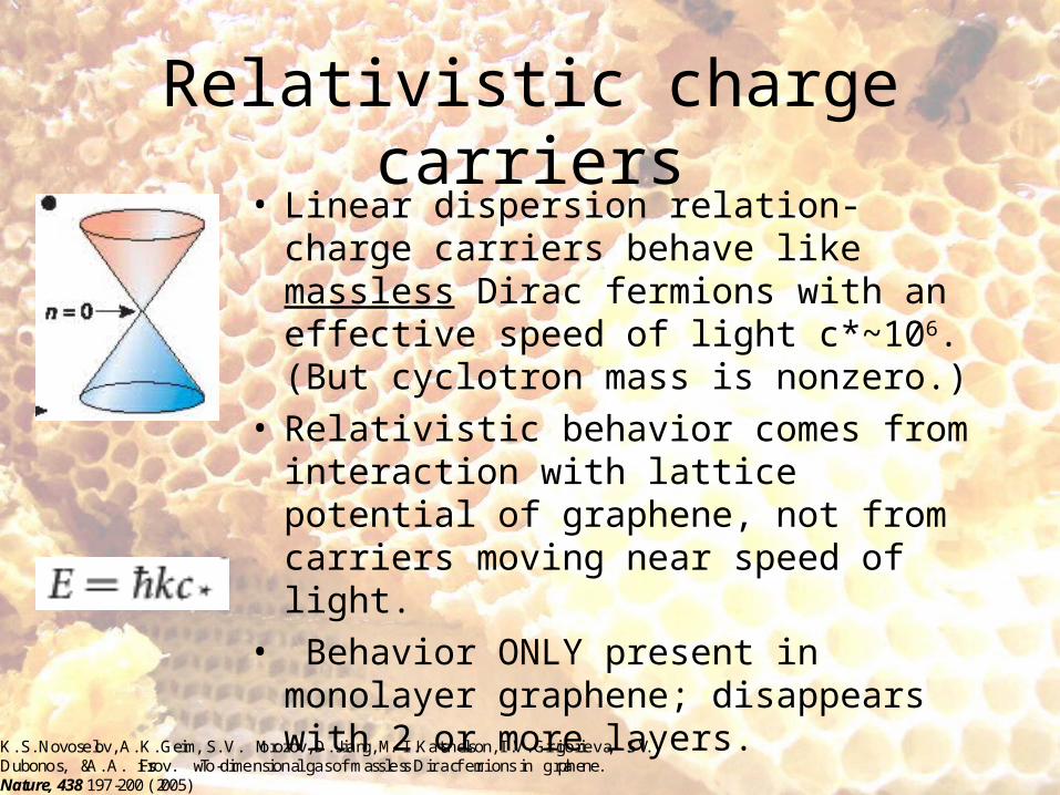
• Linear dispersion relation- charge carriers behave like massless Dirac fermions with an effective speed of light c*~106. (But cyclotron mass is nonzero.)
• Relativistic behavior comes from interaction with lattice potential of graphene, not from carriers moving near speed of light.
• Behavior ONLY present in monolayer graphene; disappears with 2 or more layers.K. S. Novoselov, A. K. Geim, S. V. Morozov, D. Jiang, M. I. Katsnelson, I. V. Grigorieva, S. V.
Dubonos, & A. A. Firsov. Two-dimensional gas of m assless Dirac fermions in graphene.Nature, 438 197-200 (2005)

GRAPHENE PN JUNCTIONS
•SELF ASSEMBLED MONOLAYERS CREATE A PN JUNCTIONS IN GRAPHENE FILMS
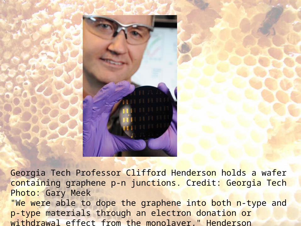
Georgia Tech Professor Clifford Henderson holds a wafer containing graphene p-n junctions. Credit: Georgia Tech Photo: Gary Meek"We were able to dope the graphene into both n-type and p-type materials through an electron donation or withdrawal effect from the monolayer," Henderson explained.

"That doesn't lead to the substitutional defects that are seen with many of the other doping processes. The graphene structure itself is still pristine as it comes to us in the transfer process."
Chemical Vapor Deposition (CVD) In this process, the substrate is placed inside a reactor to which a number of gases are supplied. The fundamental principle of the process is that a chemical reaction takes place between the source gases. The product of that reaction is a solid material with condenses on all surfaces inside the reactor. The two most important CVD technologies in MEMS are the Low Pressure CVD (LPCVD) and Plasma Enhanced CVD (PECVD). The LPCVD process produces layers with excellent uniformity of thickness and material characteristics. The main problems with the process are the high deposition temperature (higher than 600°C) and the relatively slow deposition rate..

The PECVD process can operate at lower temperatures (down to 300° C) thanks to the extra energy supplied to the gas molecules by the plasma in the reactor. However, the quality of the films tend to be inferior to processes running at higher temperatures.
Secondly, most PECVD deposition systems can only deposit the material on one side of the wafers on 1 to 4 wafers at a time. LPCVD systems deposit films on both sides of at least 25 wafers at a time.
Graphene and it's Applications: Electrodes with very high surface area and very low electrical resistance.
Transistors that operate at higher frequency.
Very high tensile strengthReplacement of nanotubes for cheapness in some applications: composite materials and batteries for improved conductivity
Conclusion• Graphene is a novel material with very unusual properties
• Easy to make in lab; may prove easy and economical to manufacture (unknown).
• Broad range of applications for future research.
• Variety of possible practical applications.

THANK YOU