Tunable optical absorption and interactions in graphene via oxygen plasma
30
1 Tunable optical absorption and interactions in graphene via oxygen plasma Iman Santoso 1,2,4,6 , Ram Sevak Singh 2 , Pranjal Kumar Gogoi 1,2,3 , Teguh Citra Asmara 1,2,3 , Dacheng Wei 2 , Wei Chen 2,4,5 , Andrew T.S. Wee 2,4 , Vitor M. Pereira 2,4,# , Andrivo Rusydi 1,2,3,* 1 NUSNNI-NanoCore, National University of Singapore, Singapore 117576 2 Department of Physics, National University of Singapore, Singapore 117542 3 Singapore Synchrotron Light Source, National University of Singapore, 5 Research Link, Singapore 117603, Singapore 4 Graphene Research Centre, Faculty of Science, National University of Singapore, Singapore 117546 5 Department of Chemistry, National University of Singapore, Singapore 117543 6 Jurusan Fisika,FMIPA, Universitas Gadjah Mada, BLS 21 Yogyakarta 55281, Indonesia * [email protected] # [email protected]
Transcript of Tunable optical absorption and interactions in graphene via oxygen plasma
1
Tunable optical absorption and interactions in graphene via oxygen plasma
Iman Santoso1,2,4,6, Ram Sevak Singh2, Pranjal Kumar Gogoi1,2,3, Teguh Citra Asmara1,2,3, Dacheng Wei2, Wei Chen2,4,5, Andrew T.S. Wee2,4, Vitor M. Pereira2,4,#, Andrivo Rusydi1,2,3,*
1NUSNNI-NanoCore, National University of Singapore, Singapore 117576 2Department of Physics, National University of Singapore, Singapore 117542 3Singapore Synchrotron Light Source, National University of Singapore, 5 Research Link,
Singapore 117603, Singapore 4Graphene Research Centre, Faculty of Science, National University of Singapore, Singapore
117546 5Department of Chemistry, National University of Singapore, Singapore 117543 6Jurusan Fisika,FMIPA, Universitas Gadjah Mada, BLS 21 Yogyakarta 55281, Indonesia
2
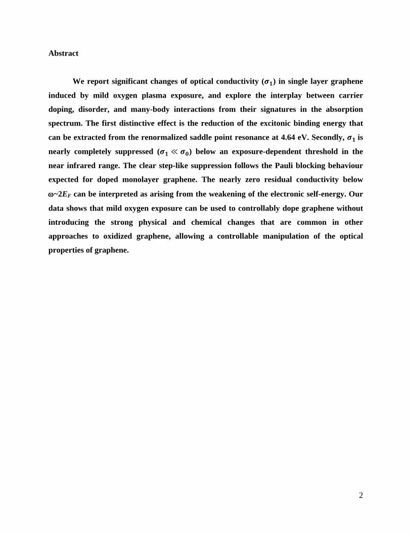
Abstract
We report significant changes of optical conductivity (𝝈𝟏) in single layer graphene
induced by mild oxygen plasma exposure, and explore the interplay between carrier
doping, disorder, and many-body interactions from their signatures in the absorption
spectrum. The first distinctive effect is the reduction of the excitonic binding energy that
can be extracted from the renormalized saddle point resonance at 4.64 eV. Secondly, 𝝈𝟏 is
nearly completely suppressed (𝝈𝟏 ≪ 𝝈𝟎) below an exposure-dependent threshold in the
near infrared range. The clear step-like suppression follows the Pauli blocking behaviour
expected for doped monolayer graphene. The nearly zero residual conductivity below
ω~2EF can be interpreted as arising from the weakening of the electronic self-energy. Our
data shows that mild oxygen exposure can be used to controllably dope graphene without
introducing the strong physical and chemical changes that are common in other
approaches to oxidized graphene, allowing a controllable manipulation of the optical
properties of graphene.
3
I. Introduction
In the absence of disorder, the optical conductivity of graphene –carbon atoms arranged
in a two dimensional hexagonal lattice – displays many remarkable optical properties, including
a broadband universal optical conductivity (𝜎0 = 𝜋𝑒2/2ℎ) in the infrared-to-visible range [1-4].
In the visible–ultraviolet range the interplay between electron-electron (e-e) and electron-hole (e-
h) interactions yields unique excitonic effects that renormalize and redshift the bare band
structure saddle point resonance by ~0.6 eV. This is clearly seen in the real part of the optical
conductivity (σ1) of graphene [3-9], and is one of the clear instances where explicit consideration
of many-body interactions is required for an accurate description of the electronic properties of
graphene. Recently, controlled disorder, such as defects, impurities, vacancies, and adatoms, has
been studied intensively and proposed as a means to tailor the transport and optical properties of
graphene [10-15]. For example, the functionalization of graphene using K, Rb [16] and NO2 [18]
have shown the large doping effects indicated by strong suppression of the absorption below 2EF
(EF is Fermi energy). Here we explore the optical response of graphene to controlled disorder
induced by oxygen plasma exposure.
Mild oxygen plasma exposure has been widely used to produce graphene oxide. This dry
method has numerous advantages, namely: the oxidation can take place rapidly, and it does not
strongly modify the transport properties of graphene. It is known that this method introduces
structural defects and electronic disorder due to the attachment of oxygen to carbon atoms, and to
the reduction in the overall sp2 order [18]. The fact that the oxygen arrives to the sample surface
by a process of diffusion, makes remote oxygen plasma treatment a clean way to control the
amount of disorder in graphene [18]. However, plasma exposure can have very different
outcomes in the optical and transport properties of graphene, depending on the intensity of
irradiation that directly translates into the degree of disorder and amorphization of the resulting
4
carbon lattice. Increased carrier densities, semiconducting transport behaviour, and
photoluminescence are frequently seen [18,19]. However, the electronic structure and correlation
effects in graphene with controlled disorder through the optical spectroscopy technique remain
unexplored. Hence, it is of great interest to study directly the optical absorption spectrum of
these systems, and analyse the interplay between carrier doping, disorder, and many-body
interactions from their signatures in the optical absorption spectrum.
Here, we study the evolution of optical conductivity, σ1(ω), of monolayer graphene in the
frequency range of 0.5–5.3 eV under mild (low power, ~6W) exposure to oxygen plasma. Single
layer graphene (SLG) was prepared on the surface of a copper foil via a low-pressure chemical
vapour deposition (CVD) process, and then transferred to a SiO2 (300nm)/Si substrate. Exposure
of SLG to the oxygen plasma is done in successive steps. After each 2-second (ts) exposure step
Raman scattering and spectroscopic ellipsometry (SE) measurements are performed on the
sample. The Raman traces are used to follow the level of disorder and amorphization in the
system following each exposure step. The spectroscopy ellipsometry measurements are used to
directly measure σ1(ω) in the spectral range 0.5–5.3 eV. As ts increases two important effects
emerge in the optical conductivity: the decrease of the resonant saddle-point peak intensity at 4.6
eV, concomitant with a significant reduction of the excitonic binding energy, and the dramatic
suppression of σ1 (close to zero) for photon energies below 1 eV.
II. Sample preparations and experimental methods
A low-pressure chemical vapour deposition (CVD) process was used to prepare SLG. A
copper foil was placed in the center of a horizontal 2 inch quartz tube furnace, and then was
annealed at 1000 °C in 10 sccm (150 mTorr ) H2 for 30 min. After that, 30 sccm CH4 was
5
introduced into the furnace as the carbon source for SLG growth, while the H2 was maintained at
10 sccm and the furnace temperature maintained at 1000 °C. The pressure was maintained at 350
mTorr in the growth. After 30 minutes the CH4 was turned off and the furnace was quickly
cooled down to room temperature in 10 sccm H2. To transfer SLG to a SiO2 (300 nm)/Si
substrate a PMMA film was spin-coated on the copper foil with SLG. After that, the copper foil
was etched in FeCl3 aqueous solution for 12 hours, and then a PMMA film with SLG can be
obtained on the solution surface. After cleaning the PMMA film in purified water for several
times, it was transferred to a SiO2 (300 nm)/Si substrate, and was heated at 180 °C for 2 min. To
remove the PMMA the substrate was placed in acetone vapor for 15 min and was annealed at
300 °C in 10 sccm H2 for 30 min. The SLG sample was then exposed to the mild oxygen plasma
for three consecutive durations of 2 s, 4 s, and 6 s using a radio-frequency (rf) plasma system.
The rf power was maintained at 6W and chamber pressure at 50 mTorr. The pristine SLG and
oxygen plasma exposed SLG were investigated using Raman and spectroscopy ellipsometry (SE)
measurements. Raman spectra were recorded using a 514 nm laser excitation wavelength
(Renishaw Raman measurement system). A low laser power of ~ 2 mW is employed to minimize
laser heating effects. All the measurements were performed at room temperature, in ambient, and
on the same sample. To check the stability of the sample we placed the sample in a dry box for
one day after SE measurements. After that, we repeated the SE measurements and the SE data
showed no significant change, indicating that the sample is stable enough for measurements in an
ambient environment.
Spectroscopic ellipsometry (SE) [34] measurements are performed on the graphene
sample and substrate (SiO2 (300 nm)/Si) using a SENTECH SE850 ellipsometer. This
ellipsometer is equipped with three different light sources, i.e. Deep UV ((deuterium), UV/VIS
6
source (Xe-lamp) and the NIR source (Halogen lamp of the FT-IR spectrometer), allowing us to
measure from 0.5 eV to 6.3 eV. For our measurements we used additional micro-focus probes
(~100 micron spot diameter) which work well in the range from 0.5 – 5.3 eV. SE allows the
accurate measurement of ellipsometric parameters Ψ and ∆ defined from the relation
tan(Ψ)exp(iΔ) = 𝑟𝑝𝑟𝑠
, where 𝑟𝑝 and 𝑟𝑠 are the complex reflection amplitudes for the p and s light
polarizations. Thus, Ψ represents the ratio between the amplitude of p and s polarized reflected
light while ∆ represents the phase difference between p and s polarized reflected light.
III. Results and discussion
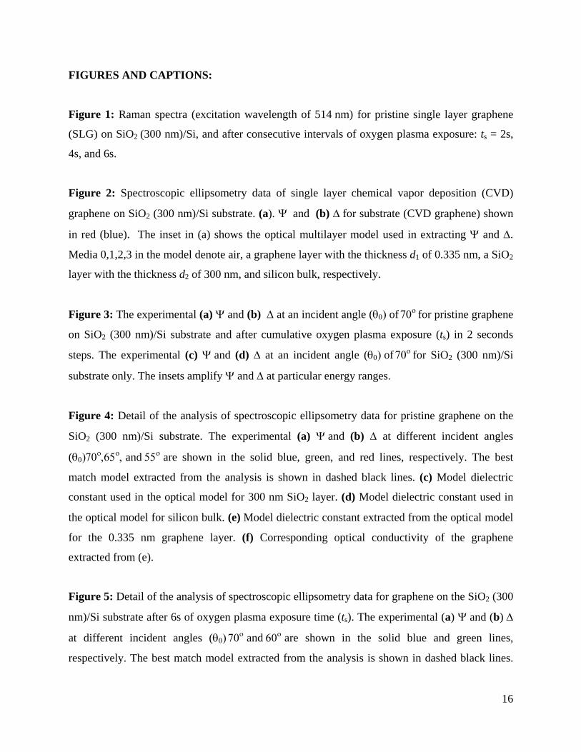
In Figure 1 we show the Raman spectra for graphene on SiO2 before (pristine) and after
exposure to oxygen plasma for 2s, 4s, and 6s. The high quality of our pristine graphene is
confirmed by the very sharp Raman G peak at 1593 cm-1 with a full width at half maximum
(FWHM) of 20 cm-1, a 2D peak at 2694 cm-1 with FWHM of 36 cm-1, and no evidence of defect
scattering (absent D peak). Furthermore, the 2D to G peak intensity ratio (I2D/IG) is around two,
and the 2D peak possesses a symmetric single Lorentzian shape. This, together with the
behaviour of the σ1 (see below) indicates that our system consists of monolayer graphene [20].
Upon exposure to oxygen plasma, the appearance of the D and D’ peaks at ~1318 cm-1 and 1615
cm-1, respectively, indicates pronounced inter- and intra-valley scattering [19-22]. After the first
exposure, we observe a decrease in the ratio between the D and G peak intensities (ID/IG), which
changes from 1.65 to 0.95 with growing ts. The fact that the D and D’ peaks are intense and
broad for ts > 2s suggests relatively strong disorder. Furthermore, based on the three-stage model
of structural disorder in graphitic materials [23], our oxidized samples are likely in stage two. In
this stage the decrease of (ID/IG) is due to the decrease in the number of sp2 ordered rings, and is
7
related to the in-plane crystalline grain size (La) through the empirical formula: 𝐼𝐷 𝐼𝐺 = 𝐶′(𝜆)𝐿𝑎2⁄ ,
where 𝐶′(𝜆) denotes a constant at the particular excitation wavelength (λ) used in Raman
measurements. Here we use C’(514 nm) = 0.55 nm-2 [18,23].
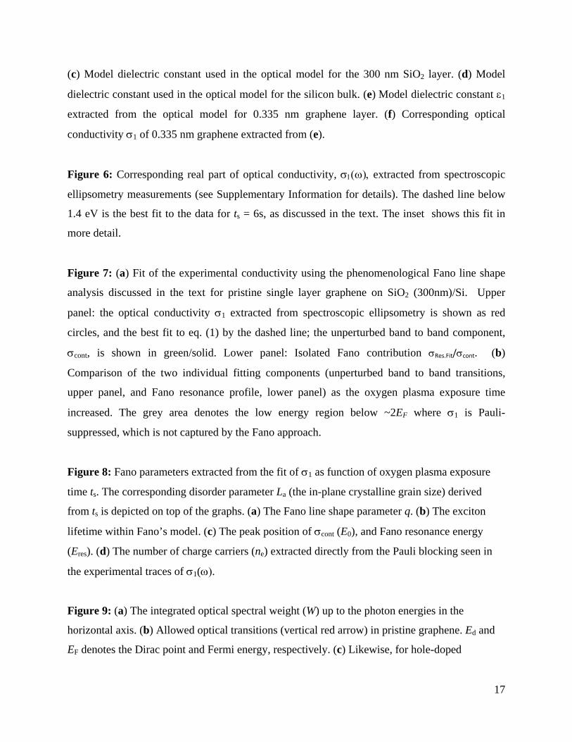
Spectroscopy Ellipsometry data for Ψ and ∆ are taken at multiple incident angles and at
several spots on the sample. The data at different spots are identical in almost all cases which
show sample homogeneity. The multiple incident angle data is required for global fitting of the
data. SE measurement is generally preferable because it gives both the real and imaginary parts
of the dielectric function directly, whereas other measurement techniques (such as direct
reflectivity) require a Kramers-Kronig transformation. Moreover, in case of very thin films the
change in phase of the incident light waves upon reflection is much more pronounced than the
change in amplitude of the light of different polarizations. These two facts make SE an ideal
method for analyzing systems like the very thin monolayer of graphene on a substrate. In Figure
2 we show the measured Ψ and ∆ values of samples with and without graphene on substrate at
70o incident angle. The spectra show a pronounced contrast due to the presence of graphene
which is only ~3 Angstrom thick.
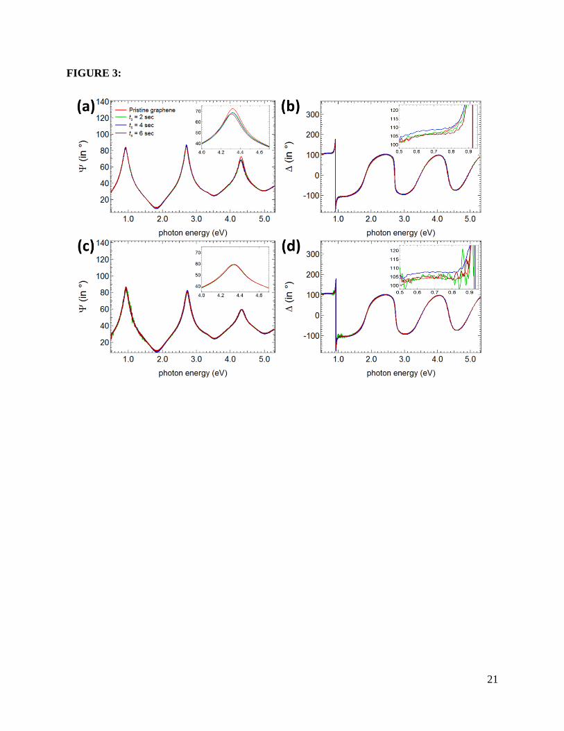
We show the experimental Ψ and ∆ of pristine graphene on the SiO2 (300 nm)/Si
substrate and after cumulative oxygen plasma exposure (ts) in 2 seconds steps in Figs. 3 (a) and
(b). Due to oxygen plasma exposure, Ψ and ∆ are slightly changed, especially in the energy
range indicated in the inset of Figs. 3 (a) and (b). These facts show that the optical constants (e.g.
dielectric constant and hence optical conductivity) changed and care should be taken when the
fitting procedure is applied in these particular energy ranges. In contrast, within the error bars of
the measurements, there is no significant change of the measured Ψ and ∆ of the SiO2 (300
8
nm)/Si substrate after cumulative oxygen plasma exposure (see Figs. 3(c) and (d) as well as the
insets).
To extract the optical constants, the system is modeled with Fresnel coefficients for an
optical multilayered film system (see inset of Fig. 2 (a)). The model is composed of a silicon
bulk (label 3), a 300 nm SiO2 layer (label 2), a 0.335 nm graphene layer (label 1), and the air
(label 0). The Fresnel coefficients of reflected light for each interface of two adjacent layers are
given by [34-36]:
𝑟01,𝑝 = √𝜀1 cos𝜃0−�𝜀0 cos𝜃1√𝜀1 cos𝜃0+�𝜀0 cos𝜃1
; 𝑟01,𝑠 = �𝜀0 cos𝜃0−√𝜀1 cos𝜃1�𝜀0 cos𝜃0+√𝜀1 cos𝜃1
, (1)
where we have implicitly applied the Fresnel equation for the interface between medium 0 (air)
and medium 1 (graphene layer) in deriving eq.(1). The p and s denote the p and s polarization of
light, respectively. The ε0 and ε1 represent the dielectric constant of medium 0 and medium 1. θ0
and θ1 represent the incident angle and refracted angle at the interface between medium 0 and
medium 1. These angles are related to each other by Snell’s law. The Fresnel coefficients of
reflected light for other interfaces (e.g. r12 and r23) can be obtained by substituting the index 0
and 1 in eq.(1) with the respective index under consideration. The total amplitude of the
reflection of the system given in the inset of Fig. 2 (a) is [34-36]:
𝑟0123,𝑝(𝑠) = 𝑟01,𝑝(𝑠)+𝑟12,𝑝(𝑠)exp(−𝑖2𝛽1)+[𝑟01,𝑝(𝑠)𝑟12,𝑝(𝑠)+exp(−𝑖2𝛽1)]𝑟23,𝑝(𝑠)exp(−𝑖2𝛽2)
1+𝑟01,𝑝(𝑠)𝑟12,𝑝(𝑠)exp(−𝑖2𝛽1)+[𝑟12,𝑝(𝑠)+𝑟01,𝑝(𝑠)exp(−𝑖2𝛽1)]𝑟23,𝑝(𝑠)exp(−𝑖2𝛽2) , (2)
Where p(s) denotes p(s) polarized light; 𝛽1 and 𝛽2 represent the phase difference when light
penetrates through the interface between medium 0 and 1, and between medium 2 and 3,
respectively. 𝛽1 and 𝛽2 are given by 𝛽1 = 2𝜋𝑑1𝜆
[𝜀1 − 𝜀0sin2𝜃0]1 2⁄ and 𝛽2 = 2𝜋𝑑2𝜆
[𝜀2 −
9
𝜀0sin2𝜃0]1 2⁄ . d1 and d2 are the thickness of the layer 1 and layer 2 while λ denotes the
wavelength of the light source used in this experiment.
The dielectric constants of the SiO2 and silicon bulk are extracted from a fit of the
experimental Ψ and ∆ of the substrate with an optical model comprised of a 300 nm SiO2 layer
and silicon bulk (see the inset of Fig. 2 (a) with red arrow). In extracting these dielectric
constants, we use many oscillators which can be described by Drude-Lorentz model [35,36]:
ε(ω) = ε∞ + ∑ωp,k2
ω0,k2 −ω2−iγkωk , (3)
where 𝜀∞ denotes the high-frequency dielectric constant, which represents the contribution from
all oscillators at very high frequencies compared to the frequency ranges under examination. The
parameters 𝜔𝑝,𝑘 , 𝜔𝑜,𝑘 and 𝛾𝑘 are the plasma frequency, the transverse frequency
(eigenfrequency) and the linewidth (scattering rate), respectively, of the k-th Lorentz oscillator.
For the SiO2 layer we have used one additional oscillator at high energy (~9 eV) in order to
capture the first absorption peak in SiO2 [37] and, hence, give the best match between the model
and the experimental Ψ and ∆. Alternatively, one can use the Cauchy layer for describing the
SiO2 layer [38]. The obtained dielectric constants of the SiO2 and silicon bulk used for extracting
the dielectric constant of graphene based on the optical model are shown in the inset of Fig. 2 (a)
(with a blue arrow). We assume that the graphene film is flat and isotropic [38-40]. Having
extracted the complex 𝜀(𝜔) = 𝜀1(𝜔) + 𝑖𝜀2(𝜔), σ1(ω) follows immediately from
𝜎1 = 𝜔𝜀24𝜋
. (4)
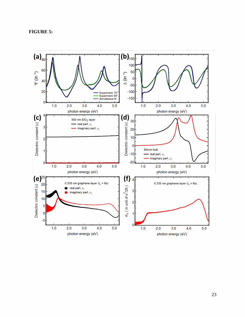
Figures 4 and 5 plot the detailed analysis of SE data for pristine graphene on SiO2 (300 nm)/Si
substrate and after 6 seconds of oxygen plasma exposure time (ts), respectively. The shaded area
10
in ε1 and σ1 (Figs. 5 (a) and (b)) indicates the range in which the model can still match the
experimental Ψ and ∆ (within the error bars).
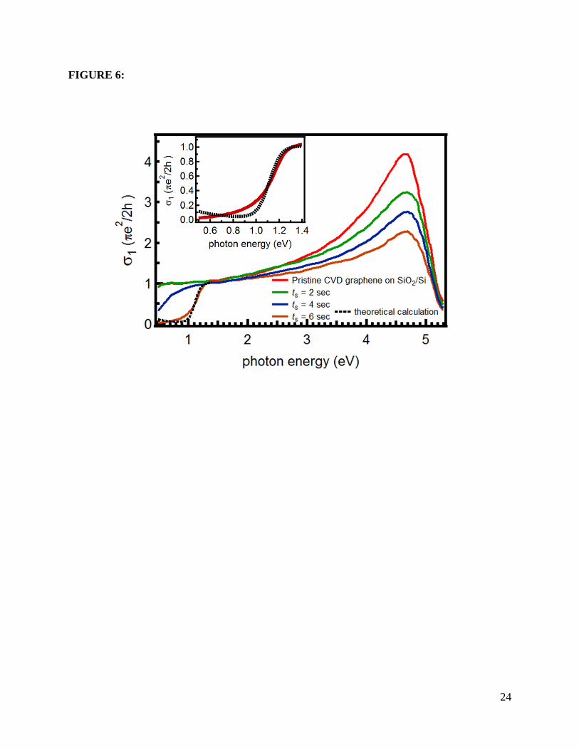
In the next discussion, we concentrate on the evolution of σ1 as function of ts as shown in
Figure 6. In addition to the Raman characterization, the monolayer character of our sample is
further corroborated by the constancy and magnitude of σ1 at low frequencies, which rather
accurately coincides with the universal value 𝜎0 = 𝜋𝑒2/2ℎ expected for a graphene monolayer
[31]. The two main effects of oxygen exposure are: (1) a significant reduction (more than 50 %)
of the van Hove peak intensity at 4.64 eV in the ultraviolet (UV) range, accompanied by a large
blue-shift of the peak position; (2) σ1 is gradually suppressed to zero in a step-like fashion as ts
increases in the near infrared (NIR) range. We now discuss these two observations in more
detail.
A prominent asymmetric peak in σ1 at 4.64 eV can be attributed to excitonic
renormalization of the independent particle optical transitions at the M point (i.e. van Hove
singularity (VHS)) in the Brillouin zone of the graphene band structure. If one considers only
direct band to band transitions using a local density approximation (LDA) the optical transition
peak should occur at ω~4.1 eV. By accounting for e-e interactions within a GW approach the
optical transition peak is predicted to lie at 5.2 eV, and further incorporating e-h interactions the
peak is red-shifted by ~600 meV from 5.2 eV to 4.6 eV [4-8]. This is precisely the position of the
peak measured here for the pristine sample, as seen in Fig. 6.
In order to quantify the interplay between e-e and e-h interactions that manifests itself in
the renormalization of the bare VHS peak in our controlled disorder graphene we employ the
Fano phenomenological approach since, as seen previously, the asymmetric peak measured here
at 4.64 eV resembles a Fano profile. Following Fano’s model, the asymmetric line shape in the
11
optical spectra can be thought of as arising from the coupling of the continuum electronic states
near the saddle point singularity (M point) to discrete sharp excitonic states [24,25]. The
resultant σ1 in the presence of this Fano resonance can be described by [7]:
𝜎1𝜎1,𝑐𝑜𝑛𝑡
= (𝑞+𝜀)2
1+𝜀2, (5)
where 𝜎1,cont(𝜔) represents the continuum contribution to σ1 arising from band-to-band
transitions at the M point (possibly renormalized by e-e interactions [5]), 𝜀 = 2(𝜔−𝐸res)𝛤
, Γ is a
phenomenological width related to the lifetime of the exciton, and Eres denotes the resonance
energy. The parameter q determines the lineshape, while q2 gives the ratio of the strength of the
excitonic transition to the unperturbed band-to-band transition. For simplicity, to capture
quantitatively the spectral features in the vicinity of the resonance, we model σcont with a
constant background plus the logarithmic singularity in the joint density of states (JDOS) at the
M point: 𝜎1, cont(𝜔) = −𝐴 𝑙𝑜𝑔 �1 − 𝜔𝐸0� � ⊗ 𝑅𝐺(𝜔) + 𝐶, where A is a scaling factor, E0 the
unperturbed band to band transition energy, and 𝑅𝐺(𝜔) is a Gaussian of width EBr = 0.25 eV that
is convoluted with the bare divergence to account for the finite broadening [7]. The constant
background (C) is intended to capture the universal optical conductivity (𝜎0) of graphene at low
frequencies.
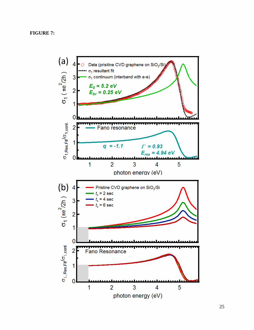
Figure 7(a) shows the best fit of σ1 for pristine single layer graphene using the
phenomenological Fano analysis with the parameters q = -1.1, Γ = 0.93 eV, 𝐸𝑟𝑒𝑠 = 4.94 eV, and
𝐸0 = 5.2 eV. Despite the simplicity of the assumption used for σcont, the result of fitting eq. (5)
to the data in the energy range between 0.5 to 5.0 eV captures the overall behaviour of the
conductivity very well, including the universal σ1 at lower energy and the main features of the
renormalized van Hove peak. Figure 7(b) shows the separate contributions of 𝜎1,cont (upper
12
panel) and the Fano resonance (lower panel) to the resulting σ1, as a function of the oxygen
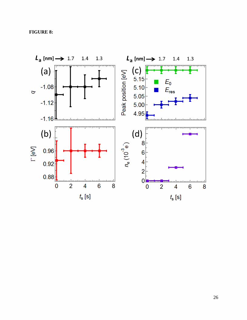
exposure time. Figures 8(a), (b), and (c) show the dependence of Fano parameters q, Γ, ERes, and
E0, respectively, on the amount of disorder. The symmetric peak at 5.25 eV in 𝜎cont coming from
the unperturbed band-to-band transitions (see Fig.7(b)) decreases significantly to 50% in
intensity without any shift in energy, as quantified in Figure 8(c). As for the contribution of the
Fano resonance, it shows no significant change in shape as inferred from their q and Γ values,
which barely change within the error bars (Figures 2(a) and (b)). However, a gradual blue shift as
high as 100 meV is observed in the energy of the Fano resonance, as seen in Figure 3(c), where
we show the position of the Fano resonance and the peak in σcont that best fit each experimental
curve for σ1(ω). This variation of ERes suggests a considerable reduction of the excitonic binding
energy (by 100 meV for ts=6 s) upon oxygen exposure, whereas the persistence of the line shape
indicates that, even though weakened upon oxygen exposure, the nature of the interaction itself
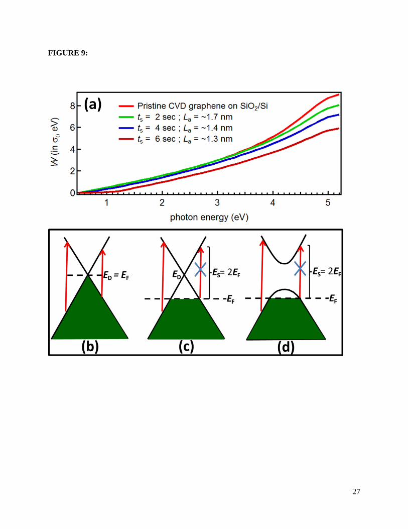
has not changed. We consider now the dramatic suppression observed in σ1 at frequencies below
1eV. Oxygen plasma hole-dopes graphene and might, or might-not, introduce strong
renormalization of the band structure, depending on the amount of disorder, and how the
oxidation affects the graphene lattice. Given that the overall profile of σ1(ω) retains all the
features of pristine graphene, we interpret the suppression of σ1 at low frequencies as due to
simple Pauli blocking, which excludes inter-band transitions for frequencies below 2EF (see
Figures 9(b) and 4(c)) [2]. For definiteness, and given that our lower experimental frequency
limit is 0.5 eV, we explicitly compare the curve at the highest exposure time (that shows a clear
suppression of absorption) with the expected frequency-dependent conductivity of doped SLG.
Within a Kubo approach it reads [32]
𝜎1(𝜔)𝜎0
= 8𝜋� 2𝛾𝑘𝐵𝑇𝜔2+4𝛾2
� 𝑙𝑜𝑔 �2𝑐𝑜𝑠ℎ � 𝐸𝐹2𝑘𝐵𝑇
�� + 𝑓 �−𝜔2� − 𝑓 �𝜔
2�, (6)
13
where 2γ represents the half-width of the Drude peak and f(E) is the usual Fermi-Dirac
distribution function. The dashed line below ω=1.4 eV in Fig. 6 shows the best fit of this
expression to the experimental data at 300 K. From it we obtain EF=0.558±0.003 eV and
γ =0.021±0.004 eV (≈170 cm-1). Despite the absence of data below 0.5 eV for direct
confirmation, this value is in reasonable agreement with the Drude width expected for graphene
grown by CVD on Cu under high electron doping (>100 cm-1) [33]. Assuming that the graphene
dispersion remains linear after oxygen exposure, we can estimate the number of charge carriers
(ne) per unit cell as 𝑛𝑒 = 𝐴 |𝐸𝐹|2
𝜋(ℏ𝑣𝐹)2 , where A is the area of the graphene unit cell, and EF can be
extracted from the fit to the equation above. Figure 8(d) shows the dependence of ne on oxygen
exposure. Moreover, in graphene the integrated spectral weight (W) in the NIR is conserved, and
density independent: ∫ 𝜎(𝜔)𝑑𝜔𝜔𝑀0 ≃ 𝜎0𝜔𝑀, when the integration limit 𝜔𝑀 ≫ 2𝐸𝐹. This
integrated spectral weight is shown in Figure 9(a), and allows us to check the consistency of the
extracted EF directly from the relative changes in optical spectral weight with different exposure
times. The doping scenario is also consistent with the slight exposure-induced shift of the Raman
G peak in our Raman data in Figure 1 [18,26]. The fact that the peak position changes only ~40
meV (Fig. 8(c)) from ts= 2s to 6s while ne changes by an order of magnitude, (Fig. 8(d)) suggests
the complex interplay between disorder and doping in the optical spectra.
What is striking in our optical data in this region is the very large suppression of σ1
below 2EF (Figure 6, ts = 6s), when the optical response of doped graphene in the Pauli-blocked
region is usually characterized by a residual conductivity ~0.2-0.4σ0 [27]. Such a residual
conductivity can be justified theoretically on the basis of a finite electronic self-energy whose
imaginary part is linear in ω [28]. The self-energy contributions can arise from the marginal
Fermi liquid character of the electron-electron interactions in graphene, as well as optical
14
phonons or disorder [29,30]. Our Raman data shows that the optical phonons are clearly affected
by the oxygen exposure, and the Fano analysis of the optical data around the VHS reveals the
clear suppression of the excitonic binding energy, thus hinting at reduced interactions with
increased exposure times. Together these effects can lead to the suppression of the marginal
Fermi liquid self-energy, thus explaining the nearly zero optical absorption below 2EF. Since our
samples are disordered, it would also imply that the dominant mechanism for the residual optical
conductivity in the Pauli-blocked region might indeed lie in interaction effects, rather than
disorder. Finally, we underline that our plasma exposure is much milder than the intensities
employed in recent reports, which reveal pristine graphene transitioning from ambipolar metallic
to insulating behaviour upon treatment with oxygen plasma [18,19], whereas our samples retain
the overall graphene signature in the frequency dependent optical conductivity.
IV. Conclusion
In summary, we reported ellipsometry and Raman spectroscopic measurements on
monolayer graphene exposed to mild oxygen plasma. We see that it affects the magnitude of
electronic interactions from the reduction of the excitonic binding energy in the UV range, and
from the nearly zero residual optical conductivity in the Pauli-blocked NIR range, which,
according to existing interpretations for that residual optical absorption, is consistent with the
weakening of the electronic self-energy. Our data suggests, in addition, that low levels of oxygen
plasma exposure can be used as a controllable means to tune the optical absorption in graphene,
without disrupting the overall graphene optical response, contrary to what happens in other
oxygenation or doping strategies. Finally, it remains an open question with regard to IR spectral
region below 0.5 eV where important details might lie for the full picture of the effects of mild

15
oxygenation, including details of the Drude region and spectral weight redistribution. The results
reported here certainly warrant further investigation of this spectral region in the future.
Acknowledgment
We are grateful to Antonio H. Castro Neto for very useful discussions. This work is
supported by Singapore National Research Foundation under its Competitive Research Funding
scheme of “Control of Exotic Quantum Phenomena at Strategic Interfaces and Surfaces for
Novel Functionality by in-situ Synchrotron Radiation” and “Tailoring Oxide Electronics by
Atomic Control”, and MOE-AcRF-Tier-2, NUS-YIA and FRC. VMP is supported by the NRF-
CRP grant R-144-000-295-281.
16
FIGURES AND CAPTIONS:
Figure 1: Raman spectra (excitation wavelength of 514 nm) for pristine single layer graphene
(SLG) on SiO2 (300 nm)/Si, and after consecutive intervals of oxygen plasma exposure: ts = 2s,
4s, and 6s.
Figure 2: Spectroscopic ellipsometry data of single layer chemical vapor deposition (CVD)
graphene on SiO2 (300 nm)/Si substrate. (a). Ψ and (b) ∆ for substrate (CVD graphene) shown
in red (blue). The inset in (a) shows the optical multilayer model used in extracting Ψ and ∆.
Media 0,1,2,3 in the model denote air, a graphene layer with the thickness d1 of 0.335 nm, a SiO2
layer with the thickness d2 of 300 nm, and silicon bulk, respectively.
Figure 3: The experimental (a) Ψ and (b) ∆ at an incident angle (θ0) of 70ο for pristine graphene
on SiO2 (300 nm)/Si substrate and after cumulative oxygen plasma exposure (ts) in 2 seconds
steps. The experimental (c) Ψ and (d) ∆ at an incident angle (θ0) of 70ο for SiO2 (300 nm)/Si
substrate only. The insets amplify Ψ and ∆ at particular energy ranges.
Figure 4: Detail of the analysis of spectroscopic ellipsometry data for pristine graphene on the
SiO2 (300 nm)/Si substrate. The experimental (a) Ψ and (b) ∆ at different incident angles
(θ0)70ο,65ο, and 55ο are shown in the solid blue, green, and red lines, respectively. The best
match model extracted from the analysis is shown in dashed black lines. (c) Model dielectric
constant used in the optical model for 300 nm SiO2 layer. (d) Model dielectric constant used in
the optical model for silicon bulk. (e) Model dielectric constant extracted from the optical model
for the 0.335 nm graphene layer. (f) Corresponding optical conductivity of the graphene
extracted from (e).
Figure 5: Detail of the analysis of spectroscopic ellipsometry data for graphene on the SiO2 (300
nm)/Si substrate after 6s of oxygen plasma exposure time (ts). The experimental (a) Ψ and (b) ∆
at different incident angles (θ0) 70ο and 60ο are shown in the solid blue and green lines,
respectively. The best match model extracted from the analysis is shown in dashed black lines.
17
(c) Model dielectric constant used in the optical model for the 300 nm SiO2 layer. (d) Model
dielectric constant used in the optical model for the silicon bulk. (e) Model dielectric constant ε1
extracted from the optical model for 0.335 nm graphene layer. (f) Corresponding optical
conductivity σ1 of 0.335 nm graphene extracted from (e).
Figure 6: Corresponding real part of optical conductivity, σ1(ω), extracted from spectroscopic
ellipsometry measurements (see Supplementary Information for details). The dashed line below
1.4 eV is the best fit to the data for ts = 6s, as discussed in the text. The inset shows this fit in
more detail.
Figure 7: (a) Fit of the experimental conductivity using the phenomenological Fano line shape
analysis discussed in the text for pristine single layer graphene on SiO2 (300nm)/Si. Upper
panel: the optical conductivity σ1 extracted from spectroscopic ellipsometry is shown as red
circles, and the best fit to eq. (1) by the dashed line; the unperturbed band to band component,
σcont, is shown in green/solid. Lower panel: Isolated Fano contribution σRes.Fit/σcont. (b)
Comparison of the two individual fitting components (unperturbed band to band transitions,
upper panel, and Fano resonance profile, lower panel) as the oxygen plasma exposure time
increased. The grey area denotes the low energy region below ~2EF where σ1 is Pauli-
suppressed, which is not captured by the Fano approach.
Figure 8: Fano parameters extracted from the fit of σ1 as function of oxygen plasma exposure
time ts. The corresponding disorder parameter La (the in-plane crystalline grain size) derived
from ts is depicted on top of the graphs. (a) The Fano line shape parameter q. (b) The exciton
lifetime within Fano’s model. (c) The peak position of σcont (E0), and Fano resonance energy
(Eres). (d) The number of charge carriers (ne) extracted directly from the Pauli blocking seen in
the experimental traces of σ1(ω).
Figure 9: (a) The integrated optical spectral weight (W) up to the photon energies in the
horizontal axis. (b) Allowed optical transitions (vertical red arrow) in pristine graphene. Ed and
EF denotes the Dirac point and Fermi energy, respectively. (c) Likewise, for hole-doped

18
graphene. Optical transitions below Es are disallowed due to Pauli’s exclusion principle. (d) In
hole-doped and gapped graphene.
19
FIGURE 1:
20
FIGURE 2:
21
FIGURE 3:
22
FIGURE 4:
23
FIGURE 5:
24
FIGURE 6:
25
FIGURE 7:
26
FIGURE 8:
27
FIGURE 9:
28
REFERENCES :
1. A.H. Castro Neto, F. Guinea, N.M.R. Peres, K.S. Novoselov, and A.K. Geim, Rev. Mod. Phys. 81, 109 (2009).
2. N.M. Peres, Rev. Mod. Phys. 82, 2673 (2010).
3. I. Santoso, P. K. Gogoi, H.B. Su, H. Huang, Y. Lu, D. Qi, W. Chen, M. A. Majidi, Y.P Feng, A.T.S. Wee, K.P. Loh, T. Venkatesan, R.P. Saichu, A. Goos, A. Kotlov, M. Ruebhausen, and A. Rusydi, Phys. Rev. B 84, 081403R (2011).
4. P.K. Gogoi, I. Santoso, S. Saha, S. Wang, A.H. Castro Neto, K.P. Loh, T. Venkatesan, A. Rusydi, Europhys. Lett. 99, 67009 (2012).
5. L. Yang, J. Deslippe, C.H. Park, M.L. Cohen, and S.G. Louie, Phys. Rev. Lett. 103,186802 (2009).
6. V.G. Kravets et al., Phys. Rev. B 81, 155413 (2010).
7. K.F. Mak, J. Shan, and T.F. Heinz, Phys. Rev. Lett. 106, 046401 (2011).
8. D.H. Chae et al., Nano Lett. 11, 1379 (2011).
9. V.N. Kotov, B. Uchoa, V.M. Pereira, F. Guinea, and A.H. Castro Neto, Rev. Mod. Phys. 84, 1067 (2012).
10. J. H. Chen, W.G. Cullen, C. Jang, M.S. Fuhrer, and E.D. Williams, Phys. Rev. Lett. 102, 236805 (2009).
11. J.H. Chen et al., Nat. Phys. 4, 377 (2008).
12. D.C. Elias et al., Science 323, 610 (2009).
13. T.O. Wehling, S. Yuan, A.I. Lichtenstein, A.K. Geim, and M. I. Katsnelson, Phys. Rev. Lett. 105, 056802 (2010).
14. S. Yuan, R. Roldan, H. de Raedt, and M.I. Katsnelson, Phys. Rev. B 84, 195418 (2011).
15. V.M. Pereira et al., Phys. Rev. Lett. 96, 036801 (2006). 16. N. Jung, B. Kim, A.C. Crowther, N. Kim, C. Nuckolls, and L. Brus, ACS Nano 5, 5708
(2011).
17. A.C. Crowther, A. Ghassaei, N. Jung, L.E. Brus, ACS Nano 6, 1865 (2012).
18. D.C. Kim, D.Y. Jeon, H.J. Chung, Y.S. Woo, J.K. Shin and S. Seo, Nanotechnology 20, 375703 (2009).
29
19. A. Nourbakhsh et al., Nanotechnology 21, 435203 (2010).
20. A. C. Ferrari et al., Phys. Rev. Lett. 97, 187401 (2007).
21. L. G. Cancado, M. A. Pimenta, B. R. A. Neves, M. S. S. Dantas, and A. Jorio, Phys. Rev. Lett. 93, 247401 (2004).
22. M. A. Pimenta et al., Phys. Chem. Chem. Phys. 9, 1276 (2007).
23. A. C. Ferrari and J. Robertson, Phys. Rev. B 61, 14095 (2000).
24. U. Fano, Phys. Rev. 124, 6, 1866 (1961).
25. J. C. Phillips, Excitons. In The Optical Properties of Solids; Tauc, J., Ed.; Academic Press: New York, (1966).
26. J. Yan, Y. Zhang, P. Kim, and A. Pinczuk, Phys. Rev Lett. 98, 166802 (2007). 27. Z.Q. Li, et al.et al., Nature Physics 4, 532 (2008). 28. A.G. Grushin, B. Valenzuela, and M.A.H. Vozmediano, Phys. Rev. B 80, 155417 (2009). 29. T. Stauber, N.M.R. Peres, and A. H. Castro Neto, Phys. Rev. B 78, 085418 (2008). 30. T. Ando, Y. Zheng, and H. Suzuura, J. Phys. Soc. Jpn. 71, 1318 (2002). 31. R.R. Nair et al. Science 320, 1308 (2008). 32. V.P. Gusynin, S.G. Sharapov, and J.P. Carbotte, New J. Phys. 11, 095013 (2009). 33. J. Horng et al. Phys. Rev. B 83, 165113 (2011). 34. R. M. A. Azzam, N. M. Bashara, Ellipsometry and Polarized Light, North-Holland,
Amsterdam (1977). 35. H. Fujiwara, Spectroscopic Ellipsometry Principles and Applications, John-Wiley and
Sons 2007. 36. M. Born and E. Wolf, Principles of optics : Electromagnetic theory of propagation,
interference and diffraction of light, 7th edition, Cambridge university press 1999 . 37. G. L. Tan, M. F. Lemon, D. J. Jones, and R. H. French, Optical properties and London
dispersion interaction of amorphous and crystalline SiO2 determied by vacuum ultraviolet spectroscopy and spectroscopic ellipsometry. Phys. Rev. B 72, 205117 (2005).
30
38. F. J. Nelson, V. K. Kaminen, T. Zhang, E. S. Comfort, J. U. Lee, A. C. Diebold, Optical properties of large-area polycrystalline chemical vapor deposited graphene by spectroscopic ellipsometry. Appl. Phys. Lett., 97, 253110 (2010).
39. J. W. Weber, V. E. Calado, M. C. M. van de Sanden, Optical constants of graphene
measured by spectroscopic ellipsometry. Appl. Phys. Lett., 97, 091904 (2010). 40. A. Boosalis, T. Hofmann, V. Darakchieva, R. Yakimova, and M. Schubert, Visible to
vacuum ultraviolet dielectric functions of epitaxial graphene on 3C and 4H SiC polytypes determined by spectroscopic ellipsometry. Appl. Phys. Lett., 101, 011914 (2012).