Tunable Electroluminescence in Planar Graphene/SiO 2 Memristors
6
© 2013 WILEY-VCH Verlag GmbH & Co. KGaA, Weinheim 1 www.advmat.de www.MaterialsViews.com wileyonlinelibrary.com COMMUNICATION Tunable Electroluminescence in Planar Graphene/SiO 2 Memristors Congli He, Jiafang Li, Xing Wu, Peng Chen, Jing Zhao, Kuibo Yin, Meng Cheng, Wei Yang, Guibai Xie, Duoming Wang, Donghua Liu, Rong Yang, Dongxia Shi, Zhiyuan Li, Litao Sun, and Guangyu Zhang* Since the first prototype was announced in 2008, [1] mem- ristors [2] have attracted broad interests over the past several years due to their potentials for non-volatile memory, [3,4] arti- ficial neural networks, [5,6] chaotic circuits, [7,8] logic operation, [9] signal processing, [10] and so on. The resistance of a memristor can change under the action of electric field or current, and this change is non-volatile and reversible. A broad category of materials and structures have been included in memristors, and a typical memristor is constructed from either capacitor- like or planar metal-oxide-metal (MIM) structures. [11,12] While most of current research on MIM memristors focus on their electronic behaviors, their optical properties, especially the electroluminescence (EL) related to their resistance states, i.e. high resistance state (HRS) and low resistance state (LRS), were rarely investigated. [13–15] Here we report the first realization of the electroluminescence and the resistive switching simultane- ously in the same planar nanogapped memristor device. These devices have planar MIM structures using nanogapped gra- phene as electrodes and SiO 2 as dielectric layer. The light emis- sion ranging at 400–1100 nm that can be tuned by the device’s resistance states was found, and prototype of light-emitting sources for displays and pulsed signaling were demonstrated. An electron-hole recombination EL mechanism for Si nanocrys- tals (NCs) in these devices was proposed and evidenced by our spectroscopic and structural characterizations. The combina- tion of memristor and EL may bring new functionalities for this type of devices, e.g. potential use of these optical signals to detect the devices’ resistance states. Our results may be very important for future nanoelectronic and optoelectronic applica- tions, such as a very promising light source, light-pulse gen- erator, optical switching, optical communication, even optical amplifiers, silicon lasers and photovoltaics. Figure 1a shows the image of the as-made two-terminal memristor devices array. Atomic force microscopy (AFM) image of an individual device with width of 5 μm and length of 600 nm after forming process reveals a planar memristor struc- ture with nanogapped graphene film as electrodes and SiO 2 as conduction channel. Polycrystalline graphene film was directly grown on SiO 2 substrates using a remote plasma assisted chem- ical vapor deposition techniques. Refer to our previous paper for the device fabrication process. [16] Resistances of this type of devices can be tuned from LRS (“ON”) to HRS (“OFF”) via set and reset voltages. Note that all electrical operation and meas- urements were carried out in vacuum of <2 × 10 -4 Torr at room temperature, and the optical measurements were performed in a dark room. The dc sweep I-V properties and constant bias were characterized by an Agilent 4156C semiconductor para- meter analyzer. Figure 1b shows a typical I-V switching char- acteristic of a memristor device under dc voltage sweep. In the set process, the current jumps abruptly at V set = ∼3 V to ON state from OFF state. The device recovers to OFF state at V reset = ∼7 V when sweeping voltage from 0 to 11 V in the reset process. The ON/OFF ratio is ∼10 5 as marked by the vertical dashed line. During the electrical operation for a memristor device from LRS to HRS, strong light emission accompanying with the I-V switching process was observed, which was even visible by naked eyes. Figure 1c illustrates the light emission at different resistance states as well as bias voltages (V b ) for the memristor devices, imaged by a charge coupled device (CCD) camera connected to a long focal distance microscope. We can see that the EL intensity increased with V b , reached maximum at 5–6 V, and gradually weakened at V b > 6 V. The EL spectra were collected by spectrometer connected to a microscope through an optical fiber, as illustrated in Figure 2a. The EL spectra of the above-mentioned device at V b = 5 V (LRS) and V b = 11V (HRS) collected at an integration time of 5 s are shown in Figure 2b. We can see that the light emission covers the entire visible light and near-infrared range of 400–1100 nm and shows a broadened peak centered at 770 nm and 550 nm for LRS and HRS, respectively. The dynamic characteristic of the EL was measured by monochromator targeting on the wave- length of 750 nm. The amplitude of LRS EL peak is an order of magnitude higher than that for HRS, indicating a potential DOI: 10.1002/adma.201302447 C. He, P. Chen, J. Zhao, M. Cheng, W. Yang, G. Xie, D. Wang, D. Liu, R. Yang, D. Shi, G. Zhang Nanoscale Physics and devices Laboratory Beijing National Laboratory for Condensed Matter Physics and Institute of Physics Chinese Academy of Sciences, Beijing, 100190, China E-mail: [email protected] J. Li, Z. Li Laboratory of Optical Physics Beijing National Laboratory for Condensed Matter Physics and Institute of Physics Chinese Academy of Sciences Beijing, 100190, China X. Wu, K. Yin, L. Sun SEU-FEI Nano-Pico Center Key Laboratory of MEMS of Ministry of Education School of Electrical Science and Engineering Southeast University 210096, Nanjing, China Adv. Mater. 2013, DOI: 10.1002/adma.201302447
Transcript of Tunable Electroluminescence in Planar Graphene/SiO 2 Memristors

© 2013 WILEY-VCH Verlag GmbH & Co. KGaA, Weinheim 1
www.advmat.dewww.MaterialsViews.com
wileyonlinelibrary.com
CO
MM
UN
ICATIO
N
Tunable Electroluminescence in Planar Graphene/SiO 2 Memristors
Congli He , Jiafang Li , Xing Wu , Peng Chen , Jing Zhao , Kuibo Yin , Meng Cheng , Wei Yang , Guibai Xie , Duoming Wang , Donghua Liu , Rong Yang , Dongxia Shi , Zhiyuan Li , Litao Sun , and Guangyu Zhang *
Since the fi rst prototype was announced in 2008, [ 1 ] mem-ristors [ 2 ] have attracted broad interests over the past several years due to their potentials for non-volatile memory, [ 3,4 ] arti-fi cial neural networks, [ 5,6 ] chaotic circuits, [ 7,8 ] logic operation, [ 9 ] signal processing, [ 10 ] and so on. The resistance of a memristor can change under the action of electric fi eld or current, and this change is non-volatile and reversible. A broad category of materials and structures have been included in memristors, and a typical memristor is constructed from either capacitor-like or planar metal-oxide-metal (MIM) structures. [ 11,12 ] While most of current research on MIM memristors focus on their electronic behaviors, their optical properties, especially the electroluminescence (EL) related to their resistance states, i.e. high resistance state (HRS) and low resistance state (LRS), were rarely investigated. [ 13–15 ] Here we report the fi rst realization of the electroluminescence and the resistive switching simultane-ously in the same planar nanogapped memristor device. These devices have planar MIM structures using nanogapped gra-phene as electrodes and SiO 2 as dielectric layer. The light emis-sion ranging at 400–1100 nm that can be tuned by the device’s resistance states was found, and prototype of light-emitting sources for displays and pulsed signaling were demonstrated. An electron-hole recombination EL mechanism for Si nanocrys-tals (NCs) in these devices was proposed and evidenced by our spectroscopic and structural characterizations. The combina-tion of memristor and EL may bring new functionalities for this type of devices, e.g. potential use of these optical signals
to detect the devices’ resistance states. Our results may be very important for future nanoelectronic and optoelectronic applica-tions, such as a very promising light source, light-pulse gen-erator, optical switching, optical communication, even optical amplifi ers, silicon lasers and photovoltaics.
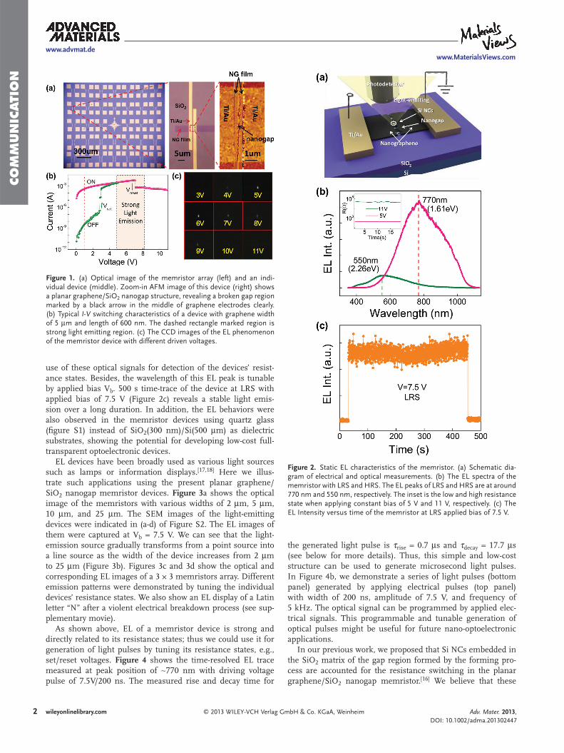
Figure 1 a shows the image of the as-made two-terminal memristor devices array. Atomic force microscopy (AFM) image of an individual device with width of 5 μ m and length of 600 nm after forming process reveals a planar memristor struc-ture with nanogapped graphene fi lm as electrodes and SiO 2 as conduction channel. Polycrystalline graphene fi lm was directly grown on SiO 2 substrates using a remote plasma assisted chem-ical vapor deposition techniques. Refer to our previous paper for the device fabrication process. [ 16 ] Resistances of this type of devices can be tuned from LRS (“ON”) to HRS (“OFF”) via set and reset voltages. Note that all electrical operation and meas-urements were carried out in vacuum of <2 × 10 −4 Torr at room temperature, and the optical measurements were performed in a dark room. The dc sweep I-V properties and constant bias were characterized by an Agilent 4156C semiconductor para-meter analyzer. Figure 1 b shows a typical I-V switching char-acteristic of a memristor device under dc voltage sweep. In the set process, the current jumps abruptly at V set = ∼ 3 V to ON state from OFF state. The device recovers to OFF state at V reset = ∼ 7 V when sweeping voltage from 0 to 11 V in the reset process. The ON/OFF ratio is ∼ 10 5 as marked by the vertical dashed line. During the electrical operation for a memristor device from LRS to HRS, strong light emission accompanying with the I-V switching process was observed, which was even visible by naked eyes. Figure 1 c illustrates the light emission at different resistance states as well as bias voltages (V b ) for the memristor devices, imaged by a charge coupled device (CCD) camera connected to a long focal distance microscope. We can see that the EL intensity increased with V b , reached maximum at 5–6 V, and gradually weakened at V b > 6 V.
The EL spectra were collected by spectrometer connected to a microscope through an optical fi ber, as illustrated in Figure 2 a. The EL spectra of the above-mentioned device at V b = 5 V (LRS) and V b = 11V (HRS) collected at an integration time of 5 s are shown in Figure 2 b. We can see that the light emission covers the entire visible light and near-infrared range of 400–1100 nm and shows a broadened peak centered at 770 nm and 550 nm for LRS and HRS, respectively. The dynamic characteristic of the EL was measured by monochromator targeting on the wave-length of 750 nm. The amplitude of LRS EL peak is an order of magnitude higher than that for HRS, indicating a potential DOI: 10.1002/adma.201302447
C. He, P. Chen, J. Zhao, M. Cheng, W. Yang, G. Xie, D. Wang, D. Liu, R. Yang, D. Shi, G. Zhang Nanoscale Physics and devices LaboratoryBeijing National Laboratory for Condensed Matter Physics and Institute of Physics Chinese Academy of Sciences , Beijing , 100190 , China E-mail: [email protected] J. Li, Z. LiLaboratory of Optical Physics Beijing National Laboratory for Condensed Matter Physics and Institute of Physics Chinese Academy of Sciences Beijing , 100190 , China X. Wu, K. Yin, L. SunSEU-FEI Nano-Pico CenterKey Laboratory of MEMS of Ministry of Education School of Electrical Science and Engineering Southeast University 210096 , Nanjing , China
Adv. Mater. 2013, DOI: 10.1002/adma.201302447
2
www.advmat.dewww.MaterialsViews.com
wileyonlinelibrary.com © 2013 WILEY-VCH Verlag GmbH & Co. KGaA, Weinheim
CO
MM
UN
ICATI
ON
use of these optical signals for detection of the devices’ resist-ance states. Besides, the wavelength of this EL peak is tunable by applied bias V b . 500 s time-trace of the device at LRS with applied bias of 7.5 V (Figure 2 c) reveals a stable light emis-sion over a long duration. In addition, the EL behaviors were also observed in the memristor devices using quartz glass (fi gure S1) instead of SiO 2 (300 nm)/Si(500 μ m) as dielectric substrates, showing the potential for developing low-cost full-transparent optoelectronic devices.
EL devices have been broadly used as various light sources such as lamps or information displays. [ 17,18 ] Here we illus-trate such applications using the present planar graphene/SiO 2 nanogap memristor devices. Figure 3 a shows the optical image of the memristors with various widths of 2 μ m, 5 μ m, 10 μ m, and 25 μ m. The SEM images of the light-emitting devices were indicated in (a-d) of Figure S2. The EL images of them were captured at V b = 7.5 V. We can see that the light-emission source gradually transforms from a point source into a line source as the width of the device increases from 2 μ m to 25 μ m (Figure 3 b). Figures 3 c and 3 d show the optical and corresponding EL images of a 3 × 3 memristors array. Different emission patterns were demonstrated by tuning the individual devices’ resistance states. We also show an EL display of a Latin letter “N” after a violent electrical breakdown process (see sup-plementary movie).
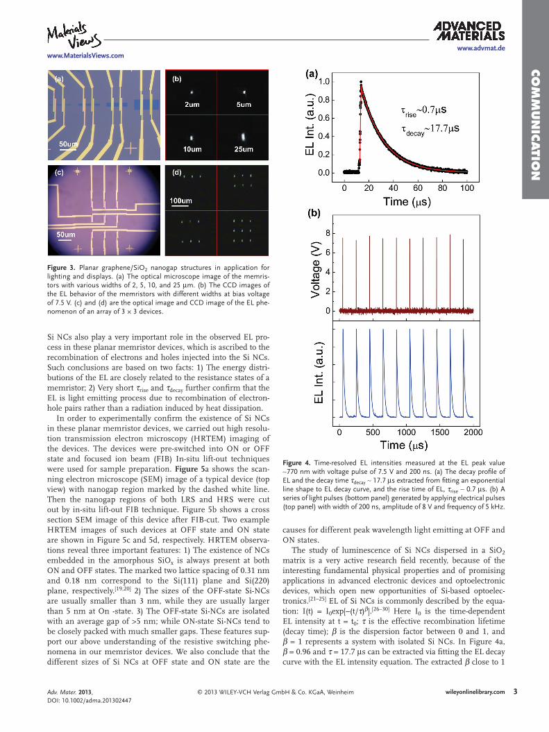
As shown above, EL of a memristor device is strong and directly related to its resistance states; thus we could use it for generation of light pulses by tuning its resistance states, e.g., set/reset voltages. Figure 4 shows the time-resolved EL trace measured at peak position of ∼ 770 nm with driving voltage pulse of 7.5V/200 ns. The measured rise and decay time for
the generated light pulse is τ rise = 0.7 μ s and τ decay = 17.7 μ s (see below for more details). Thus, this simple and low-cost structure can be used to generate microsecond light pulses. In Figure 4 b, we demonstrate a series of light pulses (bottom panel) generated by applying electrical pulses (top panel) with width of 200 ns, amplitude of 7.5 V, and frequency of 5 kHz. The optical signal can be programmed by applied elec-trical signals. This programmable and tunable generation of optical pulses might be useful for future nano-optoelectronic applications.
In our previous work, we proposed that Si NCs embedded in the SiO 2 matrix of the gap region formed by the forming pro-cess are accounted for the resistance switching in the planar graphene/SiO 2 nanogap memristor. [ 16 ] We believe that these
Figure 1. (a) Optical image of the memristor array (left) and an indi-vidual device (middle). Zoom-in AFM image of this device (right) shows a planar graphene/SiO 2 nanogap structure, revealing a broken gap region marked by a black arrow in the middle of graphene electrodes clearly. (b) Typical I-V switching characteristics of a device with graphene width of 5 μ m and length of 600 nm. The dashed rectangle marked region is strong light emitting region. (c) The CCD images of the EL phenomenon of the memristor device with different driven voltages.
Figure 2. Static EL characteristics of the memristor. (a) Schematic dia-gram of electrical and optical measurements. (b) The EL spectra of the memristor with LRS and HRS. The EL peaks of LRS and HRS are at around 770 nm and 550 nm, respectively. The inset is the low and high resistance state when applying constant bias of 5 V and 11 V, respectively. (c) The EL Intensity versus time of the memristor at LRS applied bias of 7.5 V.
Adv. Mater. 2013, DOI: 10.1002/adma.201302447
3
www.advmat.dewww.MaterialsViews.com
wileyonlinelibrary.com© 2013 WILEY-VCH Verlag GmbH & Co. KGaA, Weinheim
CO
MM
UN
ICATIO
N
causes for different peak wavelength light emitting at OFF and ON states.
The study of luminescence of Si NCs dispersed in a SiO 2 matrix is a very active research fi eld recently, because of the interesting fundamental physical properties and of promising applications in advanced electronic devices and optoelectronic devices, which open new opportunities of Si-based optoelec-tronics. [ 21–25 ] EL of Si NCs is commonly described by the equa-tion: I(t) = I 0 exp[–(t/ τ ) β ]. [ 26–30 ] Here I 0 is the time-dependent EL intensity at t = t 0 ; τ is the effective recombination lifetime (decay time); β is the dispersion factor between 0 and 1, and β = 1 represents a system with isolated Si NCs. In Figure 4 a, β = 0.96 and τ = 17.7 μ s can be extracted via fi tting the EL decay curve with the EL intensity equation. The extracted β close to 1
Si NCs also play a very important role in the observed EL pro-cess in these planar memristor devices, which is ascribed to the recombination of electrons and holes injected into the Si NCs. Such conclusions are based on two facts: 1) The energy distri-butions of the EL are closely related to the resistance states of a memristor; 2) Very short τ rise and τ decay further confi rm that the EL is light emitting process due to recombination of electron-hole pairs rather than a radiation induced by heat dissipation.
In order to experimentally confi rm the existence of Si NCs in these planar memristor devices, we carried out high resolu-tion transmission electron microscopy (HRTEM) imaging of the devices. The devices were pre-switched into ON or OFF state and focused ion beam (FIB) In-situ lift-out techniques were used for sample preparation. Figure 5 a shows the scan-ning electron microscope (SEM) image of a typical device (top view) with nanogap region marked by the dashed white line. Then the nanogap regions of both LRS and HRS were cut out by in-situ lift-out FIB technique. Figure 5 b shows a cross section SEM image of this device after FIB-cut. Two example HRTEM images of such devices at OFF state and ON state are shown in Figure 5 c and 5 d, respectively. HRTEM observa-tions reveal three important features: 1) The existence of NCs embedded in the amorphous SiO x is always present at both ON and OFF states. The marked two lattice spacing of 0.31 nm and 0.18 nm correspond to the Si(111) plane and Si(220) plane, respectively. [ 19,20 ] 2) The sizes of the OFF-state Si-NCs are usually smaller than 3 nm, while they are usually larger than 5 nm at On -state. 3) The OFF-state Si-NCs are isolated with an average gap of >5 nm; while ON-state Si-NCs tend to be closely packed with much smaller gaps. These features sup-port our above understanding of the resistive switching phe-nomena in our memristor devices. We also conclude that the different sizes of Si NCs at OFF state and ON state are the
Figure 3. Planar graphene/SiO 2 nanogap structures in application for lighting and displays. (a) The optical microscope image of the memris-tors with various widths of 2, 5, 10, and 25 μ m. (b) The CCD images of the EL behavior of the memristors with different widths at bias voltage of 7.5 V. (c) and (d) are the optical image and CCD image of the EL phe-nomenon of an array of 3 × 3 devices.
Figure 4. Time-resolved EL intensities measured at the EL peak value ∼ 770 nm with voltage pulse of 7.5 V and 200 ns. (a) The decay profi le of EL and the decay time τ decay ∼ 17.7 μ s extracted from fi tting an exponential line shape to EL decay curve, and the rise time of EL, τ rise ∼ 0.7 μ s. (b) A series of light pulses (bottom panel) generated by applying electrical pulses (top panel) with width of 200 ns, amplitude of 8 V and frequency of 5 kHz.
Adv. Mater. 2013, DOI: 10.1002/adma.201302447

4
www.advmat.dewww.MaterialsViews.com
wileyonlinelibrary.com © 2013 WILEY-VCH Verlag GmbH & Co. KGaA, Weinheim
CO
MM
UN
ICATI
ON
time constant is always <1 μ s, the decay time around ∼ 18.0 μ s, and the value of β is around 0.96–0.98.
Several models have been proposed to explain the lumines-cence in Si NCs, including quantum confi nement, [ 31,32 ] sur-face states, [ 33 ] and defects in the oxide. [ 34 ] For simplicity, here we only consider quantum confi nement effects. Resemble single exponential EL decay curves reveal that surface states
reveals that such a system behaves more like isolated crystals. This may be explained by that exciton diffusion in the system is very much suppressed due to the fast nonradiative recom-bination. The rise time constant τ rise of EL is ∼ 0.7 μ s. The rise time and decay time exhibited no obvious dependence on the driving pulse width and the detected wavelength (shown in Figure S3). We measured many devices and found that the rise
Figure 5. The EL mechanism in the planar graphene/SiO 2 nanogap structure memristor. Recombination of the electrons and holes injected into the Si NCs with in the nanogap results in the emission of light. HRTEM imaging of the devices were carried out to experimentally confi rm the existence of the Si NCs in these planar memristor devices (a–d). (a) The SEM image of the switching planar graphene/SiO 2 nanogap structure (top view). The dashed white line indicates the confi ned nanogap site, which location is the FIB-cut along with. (b) The side view SEM image of cross section cor-responding to the dashed white line in (a). HRTEM images of the nanogap region as indicated by white dashed rectangle in (b) with the devices at OFF state (c) and ON state (d). Nanocrystalline structures are delineated by white dashed lines. The lattice spacing of the NCs is either at 0.31 nm or at 0.18 nm, corresponding to that in a Si(111) plane and a Si(220) plane. The sizes of Si NCs of OFF state are usually smaller than 3 nm, whereas that of ON state are always greater than 5 nm. (e–f) are schematic diagram of the EL mechanism. The wavelength of the emission light is determined by the bandgap of the Si NCs, which depend on the size of the Si NCs cluster. The Si NCs in the nanogap of OFF state were shown in (e), the size of which are mostly distributed in 2 ∼ 3 nm deduced from the green EL spectra. (f) indicates the Si NCs in the nanogap of ON state, the size of which are mostly distributed in 4 ∼ 5 nm inferred from the red emission.
Adv. Mater. 2013, DOI: 10.1002/adma.201302447

5
www.advmat.dewww.MaterialsViews.com
wileyonlinelibrary.com© 2013 WILEY-VCH Verlag GmbH & Co. KGaA, Weinheim
CO
MM
UN
ICATIO
N
and defects have a negligible impact on the radiative recom-bination mechanism. Recombination of the electrons and holes injected into the isolated NCs results in the emission of light. Figure 5 e–f indicates the schematic diagram of the EL mechanism in a planar graphene/SiO 2 nanogap mem-ristor. The wavelength of the emission light depended on the bandgap of the NCs, which is determined by the size of the Si NCs. The broad EL spectrum (across the range from 400 to 1100 nm) refl ects the size distribution of Si NCs. The green EL spectra of HRS state and the red emission of LRS state illustrate the size dependence of Si NCs formed at LRS and HRS. Following the quantum confi nement model, the peak EL energy is equal to the free exciton band gap. This can be used to deduce the average size of the Si NCs in the nanogap of HRS and LRS states, which are most distributed around in 2 ∼ 3 nm and 4 ∼ 5 nm, [ 35–38 ] respectively, in consistence with our TEM results.
In conclusion, EL behaviors in planar graphene/SiO 2 nanogap memristors were observed. The EL spectra cover the wavelength range from 400 to 1100 nm. The EL behav-iors are attributed to recombination of the electrons and holes injected into the NCs located within the nanogap that is sub-ject to quantum confi nement effect. The EL peaks can be tuned between 550 nm and 770 nm reliably and controllably via setting the device to different resistance states, i.e., HRS and LRS, thus altering the size of the Si NCs in the device. The rise and decay time constant of the EL process were measured with τ rise = 0.7 μ s and τ decay = 17.7 μ s, respectively. The connection between device’s resistance states and EL can be used to identify each other. Our results point to the possi-bility of using this simple structure for creating light-emitting structures for optical communications photonic integrated circuits across the spectral region 400–1100 nm. In addition, the fabrication process of these light-emitting memristor is simple, low-cost, scalable and fully compatible with silicon-based technologies. The simple nanogap structure may be very important for future nanoelectronic and optoelectronic applications.
Experimental Section Imaging of the graphene/SiO 2 nanogap structures : An atomic force
microscope (Multi-Mode IIId, Veeco Instruments Inc.) was used for imaging the nanogap in the middle of the NG fi lm. The SEM images were obtained by the SEM mode of Raith e-line e-beam lithography system. For the HRTEM analysis, the TEM sample was prepared by focused ion beam (FIB) using a gallium beam in a dual beam Helios system from FEI. The device was switched ON or OFF state by dc voltage sweeping before FIB-cut. Then the nanogap regions of both LRS and HRS were cut out by in-situ lift-out FIB technique. Low-kV cleaning process was used to remove the surface amorphous layer. After TEM sample preparation, HRTEM was carried out using an image aberration-corrected TEM (FEI Titan 80–300) with an acceleration voltage of 30 kV.
Measurements of electrical characteristics of the devices : The dc sweep I-V properties and constant bias were characterized by an Agilent 4156C semiconductor parameter analyzer in vacuum of <2 × 10 −4 Torr at room temperature. Agilent 33250A pulse generator was used to measure the EL decay time and to generate the light pulse. The semiconductor parameter analyzer and the pulse generator were connected the vacuum chamber by using triax cables. The device was load onto a chip carrier inside the measurement vacuum chamber with the Ti/Au electrode pads
attached to the chip carrier through wire-bonding, which were connected to the atmosphere via a feed-through.
Characterization of the EL in the graphene/SiO 2 nanogap structure memristors : In our optical measurements, the light from the memristor was collected by a long focal distance microscope objective, imaged by a charge coupled device (CCD, HITACHI, KP-D20) camera connected to the microscope. The EL spectra were measured by using a spectrometer (Ocean Optics, QE6500) connected to the microscope through an optical fi ber. A monochromator (Zolix, Omni- λ 300) equipped with a fast photomultiplier tube (Hamamatsu, H7422P-50) and an oscilloscope (Agilent, DSOX3054A) were used to measure and record the dynamic characteristics of the EL behavior.
Supporting Information Supporting Information is available from the Wiley Online Library or from the author.
Acknowledgment G.Z. acknowledges fi nancial support from the National Basic Research Program of China (973 Program) under the grant No. 2013CB934500 and the National Science Foundation of China (NSFC) under the grant Nos. 91223204, 11204358, and 11174333. L.S. acknowledges fi nancial support from the 973 programs (2011CB707601, 2009CB623702) and Chinese postdoctoral funding (No. 2012M520053) and Jiangsu Province Funds for Distinguished Young Scientists (No. BK2012024).
Received: May 29, 2013 Revised: June 24, 2013
Published online:
[1] D. B. Strukov , G. S. Snider , D. R. Stewart , R. S. Williams , Nature 2008 , 453 , 80 .
[2] L. O. Chua , IEEE Transactions on Circuit Theory 1971 , CT18 , 507 . [3] J. J. Yang , M. D. Pickett , X. M. Li , D. A. A. Ohlberg , D. R. Stewart ,
R. S. Williams , Nat. Nanotechnol. 2008 , 3 , 429 . [4] H. Yenpo , G. M. Huang , L. Peng , Proc. 2009 IEEE/ACM ICCAD
2009 , 485 . [5] S. H. Jo , T. Chang , I. Ebong , B. B. Bhadviya , P. Mazumder , W. Lu ,
Nano Lett. 2010 , 10 , 1297 . [6] M. K. Hota , M. K. Bera , B. Kundu , S. C. Kundu , C. K. Maiti , Adv.
Funct. Mater. 2012 , 22 , 4493 . [7] B. Muthuswamy , P. P. Kokate , Memristor-Based Chaotic Circuits.
IETE Tech. Rev. 2009 , 26 , 417 . [8] W. H. Sun , C. F. Li , J. B. Yu , Ieee, A Memristor Based Chaotic Oscil-
lator , Ieee : New York , 2009 , 955 . [9] J. Borghetti , G. S. Snider , P. J. Kuekes , J. J. Yang , D. R. Stewart ,
R. S. Williams , Nature 2010 , 464 , 873 . [10] Y. Yilmaz , P. Mazumder , 2012 IEEE 12th Int. Conf. Nanotechnol.
2012 , 1 – 4 . [11] R. Waser , M. Aono , Nat. Mater. 2007 , 6 , 833 . [12] Y. B. L. Y. B. Li , A. Sinitskii , J. M. Tour , Nat. Mater. 2008 , 7 , 966 . [13] T. W. Hickmott , J. Vacuum Sci. Technol. 1969 , 6 , 828 . [14] S. F. Alvarado , F. La Mattina , J. G. Bednorz , Appl. Phys. a - Mater.
2007 , 89 , 85 . [15] A. A. Zakhidov , B. Jung , J. D. Slinker , H. D. Abruna , G. G. Malliaras ,
Org. Electron 2010 , 11 , 150 . [16] C. L. He , Z. W. Shi , L. C. Zhang , W. Yang , R. Yang , D. X. Shi ,
G. Y. Zhang , ACS Nano 2012 , 6 , 4214 . [17] R. H. Friend , R. W. Gymer , A. B. Holmes , J. H. Burroughes ,
R. N. Marks , C. Taliani , D. D. C. Bradley , D. A. Dos Santos ,
Adv. Mater. 2013, DOI: 10.1002/adma.201302447

6
www.advmat.dewww.MaterialsViews.com
wileyonlinelibrary.com © 2013 WILEY-VCH Verlag GmbH & Co. KGaA, Weinheim
CO
MM
UN
ICATI
ON [29] A. Irrera , D. Pacifi ci , M. Miritello , G. Franzo , F. Priolo , F. Iacona ,
D. Sanfi lippo , G. Di Stefano , P. G. Fallica , Appl. Phys. Lett. 2002 , 81 , 1866 .
[30] A. Anopchenko , A. Marconi , E. Moser , S. Prezioso , M. Wang , L. Pavesi , G. Pucker , P. Bellutti , J. Appl. Phys. Lett. 2009 , 106 , 033104 .
[31] P. K. Basu , Proceeding of the Tenth International Workshop on the Physics of Semiconductor Devices , Vols I and Ii , V. Kumar , S. K. Agarwal , Eds. Spie-Int Soc Optical Engineering : Bellingham , 2000 , 3975 , 937 .
[32] N. M. Park , T. S. Kim , S. J. Park , Appl. Phys. Lett. 2001 , 78 , 2575 . [33] F. Koch , V. Petrovakoch , T. Muschik , J. Lumines. 1993 , 57 , 271 . [34] S. M. Prokes , Appl. Phys. Lett. 1993 , 62 , 3244 . [35] J. P. Proot , C. Delerue , G. Allan , Appl. Phys. Lett. 1992 , 61 , 1948 . [36] M. V. Wolkin , J. Jorne , P. M. Fauchet , G. Allan , C. Delerue , Phys. Rev.
Lett. 1999 , 82 , 197 . [37] J. Heitmann , F. Muller , M. Zacharias , U. Gosele , Adv. Mater. 2005 ,
17 , 795 . [38] P. D. Nguyen , D. M. Kepaptsoglou , Q. M. Ramasse , A. Olsen , Phys.
Rev. B 2012 , 85 , 085315 .
J. L. Bredas , M. Logdlund , W. R. Salaneck , Nature 1999 , 397 , 121 .
[18] R. H. Kim , M. H. Bae , D. G. Kim , H. Y. Cheng , B. H. Kim , D. H. Kim , M. Li , J. Wu , F. Du , H. S. Kim , S. Kim , D. Estrada , S. W. Hong , Y. G. Huang , E. Pop , J. A. Rogers , Nano Lett. 2011 , 11 , 3881 .
[19] Y. Q. Wang , T. Li , W. S. Liang , X. F. Duan , G. G. Ross , Nanotech-nology 2009 , 20 , 315704 .
[20] J. Yao , Z. Z. Sun , L. Zhong , D. Natelson , J. M. Tour , Nano Lett. 2010 , 10 , 4105 .
[21] L. Pavesi , L. Dal Negro , C. Mazzoleni , G. Franzo , F. Priolo , Nature 2000 , 408 , 440 .
[22] J. Valenta , N. Lalic , J. Linnros , Appl. Phys. Lett. 2004 , 84 , 1459 . [23] R. J. Walters , G. I. Bourianoff , H. A. Atwater , Nat. Mater. 2005 , 4 , 143 . [24] P. M. Fauchet , Mater. Today 2005 , 8 , 26 . [25] V. Beyer , B. Schmidt , K. H. Heinig , K. H. Stegemann , Appl. Phys.
Lett. 2009 , 95 , 193501 . [26] Y. Kanemitsu , Phys. Rev. B 1994 , 49 , 16845 . [27] P. J. Ventura , M. C. Docarmo , K. P. Odonnell , J. Appl. Phys. 1995 , 77 , 323 . [28] J. Linnros , N. Lalic , A. Galeckas , V. Grivickas , J. Appl. Phys. 1999 , 86 ,
6128 .
Adv. Mater. 2013, DOI: 10.1002/adma.201302447