TUNABLE Au/Ga2S3/Yb VARACTOR DIODES DESIGNED ...
8
Chalcogenide Letters Vol. 14, No. 9, September 2017, p. 381 - 388 TUNABLE Au/Ga 2 S 3 /Yb VARACTOR DIODES DESIGNED FOR HIGH FREQUENCY APPLICATIONS S. E. AL GARNI a* , A. F. QASRAWI b a Physics Department, Faculty of Science- Al Faisaliah, King Abdulaziz University, Jeddah- Saudi Arabia b Departments of Physics at AAUP, Jenin and Group of physics, Faculty of Engineering, Atilim University, 06836 Ankara, Turkey In this work, the design and characterization of Au/Ga 2 S 3 /Yb Schottky barrier is investigated by means of transmittance electron microscopy (TEM), scanning electron microscopy (SEM), energy dispersive X-ray spectroscopy (EDXS), capacitance spectroscopy, capacitance (C)-voltage (V) characteristics and impedance spectroscopy techniques. The design of the energy band diagram of the amorphous Au/Ga 2 S 3 interface revealed a theoretical energy barrier height ( ) and built in voltage ( ) of 2.04 and 1.88 eV, respectively. Experimentally, the was observed to be sensitive to the applied signal frequency. In addition, the capacitance spectra which were studied in the range of 10-1800 MHz, revealed resonance and antiresonance biasing dependent signal oscillations associated with negative capacitance values. On the other hand, impedance spectroscopy analysis revealed band pass/reject filtering properties in all the studied frequency range. The device exhibited a return loss, voltage standing wave ratio and power efficiency of 16.7 dB, 1.3 and 98.3% at 1400 MHz, respectively. (Received June 28, 2017; Accepted September 8, 2017) Keyword: Thin films; Vapor deposition; Electron microscopy; X-ray diffraction; Dielectrics; Electrical properties 1. Introduction Ga 2 S 3 is a compound that recently reported to be have smart features for visible light, microwave and infrared technological applications [1-5]. This compound is found to exhibit a maximal transparency in the range of 0.48-22.5 . In that range of spectral response, owing its anisotropic properties, the Ga 2 S 3 is attractive for use in nonlinear optical applications [1]. In addition, the three dimensional Ga 2 S 3 is suggested as a competitor to the layered GaSe and its solid solutions which possess outstanding optical properties. Both compounds are candidates for THz applications [2, 3]. Moreover, the photoluminescence spectral studies have shown that there exist a defect (excited Ga vacancies) related red (1.62 eV) and green (2.24 eV) emission lines in the Ga 2 S 3 films [4]. The p-Ga 2 S 3 /n-GaAs heterojunction displayed a large on/off current ratio under a blue laser (405 nm, 3.0 mW) illumination nominating it as high-power laser radiation sensor [4]. On the other hand, earlier studies of the temperature dependent Electrical and photoelectrical properties of the p-Si/ n-(Ga 2 Se 3 -Ga 2 S 3 ) thin films heterojunctions have shown that, the photovoltaic device reveal an open-circuit voltage of 0.70 V, a short-circuit current density of 9.42 mA cm −2 and a power conversion efficiency of 5.20% [5]. In our previous work, we have investigated the dielectric dispersion properties of the Ga 2 S 3 thin films which are deposited onto glass substrates [3]. The modeling of the dielectric spectra for these films in the frequency range of 270–1,000 THz, using the modified Drude- Lorentz model for electron-plasmon interactions revealed electron bound plasma frequencies in the range of ~0.76–0.94 (GHz). The corresponding drift mobility of electrons in the terahertz oscillating incident electric field was found to be 7.91 (cm 2 /Vs). The values are motivating for employing the Ga 2 S 3 thin films as tunable capacitor capable of resonating electrical signals at high * Correspond author: [email protected]
-
Upload
khangminh22 -
Category
Documents
-
view
0 -
download
0
Transcript of TUNABLE Au/Ga2S3/Yb VARACTOR DIODES DESIGNED ...
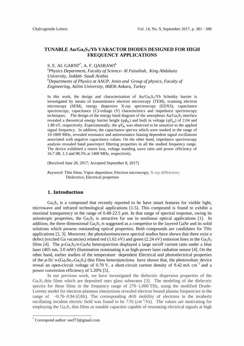
Chalcogenide Letters Vol. 14, No. 9, September 2017, p. 381 - 388
TUNABLE Au/Ga2S3/Yb VARACTOR DIODES DESIGNED FOR HIGH
FREQUENCY APPLICATIONS
S. E. AL GARNIa*
, A. F. QASRAWIb
aPhysics Department, Faculty of Science- Al Faisaliah, King Abdulaziz
University, Jeddah- Saudi Arabia bDepartments of Physics at AAUP, Jenin and
Group of physics, Faculty of
Engineering, Atilim University, 06836 Ankara, Turkey
In this work, the design and characterization of Au/Ga2S3/Yb Schottky barrier is
investigated by means of transmittance electron microscopy (TEM), scanning electron
microscopy (SEM), energy dispersive X-ray spectroscopy (EDXS), capacitance
spectroscopy, capacitance (C)-voltage (V) characteristics and impedance spectroscopy
techniques. The design of the energy band diagram of the amorphous Au/Ga2S3 interface
revealed a theoretical energy barrier height (𝑞𝜙𝑏) and built in voltage (𝑞𝑉𝑏𝑖) of 2.04 and
1.88 eV, respectively. Experimentally, the 𝑞𝑉𝑏𝑖 was observed to be sensitive to the applied
signal frequency. In addition, the capacitance spectra which were studied in the range of
10-1800 MHz, revealed resonance and antiresonance biasing dependent signal oscillations
associated with negative capacitance values. On the other hand, impedance spectroscopy
analysis revealed band pass/reject filtering properties in all the studied frequency range.
The device exhibited a return loss, voltage standing wave ratio and power efficiency of
16.7 dB, 1.3 and 98.3% at 1400 MHz, respectively.
(Received June 28, 2017; Accepted September 8, 2017)
Keyword: Thin films; Vapor deposition; Electron microscopy; X-ray diffraction; Dielectrics; Electrical properties
1. Introduction
Ga2S3 is a compound that recently reported to be have smart features for visible light,
microwave and infrared technological applications [1-5]. This compound is found to exhibit a
maximal transparency in the range of 0.48-22.5 𝜇𝑚. In that range of spectral response, owing its
anisotropic properties, the Ga2S3 is attractive for use in nonlinear optical applications [1]. In
addition, the three dimensional Ga2S3 is suggested as a competitor to the layered GaSe and its solid
solutions which possess outstanding optical properties. Both compounds are candidates for THz
applications [2, 3]. Moreover, the photoluminescence spectral studies have shown that there exist a
defect (excited Ga vacancies) related red (1.62 eV) and green (2.24 eV) emission lines in the Ga2S3
films [4]. The p-Ga2S3/n-GaAs heterojunction displayed a large on/off current ratio under a blue
laser (405 nm, 3.0 mW) illumination nominating it as high-power laser radiation sensor [4]. On the
other hand, earlier studies of the temperature dependent Electrical and photoelectrical properties
of the p-Si/ n-(Ga2Se3-Ga2S3) thin films heterojunctions have shown that, the photovoltaic device
reveal an open-circuit voltage of 0.70 V, a short-circuit current density of 9.42 mA cm−2
and a
power conversion efficiency of 5.20% [5].
In our previous work, we have investigated the dielectric dispersion properties of the
Ga2S3 thin films which are deposited onto glass substrates [3]. The modeling of the dielectric
spectra for these films in the frequency range of 270–1,000 THz, using the modified Drude-
Lorentz model for electron-plasmon interactions revealed electron bound plasma frequencies in the
range of ~0.76–0.94 (GHz). The corresponding drift mobility of electrons in the terahertz
oscillating incident electric field was found to be 7.91 (cm 2/Vs). The values are motivating for
employing the Ga2S3 thin films as tunable capacitor capable of resonating electrical signals at high
* Correspond author: [email protected]
382
frequencies. Thus, here in this work, we will discuss the design and characterization of the
Au/Ga2S3/Yb device as a promising circuit element. Particularly, we will explore the capacitance
spectra in the frequency range of 10-1800 MHz. In addition, the voltage biasing effect on the diode
performance will be studied and analyzed to determine the device operational parameters. The
frequency dependent voltage biasing of the Au/Ga2S3/Yb capacitors will be studied and analyzed
to determine the wave trapping features of the device.
2. Experimental details
Both of the Au, Yb and the Ga2S3 thin films were deposited using the vacuum evaporation
technique with the help of VCM600 thermal evaporator at a vacuum pressure of 10-5
mbar. Each
of the films was of 1.0 m thicknesses. The obtained Au films were used as substrates to
evaporate the Ga2S3. The X-ray diffraction patterns for the glass/ Ga2S3 and Au/Ga2S3 interface
were recorded using Rigako Utima IV X-ray diffraction unit. The surface morphology and
composition was studied using scanning electron microscopy with a JOEL JSM 7600F instrument
that has an energy dispersion X-ray spectrometer (EDXS). The transmittance electron microscopy
(JEOL JEM-1230) operating at 120 kV attached to a CCD camera was employed to reveals more
deep analysis of the Ga2S3 film properties. On the other hand, the electrical characterizations were
actualized with the help of an automated Keithley system that is equipped with a pico-ammeter
and voltage source. The impedance spectra were recorded using Agilent 4291B 10-1800 MHz
impedance analyzer.
3. Results and discussion
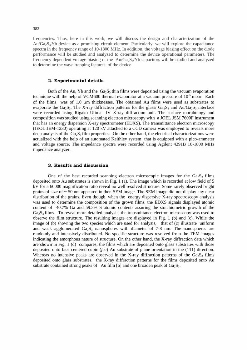
One of the best recorded scanning electron microscopic images for the Ga2S3 films
deposited onto Au substrates is shown in Fig. 1 (a). The image which is recorded at low field of 5
kV for a 60000 magnification ratio reveal no well resolved structure. Some rarely observed bright
grains of size of ~ 50 nm appeared in then SEM image. The SEM image did not display any clear
distribution of the grains. Even though, when the energy dispersive X-ray spectroscopy analysis
was used to determine the composition of the grown films, the EDXS signals displayed atomic
content of 40.7% Ga and 59.3% S atomic contents assuring the stoichiometric growth of the
Ga2S3 films. To reveal more detailed analysis, the transmittance electron microscopy was used to
observe the film structure. The resulting images are displayed in Fig. 1 (b) and (c). While the
image of (b) showing the two species which are used for analysis, that of (c) illustrate uniform
and weak agglomerated Ga2S3 nanospheres with diameter of 7-8 nm. The nanospheres are
randomly and intensively distributed. No specific structure was resolved from the TEM images
indicating the amorphous nature of structure. On the other hand, the X-ray diffraction data which
are shown in Fig. 1 (d) compares, the films which are deposited onto glass substrates with those
deposited onto face centered cubic (fcc) Au substrate of plane orientation in the (111) direction.
Whereas no intensive peaks are observed in the X-ray diffraction patterns of the Ga2S3 films
deposited onto glass substrates, the X-ray diffraction patterns for the films deposited onto Au
substrate contained strong peaks of Au film [6] and one broaden peak of Ga2S3.
383
Fig. 1 (a) The SEM images for a magnification of 60,000 , (b) The TEM image for a
50,000 and (c) for 200,000 times, and (d) the X-ray diffraction patterns for Ga2S3 films.
The Ga2S3 compound is known to exhibits monoclinic, hexagonal and cubic crystal
phases that appears at the same angles in the X-ray diffraction curves [4, 7]. Such a property
appears as a result of the existence of the small distortions in the lattice structures between the
hexagonal and the monoclinic Ga2S3 [4].The significant difference between them appears in the
change of the value of the relative intensity of the diffraction peaks as observed for Ga2S3
deposited onto GaAs substrates [4]. Since this type of crystallization is dominated by high
vacancy disorder and because Ga2S3 is a naturally defective semiconductor with one-third of
cation sites being vacant (Ga vacancies) [4], it easily forms an interfacial disorder of metal
atoms in some specific interfaces as observed in our structural and morphological analysis.
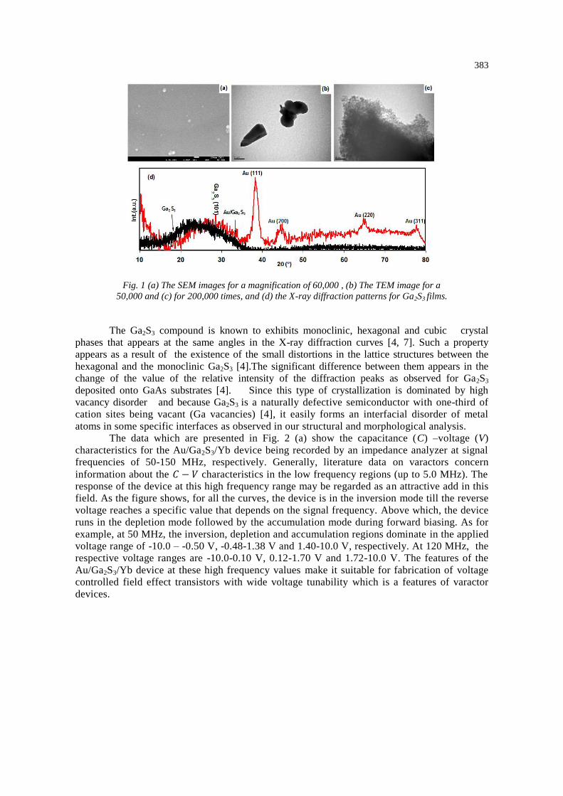
The data which are presented in Fig. 2 (a) show the capacitance (C) –voltage (V)
characteristics for the Au/Ga2S3/Yb device being recorded by an impedance analyzer at signal
frequencies of 50-150 MHz, respectively. Generally, literature data on varactors concern
information about the 𝐶 − 𝑉 characteristics in the low frequency regions (up to 5.0 MHz). The
response of the device at this high frequency range may be regarded as an attractive add in this
field. As the figure shows, for all the curves, the device is in the inversion mode till the reverse
voltage reaches a specific value that depends on the signal frequency. Above which, the device
runs in the depletion mode followed by the accumulation mode during forward biasing. As for
example, at 50 MHz, the inversion, depletion and accumulation regions dominate in the applied
voltage range of -10.0 – -0.50 V, -0.48-1.38 V and 1.40-10.0 V, respectively. At 120 MHz, the
respective voltage ranges are -10.0-0.10 V, 0.12-1.70 V and 1.72-10.0 V. The features of the
Au/Ga2S3/Yb device at these high frequency values make it suitable for fabrication of voltage
controlled field effect transistors with wide voltage tunability which is a features of varactor
devices.
384
Fig. 2 (a) The capacitance-voltage characteristics and (b) the 𝐶−2 − 𝑉 dependence for the
Au/Ga2S3/Yb diodes.
Physically, at a particular frequency, the behavior of the 𝐶 − 𝑉 characteristics which is
observed in Fig. 2 (a) can be explained as follows; for the n-type Ga2S3 increasing the values of
the positive voltage, causes band bending downward. This makes the edge of the conduction
band (𝐸𝑐) closer to the Fermi level (𝐸𝐹) at the surface and an accumulation of electrons is
obtained at the surface. On the other hand, negative values of applied voltages indicate an
upward bending of the bands which increase the distance from the 𝐸𝐹 to the bottom of the 𝐸𝑐
that in turn leads to a depletion of electrons at the surface of n-type Ga2S3 film. Increasing the
surface band bending to a value greater than the built in voltage of the Schottky device (𝑉𝑏𝑖)
brings the intrinsic level at the surface above the Fermi level and the density of minority
carriers (holes) become larger than intrinsic carrier density in the region just below the surface.
As the applied reverse voltage reaches a value of ~2𝑉𝑏𝑖, the density of holes increases and at
the top of the surface, the type of mobile carriers is inverted with respect to the bulk [8, 9].
In the depletion region, the capacitance voltage characteristic curves are analyzed in
accordance with the equation, 𝐶−2 = 2 (𝑉𝑏𝑖 − 𝑉 −𝑘𝑇
𝑞) /(𝑞𝜀𝑠𝐴2𝑁𝑑) [8]. The plots of the
𝐶−2 − 𝑉 dependence which are shown in Fig. 2 (b), reveal straight lines with slopes and
intercepts that in turn allow determining the density of uncompensated donors (𝑁𝑑) and the
built in voltage as well. The semiconductor (Ga2S3) dielectric constant (𝜀𝑠 ) and diode area are
substituted as 7.5 [3] and 3.14× 10⁻³ cm2, respectively. The resulting physical parameters of
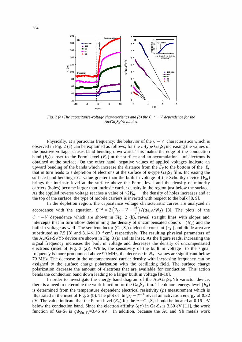
the Au/Ga2S3/Yb device are shown in Fig. 3 (a) and its inset. As the figure reads, increasing the
signal frequency increases the built in voltage and decreases the density of uncompensated
electrons (inset of Fig. 3 (a)). While, the sensitivity of the built in voltage to the signal
frequency is more pronounced above 90 MHz, the decrease in 𝑁𝑑 values are significant below
70 MHz. The decrease in the uncompensated carrier density with increasing frequency can be
assigned to the surface charge polarization with the oscillating field. The surface charge
polarization decrease the amount of electrons that are available for conduction. This action
bends the conduction band down leading to a larger built in voltage [8-10].
In order to investigate the energy band diagram of the Au/Ga2S3/Yb varactor device,
there is a need to determine the work function for the Ga2S3 film. The donors energy level (𝐸𝑑)
is determined from the temperature dependent electrical resistivity () measurement which is
illustrated in the inset of Fig. 2 (b). The plot of ln(𝜌) − 𝑇−1 reveal an activation energy of 0.32
eV. The value indicate that the Fermi level (𝐸𝐹) for the 𝑛 −Ga2S3 should be located at 0.16 eV
below the conduction band. Since the electron affinity (𝑞𝜒) in Ga2S3 is 3.30 eV [11], the work
function of Ga2S3 is 𝑞𝜙𝐺𝑎2𝑆3=3.46 eV. In addition, because the Au and Yb metals work
20
40
60
80
100
120
140
160
180
200
-10 -5 0 5 10
V (V)
C (
pF
)
150 MHz
120
80
60
50
0
1
2
3
4
5
6
7
8
9
0 1 2 3
V (V)
C-2
(x
10
20 F
-2)
150 MHz
120
80
60
50
Inversion
Dep
letio
n
Accumulation(a) (b)
14
15
16
17
2.4 2.6 2.8 3 3.2 3.41000/T (K
-1)
ln( r
(W
cm
)) Ed = 0.33 eV
385
functions (𝑞𝜙𝑚) are 5.34 and 2.51 eV [12], then, the Au and Yb contact metals represent a
Schottky (𝑞𝜙𝐴𝑢 > 𝑞𝜙𝐺𝑎2𝑆3) and Ohmic natures of contact, respectively. Thus, the theoretical
Schottky barrier height to the electrons motion for this device is ( 𝑞𝜙𝑏 = 𝑞𝜙𝐴𝑢 − 𝑞𝜒 ) 2.04
eV. The built in voltage (𝑞𝑉𝑏𝑖 = 𝑞𝜙𝐴𝑢 − 𝑞𝜙𝐺𝑎2𝑆3) is 1.88 eV. The energy band diagram for this
device is presented in Fig. 3 (b). The value of the built in voltage coincides with the
experimentally determined one (Fig. 3 (a)) at 120 MHz. The deviation of the 𝑞𝑉𝑏𝑖 from this
value at lower frequencies is ascribed to the degree of polarization (inability of charge carriers
to follow up with the field direction).
Fig. 3 (a) The frequency dependence of the built in voltage and (b) the energy band
diagram for the Au/Ga2S3/Yb diodes. The inset of (a) display the frequency dependence
of the density of uncompensated carriers.
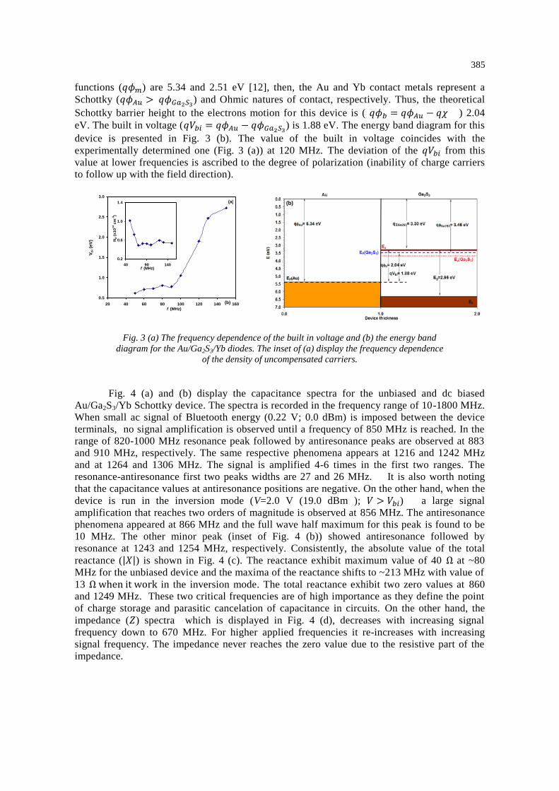
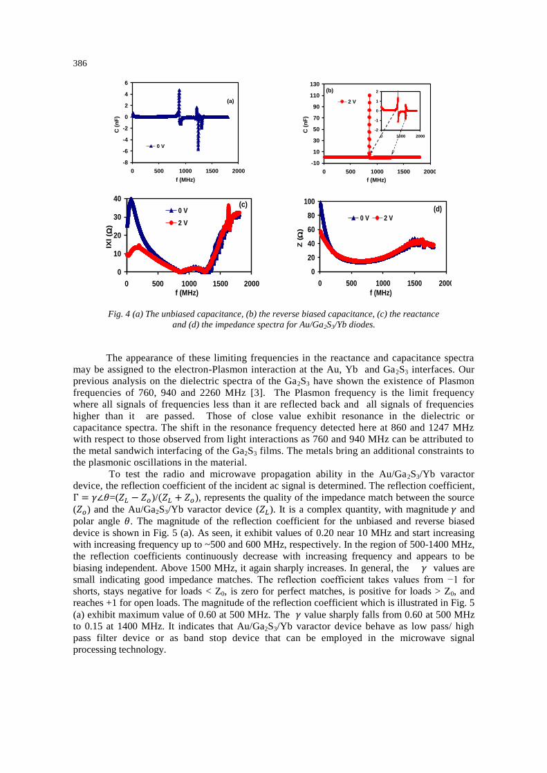
Fig. 4 (a) and (b) display the capacitance spectra for the unbiased and dc biased
Au/Ga2S3/Yb Schottky device. The spectra is recorded in the frequency range of 10-1800 MHz.
When small ac signal of Bluetooth energy (0.22 V; 0.0 dBm) is imposed between the device
terminals, no signal amplification is observed until a frequency of 850 MHz is reached. In the
range of 820-1000 MHz resonance peak followed by antiresonance peaks are observed at 883
and 910 MHz, respectively. The same respective phenomena appears at 1216 and 1242 MHz
and at 1264 and 1306 MHz. The signal is amplified 4-6 times in the first two ranges. The
resonance-antiresonance first two peaks widths are 27 and 26 MHz. It is also worth noting
that the capacitance values at antiresonance positions are negative. On the other hand, when the
device is run in the inversion mode (V=2.0 V (19.0 dBm ); 𝑉 > 𝑉𝑏𝑖) a large signal
amplification that reaches two orders of magnitude is observed at 856 MHz. The antiresonance
phenomena appeared at 866 MHz and the full wave half maximum for this peak is found to be
10 MHz. The other minor peak (inset of Fig. 4 (b)) showed antiresonance followed by
resonance at 1243 and 1254 MHz, respectively. Consistently, the absolute value of the total
reactance (|𝑋|) is shown in Fig. 4 (c). The reactance exhibit maximum value of 40 Ω at ~80
MHz for the unbiased device and the maxima of the reactance shifts to ~213 MHz with value of
13 Ω when it work in the inversion mode. The total reactance exhibit two zero values at 860
and 1249 MHz. These two critical frequencies are of high importance as they define the point
of charge storage and parasitic cancelation of capacitance in circuits. On the other hand, the
impedance (𝑍) spectra which is displayed in Fig. 4 (d), decreases with increasing signal
frequency down to 670 MHz. For higher applied frequencies it re-increases with increasing
signal frequency. The impedance never reaches the zero value due to the resistive part of the
impedance.
0.5
1.0
1.5
2.0
2.5
3.0
20 40 60 80 100 120 140 160f (MHz)
Vb
i (eV
)
0.2
0.6
1.0
1.4
40 90 140f (MHz)
Nd (
x1
014 c
m-3
)
(a)
(b)
(b)
0.5
1.0
1.5
2.0
2.5
3.0
20 40 60 80 100 120 140 160f (MHz)
Vb
i (eV
)
0.2
0.6
1.0
1.4
40 90 140f (MHz)
Nd (
x1
014 c
m-3
)
(a)
(b)
(b)
386
Fig. 4 (a) The unbiased capacitance, (b) the reverse biased capacitance, (c) the reactance
and (d) the impedance spectra for Au/Ga2S3/Yb diodes.
The appearance of these limiting frequencies in the reactance and capacitance spectra
may be assigned to the electron-Plasmon interaction at the Au, Yb and Ga2S3 interfaces. Our
previous analysis on the dielectric spectra of the Ga2S3 have shown the existence of Plasmon
frequencies of 760, 940 and 2260 MHz [3]. The Plasmon frequency is the limit frequency
where all signals of frequencies less than it are reflected back and all signals of frequencies
higher than it are passed. Those of close value exhibit resonance in the dielectric or
capacitance spectra. The shift in the resonance frequency detected here at 860 and 1247 MHz
with respect to those observed from light interactions as 760 and 940 MHz can be attributed to
the metal sandwich interfacing of the Ga2S3 films. The metals bring an additional constraints to
the plasmonic oscillations in the material.
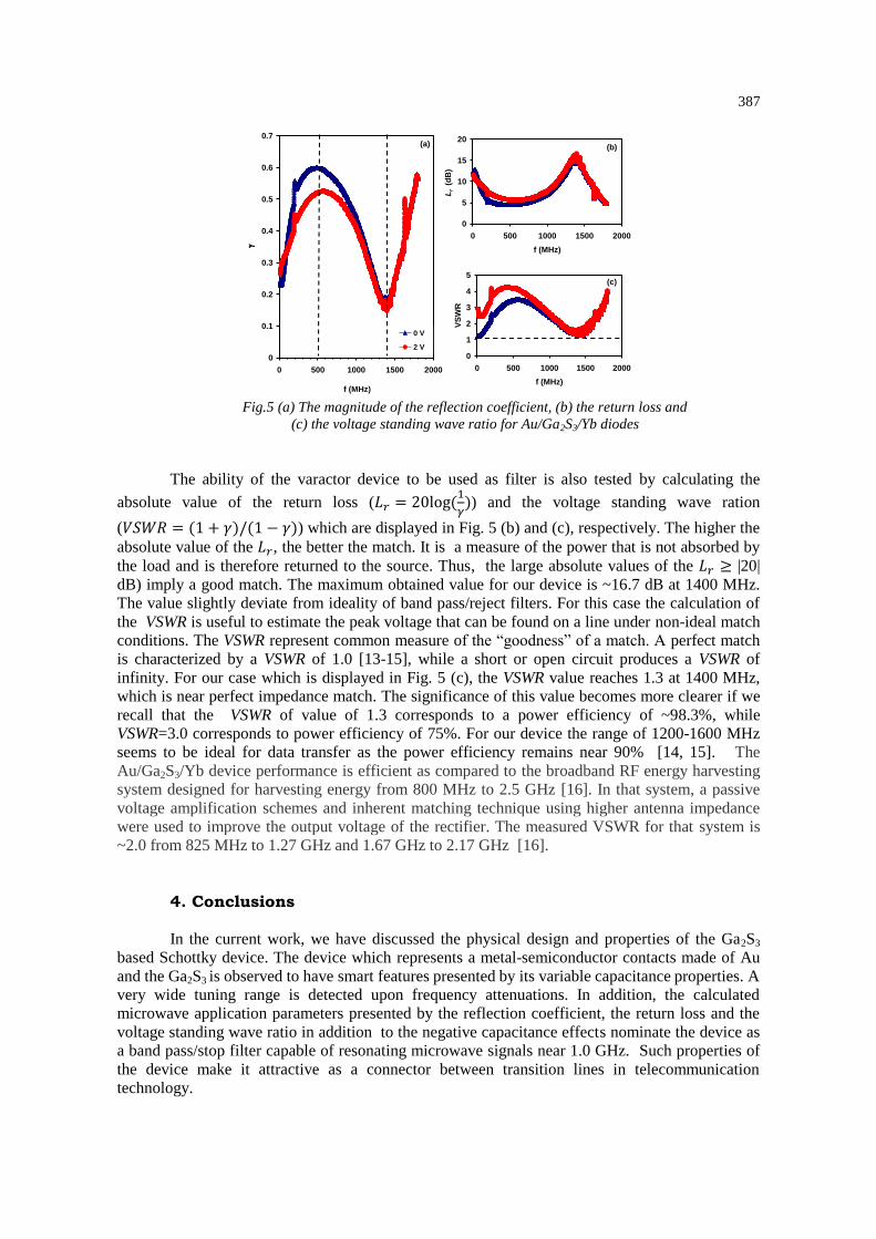
To test the radio and microwave propagation ability in the Au/Ga2S3/Yb varactor
device, the reflection coefficient of the incident ac signal is determined. The reflection coefficient,
Γ = 𝛾∠𝜃=(𝑍𝐿 − 𝑍𝑜)/(𝑍𝐿 + 𝑍𝑜), represents the quality of the impedance match between the source
(𝑍𝑜) and the Au/Ga2S3/Yb varactor device (𝑍𝐿). It is a complex quantity, with magnitude 𝛾 and
polar angle 𝜃. The magnitude of the reflection coefficient for the unbiased and reverse biased
device is shown in Fig. 5 (a). As seen, it exhibit values of 0.20 near 10 MHz and start increasing
with increasing frequency up to ~500 and 600 MHz, respectively. In the region of 500-1400 MHz,
the reflection coefficients continuously decrease with increasing frequency and appears to be
biasing independent. Above 1500 MHz, it again sharply increases. In general, the 𝛾 values are
small indicating good impedance matches. The reflection coefficient takes values from −1 for
shorts, stays negative for loads < Z0, is zero for perfect matches, is positive for loads > Z0, and
reaches +1 for open loads. The magnitude of the reflection coefficient which is illustrated in Fig. 5
(a) exhibit maximum value of 0.60 at 500 MHz. The 𝛾 value sharply falls from 0.60 at 500 MHz
to 0.15 at 1400 MHz. It indicates that Au/Ga2S3/Yb varactor device behave as low pass/ high
pass filter device or as band stop device that can be employed in the microwave signal
processing technology.
-10
10
30
50
70
90
110
130
0 500 1000 1500 2000
f (MHz)
C (
nF
)
2 V
0
10
20
30
40
0 500 1000 1500 2000f (MHz)
lXl
( W)
0 V
2 V
-8
-6
-4
-2
0
2
4
6
0 500 1000 1500 2000
f (MHz)
C (
nF
)
0 V
0
20
40
60
80
100
0 500 1000 1500 2000
f (MHz)
Z (
W)
0 V 2 V
(a)
(b)
(c)(d)
-2
-1
0
1
2
0 1000 2000
-10
10
30
50
70
90
110
130
0 500 1000 1500 2000
f (MHz)
C (
nF
)
2 V
0
10
20
30
40
0 500 1000 1500 2000f (MHz)
lXl
( W)
0 V
2 V
-8
-6
-4
-2
0
2
4
6
0 500 1000 1500 2000
f (MHz)
C (
nF
)
0 V
0
20
40
60
80
100
0 500 1000 1500 2000
f (MHz)
Z (
W)
0 V 2 V
(a)
(b)
(c)(d)
-2
-1
0
1
2
0 1000 2000
-10
10
30
50
70
90
110
130
0 500 1000 1500 2000
f (MHz)
C (
nF
)
2 V
0
10
20
30
40
0 500 1000 1500 2000f (MHz)
lXl
( W)
0 V
2 V
-8
-6
-4
-2
0
2
4
6
0 500 1000 1500 2000
f (MHz)
C (
nF
)
0 V
0
20
40
60
80
100
0 500 1000 1500 2000
f (MHz)
Z (
W)
0 V 2 V
(a)
(b)
(c)(d)
-2
-1
0
1
2
0 1000 2000
-10
10
30
50
70
90
110
130
0 500 1000 1500 2000
f (MHz)
C (
nF
)
2 V
0
10
20
30
40
0 500 1000 1500 2000f (MHz)
lXl
( W)
0 V
2 V
-8
-6
-4
-2
0
2
4
6
0 500 1000 1500 2000
f (MHz)
C (
nF
)0 V
0
20
40
60
80
100
0 500 1000 1500 2000
f (MHz)Z
(W
)
0 V 2 V
(a)
(b)
(c)(d)
-2
-1
0
1
2
0 1000 2000
387
Fig.5 (a) The magnitude of the reflection coefficient, (b) the return loss and
(c) the voltage standing wave ratio for Au/Ga2S3/Yb diodes
The ability of the varactor device to be used as filter is also tested by calculating the
absolute value of the return loss (𝐿𝑟 = 20log (1
𝛾)) and the voltage standing wave ration
(𝑉𝑆𝑊𝑅 = (1 + 𝛾)/(1 − 𝛾)) which are displayed in Fig. 5 (b) and (c), respectively. The higher the
absolute value of the 𝐿𝑟, the better the match. It is a measure of the power that is not absorbed by
the load and is therefore returned to the source. Thus, the large absolute values of the 𝐿𝑟 ≥ |20|
dB) imply a good match. The maximum obtained value for our device is ~16.7 dB at 1400 MHz.
The value slightly deviate from ideality of band pass/reject filters. For this case the calculation of
the VSWR is useful to estimate the peak voltage that can be found on a line under non-ideal match
conditions. The VSWR represent common measure of the “goodness” of a match. A perfect match
is characterized by a VSWR of 1.0 [13-15], while a short or open circuit produces a VSWR of
infinity. For our case which is displayed in Fig. 5 (c), the VSWR value reaches 1.3 at 1400 MHz,
which is near perfect impedance match. The significance of this value becomes more clearer if we
recall that the VSWR of value of 1.3 corresponds to a power efficiency of ~98.3%, while
VSWR=3.0 corresponds to power efficiency of 75%. For our device the range of 1200-1600 MHz
seems to be ideal for data transfer as the power efficiency remains near 90% [14, 15]. The
Au/Ga2S3/Yb device performance is efficient as compared to the broadband RF energy harvesting
system designed for harvesting energy from 800 MHz to 2.5 GHz [16]. In that system, a passive
voltage amplification schemes and inherent matching technique using higher antenna impedance
were used to improve the output voltage of the rectifier. The measured VSWR for that system is
~2.0 from 825 MHz to 1.27 GHz and 1.67 GHz to 2.17 GHz [16].
4. Conclusions
In the current work, we have discussed the physical design and properties of the Ga2S3
based Schottky device. The device which represents a metal-semiconductor contacts made of Au
and the Ga2S3 is observed to have smart features presented by its variable capacitance properties. A
very wide tuning range is detected upon frequency attenuations. In addition, the calculated
microwave application parameters presented by the reflection coefficient, the return loss and the
voltage standing wave ratio in addition to the negative capacitance effects nominate the device as
a band pass/stop filter capable of resonating microwave signals near 1.0 GHz. Such properties of
the device make it attractive as a connector between transition lines in telecommunication
technology.
0
0.1
0.2
0.3
0.4
0.5
0.6
0.7
0 500 1000 1500 2000
f (MHz)
g
0 V
2 V
0
5
10
15
20
0 500 1000 1500 2000
f (MHz)
Lr
(dB
)
0
1
2
3
4
5
0 500 1000 1500 2000
f (MHz)
VS
WR
(a) (b)
(c)
388
Acknowledgments
This article was funded by the Deanship of Scientific Research (DSR) at King Abdulaziz
University, Jeddah. The authors, therefore, acknowledge with thanks DSR for technical and
financial support.
References
[1] K. Konstantin, L. Ivan, S. Valery, G. Perizat, B.Askar, A. Yuri, Key Engineering Materials,
683(3), 71 (2016).
[2] Z. Huang, J-G. Huang, K. A. Kokh, V. A. Svetlichnyi, A. V. Shabalina, Yu M. Andreev,
G. V. Lanskii, 40th International Conference on Infrared, Millimeter, and Terahertz waves
(IRMMW-THz), IEEE, Chinese Univ Hong Kong, Hong Kong, PEOPLES R CHINA, pp. 1-2, August 2015.
[3] S. R. Alharbi, and A. F. Qasrawi, Plasmonics (2016). DOI: 10.1007/s11468-016-0357-4
[4] H. F. Liu, K.K A. Antwi, N. L. Yakovlev, H. R. Tan, L. T. Ong, S. J. Chua, D. Z. Chi, ACS
applied materials & interfaces 6(5), 3501 (2014).
[5] K. F. Abd. El-Rahman, The European Physical Journal Applied Physics 37(2), 143 (2007).
[6] C. A. Lucas, F. Maroun, N. Sisson, P. Thompson, Y. Grunder, R. Cortès, Ph. Allongue, The
Journal of Physical Chemistry C 120(6), 3360 (2016).
[7] O. Madelung, Semiconductors: data handbook. (Springer Science & Business Media,
New York, USA, 2012.
[8] W. Mönch, Semiconductor surfaces and interfaces, Springer, New York, USA, 2013.
[9] K. V. Reich, M. Schecter, and B. I. Shklovskii, Physical Review B 91(11), 115303 (2015).
[10] A. F. Qasrawi, Physica Scripta 89(6), 065802 (2014).
[11] N. Seeburrun, E. F. Archibong and P. Ramasami, Chemical Physics Letters 467(1), 23 (2008).
[12] H. L. Skriver, N. M. Rosengaard, Physical Review B 46(11), 7157 (1992).
[13] J. F. White, High frequency techniques: an introduction to RF and microwave engineering,
John Wiley & Sons, New York, USA, 2004.
[14] Y. Arbaoui, V. Laur, A. Maalouf, P. Quéffélec, D. Passerieux, A. Delias, P. Blondy, IEEE
Transactions on Microwave Theory and Techniques 64(1), 271 (2016).
[15] R. G. M. Oliveira, D. B. Freitas, M. C. Romeu, M. A. S. Silva, A. J. M. Sales, A. C. Ferreira,
A. S. B. Sombra, Microwave and Optical Technology Letters 58(5), 1211 (2016).
[16] M. Arrawatia, M. Sh. Baghini, G. Kumar, In 2016 IEEE MTT-S International Microwave
Symposium (IMS), pp. 1-3. IEEE, 345 E 47TH ST, NEW YORK, NY 10017 USA,
May 2016.


![Electronic spectra of Yb[sup 2+]-doped SrCl[sub 2]](https://static.fdokumen.com/doc/165x107/633592f8b5f91cb18a0b76fc/electronic-spectra-of-ybsup-2-doped-srclsub-2.jpg)