BZX384 series Voltage regulator diodes
11
DATA SHEET Product data sheet Supersedes data of 2003 Apr 01 2004 Mar 22 DISCRETE SEMICONDUCTORS BZX384 series Voltage regulator diodes
-
Upload
khangminh22 -
Category
Documents
-
view
5 -
download
0
Transcript of BZX384 series Voltage regulator diodes
DATA SHEET
Product data sheet Supersedes data of 2003 Apr 01
2004 Mar 22
DISCRETE SEMICONDUCTORS
BZX384 seriesVoltage regulator diodes
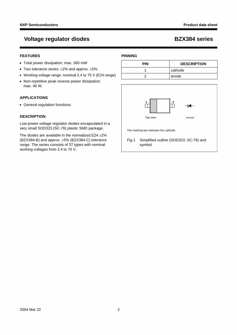
NXP Semiconductors Product data sheet
Voltage regulator diodes BZX384 series
FEATURES
• Total power dissipation: max. 300 mW• Two tolerance series: ±2% and approx. ±5%• Working voltage range: nominal 2.4 to 75 V (E24 range)• Non-repetitive peak reverse power dissipation:
max. 40 W.
APPLICATIONS
• General regulation functions.
DESCRIPTION
Low-power voltage regulator diodes encapsulated in a very small SOD323 (SC-76) plastic SMD package.
The diodes are available in the normalized E24 ±2% (BZX384-B) and approx. ±5% (BZX384-C) tolerance range. The series consists of 37 types with nominal working voltages from 2.4 to 75 V.
PINNING
PIN DESCRIPTION1 cathode2 anode
Fig.1 Simplified outline (SOD323; SC-76) and symbol.
handbook, halfpage
��1 2
Top view MAM387
The marking bar indicates the cathode.
2004 Mar 22 2
NXP Semiconductors Product data sheet
Voltage regulator diodes BZX384 series
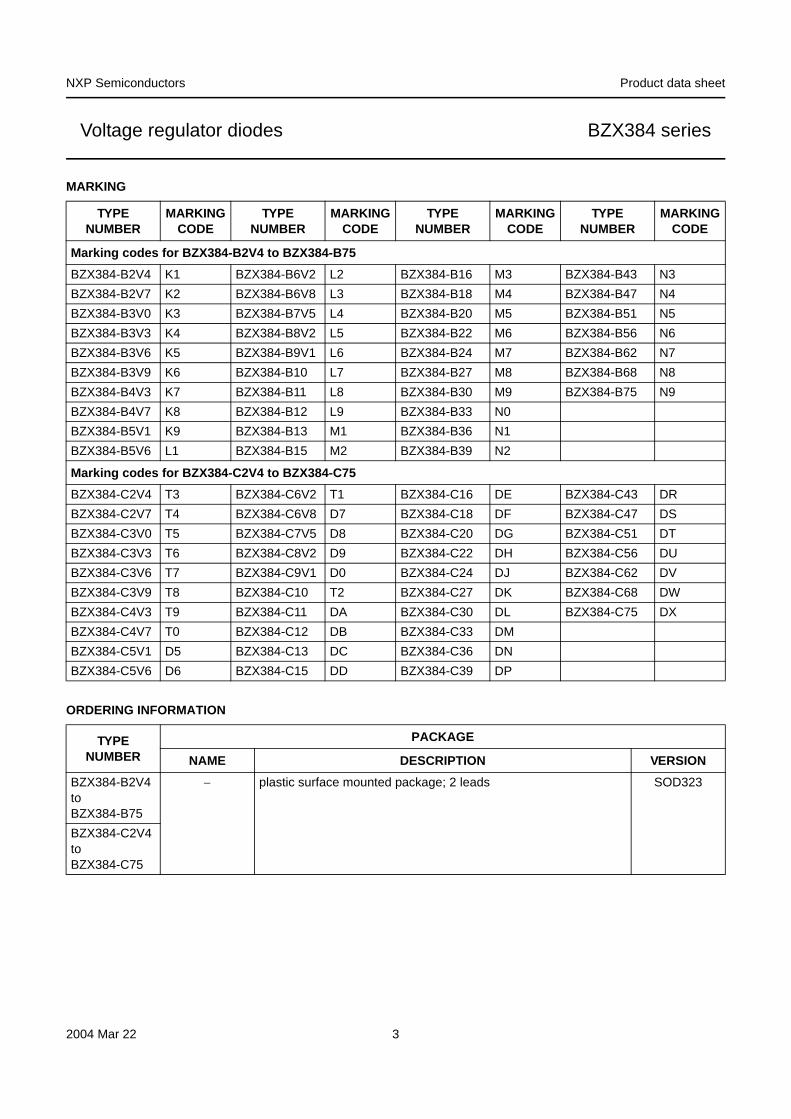
MARKING
ORDERING INFORMATION
TYPE NUMBER
MARKING CODE
TYPE NUMBER
MARKING CODE
TYPE NUMBER
MARKING CODE
TYPE NUMBER
MARKING CODE
Marking codes for BZX384-B2V4 to BZX384-B75BZX384-B2V4 K1 BZX384-B6V2 L2 BZX384-B16 M3 BZX384-B43 N3BZX384-B2V7 K2 BZX384-B6V8 L3 BZX384-B18 M4 BZX384-B47 N4BZX384-B3V0 K3 BZX384-B7V5 L4 BZX384-B20 M5 BZX384-B51 N5BZX384-B3V3 K4 BZX384-B8V2 L5 BZX384-B22 M6 BZX384-B56 N6BZX384-B3V6 K5 BZX384-B9V1 L6 BZX384-B24 M7 BZX384-B62 N7BZX384-B3V9 K6 BZX384-B10 L7 BZX384-B27 M8 BZX384-B68 N8BZX384-B4V3 K7 BZX384-B11 L8 BZX384-B30 M9 BZX384-B75 N9BZX384-B4V7 K8 BZX384-B12 L9 BZX384-B33 N0BZX384-B5V1 K9 BZX384-B13 M1 BZX384-B36 N1BZX384-B5V6 L1 BZX384-B15 M2 BZX384-B39 N2
Marking codes for BZX384-C2V4 to BZX384-C75BZX384-C2V4 T3 BZX384-C6V2 T1 BZX384-C16 DE BZX384-C43 DRBZX384-C2V7 T4 BZX384-C6V8 D7 BZX384-C18 DF BZX384-C47 DSBZX384-C3V0 T5 BZX384-C7V5 D8 BZX384-C20 DG BZX384-C51 DTBZX384-C3V3 T6 BZX384-C8V2 D9 BZX384-C22 DH BZX384-C56 DUBZX384-C3V6 T7 BZX384-C9V1 D0 BZX384-C24 DJ BZX384-C62 DVBZX384-C3V9 T8 BZX384-C10 T2 BZX384-C27 DK BZX384-C68 DWBZX384-C4V3 T9 BZX384-C11 DA BZX384-C30 DL BZX384-C75 DXBZX384-C4V7 T0 BZX384-C12 DB BZX384-C33 DMBZX384-C5V1 D5 BZX384-C13 DC BZX384-C36 DNBZX384-C5V6 D6 BZX384-C15 DD BZX384-C39 DP
TYPE NUMBER
PACKAGE
NAME DESCRIPTION VERSIONBZX384-B2V4 to BZX384-B75
− plastic surface mounted package; 2 leads SOD323
BZX384-C2V4 to BZX384-C75
2004 Mar 22 3
NXP Semiconductors Product data sheet
Voltage regulator diodes BZX384 series
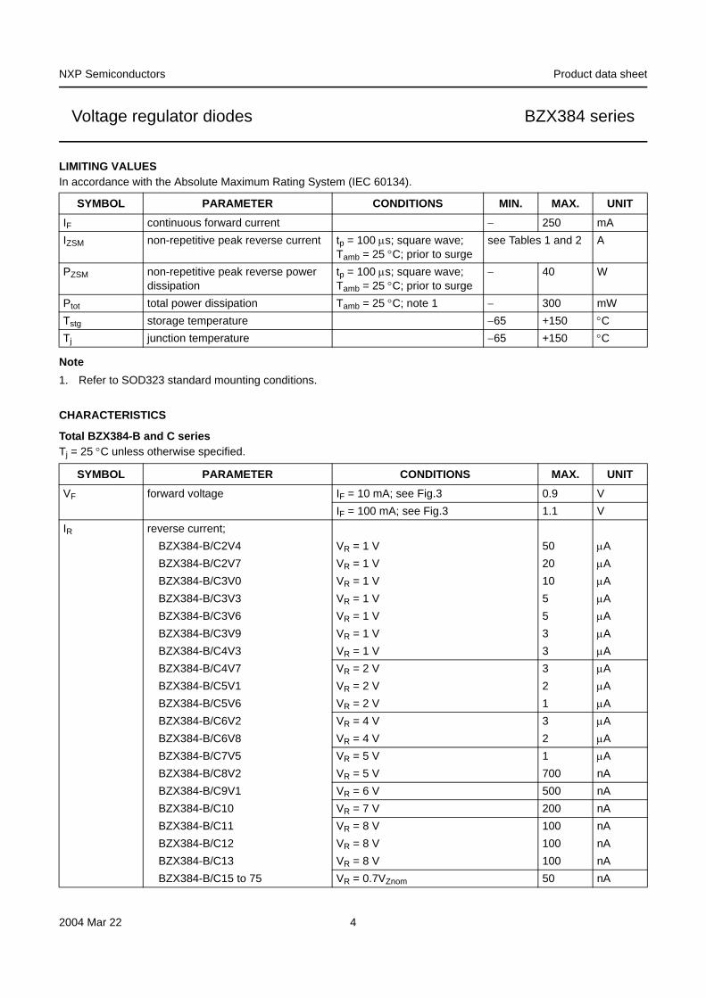
LIMITING VALUESIn accordance with the Absolute Maximum Rating System (IEC 60134).
Note1. Refer to SOD323 standard mounting conditions.
CHARACTERISTICS
Total BZX384-B and C seriesTj = 25 °C unless otherwise specified.
SYMBOL PARAMETER CONDITIONS MIN. MAX. UNITIF continuous forward current − 250 mAIZSM non-repetitive peak reverse current tp = 100 μs; square wave;
Tamb = 25 °C; prior to surgesee Tables 1 and 2 A
PZSM non-repetitive peak reverse power dissipation
tp = 100 μs; square wave; Tamb = 25 °C; prior to surge
− 40 W
Ptot total power dissipation Tamb = 25 °C; note 1 − 300 mWTstg storage temperature −65 +150 °CTj junction temperature −65 +150 °C
SYMBOL PARAMETER CONDITIONS MAX. UNITVF forward voltage IF = 10 mA; see Fig.3 0.9 V
IF = 100 mA; see Fig.3 1.1 VIR reverse current;
BZX384-B/C2V4 VR = 1 V 50 μABZX384-B/C2V7 VR = 1 V 20 μABZX384-B/C3V0 VR = 1 V 10 μABZX384-B/C3V3 VR = 1 V 5 μABZX384-B/C3V6 VR = 1 V 5 μABZX384-B/C3V9 VR = 1 V 3 μABZX384-B/C4V3 VR = 1 V 3 μABZX384-B/C4V7 VR = 2 V 3 μABZX384-B/C5V1 VR = 2 V 2 μABZX384-B/C5V6 VR = 2 V 1 μABZX384-B/C6V2 VR = 4 V 3 μABZX384-B/C6V8 VR = 4 V 2 μABZX384-B/C7V5 VR = 5 V 1 μABZX384-B/C8V2 VR = 5 V 700 nABZX384-B/C9V1 VR = 6 V 500 nABZX384-B/C10 VR = 7 V 200 nABZX384-B/C11 VR = 8 V 100 nABZX384-B/C12 VR = 8 V 100 nABZX384-B/C13 VR = 8 V 100 nABZX384-B/C15 to 75 VR = 0.7VZnom 50 nA
2004 Mar 22 4
2004 Mar 22
NX
P S
emiconductors
Product data sheet
Voltage regulator diodesB
ZX384 series
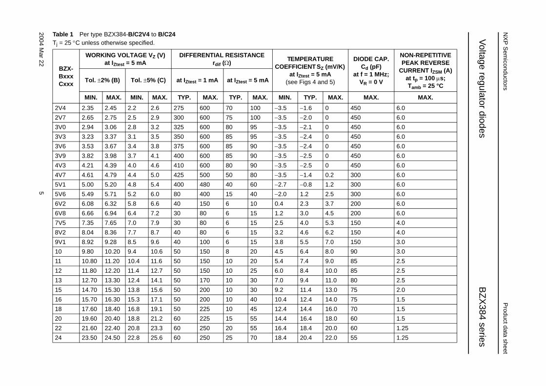
Table 1 Per type BZX384-B/C2V4 to B/C24Tj = 25 °C unless otherwise specified.
BZX-Bxxx
WORKING VOLTAGE VZ (V)at IZtest = 5 mA
DIFFERENTIAL RESISTANCE rdif (Ω) TEMPERATURE
COEFFICIENT SZ (mV/K) at IZtest = 5 mA
DIODE CAP. Cd (pF)
at f = 1 MHz;R = 0 V
NON-REPETITIVE PEAK REVERSE
CURRENT IZSM (A) at tp = 100 μs; Tamb = 25 °C
Tol. ±2% (B) Tol. ±5% (C) at I = 1 mA at I = 5 mA
MAX. MAX.6.06.06.06.06.06.06.06.06.06.06.06.04.04.03.03.02.52.52.52.01.51.51.51.251.25
5
Cxxx (see Figs 4 and 5) VZtest Ztest
MIN. MAX. MIN. MAX. TYP. MAX. TYP. MAX. MIN. TYP. MAX.2V4 2.35 2.45 2.2 2.6 275 600 70 100 −3.5 −1.6 0 4502V7 2.65 2.75 2.5 2.9 300 600 75 100 −3.5 −2.0 0 4503V0 2.94 3.06 2.8 3.2 325 600 80 95 −3.5 −2.1 0 4503V3 3.23 3.37 3.1 3.5 350 600 85 95 −3.5 −2.4 0 4503V6 3.53 3.67 3.4 3.8 375 600 85 90 −3.5 −2.4 0 4503V9 3.82 3.98 3.7 4.1 400 600 85 90 −3.5 −2.5 0 4504V3 4.21 4.39 4.0 4.6 410 600 80 90 −3.5 −2.5 0 4504V7 4.61 4.79 4.4 5.0 425 500 50 80 −3.5 −1.4 0.2 3005V1 5.00 5.20 4.8 5.4 400 480 40 60 −2.7 −0.8 1.2 3005V6 5.49 5.71 5.2 6.0 80 400 15 40 −2.0 1.2 2.5 3006V2 6.08 6.32 5.8 6.6 40 150 6 10 0.4 2.3 3.7 2006V8 6.66 6.94 6.4 7.2 30 80 6 15 1.2 3.0 4.5 2007V5 7.35 7.65 7.0 7.9 30 80 6 15 2.5 4.0 5.3 1508V2 8.04 8.36 7.7 8.7 40 80 6 15 3.2 4.6 6.2 1509V1 8.92 9.28 8.5 9.6 40 100 6 15 3.8 5.5 7.0 15010 9.80 10.20 9.4 10.6 50 150 8 20 4.5 6.4 8.0 9011 10.80 11.20 10.4 11.6 50 150 10 20 5.4 7.4 9.0 8512 11.80 12.20 11.4 12.7 50 150 10 25 6.0 8.4 10.0 8513 12.70 13.30 12.4 14.1 50 170 10 30 7.0 9.4 11.0 8015 14.70 15.30 13.8 15.6 50 200 10 30 9.2 11.4 13.0 7516 15.70 16.30 15.3 17.1 50 200 10 40 10.4 12.4 14.0 7518 17.60 18.40 16.8 19.1 50 225 10 45 12.4 14.4 16.0 7020 19.60 20.40 18.8 21.2 60 225 15 55 14.4 16.4 18.0 6022 21.60 22.40 20.8 23.3 60 250 20 55 16.4 18.4 20.0 6024 23.50 24.50 22.8 25.6 60 250 25 70 18.4 20.4 22.0 55
2004 Mar 22
NX
P S
emiconductors
Product data sheet
Voltage regulator diodesB
ZX384 series
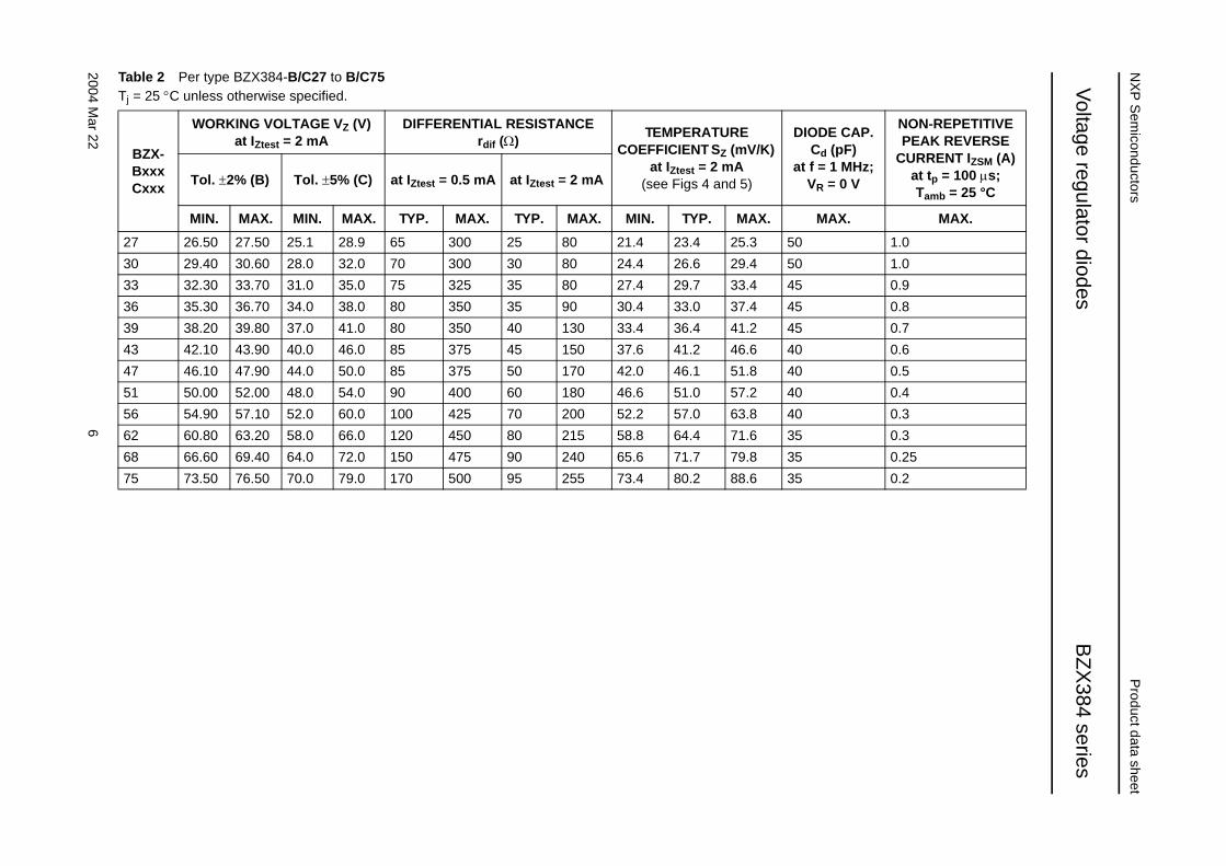
Table 2 Per type BZX384-B/C27 to B/C75Tj = 25 °C unless otherwise specified.
BZX-Bxxx
WORKING VOLTAGE VZ (V)at IZtest = 2 mA
DIFFERENTIAL RESISTANCE rdif (Ω) TEMPERATURE
COEFFICIENT SZ (mV/K) at IZtest = 2 mA
DIODE CAP. Cd (pF)
at f = 1 MHz; R = 0 V
NON-REPETITIVE PEAK REVERSE
CURRENT IZSM (A) at tp = 100 μs; Tamb = 25 °C
Tol. ±2% (B) Tol. ±5% (C) at I = 0.5 mA at I = 2 mA
MAX. MAX.1.01.00.90.80.70.60.50.40.30.30.250.2
6
Cxxx (see Figs 4 and 5) VZtest Ztest
MIN. MAX. MIN. MAX. TYP. MAX. TYP. MAX. MIN. TYP. MAX.27 26.50 27.50 25.1 28.9 65 300 25 80 21.4 23.4 25.3 5030 29.40 30.60 28.0 32.0 70 300 30 80 24.4 26.6 29.4 5033 32.30 33.70 31.0 35.0 75 325 35 80 27.4 29.7 33.4 4536 35.30 36.70 34.0 38.0 80 350 35 90 30.4 33.0 37.4 4539 38.20 39.80 37.0 41.0 80 350 40 130 33.4 36.4 41.2 4543 42.10 43.90 40.0 46.0 85 375 45 150 37.6 41.2 46.6 4047 46.10 47.90 44.0 50.0 85 375 50 170 42.0 46.1 51.8 4051 50.00 52.00 48.0 54.0 90 400 60 180 46.6 51.0 57.2 4056 54.90 57.10 52.0 60.0 100 425 70 200 52.2 57.0 63.8 4062 60.80 63.20 58.0 66.0 120 450 80 215 58.8 64.4 71.6 3568 66.60 69.40 64.0 72.0 150 475 90 240 65.6 71.7 79.8 3575 73.50 76.50 70.0 79.0 170 500 95 255 73.4 80.2 88.6 35
NXP Semiconductors Product data sheet
Voltage regulator diodes BZX384 series
THERMAL CHARACTERISTICS
Notes1. Device mounted on an FR4 printed-circuit board.2. Soldering point of the cathode tab.
SYMBOL PARAMETER CONDITIONS VALUE UNITRth(j-a) thermal resistance from junction
to ambientnote 1 415 K/W
Rth(j-s) thermal resistance from junction to soldering point
note 2 110 K/W
2004 Mar 22 7
NXP Semiconductors Product data sheet
Voltage regulator diodes BZX384 series
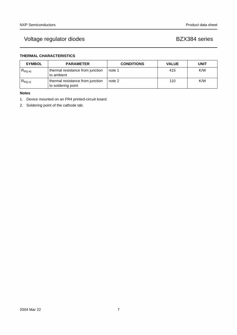
GRAPHICAL DATA
Fig.2 Maximum permissible non-repetitive peak reverse power dissipation versus duration.
handbook, halfpage
MBG801103
1 duration (ms)
PZSM(W)
10
102
10−1
10
1
(1)
(2)
(1) Tj = 25 °C (prior to surge).(2) Tj = 150 °C (prior to surge).
Fig.3 Forward current as a function of forward voltage; typical values.
handbook, halfpage
0.6 1
300
100
0
200
MBG781
0.8 VF (V)
IF(mA)
Tj = 25 °C.
Fig.4 Temperature coefficient as a function of working current; typical values.
handbook, halfpage
0 60
0
−2
−3
−1
MBG783
20 40 IZ (mA)
SZ(mV/K) 4V3
3V9
3V6
3V0
2V42V7
3V3
BZX384-B/C2V4 to B/C4V3.Tj = 25 to 150 °C.
Fig.5 Temperature coefficient as a function of working current; typical values.
handbook, halfpage
0 2016
10
0
−5
5
MBG782
4 8 12IZ (mA)
SZ(mV/K)
4V7
12
11
10
9V1
8V27V56V8
6V2
5V6
5V1
BZX384-B/C4V7 to B/C12.Tj = 25 to 150 °C.
2004 Mar 22 8
NXP Semiconductors Product data sheet
Voltage regulator diodes BZX384 series
PACKAGE OUTLINE
REFERENCESOUTLINEVERSION
EUROPEANPROJECTION
ISSUE DATEIEC JEDEC JEITA
SOD323 SC-76
SOD323
03-12-1706-03-16
Note1. The marking bar indicates the cathode
UNIT A
mm 0.051.10.8
0.400.25
0.250.10
1.81.6
1.351.15
2.72.3
0.450.15
A1max
DIMENSIONS (mm are the original dimensions)
Plastic surface-mounted package; 2 leads
0 1
(1)
21
2 mm
scale
bp c D E HD Q
0.250.15
Lp v
0.2
AD
A
E
Lp
bp
detail X
A1
c
Q
HD v AM
X
2004 Mar 22 9
NXP Semiconductors Product data sheet
Voltage regulator diodes BZX384 series
DATA SHEET STATUS
Notes1. Please consult the most recently issued document before initiating or completing a design.2. The product status of device(s) described in this document may have changed since this document was published
and may differ in case of multiple devices. The latest product status information is available on the Internet at URL http://www.nxp.com.
DOCUMENTSTATUS(1)
PRODUCT STATUS(2) DEFINITION
Objective data sheet Development This document contains data from the objective specification for product development.
Preliminary data sheet Qualification This document contains data from the preliminary specification. Product data sheet Production This document contains the product specification.
DISCLAIMERS
General ⎯ Information in this document is believed to be accurate and reliable. However, NXP Semiconductors does not give any representations or warranties, expressed or implied, as to the accuracy or completeness of such information and shall have no liability for the consequences of use of such information.
Right to make changes ⎯ NXP Semiconductors reserves the right to make changes to information published in this document, including without limitation specifications and product descriptions, at any time and without notice. This document supersedes and replaces all information supplied prior to the publication hereof.
Suitability for use ⎯ NXP Semiconductors products are not designed, authorized or warranted to be suitable for use in medical, military, aircraft, space or life support equipment, nor in applications where failure or malfunction of an NXP Semiconductors product can reasonably be expected to result in personal injury, death or severe property or environmental damage. NXP Semiconductors accepts no liability for inclusion and/or use of NXP Semiconductors products in such equipment or applications and therefore such inclusion and/or use is at the customer’s own risk.
Applications ⎯ Applications that are described herein for any of these products are for illustrative purposes only. NXP Semiconductors makes no representation or warranty that such applications will be suitable for the specified use without further testing or modification.
Limiting values ⎯ Stress above one or more limiting values (as defined in the Absolute Maximum Ratings System of IEC 60134) may cause permanent damage to the device. Limiting values are stress ratings only and operation of the device at these or any other conditions
above those given in the Characteristics sections of this document is not implied. Exposure to limiting values for extended periods may affect device reliability.
Terms and conditions of sale ⎯ NXP Semiconductors products are sold subject to the general terms and conditions of commercial sale, as published at http://www.nxp.com/profile/terms, including those pertaining to warranty, intellectual property rights infringement and limitation of liability, unless explicitly otherwise agreed to in writing by NXP Semiconductors. In case of any inconsistency or conflict between information in this document and such terms and conditions, the latter will prevail.
No offer to sell or license ⎯ Nothing in this document may be interpreted or construed as an offer to sell products that is open for acceptance or the grant, conveyance or implication of any license under any copyrights, patents or other industrial or intellectual property rights.
Export control ⎯ This document as well as the item(s) described herein may be subject to export control regulations. Export might require a prior authorization from national authorities.
Quick reference data ⎯ The Quick reference data is an extract of the product data given in the Limiting values and Characteristics sections of this document, and as such is not complete, exhaustive or legally binding.
2004 Mar 22 10
NXP Semiconductors
Contact information
For additional information please visit: http://www.nxp.com For sales offices addresses send e-mail to: [email protected]
© NXP B.V. 2009
All rights are reserved. Reproduction in whole or in part is prohibited without the prior written consent of the copyright owner.The information presented in this document does not form part of any quotation or contract, is believed to be accurate and reliable and may be changed without notice. No liability will be accepted by the publisher for any consequence of its use. Publication thereof does not convey nor imply any license
Customer notification
This data sheet was changed to reflect the new company name NXP Semiconductors, including new legal definitions and disclaimers. No changes were made to the technical content, except for package outline drawings which were updated to the latest version.
under patent- or other industrial or intellectual property rights.Printed in The Netherlands R76/02/pp11 Date of release: 2004 Mar 22 Document order number: 9397 750 12616