Bias-voltage-controlled magnetization switch in ferromagnetic semiconductor resonant tunneling...
20
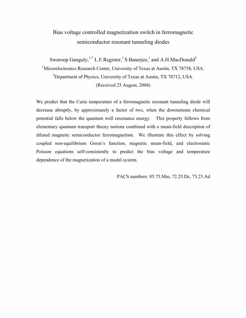
Bias voltage controlled magnetization switch in ferromagnetic semiconductor resonant tunneling diodes Swaroop Ganguly, 1,* L.F.Register, 1 S.Banerjee, 1 and A.H.MacDonald 2 1 Microelectronics Research Center, University of Texas at Austin, TX 78758, USA. 2 Department of Physics, University of Texas at Austin, TX 78712, USA. (Received 25 August, 2004) We predict that the Curie temperature of a ferromagnetic resonant tunneling diode will decrease abruptly, by approximately a factor of two, when the downstream chemical potential falls below the quantum well resonance energy. This property follows from elementary quantum transport theory notions combined with a mean-field description of diluted magnetic semiconductor ferromagnetism. We illustrate this effect by solving coupled non-equilibrium Green’s function, magnetic mean-field, and electrostatic Poisson equations self-consistently to predict the bias voltage and temperature dependence of the magnetization of a model system. PACS numbers: 85.75.Mm, 72.25.Dc, 73.23.Ad
Transcript of Bias-voltage-controlled magnetization switch in ferromagnetic semiconductor resonant tunneling...
Bias voltage controlled magnetization switch in ferromagnetic
semiconductor resonant tunneling diodes
Swaroop Ganguly,1,* L.F.Register,1 S.Banerjee,1 and A.H.MacDonald2
1Microelectronics Research Center, University of Texas at Austin, TX 78758, USA. 2Department of Physics, University of Texas at Austin, TX 78712, USA.
(Received 25 August, 2004)
We predict that the Curie temperature of a ferromagnetic resonant tunneling diode will
decrease abruptly, by approximately a factor of two, when the downstream chemical
potential falls below the quantum well resonance energy. This property follows from
elementary quantum transport theory notions combined with a mean-field description of
diluted magnetic semiconductor ferromagnetism. We illustrate this effect by solving
coupled non-equilibrium Green’s function, magnetic mean-field, and electrostatic
Poisson equations self-consistently to predict the bias voltage and temperature
dependence of the magnetization of a model system.
PACS numbers: 85.75.Mm, 72.25.Dc, 73.23.Ad
I. INTRODUCTION
Diluted magnetic semiconductors (DMS’s) that exhibit carrier-mediated
ferromagnetism1,2 have attracted interest because of new basic science questions that their
properties raise and because of their potential for applications. In this article we predict
that the magnetic properties of a resonant tunneling diode (RTD) with a DMS
ferromagnet3 quantum well, schematically illustrated in figure 1(a), will change abruptly
when the down stream chemical potential crosses the quantum well resonance energy.
The qualitative physics which leads to this effect is summarized by figure 1(b). In a
mean-field description, whose approximate validity in strongly metallic DMS
ferromagnets is now well established,4,5 the ferromagnetic transition temperature of the
quantum well system is determined by a competition between the entropic cost of
moment ordering and the exchange energy gained by aligning band spins opposite to
local moment spins. As we explain below, the Curie temperature is proportional to the
spin-susceptibility of the band electrons, and therefore proportional to the energy gained
by the paramagnetic band spin system when placed in an effective Zeeman field. In
figure 1(b), the Zeeman field is characterized by the splitting∆ between majority and
minority spin bands to which it gives rise. Standard transport theory assumptions imply
that state occupation numbers in the presence of a bias voltage are obtained by averaging
the Fermi factors of the up-stream and down-stream reservoirs of the RTD, with equal
weight if the upstream and downstream barriers are identical. As illustrated by the
arrows in figure 1(b), the gain in energy due to the Zeeman field can be thought of as
following from the replacement of minority spin states in the energy interval (0, 2∆ ) by
majority spin states in the interval ( 2−∆ ,0), with all energies measured from the
quantum well resonance (sub-band) energy. Since these states have occupation number 1
when the resonance energy is below the chemical potential of both reservoirs and 1/2
when the resonance energy is above the downstream chemical potential, the exchange
energy gain is halved at this crossing. In an ideal disorder-free system with a narrow
resonance, the Curie temperature will therefore drop by a factor of two.
This article is an examination of the idea explained above. In Section II we derive
an analytic expression for the Curie temperature implied by the argument of figure 1.
The simplifying assumptions used in this derivation are partially tested in Section III by
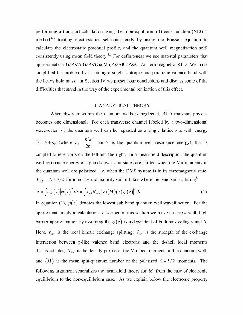
performing a transport calculation using the non-equilibrium Greens function (NEGF)
method,6,7 treating electrostatics self-consistently by using the Poisson equation to
calculate the electrostatic potential profile, and the quantum well magnetization self-
consistently using mean field theory.4,5 For definiteness we use material parameters that
approximate a GaAs/AlGaAs/(Ga,Mn)As/AlGaAs/GaAs ferromagnetic RTD. We have
simplified the problem by assuming a single isotropic and parabolic valence band with
the heavy hole mass. In Section IV we present our conclusions and discuss some of the
difficulties that stand in the way of the experimental realization of this effect.
II. ANALYTICAL THEORY
When disorder within the quantum wells is neglected, RTD transport physics
becomes one dimensional. For each transverse channel labeled by a two-dimensional
wavevector κ , the quantum well can be regarded as a single lattice site with energy
E κεΕ = + (where 2 2
*2mκκε = and E is the quantum well resonance energy), that is
coupled to reservoirs on the left and the right. In a mean-field description the quantum
well resonance energy of up and down spin states are shifted when the Mn moments in
the quantum well are polarized, i.e. when the DMS system is in its ferromagnetic state:
, 2E E↓ ↑ = ± ∆ for minority and majority spin orbitals where the band spin-splitting8
( ) ( ) ( ) ( ) ( )2 2pd pd Mnh z z dz J N z M z z dzϕ ϕ∆ ≈ =∫ ∫ . (1)
In equation (1), ( )zϕ denotes the lowest sub-band quantum well wavefunction. For the
approximate analytic calculations described in this section we make a narrow well, high
barrier approximation by assuming that ( )zϕ is independent of both bias voltages and ∆.
Here, pdh is the local kinetic exchange splitting, pdJ is the strength of the exchange
interaction between p-like valence band electrons and the d-shell local moments
discussed later, MnN is the density profile of the Mn local moments in the quantum well,
and M is the mean spin-quantum number of the polarized 5 / 2S = moments. The
following argument generalizes the mean-field theory for M from the case of electronic
equilibrium to the non-equilibrium case. As we explain below the electronic property
that enters the mean-field theory for the critical temperature is the band (Pauli) spin-
susceptibility. We now show that the spin-susceptibility is suddenly decreased when the
downstream chemical potential drops below the quantum well resonance energy.
The description of a non-equilibrium state in which two reservoirs with different
chemical potentials are coupled to a single atomic site, and current flows from the high
chemical potential reservoir to the low-chemical potential reservoir through that site, is
the simplest toy model of quantum transport theory. Our interest here is in determining
the influence of a bias voltage (i.e. a difference between the chemical potentials of the
reservoirs) on the magnetic state of a DMS quantum well. The key result from quantum
transport theory that we will need is the following simple expression7 for the steady-state
occupation of a quantum well state:
( ) ( )L RL R
L R L R
N f E f Eγ γγ γ γ γ
= ++ +
(2)
where, ( )( ) 1exp1
,, +−=
TkEf
BRLRL µ
are the Fermi functions for the left and right leads,
and Lγ , Rγ are the rates at which an electron inside the device will escape into the
left and right leads, respectively. We use this expression to find the electronic charge and
spin densities in the RTD quantum well. The couplings , ,L R L RTγ ∝ where 1, <<RLT are
the tunneling probability through the left and right barriers.9 For each spin subsystem, we
integrate over transverse kinetic energies and assume a single longitudinal resonance
level in the energy range of interest. We also assume degenerate statistics and parabolic
dispersion. Under these conditions, the 2D carrier density in the well is given by the
following expressions when 0M = :
( ) ( )2 L RL R
L R L R
N E Eγ γν µ µγ γ γ γ⎡ ⎤
= ⋅ ⋅ ⋅ − + ⋅ −⎢ ⎥+ +⎣ ⎦ for L R Eµ µ> > (3)
( )2 LL
L R
N Eγν µγ γ⎡ ⎤
= ⋅ ⋅ ⋅ −⎢ ⎥+⎣ ⎦ for L REµ µ> > (4)
where *
22mνπ
= is the 2D density of states and the factor of 2 accounts for spin
degeneracy.
For tall nearly symmetric barriers, that is 1 2L Rγ γ≈ ≈ , and a small applied bias
V , with respect to the band-edge in the emitter side, Lµ µ= , R Vµ µ= − by definition,
and / 2E Vε≈ − whereε is the resonance energy level at equilibrium, and all energies
are measured in electron volts. Now, for ( )/ 2 2R E V V Vµ µ ε µ ε> ⇒ − > − ⇒ < − , we
have from equation (3):
( ) ( )2 22
L R
L R
VN γ γν µ ε ν µ εγ γ
⎡ ⎤−= ⋅ ⋅ − + ⋅ ≈ ⋅ −⎢ ⎥+⎣ ⎦ (5)
Therefore, to lowest order inε , the 2D spin susceptibility has the same value as in the
equilibrium case:
( ) 0lim 1
N Nε ε
χχ νε ε ν↓ ↑
↑ ↓
− →↓ ↑
−≅ ≈ ⇒ ≈
− (6)
On the other hand, for ( )2RE Vµ µ ε> ⇒ > − , we get from equation (4):
( ) ( )2 2 2L
L R
N V Vγν µ ε ν µ εγ γ⎡ ⎤
= ⋅ ⋅ ⋅ − + ≈ − +⎢ ⎥+⎣ ⎦ (7)
which yields, for the 2D spin susceptibility:
12
L
L R
γχν γ γ≈ ≈
+ (8)
We note, from equations (5) and (7) that the total carrier concentration N is continuous
at the applied voltage ( )2SV V µ ε= ≅ − , even though the spin susceptibility exhibits a
sharp drop at this point as implied by equations (6) and (8). Finally,
when 0 / 2 0 2E V Vε ε< ⇒ − < ⇒ > , obviously 0 0N χ→ ⇒ → . Therefore when the
bias potential goes to 2CV ε≅ , we expect the total concentration to decrease sharply and
the spin susceptibility to vanish. Thus, the spin susceptibility is predicted to decrease with
increasing voltage to zero from its equilibrium value in two steps, at SV and CV . This
qualitative argument is supported by numerical model simulations illustrated in figure 2
and described below.
The mean-field critical temperature in equilibrium DMS systems can be found by
equating the Zeeman mean-field experienced by band electrons h due to their interaction
with induced local moment polarization, with the mean-field necessary to create a small
spin density ( ) 2s n n↑ ↓= − . Inserting the text book expression for local moment spin-
susceptibility, one obtains:5
( )2 13
pd Mn
B C
J S S N sh s
k T χ+
= = (9)
where χ denotes the susceptibility. Using equations (1) and (6) in (9) gives:
( ) ( )( ) ( ) ( ) ( ) ( )( )
( )2 2 2
2
2 2n z n z z dz N N z z dz N N
z dz
ϕ ϕ ψε ε
χ χχ ψ↑ ↓ ↑ ↓ ↑ ↓
↓ ↑
− − −− = = =∫ ∫
∫ (10)
where ,N↑ ↓ denote 2D carrier densities as usual, ( )zψ the non-equilibrium RTD wave
function, the integrals are over the width of the well and χ is the 2D spin susceptibility
computed in equations (6) and (8). For quantum wells in equilibrium ( ) ( )z zψ ϕ= ; using
equation (6) in (10), we trivially recover the familiar expression8 for the Curie
temperature in these systems: ( ) ( )
241
6pd Mn
CB C
J S S NT z dz
k Tν
ϕ+
= ∫ . For large-barrier
RTD’s, the approximation ( ) ( )z zψ ϕ= should still be valid in the non-equilibrium case.
We therefore predict that the critical temperature should fall from this equilibrium
quantum-well expression, to approximately half this value when the down-stream
chemical potential falls below the quantum-well resonance energy.
III. NUMERICAL SIMULATION
The simulated device consists of a highly p-doped GaAs emitter and collector,
Al0.8Ga0.2As barriers 10Å in thickness, and a 10Å thick (Ga,Mn)As well. We use the
following material parameters, from Davies:10 GaAs/AlGaAs band-offset – 0.38eV, hole
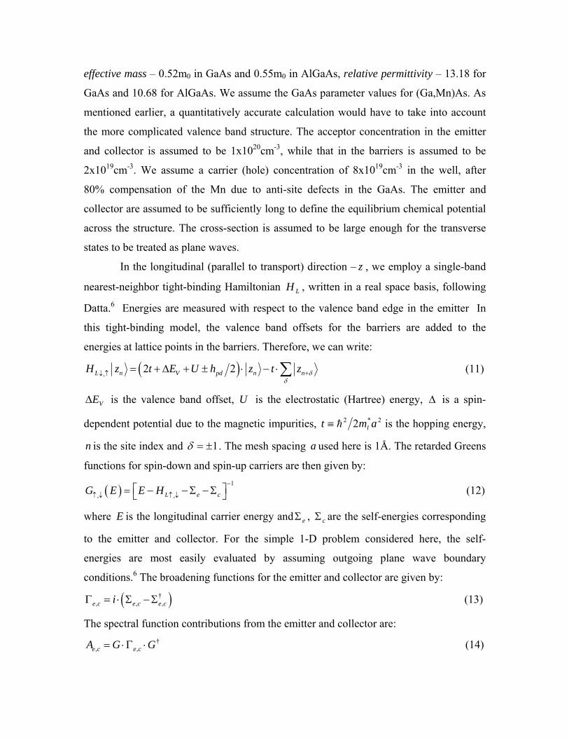
effective mass – 0.52m0 in GaAs and 0.55m0 in AlGaAs, relative permittivity – 13.18 for
GaAs and 10.68 for AlGaAs. We assume the GaAs parameter values for (Ga,Mn)As. As
mentioned earlier, a quantitatively accurate calculation would have to take into account
the more complicated valence band structure. The acceptor concentration in the emitter
and collector is assumed to be 1x1020cm-3, while that in the barriers is assumed to be
2x1019cm-3. We assume a carrier (hole) concentration of 8x1019cm-3 in the well, after
80% compensation of the Mn due to anti-site defects in the GaAs. The emitter and
collector are assumed to be sufficiently long to define the equilibrium chemical potential
across the structure. The cross-section is assumed to be large enough for the transverse
states to be treated as plane waves.
In the longitudinal (parallel to transport) direction – z , we employ a single-band
nearest-neighbor tight-binding Hamiltonian LH , written in a real space basis, following
Datta.6 Energies are measured with respect to the valence band edge in the emitter In
this tight-binding model, the valence band offsets for the barriers are added to the
energies at lattice points in the barriers. Therefore, we can write:
( ), 2 2L n V pd n nH z t E U h z t z δδ
+↓ ↑ = + ∆ + ± ⋅ − ⋅∑ (11)
VE∆ is the valence band offset, U is the electrostatic (Hartree) energy, ∆ is a spin-
dependent potential due to the magnetic impurities, 2*2 2 amt l≡ is the hopping energy,
n is the site index and 1±=δ . The mesh spacing a used here is 1Å. The retarded Greens
functions for spin-down and spin-up carriers are then given by:
( )1
, ,L e cG E E H−
↑ ↓ ↑ ↓⎡ ⎤= − −Σ −Σ⎣ ⎦ (12)
where E is the longitudinal carrier energy and eΣ , cΣ are the self-energies corresponding
to the emitter and collector. For the simple 1-D problem considered here, the self-
energies are most easily evaluated by assuming outgoing plane wave boundary
conditions.6 The broadening functions for the emitter and collector are given by:
( )†, , ,e c e c e ciΓ = ⋅ Σ −Σ (13)
The spectral function contributions from the emitter and collector are: †
, ,e c e cA G G= ⋅Γ ⋅ (14)
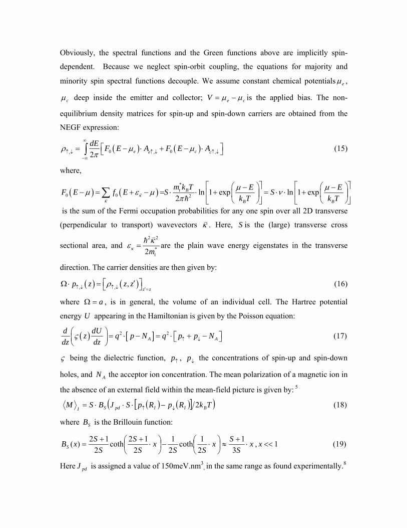
Obviously, the spectral functions and the Green functions above are implicitly spin-
dependent. Because we neglect spin-orbit coupling, the equations for majority and
minority spin spectral functions decouple. We assume constant chemical potentials eµ ,
cµ deep inside the emitter and collector; ceV µµ −= is the applied bias. The non-
equilibrium density matrices for spin-up and spin-down carriers are obtained from the
NEGF expression:
( ) ( )0 0, , ,2 e ce c
dE F E A F E Aρ µ µπ
∞
↑ ↓ ↑ ↓ ↑ ↓−∞
⎡ ⎤= − ⋅ + − ⋅⎣ ⎦∫ (15)
where,
( ) ( )*
0 0 2 ln 1 exp ln 1 exp2
t B
B B
m k T E EF E f E S Sk T k Tκ
κ
µ µµ ε µ νπ
⎡ ⎤ ⎡ ⎤⎛ ⎞ ⎛ ⎞− −− = + − = ⋅ ⋅ + = ⋅ ⋅ +⎢ ⎥ ⎢ ⎥⎜ ⎟ ⎜ ⎟
⎝ ⎠ ⎝ ⎠⎣ ⎦ ⎣ ⎦∑
is the sum of the Fermi occupation probabilities for any one spin over all 2D transverse
(perpendicular to transport) wavevectors κ . Here, S is the (large) transverse cross
sectional area, and 2 2
*2 tmκκε = are the plain wave energy eigenstates in the transverse
direction. The carrier densities are then given by:
( ) ( ), , ,z z
p z z zρ↑ ↓ ↑ ↓ ′=⎡ ⎤′Ω ⋅ = ⎣ ⎦ (16)
where a=Ω , is in general, the volume of an individual cell. The Hartree potential
energy U appearing in the Hamiltonian is given by the Poisson equation:
( ) [ ]2 2A A
d dUz q p N q p p Ndz dz
ς ↑ ↓⎛ ⎞ = ⋅ − = ⋅ ⎡ + − ⎤⎜ ⎟ ⎣ ⎦⎝ ⎠
(17)
ς being the dielectric function, ↑p , ↓p the concentrations of spin-up and spin-down
holes, and AN the acceptor ion concentration. The mean polarization of a magnetic ion in
the absence of an external field within the mean-field picture is given by: 5
( ) ( )[ ]( )TkRpRpSJBSM BIIpdSI2↓↑ −⋅⋅⋅= (18)
where SB is the Brillouin function:
⎟⎠⎞
⎜⎝⎛ ⋅−⎟
⎠⎞
⎜⎝⎛ ⋅
++= x
SSx
SS
SSxBS 2
1coth21
212coth
212)( x
SS
⋅+
≈3
1 , 1<<x (19)
Here pdJ is assigned a value of 150meV.nm3, in the same range as found experimentally.8
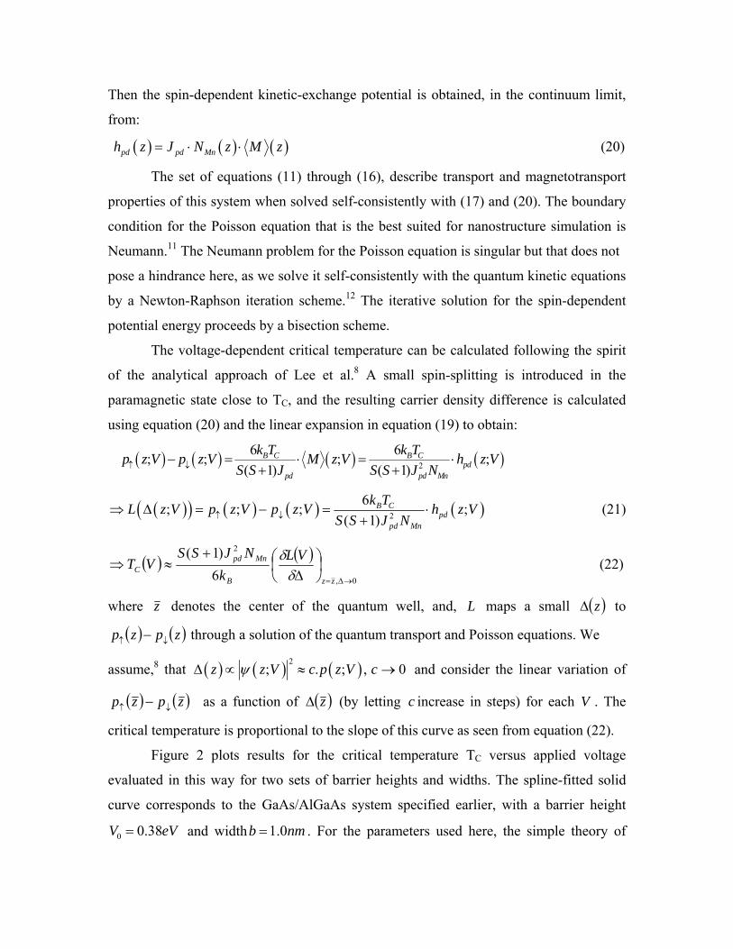
Then the spin-dependent kinetic-exchange potential is obtained, in the continuum limit,
from:
( ) ( ) ( )pd pd Mnh z J N z M z= ⋅ ⋅ (20)
The set of equations (11) through (16), describe transport and magnetotransport
properties of this system when solved self-consistently with (17) and (20). The boundary
condition for the Poisson equation that is the best suited for nanostructure simulation is
Neumann.11 The Neumann problem for the Poisson equation is singular but that does not
pose a hindrance here, as we solve it self-consistently with the quantum kinetic equations
by a Newton-Raphson iteration scheme.12 The iterative solution for the spin-dependent
potential energy proceeds by a bisection scheme.
The voltage-dependent critical temperature can be calculated following the spirit
of the analytical approach of Lee et al.8 A small spin-splitting is introduced in the
paramagnetic state close to TC, and the resulting carrier density difference is calculated
using equation (20) and the linear expansion in equation (19) to obtain:
( ) ( ) ( ) ( )2
6 6; ; ; ;( 1) ( 1)
B C B Cpd
pd pd Mn
k T k Tp z V p z V M z V h z VS S J S S J N↑ ↓− = ⋅ = ⋅
+ +
( )( ) ( ) ( ) ( )2
6; ; ; ;( 1)
B Cpd
pd Mn
k TL z V p z V p z V h z VS S J N↑ ↓⇒ ∆ = − = ⋅
+ (21)
( ) ( )0,
2
6)1(
→∆=
⎟⎠⎞
⎜⎝⎛
∆
+≈⇒
zzB
MnpdC
VLk
NJSSVT
δδ (22)
where z denotes the center of the quantum well, and, L maps a small ( )z∆ to
( ) ( )zpzp ↓↑ − through a solution of the quantum transport and Poisson equations. We
assume,8 that ( ) ( ) ( )2; . ; ,z z V c p z Vψ∆ ∝ ≈ 0→c and consider the linear variation of
( ) ( )zpzp ↓↑ − as a function of ( )z∆ (by letting c increase in steps) for each V . The
critical temperature is proportional to the slope of this curve as seen from equation (22).
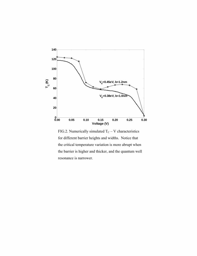
Figure 2 plots results for the critical temperature TC versus applied voltage
evaluated in this way for two sets of barrier heights and widths. The spline-fitted solid
curve corresponds to the GaAs/AlGaAs system specified earlier, with a barrier height
0 0.38V eV= and width 1.0b nm= . For the parameters used here, the simple theory of
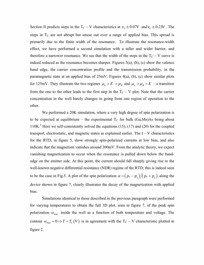
Section II predicts steps in the TC – V characteristics at 0.07Sv V≅ and 0.23Cv V≅ . The
steps in TC are not abrupt but smear out over a range of applied bias. This spread is
primarily due to the finite width of the resonance. To illustrate the resonance-width
effect, we have performed a second simulation with a taller and wider barrier, and
therefore a narrower resonance. We see that the width of the steps in the TC – V curve is
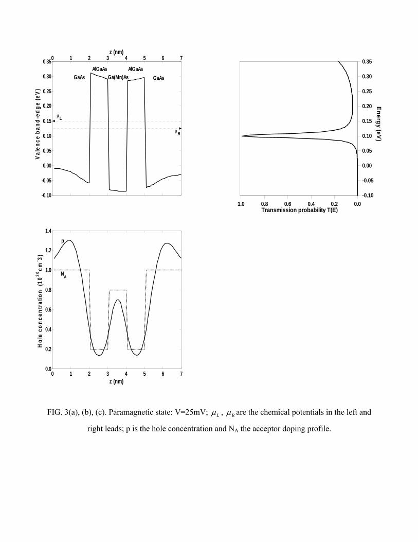
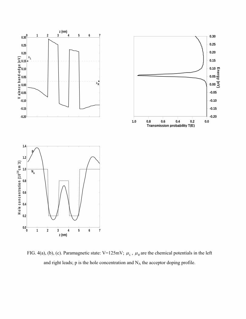
indeed reduced as the resonance becomes sharper. Figures 3(a), (b), (c) show the valence
band edge, the carrier concentration profile and the transmission probability, in the
paramagnetic state at an applied bias of 25mV; Figures 4(a), (b), (c) show similar plots
for 125mV. They illustrate the two regimes L REµ µ> > and L R Eµ µ> > – a transition
from the one to the other leads to the first step in the TC – V plot. Note that the carrier
concentration in the well barely changes in going from one region of operation to the
other.
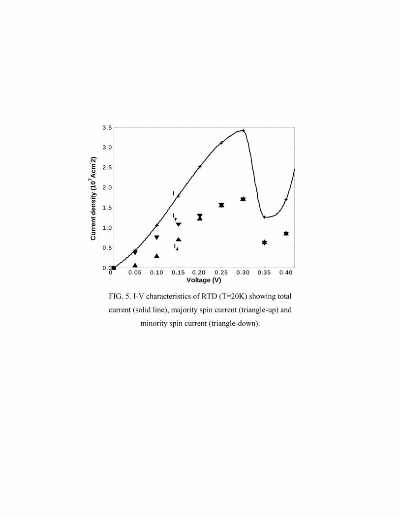
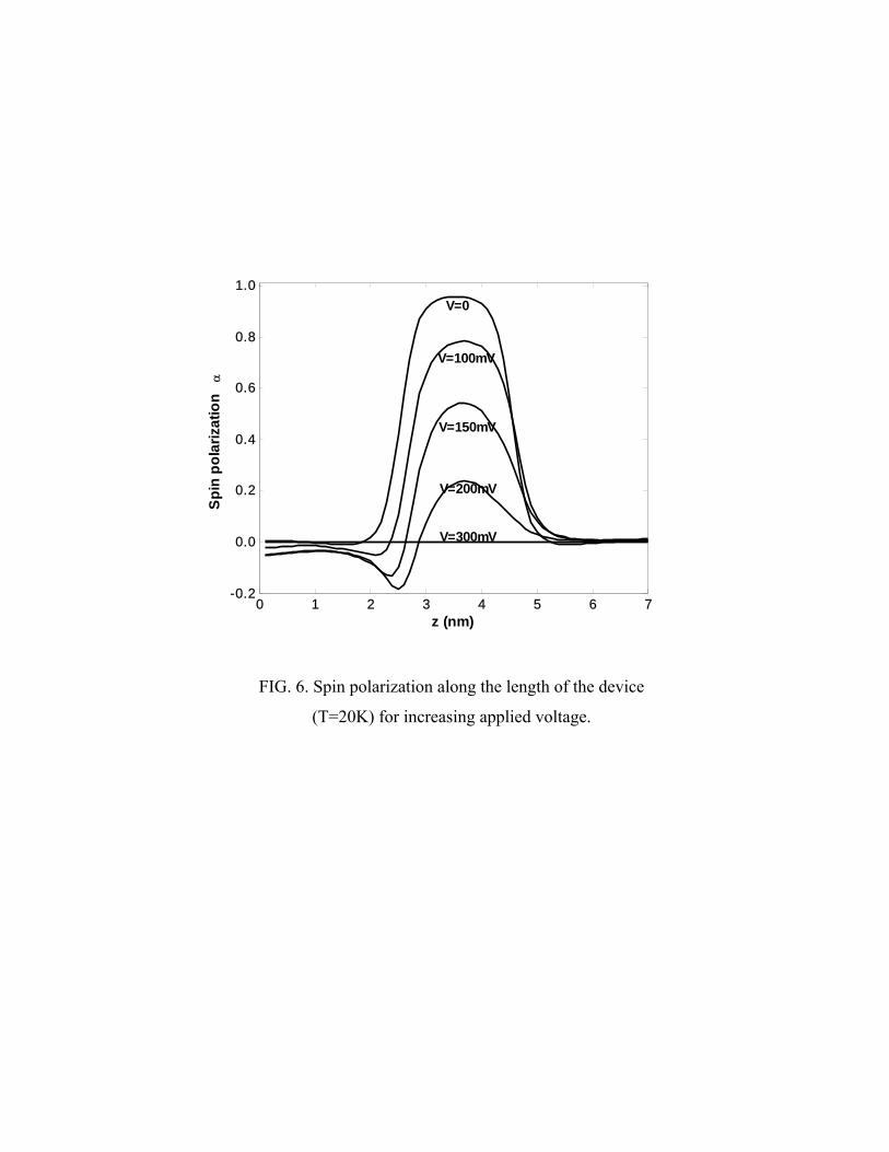
We performed a 20K simulation, where a very high degree of spin polarization is
to be expected at equilibrium – the experimental TC for bulk (Ga,Mn)As being about
110K.2 Here we self-consistently solved the equations (15), (17) and (20) for the coupled
transport, electrostatic, and magnetic states as explained earlier. The I – V characteristics
for the RTD, in figure 5, show strongly spin-polarized currents at low bias, and also
indicate that the magnetism vanishes around 300mV. From the analytic theory, we expect
vanishing magnetization to occur when the resonance is pulled down below the band-
edge on the emitter side. At this point, the current should fall sharply giving rise to the
well-known negative differential resistance (NDR) regime of the RTD; this is indeed seen
to be the case in Fig.5. A plot of the spin polarization ( ) ( )p p p pα ↑ ↓ ↑ ↓= − + along the
device shown in figure 7, clearly illustrates the decay of the magnetization with applied
bias.
Simulations identical to those described in the previous paragraph were performed
for varying temperatures to obtain the full 3D plot, seen in figure 7, of the peak spin
polarization maxα inside the well as a function of both temperature and voltage. The
contour ( )max 0 CT T Vα = ⇒ = is in agreement with the TC – V characteristic plotted in
figure 2.
IV. CONCLUSIONS
In this paper we have considered the coupling between magnetic and transport
properties of a resonant tunneling diode (RTD) with a diluted-magnetic-semiconductor
quantum well. The large literature on RTD structures has generally focused on the region
of negative differential conductance which occurs when the quantum well resonance
energy falls below the emitter band-edge. In this paper we predict that the ferromagnetic
transition temperature of the quantum well system decreases abruptly by approximately a
factor of two when the Fermi level of the collector falls below the quantum well
resonance energy, a condition that in typical quantum well structures holds over a broad
interval of bias voltages below the negative differential conductance regime. The
ferromagnetic transition temperature of the quantum well is expected to drop to near zero
in the negative differential conductance regime.
The voltage dependence of the critical temperature and of the spin-polarization at
a given temperature that is predicted here could be verified by simply measuring the RTD
I-V characteristics or more directly by magnetic or optical circular dichroism13
measurements. The prediction of a bias voltage dependent magnetic phase transition
temperature is potentially interesting for applications. For example the three step TC – V
characteristic might possibly suggest potential as a three-level logic device. More
practically perhaps, this novel effect could also, when operated at an appropriate
temperature, allow a small bias voltage to change the quantum well system between
magnetic and non-magnetic states.
There are a number of practical difficulties that would have to be overcome for
this idea to be tested experimentally, as well as a number of theoretical issues that require
further attention. On the materials and experiment side, the geometry we have
considered, in which the magnetic layer is the quantum well of a RTD, requires that
AlGaAs be grown on top of (Ga,Mn)As at low-temperatures, in order to avoid
precipitation of Mn and MnAs intermetallic compounds. Low temperature growth is
known to lead to low quality interfaces14 and will no doubt lead to inhomogeneous
broadening of the sharp quantum well resonance that is responsible for the relatively
abrupt decrease in the ferromagnetic transition temperature in our models. Verification
and refinement of the effect we propose would have to go hand in hand with advances in
epitaxial growth techniques in (Ga,Mn)As/AlGaAs systems in order to realize the abrupt
transition temperature changes that occur in our simple model. On the theoretical side,
our predictions would be altered somewhat by using a more realistic model for the
semiconductor valence bands. This kind of improvement in the theory is readily
implemented. More challenging is the analysis of the importance of corrections to the
mean-field theory that we employ. For a single parabolic band system, a two-dimensional
(Ga,Mn)As ferromagnet has vanishing spin-stiffness, implying that corrections to mean-
field theory have an overriding importance.15 For a valence band system, however, the
finite well width creates a large anisotropy gap and corrections to the mean-field theory
are likely to be less important.
ACKNOWLEDGEMENTS
This work was supported in part by the MARCO MSD Focus Center NSF, and
the Texas Advanced Technology Program. AHM was supported by the Welch
Foundation, by the Department of Energy under grant DE-FG03-02ER45958, and by the
DARPA SpinS program. Swaroop Ganguly would like to thank Prof. Supriyo Datta for
helpful discussions.
REFERENCE * Electronic Address: [email protected] 1 T. Story, R.R. Galazka, R.B. Frankel and P.A. Wolff, Phys. Rev. Lett. 56, 777
(1986). 2 H. Ohno, H. Munekata, T. Penney, S. von Molnar, and L.L. Chang, Phys. Rev. Lett.
68, 2664 (1992). 3 All II-VI RTD’s with paramagnetic DMS quantum wells have been demonstrated
by C. Gould, A. Slobodskyy, T. Slobodskyy, P. Grabs, C. R. Becker, G. Schmidt, L.
W. Molenkamp, Physica Status Solidi B 241 (3), 708 (2004). DMS ferromagnetism
is most robust in (III,Mn)V materials grown by low temperature MBE. The growth
of RTD’s with (III,Mn)V quantum wells presents challenges that have not yet been
met. 4 T. Dietl and H. Ohno, MRS Bulletin 28 (10), 714 (2003). 5 J. König, J. Schliemann, T. Jungwirth and A.H. MacDonald: in Electronic Structure
and Magnetism of Complex Materials, ed. by D.J. Singh and D.A.
Papaconstantopoulos (Springer Verlag 2002). 6 S. Datta, Superlattices and Microstructures 28 (4), 253 (2000). 7 S. Datta, IEDM Tech. Digest, 703 (2002). 8 B. Lee, T. Jungwirth, and A. MacDonald, Phys. Rev. B 61, 15606-15609 (2000). 9 S. Datta, Electronic Transport in Mesoscopic Systems (Cambridge University Press,
1995); Chapter 6. 10 J.H. Davies, The Physics of Low-dimensional Semiconductors (Cambridge
University Press, 1998); Appendix 3. 11 Z. Ren, R. Venugopal, S. Datta, M. Lundstrom, D. Jovanovic, and J.G. Fossum,
Proceedings of IEDM, 2000. 12 R. Lake, G. Klimeck, R. C. Bowen, and D. Jovanovic, J. Appl. Phys. 81 (12), 7845
(1997). 13 R. Fiederling , P. Grabs, W. Ossau, G. Schmidt, and L.W.Molenkamp, Applied
Physics Letters 82 (13), 2160 (2003). 14 H. Ohno, F. Matsukura, and Y. Ohno, Solid State Communications 119, 281 (2001). 15 J. König and Allan H. MacDonald, Phys. Rev. Lett. 91, 077202 (2003).
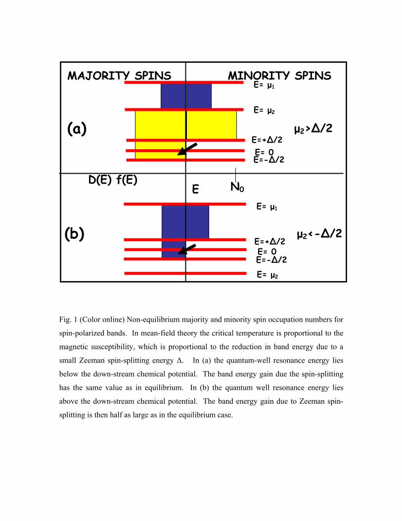
Fig. 1 (Color online) Non-equilibrium majority and minority spin occupation numbers for
spin-polarized bands. In mean-field theory the critical temperature is proportional to the
magnetic susceptibility, which is proportional to the reduction in band energy due to a
small Zeeman spin-splitting energy ∆. In (a) the quantum-well resonance energy lies
below the down-stream chemical potential. The band energy gain due the spin-splitting
has the same value as in equilibrium. In (b) the quantum well resonance energy lies
above the down-stream chemical potential. The band energy gain due to Zeeman spin-
splitting is then half as large as in the equilibrium case.
E
E=-∆/2 E= 0 E=+∆/2
E= µ2
E= µ1
D(E) f(E) N0
MAJORITY SPINS MINORITY SPINS
E=-∆/2 E= 0E=+∆/2
E= µ2
E= µ1
(a)
(b)
µ2>∆/2
µ2<-∆/2
0.00 0.05 0.10 0.15 0.20 0.25 0.300
20
40
60
80
100
120
140
Voltage (V)
T C (K)
V0=0.38eV, b=1.0nm
V0=0.45eV, b=1.2nm
FIG.2. Numerically simulated TC – V characteristics
for different barrier heights and widths. Notice that
the critical temperature variation is more abrupt when
the barrier is higher and thicker, and the quantum well
resonance is narrower.
z (nm)
Vale
nce
band
-edg
e (e
V)
0 1 2 3 4 5 6 7
-0.10
-0.05
0.00
0.05
0.10
0.15
0.20
0.25
0.30
0.35
µL
µR
GaAs AlGaAs
GaAs AlGaAs
Ga(Mn)As
-0.10
-0.05
0.00
0.05
0.10
0.15
0.20
0.25
0.30
0.35
0.00.20.40.60.81.0
Energy (eV)
Transmission probability T(E)
0 1 2 3 4 5 6 7
0.0
0.2
0.4
0.6
0.8
1.0
1.2
1.4
z (nm)
Hol
e co
ncen
tratio
n (1
020cm
- 3)
NA
p
FIG. 3(a), (b), (c). Paramagnetic state: V=25mV; Lµ , Rµ are the chemical potentials in the left and
right leads; p is the hole concentration and NA the acceptor doping profile.
0 1 2 3 4 5 6 7
-0.20
-0.15
-0.10
-0.05
0.00
0.05
0.10
0.15
0.20
0.25
0.30z (nm)
V al
ence
ban
d-ed
ge (e
V) µL
µR
-0.20
-0.15
-0.10
-0.05
0.00
0.05
0.10
0.15
0.20
0.25
0.30
0.00.20.40.60.81.0
Energy (eV)
Transmission probability T(E)
0 1 2 3 4 5 6 70.0
0.2
0.4
0.6
0.8
1.0
1.2
1.4
z (nm)
Hol
e co
ncen
tratio
n (1
020cm
- 3)
NA
p
FIG. 4(a), (b), (c). Paramagnetic state: V=125mV; Lµ , Rµ are the chemical potentials in the left
and right leads; p is the hole concentration and NA the acceptor doping profile.
0 0.05 0.10 0.15 0.20 0.25 0.30 0.35 0.400.0
0.5
1.0
1.5
2.0
2.5
3.0
3.5
Voltage (V)
Cur
rent
den
sity
(107 A
cm- 2)
I
I
I
FIG. 5. I-V characteristics of RTD (T=20K) showing total
current (solid line), majority spin current (triangle-up) and
minority spin current (triangle-down).
0 1 2 3 4 5 6 7-0.2
0.0
0.2
0.4
0.6
0.8
1.0
z (nm)
Spin
pol
ariz
atio
n α
V=0
V=100mV
V=200mV
V=300mV
V=150mV
FIG. 6. Spin polarization along the length of the device
(T=20K) for increasing applied voltage.
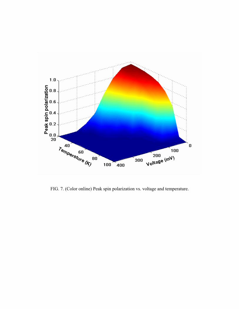
FIG. 7. (Color online) Peak spin polarization vs. voltage and temperature.