PI3A27518 - Diodes Incorporated
11
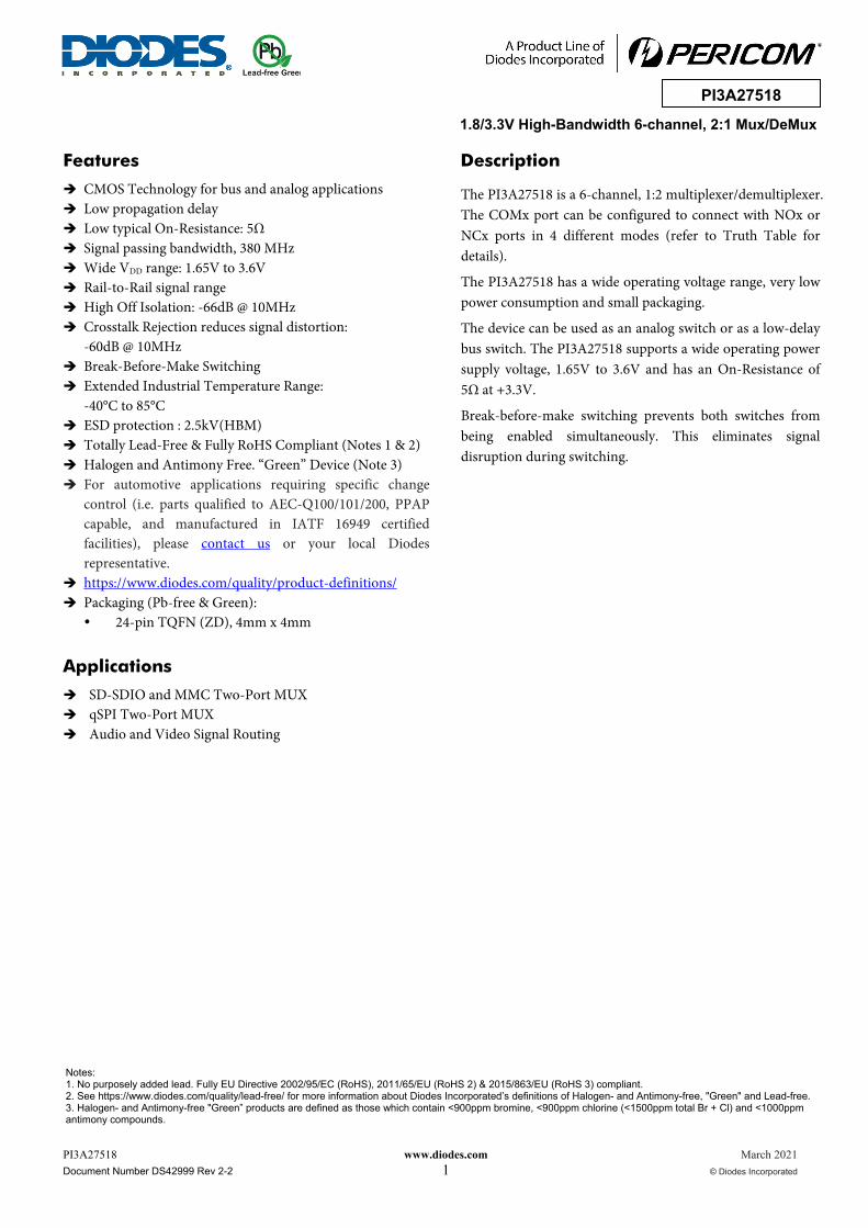
1.8/3.3V High-Bandwidth 6-channel, 2:1 Mux/DeMux PI3A27518 www.diodes.com March 2021 Document Number DS42999 Rev 2-2 1 © Diodes Incorporated PI3A27518 Features CMOS Technology for bus and analog applications Low propagation delay Low typical On-Resistance: 5Ω Signal passing bandwidth, 380 MHz Wide V DD range: 1.65V to 3.6V Rail-to-Rail signal range High Off Isolation: -66dB @ 10MHz Crosstalk Rejection reduces signal distortion: -60dB @ 10MHz Break-Before-Make Switching Extended Industrial Temperature Range: -40°C to 85°C ESD protection : 2.5kV(HBM) Totally Lead-Free & Fully RoHS Compliant (Notes 1 & 2) Halogen and Antimony Free. “Green” Device (Note 3) For automotive applications requiring specific change control (i.e. parts qualified to AEC-Q100/101/200, PPAP capable, and manufactured in IATF 16949 certified facilities), please contact us or your local Diodes representative. https://www.diodes.com/quality/product-definitions/ Packaging (Pb-free & Green): 24-pin TQFN (ZD), 4mm x 4mm Applications SD-SDIO and MMC Two-Port MUX qSPI Two-Port MUX Audio and Video Signal Routing Description The PI3A27518 is a 6-channel, 1:2 multiplexer/demultiplexer. The COMx port can be configured to connect with NOx or NCx ports in 4 different modes (refer to Truth Table for details). The PI3A27518 has a wide operating voltage range, very low power consumption and small packaging. The device can be used as an analog switch or as a low-delay bus switch. The PI3A27518 supports a wide operating power supply voltage, 1.65V to 3.6V and has an On-Resistance of 5Ω at +3.3V. Break-before-make switching prevents both switches from being enabled simultaneously. This eliminates signal disruption during switching. Notes: 1. No purposely added lead. Fully EU Directive 2002/95/EC (RoHS), 2011/65/EU (RoHS 2) & 2015/863/EU (RoHS 3) compliant. 2. See https://www.diodes.com/quality/lead-free/ for more information about Diodes Incorporated’s definitions of Halogen- and Antimony-free, "Green" and Lead-free. 3. Halogen- and Antimony-free "Green” products are defined as those which contain <900ppm bromine, <900ppm chlorine (<1500ppm total Br + Cl) and <1000ppm antimony compounds.
-
Upload
khangminh22 -
Category
Documents
-
view
0 -
download
0
Transcript of PI3A27518 - Diodes Incorporated
1.8/3.3V High-Bandwidth 6-channel, 2:1 Mux/DeMux
PI3A27518 www.diodes.com March 2021
Document Number DS42999 Rev 2-2 1 © Diodes Incorporated
PI3A27518
Features
CMOS Technology for bus and analog applications Low propagation delay Low typical On-Resistance: 5Ω Signal passing bandwidth, 380 MHz Wide VDD range: 1.65V to 3.6V Rail-to-Rail signal range High Off Isolation: -66dB @ 10MHz Crosstalk Rejection reduces signal distortion:
-60dB @ 10MHz Break-Before-Make Switching Extended Industrial Temperature Range:
-40°C to 85°C ESD protection : 2.5kV(HBM) Totally Lead-Free & Fully RoHS Compliant (Notes 1 & 2) Halogen and Antimony Free. “Green” Device (Note 3) For automotive applications requiring specific change
control (i.e. parts qualified to AEC-Q100/101/200, PPAP capable, and manufactured in IATF 16949 certified facilities), please contact us or your local Diodes representative.
https://www.diodes.com/quality/product-definitions/ Packaging (Pb-free & Green): 24-pin TQFN (ZD), 4mm x 4mm
Applications
SD-SDIO and MMC Two-Port MUX qSPI Two-Port MUX Audio and Video Signal Routing
Description
The PI3A27518 is a 6-channel, 1:2 multiplexer/demultiplexer. The COMx port can be configured to connect with NOx or NCx ports in 4 different modes (refer to Truth Table for details).
The PI3A27518 has a wide operating voltage range, very low power consumption and small packaging.
The device can be used as an analog switch or as a low-delay bus switch. The PI3A27518 supports a wide operating power supply voltage, 1.65V to 3.6V and has an On-Resistance of 5Ω at +3.3V.
Break-before-make switching prevents both switches from being enabled simultaneously. This eliminates signal disruption during switching.
Notes: 1. No purposely added lead. Fully EU Directive 2002/95/EC (RoHS), 2011/65/EU (RoHS 2) & 2015/863/EU (RoHS 3) compliant. 2. See https://www.diodes.com/quality/lead-free/ for more information about Diodes Incorporated’s definitions of Halogen- and Antimony-free, "Green" and Lead-free. 3. Halogen- and Antimony-free "Green” products are defined as those which contain <900ppm bromine, <900ppm chlorine (<1500ppm total Br + Cl) and <1000ppm antimony compounds.

PI3A27518 www.diodes.com March 2021
Document Number DS42999 Rev 2-2 2 © Diodes Incorporated
PI3A27518
Block Diagram
Function Table
Select Input Function
EN IN1 IN2
1 X X All Channels are OFF
0 0 0 NC1,2,3 Connected to COM1,2,3
NC4,5,6 Connected to COM4,5,6
0 1 0 NO1,2,3 Connected to COM1,2,3
NC4,5,6 Connected to COM4,5,6
0 0 1 NC1,2,3 Connected to COM1,2,3
NO4,5,6 Connected to COM4,5,6
0 1 1 NO1,2,3 Connected to COM1,2,3
NO4,5,6 Connected to COM4,5,6

PI3A27518 www.diodes.com March 2021
Document Number DS42999 Rev 2-2 3 © Diodes Incorporated
PI3A27518
Pin Configuration (Top view)
Pin Description Pin# Name Description 1 COM1 Common Signal Path
2 GND Ground
3 COM2 Common Signal Path
4 COM3 Common Signal Path
5 VDD Positive Power Supply
6 COM4 Common Signal Path
7 COM5 Common Signal Path
8 NO1 Signal Path – Normal Open
9 COM6 Common Signal Path
10 NO2 Data Port (Normally open)
11 IN2 Select Input 2
12 NO3 Signal Path – Normal Open
13 NO6 Signal Path – Normal Open
14 NO4 Signal Path – Normal Open
15 NO5 Signal Path – Normal Open
16 NC5 Signal Path – Normal Closed
17 EN Enable Input, Low Active
18 NC4 Signal Path – Normal Closed
19 NC6 Signal Path – Normal Closed
20 NC3 Signal Path – Normal Closed
21 IN1 Select Input 1
22 NC2 Signal Path – Normal Closed
23 NC1 Signal Path – Normal Closed
24 N.C No connect
PI3A27518 www.diodes.com March 2021
Document Number DS42999 Rev 2-2 4 © Diodes Incorporated
PI3A27518
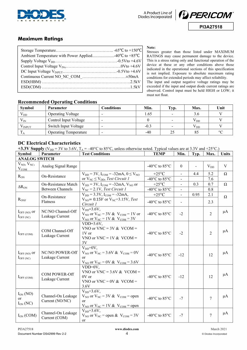
Maximum Ratings
Storage Temperature……………….………………….. -65 to +150 Ambient Temperature with Power Applied.....................-40 to +85 Supply Voltage VDD………………………………………-0.5Vto +4.6V Control Input Voltage VINx………………………………….0Vto +4.6V DC Input Voltage VINPUT…………………………………-0.5Vto +4.6V Continuous Current NO_NC_COM_……………………..……±50mA ESD(HBM) ……………………………………………………….2.5kV ESD(CDM) ……………………………………………………….1.5kV
Recommended Operating Conditions
Symbol Parameter Conditions Min. Typ. Max. Unit
VDD Operating Voltage - 1.65 - 3.6 V
VIN Control Input Voltage - 0 - VDD V
VINPUT Switch Input Voltage - -0.3 - VDD V
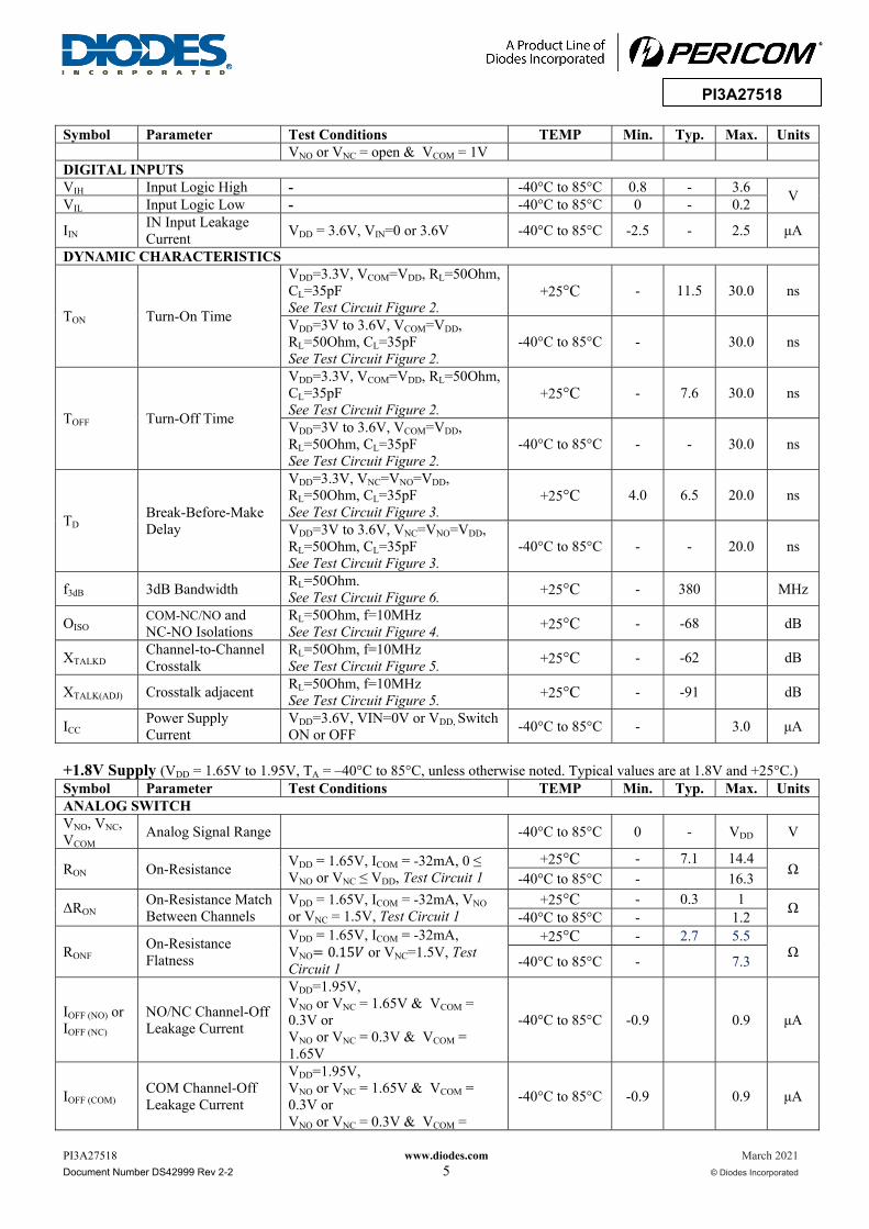
TA Operating Temperature - -40 25 85 °C DC Electrical Characteristics +3.3V Supply (VDD = 3V to 3.6V, TA = –40°C to 85°C, unless otherwise noted. Typical values are at 3.3V and +25°C.) Symbol Parameter Test Conditions TEMP Min. Typ. Max. Units ANALOG SWITCH VNO, VNC, VCOM
Analog Signal Range -40°C to 85°C 0 - VDD V
RON On-Resistance VDD = 3V, ICOM = -32mA, 0 ≤ VNO or VNC ≤ VDD, Test Circuit 1
+25°C - 4.4 5.2 Ω -40°C to 85°C - 7.6
ΔRON On-Resistance Match Between Channels
VDD = 3V, ICOM = -32mA, VNO or VNC = 2.1V, Test Circuit 1
+25°C - 0.3 0.7 Ω -40°C to 85°C - 0.8
RONF On-Resistance Flatness
VDD = 3.3V, ICOM = -32mA, VNO 0.15 or VNC=3.15V, Test Circuit 1
+25°C - 0.95 2.1 Ω -40°C to 85°C - 2.3
IOFF (NO) or IOFF (NC)
NC/NO Channel-Off Leakage Current
VDD=3.6V, VNO or VNC = 3V & VCOM = 1V or VNO or VNC = 1V & VCOM = 3V
-40°C to 85°C -2 2 μA
IOFF (COM) COM Channel-Off Leakage Current
VDD=3.6V, VNO or VNC = 3V & VCOM = 1V or VNO or VNC = 1V & VCOM = 3V
-40°C to 85°C -2 2 μA
IOFF (NO) or IOFF (NC)
NC/NO POWER-Off Leakage Current
VDD=0V, VNO or VNC = 3.6V & VCOM = 0V or VNO or VNC = 0V & VCOM = 3.6V
-40°C to 85°C -12 12 μA
IOFF (COM) COM POWER-Off Leakage Current
VDD=0V, VNO or VNC = 3.6V & VCOM = 0V or VNO or VNC = 0V & VCOM = 3.6V
-40°C to 85°C -12 12 μA
ION (NO) or ION (NC)
Channel-On Leakage Current (NO/NC)
VDD=3.6V, VNO or VNC = 3V & VCOM = open or VNO or VNC = 1V & VCOM = open
-40°C to 85°C -7 7 μA
ION (COM) Channel-On Leakage Current (COM)
VDD=3.6V, VNO or VNC = open & VCOM = 3V or
-40°C to 85°C -7 7 μA
Note: Stresses greater than those listed under MAXIMUM RATINGS may cause permanent damage to the device. This is a stress rating only and functional operation of the device at these or any other conditions above those indicated in the operational sections of this specification is not implied. Exposure to absolute maximum rating conditions for extended periods may affect reliability. The input and output negative voltage ratings may be exceeded if the input and output diode current ratings are observed. Control input must be held HIGH or LOW; it must not float.
PI3A27518 www.diodes.com March 2021
Document Number DS42999 Rev 2-2 5 © Diodes Incorporated
PI3A27518
Symbol Parameter Test Conditions TEMP Min. Typ. Max. Units VNO or VNC = open & VCOM = 1V
DIGITAL INPUTS VIH Input Logic High - -40°C to 85°C 0.8 - 3.6
V VIL Input Logic Low - -40°C to 85°C 0 - 0.2
IIN IN Input Leakage Current
VDD = 3.6V, VIN=0 or 3.6V -40°C to 85°C -2.5 - 2.5 μA
DYNAMIC CHARACTERISTICS
TON Turn-On Time
VDD=3.3V, VCOM=VDD, RL=50Ohm, CL=35pF See Test Circuit Figure 2.
+25°C - 11.5 30.0 ns
VDD=3V to 3.6V, VCOM=VDD, RL=50Ohm, CL=35pF See Test Circuit Figure 2.
-40°C to 85°C - 30.0 ns
TOFF Turn-Off Time
VDD=3.3V, VCOM=VDD, RL=50Ohm, CL=35pF See Test Circuit Figure 2.
+25°C - 7.6 30.0 ns
VDD=3V to 3.6V, VCOM=VDD, RL=50Ohm, CL=35pF See Test Circuit Figure 2.
-40°C to 85°C - - 30.0 ns
TD Break-Before-Make Delay
VDD=3.3V, VNC=VNO=VDD, RL=50Ohm, CL=35pF See Test Circuit Figure 3.
+25°C 4.0 6.5 20.0 ns
VDD=3V to 3.6V, VNC=VNO=VDD, RL=50Ohm, CL=35pF See Test Circuit Figure 3.
-40°C to 85°C - - 20.0 ns
f3dB 3dB Bandwidth RL=50Ohm. See Test Circuit Figure 6. +25°C - 380 MHz
OISO COM-NC/NO and NC-NO Isolations
RL=50Ohm, f=10MHz See Test Circuit Figure 4. +25°C - -68 dB
XTALKD Channel-to-Channel Crosstalk
RL=50Ohm, f=10MHz See Test Circuit Figure 5. +25°C - -62 dB
XTALK(ADJ) Crosstalk adjacent RL=50Ohm, f=10MHz See Test Circuit Figure 5. +25°C - -91 dB
ICC Power Supply Current
VDD=3.6V, VIN=0V or VDD, Switch ON or OFF
-40°C to 85°C - 3.0 μA
+1.8V Supply (VDD = 1.65V to 1.95V, TA = –40°C to 85°C, unless otherwise noted. Typical values are at 1.8V and +25°C.) Symbol Parameter Test Conditions TEMP Min. Typ. Max. Units ANALOG SWITCH VNO, VNC, VCOM
Analog Signal Range -40°C to 85°C 0 - VDD V
RON On-Resistance VDD = 1.65V, ICOM = -32mA, 0 ≤ VNO or VNC ≤ VDD, Test Circuit 1
+25°C - 7.1 14.4 Ω
-40°C to 85°C - 16.3
ΔRON On-Resistance Match Between Channels
VDD = 1.65V, ICOM = -32mA, VNO or VNC = 1.5V, Test Circuit 1
+25°C - 0.3 1 Ω
-40°C to 85°C - 1.2
RONF On-Resistance Flatness
VDD = 1.65V, ICOM = -32mA, VNO 0.15 or VNC=1.5V, Test Circuit 1
+25°C - 2.7 5.5 Ω
-40°C to 85°C - 7.3
IOFF (NO) or IOFF (NC)
NO/NC Channel-Off Leakage Current
VDD=1.95V, VNO or VNC = 1.65V & VCOM = 0.3V or VNO or VNC = 0.3V & VCOM = 1.65V
-40°C to 85°C -0.9 0.9 μA
IOFF (COM) COM Channel-Off Leakage Current
VDD=1.95V, VNO or VNC = 1.65V & VCOM = 0.3V or VNO or VNC = 0.3V & VCOM =
-40°C to 85°C -0.9 0.9 μA

PI3A27518 www.diodes.com March 2021
Document Number DS42999 Rev 2-2 6 © Diodes Incorporated
PI3A27518
Symbol Parameter Test Conditions TEMP Min. Typ. Max. Units 1.65V
IOFF (NO) or IOFF (NC)
NC/NO POWER-Off Leakage Current
VDD=0V, VNO or VNC = 1.95V & VCOM = 0V or VNO or VNC = 0V & VCOM = 1.95V
-40°C to 85°C -5 5 μA
IOFF (COM) COM POWER-Off Leakage Current
VDD=0V, VNO or VNC = 1.95V & VCOM = 0V or VNO or VNC = 0V & VCOM = 1.95V
-40°C to 85°C -5 5 μA
ION (NO) or ION (NC)
Channel-On Leakage Current (NO/NC)
VDD=1.95V, VNO or VNC = 1.65V &VCOM = open or VNO or VNC = 0.3V & VCOM = open
-40°C to 85°C -5.2 5.2 μA
ION (COM) Channel-On Leakage Current (COM)
VDD=1.95V, VNO or VNC = open & VCOM = 1.65V or VNO or VNC = open & VCOM = 0.3V
-40°C to 85°C -5.2 5.2 μA
DIGITAL INPUTS VIH Input Logic High - -40°C to 85°C 0.8 - 1.95
V VIL Input Logic Low - -40°C to 85°C 0 - 0.2
IIN IN Input Leakage Current
VDD = 1.95V, VIN=0 or 1.95V -40°C to 85°C -2.1 - 2.1 μA
DYNAMIC CHARACTERISTICS
TON Turn-On Time VDD=1.65V to 1.95V, VCOM=VDD, RL=50Ohm, CL=35pF See Test Circuit Figure 2.
+25°C - 18.9 45 ns
-40°C to 85°C - - 45
TOFF Turn-Off Time VDD=1.65V to 1.95V, VCOM=VDD, RL=50Ohm, CL=35pF See Test Circuit Figure 2.
+25°C - 14.0 26 ns
-40°C to 85°C - - 26
TD Break-Before-Make Delay
VDD=1.65V to 1.95V, VCOM=VDD, RL=50Ohm, CL=35pF See Test Circuit Figure 3.
+25°C 5.3 11.8 40 ns
-40°C to 85°C - - 40
f3dB 3dB Bandwidth RL=50Ohm. See Test Circuit Figure 6. +25°C - 380 - MHz
OISO COM-NC/NO and NC-NO Isolations
RL=50Ohm, f=10MHz See Test Circuit Figure 4. +25°C - -66.0 - dB
XTALKD Channel-to-Channel Crosstalk
RL=50Ohm, f=10MHz See Test Circuit Figure 5. +25°C - -60.0 - dB
XTALK(ADJ) Crosstalk adjacent RL=50Ohm, f=10MHz See Test Circuit Figure 5. +25°C - -91.0 - dB
ICC Power Supply Current
VDD=1.95V, VIN=0V or VDD,
Switch ON or OFF -40°C to 85°C - - 1.5 μA
Capacitance Symbol Parameter Test Conditions Min. Typ. Max. Units CNC (OFF), CNO (OFF)
NC/NO Off Capacitance
VNC or VNO = VDD or GND, Switch OFF f = 1MHz, See Test Circuit Figure 7.
- 10 -
pF CCOM (OFF)
COM Off Capacitance
VCOM = VDD or GND, Switch OFF f = 1MHz, See Test Circuit Figure 7.
- 16 -
CNC (ON), CNO (ON)
NC/NO On Capacitance
VNC or VNO = VDD or GND, Switch ON f = 1MHz, See Test Circuit Figure 8.
- 21.5 -
CCOM (ON) COM On Capacitance
VCOM = VDD or GND, Switch ON f = 1MHz, See Test Circuit Figure 8.
- 21.5 -
CIN Digital Input Capacitance
f = 1MHz - 3 - pF

PI3A27518 www.diodes.com March 2021
Document Number DS42999 Rev 2-2 7 © Diodes Incorporated
PI3A27518
Test Circuits and Timing Diagrams
Figure 1. ON Resistance Notes: 1. Unused input (NC or NO) must be grounded.
Figure 2. Switching Times
Figure 3. Break Before Make Interval Timing
VDD VDD NO
NC
VDD

PI3A27518 www.diodes.com March 2021
Document Number DS42999 Rev 2-2 8 © Diodes Incorporated
PI3A27518
Figure 4. OFF Isolation (OISO)
Figure 5. Channel-to-Channel Crosstalk
Figure 6. Bandwidth

PI3A27518 www.diodes.com March 2021
Document Number DS42999 Rev 2-2 9 © Diodes Incorporated
PI3A27518
Figure 7. Channel Off Capacitance
Figure 8. Channel On Capacitance
Part Marking Top mark not available at this time. To obtain advance information regarding the top mark, please contact your local sales representative.

PI3A27518 www.diodes.com March 2021
Document Number DS42999 Rev 2-2 10 © Diodes Incorporated
PI3A27518
Packaging Mechanical 24-TQFN (ZD)
For latest package info. please check: http://www.diodes.com/design/support/packaging/pericom-packaging/packaging-mechanicals-and-thermal-characteristics/ Ordering Information
Part Number Packaging Code Package Description PI3A27518ZDEX ZD 24-Contact, Very Thin Quad Flat No-Lead (TQFN)
Notes: 1. No purposely added lead. Fully EU Directive 2002/95/EC (RoHS), 2011/65/EU (RoHS 2) & 2015/863/EU (RoHS 3) compliant. 2. See https://www.diodes.com/quality/lead-free/ for more information about Diodes Incorporated’s definitions of Halogen- and Antimony-free, "Green" and
Lead-free. 3. Halogen- and Antimony-free "Green” products are defined as those which contain <900ppm bromine, <900ppm chlorine (<1500ppm total Br + Cl) and
<1000ppm antimony compounds. 4. E = Pb-free and Green 5. X suffix = Tape/Reel

PI3A27518 www.diodes.com March 2021
Document Number DS42999 Rev 2-2 11 © Diodes Incorporated
PI3A27518
IMPORTANT NOTICE
1. DIODES INCORPORATED AND ITS SUBSIDIARIES (“DIODES”) MAKE NO WARRANTY OF ANY KIND, EXPRESS OR IMPLIED, WITH REGARDS TO ANY INFORMATION CONTAINED IN THIS DOCUMENT, INCLUDING, BUT NOT LIMITED TO, THE IMPLIED WARRANTIES OF MERCHANTABILITY, FITNESS FOR A PARTICULAR PURPOSE OR NON-INFRINGEMENT OF THIRD PARTY INTELLECTUAL PROPERTY RIGHTS (AND THEIR EQUIVALENTS UNDER THE LAWS OF ANY JURISDICTION). 2. The Information contained herein is for informational purpose only and is provided only to illustrate the operation of Diodes products described herein and application examples. Diodes does not assume any liability arising out of the application or use of this document or any product described herein. This document is intended for skilled and technically trained engineering customers and users who design with Diodes products. Diodes products may be used to facilitate safety-related applications; however, in all instances customers and users are responsible for (a) selecting the appropriate Diodes products for their applications, (b) evaluating the suitability of the Diodes products for their intended applications, (c) ensuring their applications, which incorporate Diodes products, comply the applicable legal and regulatory requirements as well as safety and functional-safety related standards, and (d) ensuring they design with appropriate safeguards (including testing, validation, quality control techniques, redundancy, malfunction prevention, and appropriate treatment for aging degradation) to minimize the risks associated with their applications. 3. Diodes assumes no liability for any application-related information, support, assistance or feedback that may be provided by Diodes from time to time. Any customer or user of this document or products described herein will assume all risks and liabilities associated with such use, and will hold Diodes and all companies whose products are represented herein or on Diodes’ websites, harmless against all damages and liabilities. 4. Products described herein may be covered by one or more United States, international or foreign patents and pending patent applications. Product names and markings noted herein may also be covered by one or more United States, international or foreign trademarks and trademark applications. Diodes does not convey any license under any of its intellectual property rights or the rights of any third parties (including third parties whose products and services may be described in this document or on Diodes’ website) under this document. 5. Diodes products are provided subject to Diodes’ Standard Terms and Conditions of Sale (https://www.diodes.com/about/company/terms-and-conditions/terms-and-conditions-of-sales/) or other applicable terms. This document does not alter or expand the applicable warranties provided by Diodes. Diodes does not warrant or accept any liability whatsoever in respect of any products purchased through unauthorized sales channel. 6. Diodes products and technology may not be used for or incorporated into any products or systems whose manufacture, use or sale is prohibited under any applicable laws and regulations. Should customers or users use Diodes products in contravention of any applicable laws or regulations, or for any unintended or unauthorized application, customers and users will (a) be solely responsible for any damages, losses or penalties arising in connection therewith or as a result thereof, and (b) indemnify and hold Diodes and its representatives and agents harmless against any and all claims, damages, expenses, and attorney fees arising out of, directly or indirectly, any claim relating to any noncompliance with the applicable laws and regulations, as well as any unintended or unauthorized application. 7. While efforts have been made to ensure the information contained in this document is accurate, complete and current, it may contain technical inaccuracies, omissions and typographical errors. Diodes does not warrant that information contained in this document is error-free and Diodes is under no obligation to update or otherwise correct this information. Notwithstanding the foregoing, Diodes reserves the right to make modifications, enhancements, improvements, corrections or other changes without further notice to this document and any product described herein. This document is written in English but may be translated into multiple languages for reference. Only the English version of this document is the final and determinative format released by Diodes. 8. Any unauthorized copying, modification, distribution, transmission, display or other use of this document (or any portion hereof) is prohibited. Diodes assumes no responsibility for any losses incurred by the customers or users or any third parties arising from any such unauthorized use. Copyright © 2021 Diodes Incorporated www.diodes.com