
Micro-light-emitting diodes with quantum dots in ... - Nature
Upload
khangminh22Category
view
0download
0
ISBN 978-82-326- 4072-0 (printed ver.)ISBN 978-82-326- 4073-7 (electronic ver.)
ISSN 1503-8181
Doctoral theses at NTNU, 2019:238
Subhadra Tiwari
SiC MOSFETs and Diodes:Characterization, Applicationsand Low-Inductive ConverterDesign Considerations
Doc
tora
l the
sis
Doctoral theses at N
TNU
, 2019:238Subhadra Tiw
ari
NTN
UN
orw
egia
n U
nive
rsity
of S
cien
ce a
nd T
echn
olog
yTh
esis
for
the
Deg
ree
ofP
hilo
soph
iae
Doc
tor
Facu
lty
of In
form
atio
n Te
chno
logy
and
Ele
ctri
cal
Engi
neer
ing
Dep
artm
ent o
f Ele
ctri
c P
ower
Eng
inee
ring

Thesis for the Degree of Philosophiae Doctor
Trondheim, April 2019
Norwegian University of Science and TechnologyFaculty of Information Technology and Electrical EngineeringDepartment of Electric Power Engineering
Subhadra Tiwari
SiC MOSFETs and Diodes:Characterization, Applications andLow-Inductive Converter DesignConsiderations

NTNUNorwegian University of Science and Technology
Thesis for the Degree of Philosophiae Doctor
Faculty of Information Technology and Electrical EngineeringDepartment of Electric Power Engineering
© Subhadra Tiwari
ISBN 978-82-326- 4072-0 (printed ver.)ISBN 978-82-326- 4073-7 (electronic ver.)ISSN 1503-8181
Doctoral theses at NTNU, 2019:238
Printed by NTNU Grafisk senter

To my parents


Preface
This thesis is submitted to the Norwegian University of Science and Technology (NTNU)in partial fulfillment of the requirements for the degree of philosophiae doctor (PhD).
The research is carried out at the Department of Electric Power Engineering, Faculty ofInformation Technology and Electrical Engineering, NTNU, Norway. The PhD work issponsored by The Research Council of Norway, and six industry partners: EFD Induction,Siemens, Eltek, Norwegian Electric Systems, and Vacon.
Trondheim, April 2019Subhadra Tiwari
i

ii

Acknowledgments
I would like to express my sincere gratitude to my main supervisor Prof. Ole-MortenMidtgard for providing me with this great opportunity, and for his supervision, continuousencouragement and support. My sincere thanks to my co-supervisor Prof. em. ToreMarvin Undeland for his supervision, invaluable insight, helpful feedback and intriguingquestions throughout this research work.
I would also like to thank EFD Induction AS, which is one of the industry partnersfinancing this PhD project, for providing me the opportunity to work in their laboratory.Special thanks goes to John Kare Langelid, from EFD Induction AS, for sharing hisexperience, knowledge and providing valuable comments, and suggestions throughoutthis PhD work. I also wish to acknowledge Prof. Roy Nilsen, Dr. Supratim Basu,Dr. Richard Lund, and Dr. Ibrahim Abed Abuishmais for their valuable inputs andsuggestions. I would also like to thank Terje Rogne from The Switch Marine Drive AS,and Kjell Ljøkelsøy from SINTEF Energy Research for providing technical feedbacks forsome of my papers. My thanks to Ali Rabiei from Chalmers University of Technology fortechnical discussions during his visit to NTNU.
I would like to thank Prof. Rik W. De Doncker for providing me the opportunityto work at E. ON Energy Research Center for six months as a guest PhD researcherat RWTH Aachen University. Moreover, I had the opportunity to visit CPES lab atVirginia Polytechnic Institute for two weeks in 2016. Both of these international exposuresenhanced my knowledge of the laboratory and simulation tools that were central for myPhD project.
The Department of Electric Power Engineering at NTNU has provided good labo-ratory facilities and great administrative support. My thanks to the members of staffat the department for help regarding various practical matters. Additionally, the socialenvironment among the fellow PhD students has been of great value. I would also liketo thank my office mates, Ole Christian Spro and Andreas Giannakis for their friendlychats.
Finally, I would like to thank my family. They have always supported and believedin me, and words cannot express how truly appreciative I am for all of their love and en-couragement. Last but not least, my husband Raghbendra deserves my deepest gratitudefor his support and love during my years as a PhD student. Thanks also for your helpin reading the draft of my dissertation. Moreover, it is impossible not to mention mybeloved son, Ayan. He is the true source of motivation and energy for me.
Trondheim, April 2019Subhadra Tiwari
iii

iv

Abstract
The future power electronic system trends are: higher efficiency, higher power density,higher operating temperature and lower operation cost of power electronic converters. Theemerging wide-bandgap (WBG) semiconductor material, especially silicon carbide (SiC),exhibits outstanding inherent properties that promise the potential to meet the subsequentgrowing demands. SiC enables the development of power devices capable of switchingefficiently even at higher voltages and temperatures compared to the matured and well-established Si technology of today. Nonetheless, parasitic inductance and capacitance inthe switching circuit are limitations for fully unleashing the fast-switching potential ofthese devices. The objective of this research is to evaluate what the state-of-the-art SiCdevices, particularly SiC MOSFETs, offer at present and what can be done for betterrealizing their high switching-speed capability.
First, to assess the fast dynamic characteristics of SiC devices with a high degree ofaccuracy, measurement probes and oscilloscope with adequate bandwidth along with low-inductive connections are adopted. Switching characterization was conducted via double-pulse test in hard-switched as well as in resonant topology. Based on the measurementresults, it is recommended to use a realistic topology for the precise assessment of switchinglosses in SiC devices.
Second, the state-of-the-art SiC MOSFET modules are examined to determine howfast they switch compared to the class-leading IGBT modules, given that they are pack-aged in the standard plastic housing. Measurement results revealed that the maximumdv/dt and di/dt rates that SiC MOSFET achieves are: 20 V/ns and 11 A/ns at 600 Vbus voltage and 120 A load current. Si IGBT, on the other hand, achieved 17 V/nsand 12 A/ns when switched at similar conditions. According to this result, it can beinferred that dv/dt and di/dt rates that SiC MOSFET reaches are not as revolutionaryas its intrinsic properties can potentially offer. In fact, this outcome can be attributed tothe higher internal gate resistance that manufacturers use for avoiding oscillation duringturn-off and the higher package inductance. In order to know what else can be achievedusing SiC MOSFET, the body-diodes of the state-of-the-art SiC MOSFETs (both planarand trench technologies) were inspected. A particular focus was put on di/dt during thesecond-half of the recovery, keeping di/dt on the first-half of the recovery constant for allthe devices being tested. Experimental outcomes revealed that the body-diodes in newgeneration SiC MOSFETs are as good as SiC junction barrier Schottky (JBS) diodes fromthe switching point of view. Nonetheless, the forward voltage drop is higher approximatelyby a factor of 3 compared to unipolar SiC Schottky diodes. Based on this informationand the research conducted by another team, which confirmed that the body-diodes innew SiC MOSFETs do not create reliability issues anymore like those seen in the initialgeneration SiC MOSFETs, it is concluded that the body-diodes in SiC MOSFETs workeffectively as freewheeling diodes.
v

Third, SiC MOSFETs are evaluated in three different key applications. One of thoseapplications is a 240 kW back-to-back connected three-phase, two-level voltage sourceconverter for motor drive, which disclosed that, for the same converter power loss, theswitching frequency in an all-SiC-based converter can be increased by six times comparedto that of an all-Si-based converter. Another application is an 80 kW single-phase, full-bridge inverter for induction heating applications, which proved an efficiency of 99.3%when switched at 200 kHz. SiC DioMOS, where MOSFET and diode are fabricated ina single chip, was the device under test and the inverter loss was measured via calori-metric method in this case. Finally, a 1 kW power factor correction rectifier is evaluatedemploying SiC MOSFET and SiC JBS diode in boost stage. A peak efficiency of 97.2%was achieved when switched at 250 kHz satisfying the 80 PLUS regulation throughoutthe entire load range. Moreover, EMI measurements revealed that the rectifier satisfiesCISPR 11 Class B limits. Furthermore, when the switching frequency was increased from66 to 250 kHz, the size of boost inductor was reduced drastically, while the emissions wereincreased by roughly 10 dB throughout the entire conducted spectra for the identical sizeof EMI filter.
To further unlock the fast switching potential of SiC devices, low-inductive converterdesign guidelines are proposed, such as the selection of DC-clamping capacitors withlow internal inductance and their appropriate orientation and stripline layouts wheneverpossible maintaining width to length ratio larger than unity. Two design examples forfurther achieving low switching loop inductance with SiC modules and discrete SiC devicesare provided. For the SiC modules, multiple DC-source busbars for multiple screw holemodules are recommended. As internal inductance of the standard module is larger, anexample of layout employing seven-pin discrete SiC MOSFETs and Ceralink capacitorsis designed, the switching loop inductance of which is estimated to be 5 nH via 3D FEMsimulations.
Keywords: Silicon Carbide (SiC), Metal-Oxide-Semiconductor Field-Effect Transis-tor (MOSFET), Junction Barrier Schottky (JBS) diodes, High-Efficiency Converters, Lowinductance designs.
vi

Contents
Preface i
Acknowledgments iii
Abstract v
Table of Contents vii
List of Tables xii
List of Figures xiii
List of Symbols xxv
1 Introduction 11.1 Background and motivation . . . . . . . . . . . . . . . . . . . . . . . . . . 11.2 Scope of the work . . . . . . . . . . . . . . . . . . . . . . . . . . . . . . . . 21.3 Structure of the thesis . . . . . . . . . . . . . . . . . . . . . . . . . . . . . 31.4 Methodology . . . . . . . . . . . . . . . . . . . . . . . . . . . . . . . . . . 31.5 Main scientific contributions . . . . . . . . . . . . . . . . . . . . . . . . . . 41.6 Overview of publications . . . . . . . . . . . . . . . . . . . . . . . . . . . . 6
1.6.1 List of journal papers . . . . . . . . . . . . . . . . . . . . . . . . . . 61.6.2 List of conference papers . . . . . . . . . . . . . . . . . . . . . . . . 61.6.3 List of tutorial presentations . . . . . . . . . . . . . . . . . . . . . . 7
2 Silicon carbide power devices and key advantages and challenges 92.1 Material properties . . . . . . . . . . . . . . . . . . . . . . . . . . . . . . . 92.2 Fundamentals and potential advantages of SiC . . . . . . . . . . . . . . . . 10
2.2.1 Fundamental properties of SiC . . . . . . . . . . . . . . . . . . . . . 102.2.2 Potential advantages of SiC . . . . . . . . . . . . . . . . . . . . . . 10
2.3 Overview of SiC power devices . . . . . . . . . . . . . . . . . . . . . . . . . 122.3.1 SiC power diodes . . . . . . . . . . . . . . . . . . . . . . . . . . . . 122.3.2 SiC switches . . . . . . . . . . . . . . . . . . . . . . . . . . . . . . . 14
2.4 Comparison of SiC MOSFETs/SiC diodes with Si MOSFETs/Si diodes . . 172.4.1 Structures of MOSFET . . . . . . . . . . . . . . . . . . . . . . . . . 172.4.2 Comparison of SiC MOSFETs with Si MOSFETs . . . . . . . . . . 172.4.3 Structures of diode . . . . . . . . . . . . . . . . . . . . . . . . . . . 192.4.4 Comparison of SiC diodes with Si diodes . . . . . . . . . . . . . . . 19
2.5 Packaging . . . . . . . . . . . . . . . . . . . . . . . . . . . . . . . . . . . . 20
vii

2.6 Critical thinking or challenges . . . . . . . . . . . . . . . . . . . . . . . . . 212.7 Summary . . . . . . . . . . . . . . . . . . . . . . . . . . . . . . . . . . . . 22
3 Prerequisites for accurate assessment of switching loss by electricalmethod 233.1 Introduction . . . . . . . . . . . . . . . . . . . . . . . . . . . . . . . . . . . 233.2 Prerequisites for accurate measurement of high-speed switching signals . . 24
3.2.1 Bandwidth of measuring probes and oscilloscope . . . . . . . . . . . 243.2.2 Low-inductive measurement connections . . . . . . . . . . . . . . . 253.2.3 Load inductor characteristics . . . . . . . . . . . . . . . . . . . . . 263.2.4 Post processing of measured data . . . . . . . . . . . . . . . . . . . 26
3.3 Importance of realistic circuits for loss evaluation . . . . . . . . . . . . . . 273.3.1 Hard-switched topology . . . . . . . . . . . . . . . . . . . . . . . . 283.3.2 Resonant inverter topology . . . . . . . . . . . . . . . . . . . . . . . 293.3.3 Experimental results for hard versus resonant topology . . . . . . . 29
3.4 Summary . . . . . . . . . . . . . . . . . . . . . . . . . . . . . . . . . . . . 31
4 Characterization of state-of-the-art SiC MOSFET modules 334.1 Introduction . . . . . . . . . . . . . . . . . . . . . . . . . . . . . . . . . . . 334.2 Comparison of SiC MOSFET modules . . . . . . . . . . . . . . . . . . . . 34
4.2.1 Modules with different stray inductance . . . . . . . . . . . . . . . 344.2.2 Modules with different stray capacitance . . . . . . . . . . . . . . . 39
4.3 Comparison of SiC MOSFET and Si IGBT . . . . . . . . . . . . . . . . . . 424.3.1 SiC MOSFET vs. Si non-punch-through IGBT modules . . . . . . . 424.3.2 SiC MOSFET versus Si soft-punch-through IGBT . . . . . . . . . . 46
4.4 Summary . . . . . . . . . . . . . . . . . . . . . . . . . . . . . . . . . . . . 51
5 Characterization of body-diodes in state-of-the-art SiC MOSFETs 535.1 Introduction . . . . . . . . . . . . . . . . . . . . . . . . . . . . . . . . . . . 535.2 Device under test . . . . . . . . . . . . . . . . . . . . . . . . . . . . . . . . 545.3 Methodology . . . . . . . . . . . . . . . . . . . . . . . . . . . . . . . . . . 555.4 Hardware setup and measurement considerations . . . . . . . . . . . . . . 565.5 Experimental results . . . . . . . . . . . . . . . . . . . . . . . . . . . . . . 57
5.5.1 Planar versus double-trench MOSFETs . . . . . . . . . . . . . . . . 575.5.2 Planar Schottky diodes with different chip areas . . . . . . . . . . . 585.5.3 Trench cascode JFET . . . . . . . . . . . . . . . . . . . . . . . . . . 605.5.4 Comparison of DUTs at 400 and 600V . . . . . . . . . . . . . . . . 61
5.6 Conclusion . . . . . . . . . . . . . . . . . . . . . . . . . . . . . . . . . . . . 63
6 Applications of SiC power devices 656.1 Wind power applications . . . . . . . . . . . . . . . . . . . . . . . . . . . . 66
6.1.1 Methodology and measurement results . . . . . . . . . . . . . . . . 666.1.2 Topology selection and simulation of losses . . . . . . . . . . . . . . 676.1.3 Simulation results . . . . . . . . . . . . . . . . . . . . . . . . . . . . 686.1.4 Evaluation of inverter power loss at different switching frequencies . 716.1.5 Evaluation of back-to-back converter efficiency at different switch-
ing frequencies . . . . . . . . . . . . . . . . . . . . . . . . . . . . . 726.1.6 Discussion and summary . . . . . . . . . . . . . . . . . . . . . . . . 72
viii

6.2 Induction heating applications . . . . . . . . . . . . . . . . . . . . . . . . . 746.2.1 Device under study . . . . . . . . . . . . . . . . . . . . . . . . . . . 756.2.2 Calorimetric loss measurement in a full-bridge resonant inverter . . 776.2.3 Accuracy analysis of calorimetric efficiency measurement . . . . . . 816.2.4 Discussion and summary . . . . . . . . . . . . . . . . . . . . . . . . 82
6.3 Power factor correction applications . . . . . . . . . . . . . . . . . . . . . . 836.3.1 Converter description and specification . . . . . . . . . . . . . . . . 846.3.2 PFC converter loss evaluation via circuit simulation . . . . . . . . . 866.3.3 Circuit design and layout considerations of PFC rectifier . . . . . . 896.3.4 Experimental results . . . . . . . . . . . . . . . . . . . . . . . . . . 926.3.5 Summary and conclusion . . . . . . . . . . . . . . . . . . . . . . . . 95
7 Low-inductive converter design considerations 977.1 Introduction . . . . . . . . . . . . . . . . . . . . . . . . . . . . . . . . . . . 977.2 Theoretical background for the selection of dielectric material . . . . . . . 997.3 Impact of geometry on stray inductance and capacitance . . . . . . . . . . 1007.4 Selection of low inductance DC-link capacitors . . . . . . . . . . . . . . . . 1017.5 Impact of capacitor orientation on inductance . . . . . . . . . . . . . . . . 103
7.5.1 Axial terminated capacitors . . . . . . . . . . . . . . . . . . . . . . 1037.5.2 Circular terminated capacitors . . . . . . . . . . . . . . . . . . . . . 106
7.6 Design of DC-link for AC-DC-AC converter . . . . . . . . . . . . . . . . . 1087.6.1 Sizing the DC-link capacitor . . . . . . . . . . . . . . . . . . . . . . 1087.6.2 Comparison of stray inductance shared by various parts . . . . . . . 1087.6.3 Exemplifying a DC-link busbar design with coaxial capacitor . . . . 110
7.7 Example of a low-inductive busbar design for SiC MOSFET modules . . . 1117.7.1 Busbar for single screw hole module . . . . . . . . . . . . . . . . . 1117.7.2 Busbar for multiple screw holes module . . . . . . . . . . . . . . . 112
7.8 Example of a low-inductive busbar design using discrete SiC MOSFETs . . 1137.9 Conclusion . . . . . . . . . . . . . . . . . . . . . . . . . . . . . . . . . . . . 114
8 Conclusions and Future work 1178.1 Summary and conclusions . . . . . . . . . . . . . . . . . . . . . . . . . . . 1178.2 Suggested future work . . . . . . . . . . . . . . . . . . . . . . . . . . . . . 121
Appendix A LTSpice Simulation for analyzing the impact of parasitics inthe switching 123A.1 Impact of stray inductance . . . . . . . . . . . . . . . . . . . . . . . . . . . 123
A.1.1 Impact of switching-loop inductance . . . . . . . . . . . . . . . . . 123A.1.2 Impact of gate-loop inductance . . . . . . . . . . . . . . . . . . . . 124
A.2 Impact of stray capacitance . . . . . . . . . . . . . . . . . . . . . . . . . . 125A.2.1 Impact of gate-source capacitance . . . . . . . . . . . . . . . . . . . 125A.2.2 Impact of drain-source capacitance . . . . . . . . . . . . . . . . . . 126A.2.3 Impact of gate-drain capacitance . . . . . . . . . . . . . . . . . . . 127
Appendix B 3D FEM simulation for low inductive circuit designs 129B.1 Modelling of busbar in Ansys Q3D extractor . . . . . . . . . . . . . . . . 129B.2 Estimation of stray inductance via measurement and analytical expression 132
ix

Appendix C Fundamental information for Chapter 6 133C.1 Equations for passive component sizing . . . . . . . . . . . . . . . . . . . . 133C.2 Equations for conduction loss calculation . . . . . . . . . . . . . . . . . . . 133C.3 A complete schematic diagram and component layout of PFC rectifier (two-
layer board) . . . . . . . . . . . . . . . . . . . . . . . . . . . . . . . . . . 134
Appendix D An insight into close-to-lossless switching enabled by SiCMOSFET 137D.1 Introduction . . . . . . . . . . . . . . . . . . . . . . . . . . . . . . . . . . . 137D.2 Design of low inductive layout via 3D FEM simulation in Ansys Q3D . . . 138D.3 Evaluation of inverter via LTSpice simulations . . . . . . . . . . . . . . . . 141
D.3.1 Analysis of voltage overshoot when switched at 8 A . . . . . . . . . 142D.3.2 Analysis of voltage overshoot when switched at 15 A . . . . . . . . 143D.3.3 Conclusion . . . . . . . . . . . . . . . . . . . . . . . . . . . . . . . . 144
Bibliography 145
x

List of Tables
2.1 Key material properties of Si, GaAs, SiC and GaN [14,31]. . . . . . . . . 9
2.2 A list of reported SiC BJTs. . . . . . . . . . . . . . . . . . . . . . . . . . . 16
2.3 A list of reported SiC IGBTs. . . . . . . . . . . . . . . . . . . . . . . . . . 17
2.4 Comparison of key parameters for Si versus SiC MOSFETs in TO247 package. 18
2.5 Comparison of key parameters for Si- versus SiC Schottky diodes in TO247package. . . . . . . . . . . . . . . . . . . . . . . . . . . . . . . . . . . . . . 20
2.6 Commercially available SiC modules and their package inductance. . . . . 21
3.1 Data sheet readings of voltage measurement probes used in the thesis. . . . 25
3.2 Current measurement techniques and their specifications as per data sheet. 25
4.1 On-state resistance, total die size, Ciss, and Coss of the modules understudy. . . . . . . . . . . . . . . . . . . . . . . . . . . . . . . . . . . . . . . 35
4.2 Summary of laboratory measurements for CAS120M12BM2 (Wolfspeed,MOSFET). . . . . . . . . . . . . . . . . . . . . . . . . . . . . . . . . . . . 36
4.3 Summary of laboratory measurements for BSM120D12P2C005 (Rohm,MOSFET). . . . . . . . . . . . . . . . . . . . . . . . . . . . . . . . . . . . 36
4.4 Data sheet readings of SiC MOSFET dies with different voltage ratings. . . 39
4.5 Data sheet readings of SiC MOSFET modules with same voltage ratings. . 39
4.6 Key electrical parameters of SiC MOSFET versus Si NPT IGBT modules. 43
4.7 Summary of laboratory measurements for CAS300M12BM2 (Wolfspeed,MOSFET). . . . . . . . . . . . . . . . . . . . . . . . . . . . . . . . . . . . 43
4.8 Summary of laboratory measurements for SKM400GB125D (Semikron,IGBT). . . . . . . . . . . . . . . . . . . . . . . . . . . . . . . . . . . . . . . 44
4.9 Specific loss of SiC MOSFET versus Si IGBT for the selected Rg,on andRg,off . . . . . . . . . . . . . . . . . . . . . . . . . . . . . . . . . . . . . . . 45
4.10 Key electrical parameters of SiC MOSFET versus Si SPT IGBT modules. 47
4.11 Key measurements of SiC MOSFET vs Si IGBT module. Vds = 500 V, Ids= 120 A, two different junction temperatures: Tj = 25 C and Tj = 125 C,and two different gate resistances for each modules. . . . . . . . . . . . . . 50
5.1 Key parameters of the investigated device under test. . . . . . . . . . . . . 54
5.2 dv/dt, di/dt2, Irrm, and trr of C4D and SCS at 20 A and two differentvoltages: 100 and 400 V. . . . . . . . . . . . . . . . . . . . . . . . . . . . 60
5.3 dv/dt, di/dt2, Irrm, and trr of the investigated DUTs at 400 V and 600 Vwhile keeping a constant di/dt1 of 1.2 A/ns. Compared to 400 V, dv/dt,Irrm, and trr are measured to be higher at 600 V. . . . . . . . . . . . . . . 62
xi

6.1 Key electrical parameters of half-bridge SiC MOSFET module versus half-bridge Si NPT IGBT module. . . . . . . . . . . . . . . . . . . . . . . . . . 66
6.2 Reading of currents and energy losses (refer Fig. 6.4 (a) and (b). . . . . . . 696.3 A comparison of simulated and numerically calculated power loss of tran-
sistor T1. . . . . . . . . . . . . . . . . . . . . . . . . . . . . . . . . . . . . 706.4 Definition of symbols used in (6.1) - (6.3). . . . . . . . . . . . . . . . . . . 706.5 Key electrical parameters of the six-pack SiC MOSFET module versus the
six-pack Si SPT IGBT module. . . . . . . . . . . . . . . . . . . . . . . . . 736.6 Conduction losses of SiC MOSFET versus Si IGBT modules (six-packs)
in a two-level VSC during motoring versus generating operations at twodifferent junction temperatures. . . . . . . . . . . . . . . . . . . . . . . . . 73
6.7 Conduction losses of SiC MOSFET versus Si IGBT modules (half-bridges)in a two-level VSC during motoring versus generating operations at twodifferent junction temperatures. . . . . . . . . . . . . . . . . . . . . . . . . 74
6.8 Major differences between a SiC DioMOS and a standard SiC MOSFETmodules. . . . . . . . . . . . . . . . . . . . . . . . . . . . . . . . . . . . . . 75
6.9 Summary of the measured parameters at 78 kW input power. . . . . . . . 806.10 Summary of the calculated parameters for approximately 78 kW of input
power. . . . . . . . . . . . . . . . . . . . . . . . . . . . . . . . . . . . . . . 816.11 Summary of the specific turn-off loss measurements in three different
topologies and normalization with regard to electrically measured loss in ahalf-bridge resonant inverter. . . . . . . . . . . . . . . . . . . . . . . . . . . 82
6.12 Specifications of PFC boost converter. . . . . . . . . . . . . . . . . . . . . 856.13 Chosen components with their part numbers and specifications. The on-
state parameters associated with the diode, VFO and Rd, and MOSFET,RDS,on, are taken at 125 C [82,86]. . . . . . . . . . . . . . . . . . . . . . . 86
6.14 EMI filter specifications. . . . . . . . . . . . . . . . . . . . . . . . . . . . . 92
7.1 List of insulating materials with breakdown voltage, dielectric constant andcontinuous temperature. . . . . . . . . . . . . . . . . . . . . . . . . . . . . 99
7.2 Electrical specification of low inductance DC-link capacitors. . . . . . . . . 1027.3 Parameters normalized to capacitance of Ring capacitor. . . . . . . . . . . 1027.4 Parameters normalized to ripple current of Ring capacitor. . . . . . . . . . 1027.5 Summary of inductances for axial terminated capacitors. . . . . . . . . . . 1057.6 Summary of inductances for circular terminated capacitors. . . . . . . . . . 1077.7 Summary of switching loop inductance. . . . . . . . . . . . . . . . . . . . . 1097.8 Summary of Lstray,ext in different designs from Q3D simulation. . . . . . . 113
xii

List of Figures
2.1 Key applications benefiting from SiC power devices. . . . . . . . . . . . . . 112.2 An overview of SiC power devices. . . . . . . . . . . . . . . . . . . . . . . . 132.3 Structures of planar (left) and double-trench, gate-source-trench (right),
MOSFETs. Note that trench structures improve the static performancesin MOSFETs [46,47]. . . . . . . . . . . . . . . . . . . . . . . . . . . . . . . 18
2.4 Structures of planar (left) and trench (right) SBD. . . . . . . . . . . . . . . 19
3.1 For Rg,ext = 0 Ω, the trise and tfall are in the range of 20 ns and the ringingfrequency (fosc) is 30 MHz, thus the probes and oscilloscope bandwidthof ≥ 150 MHz are adequate for tracking these switching transients. Thelegends used in Fig. 3.1 are: Vds, drain-source voltage; Ids, drain-sourcecurrent; and Vgs, gate-source voltage. . . . . . . . . . . . . . . . . . . . . . 24
3.2 (a) Laboratory setup showing the arrangement for low-inductive connec-tions for current and voltage measurements of the device under test. Thecurrent is measured by a high-bandwidth, low-inductive current shunt,and the voltage is measured by a high-bandwidth single-ended probe withprobe-tip adapter as displayed. (b) Illustration of a typical ground-leadof a voltage probe (Case 1) versus probe-tip adapter connection (Case 2).Load current is measured by a dc/ac current probe out of a 40-turn ferritecore transformer. . . . . . . . . . . . . . . . . . . . . . . . . . . . . . . . . 26
3.3 Turn-off transients during hard-switching together with the power wave-forms. Fig. (a) illustrates the influence of probe delay. With 14 ns ofvoltage probe delay with respect to current measured by shunt, there isa significant difference in the computed energy loss. Fig. (b) exposes theinfluence of integration limits on the power curve. Given that there areoscillations, the choice of the end of the integration time is not clear. tAdenotes the start of the integration time, while tB and tC are two optionsto select the end of the integration time. . . . . . . . . . . . . . . . . . . . 27
3.4 Laboratory setup with a low-inductive DC-link. The drain-source current ismeasured by a high-bandwidth, low-inductive shunt, and the drain voltageis measured by a high-bandwidth differential probe. . . . . . . . . . . . . 28
3.5 Illustration of a circuit diagram for hard-switching loss measurement, andan example of a typical double-pulse test waveform. . . . . . . . . . . . . 28
3.6 Illustration of a circuit diagram for series-resonant inverter topology, wherea lower transistor (T2) is the DUT and the load is formed by a seriesinductor and capacitor in (a), and an example of a typical output waveform,where the turn-off instant is the key point of interest and is annotated bya rectangle in (b). . . . . . . . . . . . . . . . . . . . . . . . . . . . . . . . 29
xiii

3.7 (a) Illustration of turn-off transients under hard versus resonant topologyat the same load current. The former exhibits oscillations, while oscilla-tions are absent in the latter. Specifically, the turn-off energy loss is 2.5times lower for resonant topology than that of the hard-switched inverter,showing the ample benefit of the latter topology. . . . . . . . . . . . . . . 30
3.8 (a) Illustration of the turn-off current in the resonant switching case. Thepeak value of the load current is set at 230 A, and the turn-off instantsare varied. (b) Comparison of the switching loss between the hard (squarewave current) and soft/resonant (sine wave current) switching. Switchingwith square wave current leads to higher turn-off losses, a factor of 1.2(150 A) to 4.5 (30 A) depending on the load current, compared to thatwith sine wave current. . . . . . . . . . . . . . . . . . . . . . . . . . . . . 30
4.1 (a) Hardware setup showing a planar busbar, placement of current viewingresistor (CVR) instead of a screw, several parallel capacitors in the DC-link to reduce stray inductance associated with bypass capacitor and theirconnections (Lbyp), and to realize an overall low stray inductance (Lstray)in the switching loop. (b) and (c) Pictures showing the internal layouts oftwo different modules under study. . . . . . . . . . . . . . . . . . . . . . . 34
4.2 Detailed sketch of CVR insertion between the busbar and the module. Aclearance of 0.5 mm is provided for shunt voltage drop on the DC-busbar. . 35
4.3 Measurement of switching transients of two different SiC MOSFET mod-ules at similar dv/dt per chip area during turn-off and similar di/dt perchip area during turn-on. . . . . . . . . . . . . . . . . . . . . . . . . . . . . 37
4.4 Measurement of switching transients of two different SiC MOSFET mod-ules at similar voltage overshoot during turn-off and similar current over-shoot during turn-on. . . . . . . . . . . . . . . . . . . . . . . . . . . . . . . 37
4.5 Simulation model in LTSpice for the study of impact of stray inductances. 38
4.6 LTSpice simulation of turn-off and turn-on switching transients with twodifferent values of Lstray, provided Rg,ext = 6 Ω. Note that an LTSpicemodel of a half-bridge SiC MOSFET module, BSM120D12P2C005, is con-sidered to investigate the effect of parasitic inductance. Clearly, the higherthe Lstray, the higher the overshoot and the larger and longer the oscillations. 38
4.7 (a) APTSM has slightly lower di/dt compared to CAS300, indicating thepresence of higher Lmodule in it. (b) At similar di/dt during turn-off, theAPTSM shows noticeably higher overshoot than the CAS300, further clar-ifying the fact that it has higher Lmodule. . . . . . . . . . . . . . . . . . . . 40
4.8 Measured turn-on transients of two modules at similar di/dt in the turn-on. Simulation results with different Cgs and Cds, as presented in theAppendix, further confirm that the lower current overshoot in APTSM isdue to smaller Qc, smaller Cds and larger Cgs in it compared to CAS300. . 41
4.9 (a) Impact of different Cgs and Cgd on Vgs and Igs. Higher Cgs leads tocleaner gate signals; whereas, higher Cgd results in noisier ones. Hence,higher ratio of Cgs/Cgd is preferable to avoid possible device malfunction. 41
xiv

4.10 Measurement of switching transients of SiC MOSFET module versus SiIGBT module at similar dv/dt per chip area during turn-off and similardi/dt per chip area during turn-on. Provided the same chip area, SiCMOSFET incurs higher losses compared to Si IGBT, indicating the possiblehigher junction temperature in the chip of the former module. . . . . . . . 44
4.11 Measurement of switching transients of SiC MOSFET versus Si IGBT mod-ules at similar voltage overshoot during turn-off and similar current over-shoot during turn-on. Given the similar overshoot, SiC MOSFET showsbetter performance than Si IGBT from an efficiency viewpoint, but theamount of parasitic ringing is noticeably higher in SiC MOSFET. Notethat turn-on losses are higher in Si IGBT which is primarily because of thehigher recovery charge of Si pn diode associated with it. . . . . . . . . . . 45
4.12 Comparison of switching events for the chosen optimal case. . . . . . . . . 46
4.13 (a) Photograph of a six-pack SiC MOSFET module from Wolfspeed. (b)Schematic diagram showing the parallel connection of three phases in asix-pack SiC MOSFET module forming an equivalent single phase (1-ph),150 A, half-bridge configuration. . . . . . . . . . . . . . . . . . . . . . . . 46
4.14 Hardware setup showing the double pulse test arrangement. Switchingenergy loss is measured using a three-phase inverter power circuit board inorder to emulate a stray inductance of a real application circuit. . . . . . . 47
4.15 Drain-source/collector-emitter current, drain-source/collector-emitter volt-age and diode current with varying load current for the SiC MOSFETversus the Si IGBT. . . . . . . . . . . . . . . . . . . . . . . . . . . . . . . 48
4.16 Drain-source/collector-emitter current, drain-source/collector-emitter volt-age and diode current with varying junction temperature for the SiC MOS-FET versus the Si IGBT modules. Measured results illustrate that thereverse-recovery current of Si-pn diode and tail current of IGBT showstrong temperature dependency while the characteristics of the SiC MOS-FET and SiC diode remain less affected. . . . . . . . . . . . . . . . . . . . 50
5.1 Illustration of a clamped inductive load circuit for hard switching test ofbody-diode in SiC MOSFET (a), and an example of a typical DPT wave-form in (b). . . . . . . . . . . . . . . . . . . . . . . . . . . . . . . . . . . . 55
5.2 Illustration of the detailed view of the first turn-off and the second turn-onevents, as indicated in Fig. 5.1 (b) for C3M MOSFET at 600 V and 20A. For analyzing the reverse-recovery performance of the DUT, the secondturn-on instant, where the transistor is turned-on and the diode is turned-off, is the key point of interest, which will be the focus in the upcomingsections of this chapter for different chosen DUTs. Note that the lowertransistor is chosen as a DUT in order to facilitate the current and voltagemeasurements by shunt and passive probe with the same reference as thatof the oscilloscope. . . . . . . . . . . . . . . . . . . . . . . . . . . . . . . . 56
5.3 Laboratory setup showing the arrangement for current and voltage mea-surements of the body-diode. The current is measured using a high-bandwidth, low-inductive-current shunt. The voltage is measured usinga high-bandwidth single-ended probe, mounted to the PCB using a probe-tip adaptor for a reduction of the ground-lead inductance. . . . . . . . . . 56
xv

5.4 Current and voltage variation in the body-diode of planar (C3M) versusdouble-trench (SCT) SiC MOSFETs illustrates that the recovery perfor-mances are similar in these devices, whereas gate resistance variation showsa noticeable decrease in di/dt1 in the body-diode of SCT compared to thosein C3M. . . . . . . . . . . . . . . . . . . . . . . . . . . . . . . . . . . . . . 58
5.5 Impact of current, voltage, and gate resistance variation in the Schottkydiodes, C4D versus SCS, reveal that the reverse-recovery performances arebetter in SCS. . . . . . . . . . . . . . . . . . . . . . . . . . . . . . . . . . . 59
5.6 Current, voltage and di/dt variations in the body-diode of trench SiC cas-code JFET illustrate that as Isd increases, Irrm decreases; and as Vsd ordi/dt increases, the Irrm and the recovery area increases. . . . . . . . . . . 61
5.7 Comparison of the voltage and the reverse-recovery current of differentdiode technologies at 400 V (a) and 600 V (b). With Rg,ext of 1 Ω, di/dt1imposed by the circuit is 1.2 A/ns at both voltage levels, while di/dt2depends on the technology of the diode and circuit. The key electricalparameters, such as dv/dt, di/dt2, Irrm, and trr are quantified and listed inTable 5.3 (a) and (b) for each of the DUTs. . . . . . . . . . . . . . . . . . 61
6.1 Plot of Eon, Eoff , and Etot of SiC MOSFET (a) and Si IGBT (b) at VDC
of 600 V. . . . . . . . . . . . . . . . . . . . . . . . . . . . . . . . . . . . . 67
6.2 Schematic diagram of a two-level, three-phase, back-to-back converter con-figuration for low-voltage offshore wind applications. Current in one of thetop switches and diodes of grid-side inverter are denoted by IT1 and ID1,correspondingly. . . . . . . . . . . . . . . . . . . . . . . . . . . . . . . . . . 67
6.3 Illustration of the sample of simulated waveforms at various points in theschematic for the grid-side inverter in a standard two-level topology. Withthe DC-link voltage of 760 V, RMS output current of 300 A, cosφ of unity,modulation index of 1, and switching frequency of 600 Hz, the total sim-ulated power loss of IGBT T1 is 433 W, the instantaneous and averagepower losses are displayed in the lower two graphs. . . . . . . . . . . . . . 68
6.4 (a) Detailed (zoomed in) view of switching current in IGBT T1. The RMSoutput current is 300 A, m is 1, cosφ is 1, fundamental frequency is 60 Hz,and switching frequency is 600 Hz. (b) Extrapolation of Fig. 6.1 (b) to fillin values in Table 6.2. . . . . . . . . . . . . . . . . . . . . . . . . . . . . . 69
6.5 Breakdown of power loss in an inverter at different switching frequencies.The legends in the bar chart are: turn-on switching loss (Psw−on−trans),turn-off switching loss (Psw−off−trans), diode recovery loss (Prr), conductionloss in a transistor (Pcond−trans), and conduction loss in a diode (Pcond−diode).SiC MOSFET helps to reduce the switching loss, which is a dominantpart of the total loss in an IGBT inverter, particularly the Psw−on−trans.Inverters with SiC MOSFET can switch at higher frequency compared tothose with Si IGBT with almost the same total power loss: an example ofwhich is indicated in the bar chart where the frequency is about six timeshigher in SiC than in Si for the same total inverter power loss of about 4 kW. 71
xvi

6.6 Comparison of SiC MOSFET and Si IGBT efficiencies in a three-phaseback-to-back converter illustrates that at all the switching frequencies, thehigher efficiency SiC MOSFETs provide a performance advantage over theirSi IGBT counterparts. At switching frequencies of 1 kHz, 3 kHz (practi-cal for today’s offshore applications) and 50 kHz, converter with the SiCMOSFET shows 0.86%, 1.05% and 5.04% higher efficiencies over Si IGBT. 72
6.7 Photographs of DioMOS and standard SiC MOSFET modules. . . . . . . . 76
6.8 (a) Circuit symbols of the DioMOS versus standard SiC MOSFET. (b) ASiC DioMOS structure showing the current paths through the MOSFET,channel- and body-diodes. . . . . . . . . . . . . . . . . . . . . . . . . . . . 77
6.9 A complete schematic diagram of the experimental setup for an inductionheating application. A compensation capacitor is in series with the loadinductor (together they act as a current source) and is fed by the voltagesource inverter. A metallic piece is placed inside the coil, encompassing themagnetic field without touching the coil as a contactless heating process.The input power of the inverter is measured in the DC-link (VDC is mea-sured by a precision voltmeter and IDC by an LEM current sensor), andthe loss is measured using the calorimetric method. . . . . . . . . . . . . . 77
6.10 Exemplification of the current flow during the positive polarity of the loadcurrent. . . . . . . . . . . . . . . . . . . . . . . . . . . . . . . . . . . . . . 78
6.11 Illustration of inductive and capacitive switching modes in a series-resonantinverter. In the former mode, the turn-on of diodes and turn-off of switchesare hard, but the turn-off of diodes and turn-on of switches are soft. How-ever, the converse is true in the latter mode, leading to a higher switchingloss, particularly that from the reverse-recovery of diodes. This is why theformer mode is adopted in this work over the latter. . . . . . . . . . . . . . 79
6.12 Part of the experimental setup showing a low-inductive busbar connectionfor a full-bridge inverter with a water-cooled heat sink for calorimetric lossmeasurement. . . . . . . . . . . . . . . . . . . . . . . . . . . . . . . . . . . 80
6.13 Illustration of a sample of inverter output voltage and current with a fullPWM control scheme. The gate voltage is + 20 V / - 5 V, and the gateresistance is 2.85 Ω. . . . . . . . . . . . . . . . . . . . . . . . . . . . . . . 80
6.14 Schematic diagram of an active PFC boost converter, illustrating the cur-rent paths for the MOSFET and diode in a CCM operation. During theboost diode turn-off and boost MOSFET turn-on, the reverse-recovery cur-rent in the diode not only contributes to the switching loss in itself but alsoto the turn-on switching loss in the MOSFET, which demands larger diedevices to meet the efficiency and thermal specifications when using a diodewith a large recovery charge. . . . . . . . . . . . . . . . . . . . . . . . . . . 85
6.15 (a) An inductive load circuit for a hard-switching test of the SiC MOSFET.An external gate resistor (Rg,ext) is used to regulate the dv/dt and di/dt ofthe DUT. (b) Switching energy loss versus load current of the chosen SiCMOSFET at a VDC of 400 V and a Tj of 125 C, which is a look-up tableinput for a circuit simulation of a PFC converter. . . . . . . . . . . . . . . 87
xvii

6.16 Sample plots at different locations in the circuit (Fig. 6.14) at two differentvalues of vs, namely, 85 and 230 V, when switched at a fsw of 250 kHz.At a low input voltage (85 V), the diode has a shorter duty cycle than theMOSFET compared to that at a high input voltage, and thus a diode witha low VF is desired for achieving a low loss, particularly at 85 V. In a 1kW PFC boost converter, the total MOSFET loss reaches approximately40 W at 85 V and 9 W at 230 V when switched at 250 kHz. It should benoted that the time scale of the last sub-plot differs (0–0.2 s) compared tothose of the other sub-plots, and thus the pattern of pavg can be seen overthe full simulation time. . . . . . . . . . . . . . . . . . . . . . . . . . . . . 88
6.17 Illustration of conduction and switching loss breakdown at different inputvoltages, namely, 85, 115, and 230 V, at a 100% output power. (a) Thebridge rectifier has the largest part of the conduction losses compared tothe other components in the circuit. Simultaneously, the conduction lossesare more pronounced at lower line voltages compared to those at higher linevoltages. (b) The switching losses imposed by the SiC MOSFET are largercompared to those imposed by the SiC diode. Of special note is that theswitching losses of the SiC diode are independent of the load current, hencegiving the same results at different line voltages, but the losses increase withthe increase in voltage in the SiC MOSFET under similar circumstances. . 89
6.18 Plots illustrating the conduction loss (Pcond), switching loss (Psw), and totalloss (Ptot) at 250 kHz. Clearly, Pcond is lower throughout the entire load fora vs of 230 V, whereas the opposite is true for a vs of 85 V. . . . . . . . . 89
6.19 Photographs of the prototype PFC converter with two different side viewsshowing the placement of different components. . . . . . . . . . . . . . . . 90
6.20 Switching at 66 kHz requires 2 × stacked sendust core, CS358060, with70-turns giving 565 µH, while at 250 kHz, only 1 × stacked sendust core,CS330060, is sufficient leading to dramatic reduction in size of inductor. . . 91
6.21 Schematic diagram showing the two-stage EMI filter, the first stage con-sisting of inductors, L1−A and L2−A, attenuating the CM EMI, and thesecond stage with L3−A attenuating DM EMI. Capacitances CY 1–CY 4 (nFrange) primarily serve as a CM filter; and CX1–CX3 (µF range), as a DMfilter. . . . . . . . . . . . . . . . . . . . . . . . . . . . . . . . . . . . . . . 91
6.22 Oscilloscope graphs at a switching frequency of roughly 250 kHz. (a) Il-lustration of ac mains current, is, shaping ac mains voltage, vs. (b) Withfsw of 250 kHz, boost inductor current, ∆iL, is 0.7 A, while it was 1.5 Awith fsw of 66 kHz. Influence of dead-time is seen as the discontinuity atzero-crossing of is. . . . . . . . . . . . . . . . . . . . . . . . . . . . . . . . 93
6.23 Measured drain-source voltage, vds, and gate-source voltage, vgs, illustrat-ing the clean switching of an SiC MOSFET. The gate oscillations are withinthe region where the device is beginning to partly turn on and transitingthrough the Miller plateau. This initial ringing is due to the input gatecapacitance and the circuit parasitic inductance. Thereafter, the changein drain current is minor, resulting in insignificant ringing in vds during aturn on. . . . . . . . . . . . . . . . . . . . . . . . . . . . . . . . . . . . . . 93
xviii

6.24 Illustration of the simulated and measured efficiency of the PFC rectifieras a function of the output power, indicating that the converter achievesan efficiency of above 97% for a rated load of >60% with a peak efficiencyof 97.2%. The measurements were taken using a prototype converter witha Yokogawa WT3000 power analyzer. . . . . . . . . . . . . . . . . . . . . . 94
6.25 Conducted maximum peak and average EMI noise emissions of the proto-type PFC rectifier at an input voltage of 230 V and an output power of1 kW at two different switching frequencies, namely, 66 and 250 kHz. Allmeasurements are below the quasi peak (QP) and average (Avg) limits,and thus meet the CISPR 11 regulation for Class B equipment. Comparedto 66 kHz, a 250 kHz switching incurs a higher noise provided an identicalEMI filter. . . . . . . . . . . . . . . . . . . . . . . . . . . . . . . . . . . . 95
7.1 (a) Buck converter with various possible stray inductances in the loop, (b)turn-off transient illustrating the importance of having lower Lloop. . . . . 98
7.2 Photograph showing the dielectric material; Mylar and Kapton. . . . . . . 100
7.3 Example of coplanar (a), planar (b) and coaxial structures with dimensions.The coaxial structure cancels the magnetic field more effectively than thecoplanar and planar ones. . . . . . . . . . . . . . . . . . . . . . . . . . . . 100
7.4 Lstray plot of planar versus coaxial structures illustrates the highest reduc-tion in Lstray for w/l (or d/l) ratio upto 1. Clearly, the smaller the h, thelower the Lstray. For the same h, Lstray is lower by a factor of 4 for thecoaxial structure compared to the planar structure. µr is taken as 1 whileplotting Lstray. Cdis plot of planar versus coaxial structures conveys thatfor the same h, Cdis is higher by a factor of 3 for the coaxial structurecompared to the planar structure. As Cdis is a filter, it is preferred to bein the higher range, and thus the dielectric with minimum thickness andhigh relative permittivity is desirable. . . . . . . . . . . . . . . . . . . . . 101
7.5 Photograph of five different commercially available low inductance capaci-tors, where (a) is a DCL capacitor (45 mm separation between the oppositescrews), (b) is an MKR capacitor (24 mm separation between the oppo-site pins), (c) is a Ring capacitor, (d) is a Coaxial capacitor, and (e) is aCeralink capacitor (7.62 mm separation between the opposite pins). . . . . 102
7.6 Definition of orientation of capacitor. In the 0 case, opposite terminalsare located at equal distance to the transistor while they are not in the 90
case. . . . . . . . . . . . . . . . . . . . . . . . . . . . . . . . . . . . . . . . 103
7.7 Simulated busbar for DCL capacitor with 45 mm separation between theopposite screws. Orientation in (a) has lower loop inductance than in (b). 104
7.8 Simulated busbar for DCL capacitor with 24 mm separation between theopposite screws. Orientation in (a) has lower loop inductance than in (b). 104
7.9 Simulated busbar for MKR capacitor with 24 mm separation between theopposite pins. Fig. (a) has a lower loop inductance compared to Fig. (b).Q3D simulation shows that the pin closest to the sink is highly stressed inthe capacitor orientated in 0, while in the one with 90 orientation, thepins which are towards the extreme left and right sides of the sink, are themost stressed ones. . . . . . . . . . . . . . . . . . . . . . . . . . . . . . . . 105
xix

7.10 Simulated busbar for Ceralink capacitor with 7.62 mm separation betweenthe opposite pins. Orientation in (a) has lower loop inductance than in(b). As Ceralink capacitor with 900 V rating is made by series connectionof two capacitors, the negative plate is shown in (a) while the positive in(b). . . . . . . . . . . . . . . . . . . . . . . . . . . . . . . . . . . . . . . . 106
7.11 Simulated busbar for Ring capacitor (SBE) resulted in equal Lbyp−con inboth orientations. This capacitor is large in terms of both size and weight.The bussing structure and the clearance holes are also larger compared tothe rest of the capacitors under consideration. . . . . . . . . . . . . . . . . 107
7.12 Simulated busbar for Coaxial capacitor (FTCAP). Orientation in eitherdirection provides an equal outcome. Lbyp−con is smaller compared to thatof the Ring capacitor because the opposite pin pairs are closer and smaller. 108
7.13 Schematic diagram of AC-DC-AC converter for an induction heating appli-cation. Capacitor (CDC) is stressed partly from the front end 6-pulse dioderectifier but primarily from the 300 kHz switched series-resonant inverter.For instance, for the given 100 kW converter, the front end current stressby 360 Hz component is simulated to be 7.2 A and the current stress fromthe inverter part is 80.5 A, so the total capacitor current (Ic) is 87.7 A.With capacitance of 180 µF, the ripple voltage resulted in being 7% ofDC-link voltage. . . . . . . . . . . . . . . . . . . . . . . . . . . . . . . . . . 109
7.14 Breakdown of switching loop stray inductance in a 100 kW AC-DC-ACconverter. The legends in bar chart are: internal parasitic inductance ofthe transistor module (Ltrans−module), stray inductance from the transistormodule connection (Ltrans−module−con), inductance associated internally inthe capacitor (Lbyp−ESL), and stray inductance from the bypass capacitorconnection (Lbyp−con). The stray inductance shared by Ltrans−module andLtrans−module−con are the most critical ones and have to be further reduced. 110
7.15 Simulated DC-link busbar with nine coaxial capacitors resulting in the to-tal bussing stray inductance of 6.5 nH. Note that this DC-link has a totalcapacitance of 180 µF and ripple current capacity of 175 A. Clearly notice-able is the higher current density towards the transistor module connectionside (right side), compared to the supply side (left side) indicating that thecapacitors away from the transistor module are bypassed, that is, capacitorcloser to the switching device provides a low inductance path for switchingtransients. . . . . . . . . . . . . . . . . . . . . . . . . . . . . . . . . . . . 111
7.16 (a) Photograph of an MKR capacitor, busbar and termination. Pins ofthe standard MKR capacitor are moved towards the center via a copperbusbar to minimize inductance and also to fit the termination to the SiCMOSFET module. (b) Plot showing the distribution of current density.Stray inductance of the bussing structure is simulated to be 7.14 nH. . . . 112
xx

7.17 (a) Multiple screws provide multiple current paths and decrease the effec-tive loop inductance. Compared to the busbar presented in Appendix B.1(Fig. B.3), the stray inductance is reduced by 60%. (b) Multiple screwsand two sources further decrease the effective loop inductance. Comparedto the busbar presented in Appendix B.1 (Fig. B.3), the stray inductance isreduced by 82%. Both (a) and (b) are plotted with same scale, the deeperred color in (a) indicates that the stray inductance is higher in it comparedto that in (b). . . . . . . . . . . . . . . . . . . . . . . . . . . . . . . . . . . 112
7.18 A complete components layout in a single-phase, full-bridge inverter, in-cluding DC-clamping capacitors, TO-263-7 packaged SiC MOSFETs, cop-per plates and insulation layer. Width to length ratio of the current path ismaintained greater than unity in each of the half-bridge in order to acquireminimum loop inductance. Note that the thickness of copper plate is 1 mm. 114
7.19 Illustration of FEM simulation of a half-symmetry model employing AnsysQ3D. Deep red color shading in the current density plot indicates the highlystressed parts in the top and back view of the model and the loop induc-tance shared by busing structure and component connections is computedto be 3 nH. . . . . . . . . . . . . . . . . . . . . . . . . . . . . . . . . . . . 114
A.1 Simulation model in LTSpice for the study of impact of stray inductances. 123
A.2 LTSpice simulation of turn-off and turn-on switching transients with twodifferent values of Lstray, provided Rg,ext = 6 Ω. Note that an LTSpicemodel of a half-bridge SiC MOSFET module, BSM120D12P2C005, is con-sidered to investigate the impact of parasitic inductance. Clearly, the higherthe Lstray, the higher the overshoot and larger and longer the oscillations. . 124
A.3 LTSpice simulation with two Lg values; 0 nH and 40 nH, keeping Lstray =40 nH and Rg,ext = 6 Ω. . . . . . . . . . . . . . . . . . . . . . . . . . . . . 124
A.4 Simulation model in LTSpice for the study of impact of stray capacitances.For a case with Cgd variation, a capacitor is connected between the gateand drain terminals of MOSFET as depicted in the model. For the othercases: Cgs and Cds variations, the capacitors are connected between therespective terminals of the MOSFET. The values are chosen as per thedata sheet of the modules, as catalogued in Chapter 4, Table 4.5, and aretaken for the case with Vds of 600 V. Spice model of SiC MOSFET is fromWolfspeed. . . . . . . . . . . . . . . . . . . . . . . . . . . . . . . . . . . . . 125
A.5 Impact of different gate-source capacitances on gate and drain waveformsillustrating that these primarily determine the time constant of gate circuitand the slew rates of drain currents. . . . . . . . . . . . . . . . . . . . . . 126
A.6 Impact of different drain-source capacitances on gate and drain waveformsillustrating that these primarily determine the parasitic ringings and slewrates of drain voltages. . . . . . . . . . . . . . . . . . . . . . . . . . . . . . 127
A.7 Impact of different miller capacitances on gate and drain waveforms il-lustrating that these primarily determine the slew rates of drain voltages.. . . . . . . . . . . . . . . . . . . . . . . . . . . . . . . . . . . . . . . . . . 128
xxi

B.1 Picture illustrating a standard module package with screw holes at 28 mmseparation (left), a film capacitor with six pins where the opposite pinsare at a distance of 24 mm (right) and a busbar connecting these twocomponents (middle). w/l ratio of the busbar in both the capacitor andmodule sides are kept at 1 to achieve low inductance. . . . . . . . . . . . . 130
B.2 Lumped element circuit model of busbar. . . . . . . . . . . . . . . . . . . . 130
B.3 Distribution of current density in the busbar from Ansys Q3D, red colorshading indicates higher current density. Most of the current is concen-trated towards the capacitor pins and the load terminals as they are iden-tified to be coplanar structures. The part of the busbar that has not con-tributed in the current flow can be eliminated and the sharp edges can bemade round, as shown in Fig. (b). . . . . . . . . . . . . . . . . . . . . . . . 131
B.4 Illustration of drain voltage measurement with physical placement of probeat different locations. The most appropriate position being closer to thechips, that is, across the source of the lower transistor and output terminal. 132
C.1 A complete schematic diagram of the PFC rectifier prototype board. . . . . 134
C.2 A complete component layout and routing of the PFC rectifier prototypeboard (two-layer board). . . . . . . . . . . . . . . . . . . . . . . . . . . . . 135
D.1 (a) and (b) Exemplification of the current flow during the positive polar-ity of load current. During the negative polarity of the load current, theopposite transistors T2 and T3 and the diodes D1 and D4 function. . . . . 138
D.2 (a) A complete components layout in a single-phase, full-bridge inverter, in-cluding DC-clamping capacitors, TO-263-7 packaged SiC MOSFETs, cop-per plates and insulation layer. Width to length ratio of the current pathis maintained greater than unity in each of the half-bridges in order to ac-quire minimum loop inductance. Note that the thickness of copper plateis 1 mm. (b) Illustration of FEM simulation of a half-symmetry modelemploying Ansys Q3D. Deep red color shading in the current density plotindicates the highly stressed parts in the top and back view of the modeland the loop inductance shared by bussing structure and component con-nections is computed to be 3 nH. . . . . . . . . . . . . . . . . . . . . . . . 139
D.3 Illustration of a complete simulation model of a 20 kW series-resonantinverter, switched at a frequency of 2 MHz. Note that these spice modelsalso include package inductance. . . . . . . . . . . . . . . . . . . . . . . . . 140
D.4 Simulated output voltage (V(Ha,Hb)) and load current (ILoad) with squareand sinusoidal shapes, respectively, illustrating an inductive mode ofswitching, where the voltage is leading current by 27.6. Displacementpower factor (cosθ = cos 27.6 = ∆T/T × 360, where ∆T is the time bywhich voltage leads the current) in such an inverter is roughly 0.886. . . . . 141
D.5 (a) and (b) Switching voltages and currents of the complementary transis-tors (for instance, U1 and U15), illustrating an inductive mode of switchingin a series-resonant inverter, where the switching frequency is slightly abovethe resonant frequency (given by RLC load). . . . . . . . . . . . . . . . . 142
xxii

D.6 (a) Turn-off switching transient when switched at 8 A, the voltage overshootis < 3% of DC-link voltage. (b) Turn-on switching transients showing thenegative current which is associated with the discharging of the MOSFEToutput capacitance. . . . . . . . . . . . . . . . . . . . . . . . . . . . . . . . 142
D.7 (a) Turn-off transients showing different dv/dt at various points. Initially,Coss is large at low voltage, so dv/dt1 is low, then, dv/dt2 is high, and finally,dv/dt3 is low. (b) Turn-on transients also show similar characteristics asin (a). During the turn-off, Coss is charged and during the turn-on, it isdischarged. . . . . . . . . . . . . . . . . . . . . . . . . . . . . . . . . . . . 143
D.8 (a) and (b) Turn-off and turn-on switching transients when switched atpeak of sinusoidal load current (15 A), the voltage overshoot is < 11% ofDC-link voltage. The total switching loss is 3.6 µJ (14.6 - 11 = 3.6 µJ)because the turn-off loss is positive and turn-on loss is negative. . . . . . . 144
xxiii

xxiv

List of Symbols
Acronyms
3L-NPC Three-Level Neutral Point Clamped3D Three-DimensionalAC Alternating CurrentAl2O3 Aluminum Oxide (DBC substrate)AlN Aluminum Nitride (DBC substrate)BJT Bipolar Junction TransistorBW BandwidthCCM Continuous Conduction ModeCISPR International Special Committee on Radio
Interference (original french abbreviation)CM Common ModeCoolMOS Trade mark of Infineons charge compensated silicon MOSFETCVR Current viewing resistor (resistive current shunt)DBC Direct Bonded CopperDC Direct CurrentDM Differential ModeDPT Double-Pulse TestDUT Device Under TestEMC Electromagnetic CompatibilityEMI Electromagnetic InterferenceFEA Finite Element AnalysisFEM Finite Element MethodFOM Figure-of-MeritFS Field-StopGaN Gallium NitrideGTO Gate Turn-off ThyristorHEV Hybrid Electric VehicleIEC International Electrotechnical CommissionIGBT Insulated-Gate Bipolar TransistorIGCT Insulated Gate Commutated ThyristorJBS Junction Barrier Schottky (diode)JFET Junction Field Effect TransistorLISN Line Impedance Stabilizing NetworkMEA More Electric AircraftMOSFET Metal-Oxide-Semiconductor Field-Effect TransistorMPS Merged PiN Schottky (diode)
xxv

NPT Non-Punch-ThroughPCB Printed Circuit BoardPCC Point of Common CouplingPFC Power Factor CorrectionPWM Pulse Width ModulationQ3D Quick Three DimensionQP Quasi-Peak (used for EMC measurements)SBD Schottky Barrier DiodeSi SiliconSi3N4 Silicon Nitride (DBC substrate)SiC Silicon CarbideSJT Super Junction TransistorSPT Soft-Punch-ThroughSVPWM Space Vector Pulse Width ModulationTHD Total Harmonic DistortionVMOS Vertical Metal-Oxide-Semiconductor (structure)VSC Voltage Source ConverterVSD Variable Speed DriveWBG Wide-BandgapZVS Zero Voltage Switching
Abbreviations (Sub-script)
ac Alternating currentavg Averagedc Direct currentinp Inputmax Maximum or maximalmin Minimum or minimaln Electron, negative charge carrierout Outputp Hole, positive charge carrierpp Peak-to-peakres Resonancerms Root mean squaretot Total
xxvi

Variables
CDC DC-link capacitanceCds Drain-source capacitance of a transistorCgd Gate-drain capacitance of a transistorCgs Gate-source capacitance of a transistorCiss Input capacitance of a transistorCL Parasitic capacitance of inductorCoss Output capacitance of a transistorCrss Miller capacitance of a transistorEcrit Critical electric fieldEg Band gap energyEoff Transistor turn-off energy lossEoff−spec Specific turn-off energy loss of a transistorEoff−spec−elec Specific turn-off energy loss of a transistor
measured via electrical methodEoff−spec−calori Specific turn-off energy loss of a transistor
measured via calorimetric methodEon Transistor turn-on energy lossEon−spec Specific turn-on energy loss of a transistorErr Diode reverse-recovery energy lossErr−spec Specific reverse energy loss of a diodeESL Equivalent series inductanceESR Equivalent series resistanceEtot Transistor total switching energy lossfline Line frequencyfosc Frequency of oscillationfres Resonant frequencyfsw Switching frequencyGlower Gate signal to lower transistor in a phase-legGupper Gate signal to upper transistor in a phase-legIce Collector-emitter currentIDC DC-link currentIds Drain-source currentIF Diode forward currentIL Load currentIos Current overshoot of a transistorIout Peak output currentIout,rms rms output currentIref Reference currentIrrm Peak reverse-recovery currentJ Current densityLbyp−con Parasitic inductance of a bypass capacitor connectionLbyp−ESL Internal parasitic inductance of a bypass capacitorLstray,tot Total parasitic inductance of a switching loopLtrans−module Internal parasitic inductance of a transistor moduleLtrans−module−con Parasitic inductance of a transistor module connectionm Modulation index
xxvii

Pcond Conduction lossesPsw Switching lossesPsw−off Transistor turn-off switching power lossPsw−on Transistor turn-on switching power lossQc Transistor capacitive chargeQg Transistor gate chargeQrr Transistor reverse-recovery chargeRCE,on Collector-emitter on-resistanceRd Diode on-resistanceRDS,on Drain-source on-resistanceRg,ext External gate resistanceRg,int Transistor internal gate resistanceRg,off Transistor turn-off gate resistanceRg,on Transistor turn-on gate resistancefsw Switching frequencyRth,jc Thermal resistance between junction and caseTin Input temperatureTj Junction temperatureTout Output temperatureVce Collector-emitter voltageVCEO Transistor knee voltageVDC DC-link voltageVds Drain-source voltageVF Forward voltage (drop)VF0 Diode knee voltageVgs Gate-source voltageVgs−L Gate-source voltage of lower transistor in a phase-legVgs−H Gate-source voltage of higher transistor in a phase-legVgs,th Gate-source threshold voltageVos Voltage overshoot of a transistorVpp Peak-to-peak voltageVref Reference voltageηi Intrinsic carrier densityiL Inductor instantaneous currentids Instantaneous drain-source currentid Diode instantaneous currentpinst Instantaneous power losspavg Average power losstb Blanking timetd Delay timetfall Fall timethold Hold-up-timetrise Rise timetrr Diode reverse-recovery timeφ Output current-to-voltage displacement angleε Permittivityεr Relative permittivity
xxviii

η Efficiencyλth Thermal conductivityµn Electron mobilityµp Hole mobilityvs,min Minimum input voltagevs,max Maximum input voltagevout Output voltage
Constants
ε0 = 8.854 · 10−12 F/m Permittivity of free spaceµ0 = 1.257 · 10−6 H/m Permeability of free space
xxix

xxx

Chapter 1
Introduction
This chapter starts with the background and motivation behind this doctoral dissertation.In the next section, the scope of the work and the structure of the thesis are presented.This is then followed by the methodology adopted. Finally, the chapter is concluded, givinga brief overview of the main scientific contributions and the publications.
1.1 Background and motivation
Power electronics is associated with the efficient conversion, control and conditioning ofelectric energy to supply a wide range of loads at various voltages, currents and frequen-cies [1]. This technology has enabled applications, such as variable-speed motor drives,renewable energy integration, transportation electrification, and more-efficient data cen-ters [1–7]. In this way, problems of the increasingly growing demand for energy, the limitedavailability of fossil fuels and the need for carbon footprint reduction can be overcome bya considerable degree.
The continuous development of an improved power semiconductor device has alwaysbeen an impulsive force for power electronic converters, which is the heart of powerelectronics. Currently, low power systems use silicon (Si) metal-oxide-semiconductorfield-effect transistors (MOSFETs) in planar and super junction technologies, and sili-con insulated-gate bipolar transistors (IGBTs). Furthermore, medium-and high-powersystems are greatly dominated by Si IGBTs, Si integrated gate-commutated thyristors(IGCTs), or Si gate turn-off thyristors (GTOs) [7]. Si-based power semiconductor de-vices are matured and well-established in today’s power converters. However, theyare approaching their material theoretical limits in terms of blocking voltage capabil-ity (≤ 6.5 kV) [8], which requires the series connection of devices or multilevel convertertopologies. It is worth noting that the series connections lead to voltage imbalance issuesand multilevel converters require complex control. In addition, both of these solutionsincrease the component count. Another constraint is the reliable maximum operating tem-perature (125–150C), which potentially impedes the high temperature applications, forexample, deep-well drilling, automotives and avionics [9–13]. In addition, unipolar devices(e.g., MOSFETs and Schottky diodes) are limited with regard to conduction losses andbipolar devices (e.g., IGBTs, IGCTs, and GTOs) are constrained with respect to switch-ing performances. Accordingly, efficiency and switching frequency of the high-voltagepower converters are limited.
1

Chapter 1. Introduction
The future power electronic system trends are higher power, higher temperature,higher efficiency, higher power density, higher reliability, and lower operational cost ofpower electronic converters, which can potentially be met by emerging wide-bandgap(WBG) semiconductors. Amongst the various WBG semiconductors, silicon carbide (SiC)and gallium nitride (GaN) are the most promising candidates because of their superiorinherent material properties compared to Si, leading to ideal solid-state components. How-ever, due to the lack of good quality bulk substrates needed for vertical devices and thelow thermal conductivity, GaN is primarily anticipated to cover low-voltage, low-power(600 V, kW or below) applications, while SiC favors high-voltage, high-power (600V,kW or above) areas [2, 14]. This thesis essentially concentrates on SiC power devices.Section 1.2 presents the scope of the work.
1.2 Scope of the work
The main objective of this work is to evaluate state-of-the art SiC power devices, par-ticularly SiC MOSFET modules, in a low-inductive system setup and connections. Thenimplement a prototype converter based on one of the new devices along with the ancillarysystems and components. The defined tasks are itemized as follows:
• Review of the available SiC diodes and SiC transistors in order to understand thebenefits and challenges associated with this new technology. This is covered inChapter 2.
• Investigate state-of-the-art measurement techniques capable of assessing the po-tential fast dynamic characteristics of SiC devices with high fidelity. Implementa practical method to accurately evaluate the switching loss of SiC devices. Keycontributions are presented in Chapter 3.
• Characterize and understand state-of-the-art SiC MOSFET modules via laboratorymeasurements and circuit simulations. Key contributions are presented in Chap-ters 4 and 5.
• Implement a prototype of a converter based on one of the new devices along with theancillary systems and components. Key contributions are presented in Chapter 6.
• Quantify the benefit of employing state-of-the-art SiC devices over their Si counter-parts in power electronic converters through hardware measurements. Key contri-butions are presented in Chapter 6.
• Develop the design guidelines for the optimal use of SiC devices in power electronicconverters. Key contributions are presented in Chapter 7.
2

Chapter 1. Introduction
1.3 Structure of the thesis
Chapter 1. includes an introduction and a brief background of the topic, and states thescope of the work as well as the methodology. Moreover, it describes themain scientific contributions.
Chapter 2. provides a short overview of the development of SiC power devices in the lasttwo decades. A brief summary of state-of-the-art, commercially availableSiC devices as well as those still in research is presented. Finally, a briefdescription of the packages employed by commercialized SiC devices andthe challenges associated in adopting these devices follows.
Chapter 3. describes the prerequisites for accurate assessment of switching loss by elec-trical method and delineates the importance of employing an appropriateconverter configuration for correct evaluation of switching loss.
Chapter 4. characterizes state-of-the-art SiC MOSFET modules to answer how fastthese devices switch compared to class-leading Si IGBT modules and howtheir switching performances differ from each other, which are also the keyresearch questions in the thesis.
Chapter 5. shows the experimental investigation of body-diodes in state-of-the-art SiCMOSFETs to be able to answer if these intrinsic/parasitic diodes are suffi-ciently effective as freewheeling diodes.
Chapter 6. presents three potential applications of SiC MOSFETs: motor drive, in-duction heating, and power factor correction.
Chapter 7. includes low-inductive converter design considerations and exemplifies lay-outs for the optimal use of fast switching potential of SiC devices.
Chapter 8. summarizes the work done in this thesis along with the main contributionsand gives an outlook on possible future work.
Appendices present the supporting texts and figures for the thesis.
1.4 Methodology
The results of this work are primarily based on laboratory experiments. However, the-oretical and mathematical analysis along with circuit simulations are also employed forclarifying the results obtained from the hardware. Measuring the voltage and currentwaveforms via high-bandwidth voltage probes, such as single-ended passive probes anddifferential probes, and current probes, namely coaxial shunts, the experimental verifica-tions are performed. Moreover, high precision digital multi-meters are also used for mon-itoring the voltages and currents while an impedance analyzer is used for measuring thepassive components values. In addition, the passive elements of the busbar are simulatedvia an Ansys Q3D extractor. Furthermore, the converter loss is measured via calorimet-ric and electrical approaches. In the electrical approach, a widely accepted double-pulsetest methodology and Yokogawa WT3000 power analyzer are adopted. Moreover, forEMI measurement, a standard line impedance stabilizing network (LISN) and an EMCanalyzer (Agilent E7401A) are used.
3

Chapter 1. Introduction
1.5 Main scientific contributions
This thesis has resulted in the following main contributions to research:
• Significance of a realistic inverter topology: SiC MOSFET has been evaluatedin this thesis via a double-pulse test methodology in two different circuit configura-tions: hard- versus resonant-switched topologies. Turn-off switching losses imposedin the SiC MOSFET by two chosen topologies are compared. The results reveal twoclear messages: first, even at the same switching current, the resonant converter hassignificant advantages over the hard-switched one, from a switching loss viewpoint.Second, an appropriate inverter topology must be adopted for the correct assess-ment of switching loss. These outcomes were presented in [15] and are amongst thekey contributions of this thesis.
• Experimental evaluation of state-of-the-art SiC MOSFET modules:Switching performances of SiC MOSFET modules have previously been evaluatedby other research teams, for instance, SiC MOSFET modules were compared withSiC IGBT modules under similar dv/dt conditions in [16]. However, this thesis ex-tends the research by comparing SiC MOSFET modules under a series of differentconditions, such as similar dv/dt per chip size, similar di/dt per chip size, similarvoltage overshoot and similar current overshoot. Most importantly, the main inten-tion of this work is to answer how fast state-of-the-art commercially available SiCMOSFET modules switch compared to class-leading Si IGBT modules, given thesame packages. These results were published in [17,18].
• Experimental evaluation of the body-diodes in state-of-the-art planarand double-trench SiC MOSFETs: The switching characterization of body-diodes in state-of-the-art discrete SiC MOSFETs and discrete cascode SiC JFETare experimentally investigated and compared with Schottky diodes with the aimof answering if these intrinsic diodes are suitably effective as freewheeling diodes.A number of key electrical parameters, such as peak reverse-recovery current, andrecovery time, are measured under similar dv/dt, and di/dt conditions during thefirst-half of reverse-recovery. To the best of the author’s knowledge, di/dt during thesecond-half of the reverse-recovery and dv/dt are not provided in the manufacturers’data sheets and are barely discussed in the literature. The results were reportedin [19].
• Quantification of the performance gain using SiC MOSFETs over Si IG-BTs: A 240 kW, back-to-back connected, two-level, three-phase, voltage sourceconverter (VSC) for wind power application is evaluated, from an efficiency stand-point, with the objective of quantifying the benefit of using SiC MOSFET overbest-in-class Si IGBT using a space vector pulse width modulation (SVPWM) tech-nique. Through the combination of experimental and simulation results, the con-verter efficiency is quantified, which revealed that the solution with SiC MOSFETentails lower losses compared to that with Si IGBT over all the switching frequencyranges; the advantages of SiC being more pronounced at higher frequencies andhigher temperatures. Furthermore, it is also illustrated that for the same outputpower the inverter switching frequency can be increased by approximately six timesin the SiC MOSFET compared to that in the Si IGBT with a similar total power
4

Chapter 1. Introduction
loss. Despite the large number of recent publications quantifying the benefits ofSiC over Si [20, 21], very few have compared the state-of-the-art devices with samevoltage and current ratings. This work, in addition to comparing the performanceof similar rated devices, also verifies the methodology employed. For example, thesimulation results are compared with the analytical and the numerical solutions.The results are found to be within 10% accuracy and was published in [22].
• Evaluation of SiC DioMOS in a continuous converter operation: A 78 kW,low-inductive, full-bridge, resonant inverter is built adopting SiC DioMOS for aninduction heating application with the aim of quantifying the soft switching losswith a calorimetric loss measurement method. By switching the device just abovethe zero-crossing of the current during turn-off and at perfect zero voltage duringturn-on, an efficiency of 99.3% is demonstrated at full-rated power. The results werepublished in [15]. Note that this device has both MOSFET and diode fabricatedin a single chip; however, in a standard SiC MOSFET module, each of them arefabricated separately. This work was the basis for making a 1.85 MW, 300 kHzwelder put into operation approximately one year later. To the best of the author’sknowledge, this is the biggest SiC welder still in operation [23].
• Conducted EMI evaluation of a single-phase boost converter: SiC-baseddiodes and MOSFETs switch extremely quickly with low conduction losses. Thus,from the perspective of efficiency, such devices are ideal for a continuous conductionmode (CCM) boost power factor correction (PFC) converter. However, the circuitparasitic becomes alive while switching with high dv/dt and di/dt values, whichnecessitates the need for EMC compliance measurements. In this study, a 1 kWPFC boost converter prototype was designed, developed, and evaluated with theobjective of quantifying the efficiency and electromagnetic compatibility signature.To maximize the efficiency, a fast, clean switching of the SiC is necessary. Utilizing alow-parasitic printed circuit board design approach and switching the selected low-loss SiC devices with a 0 Ω external gate drive resistance, this PFC boost yields apeak efficiency of 97.2% at full rated power when switched at 250 kHz. Furthermore,the EMI noise was measured at 66 and 250 kHz. It was found that the same EMIfilter size satisfies the CISPR 11 Class B conducted EMI limit at both switchingfrequencies with a noise of approximately 10 dB higher at 250 kHz. Evaluation ofthe best case efficiency and worst case EMI is the main contribution of the presentstudy. The results are included in article [24].
• Low-inductive converter design considerations: Low-inductive transistor case[25, 26] and busbars [27, 28] have recently received considerable attention. Employ-ing low stray inductance DC-link capacitors is essential for realizing the low strayinductance designs. The interface methods used to connect the DC-link capacitorsto the system, such as the busbar, are equally important. Reviewing the commer-cially available low inductance DC-link capacitors with different physical sizes andterminations, this work presents the design of a DC-link for a 100 kW full-bridgeAC-DC-AC converter. Further investigating the geometry and orientation of theDC-clamping capacitor, this thesis provides guidelines on mounting these capaci-tors for reducing the SiC transistor turn-off over voltages. A few design examplesfor further minimizing the switching loop stray inductance when used SiC modulesand discrete SiC packages are also provided in [29,30].
5
Chapter 1. Introduction
1.6 Overview of publications
This section presents an overview of publications resulting from the PhD research andwhich have been published and presented in various peer-reviewed conferences, journalsand tutorials. Section 1.6.1 includes a list of journal publications. Section 1.6.2 listsconference publications. Among the listed conference papers, parts of C10 and C11are extended and included in journal paper J2. Papers C7 and C8 are the initial-phasepublications, which helped to define the problem and to develop ideas during the research.In addition, a part of the PhD work is disseminated in relevant workshop and conferencetutorials, which are listed in Section 1.6.3.
1.6.1 List of journal papers
J1. S. Tiwari, T. M. Undeland, O.-M. Midtgard, and R. Nilsen, “SiC MOSFETs for Off-shore Wind Applications,” in Journal of Physics: Conference Series, 1104(1):012032,2018.
J2. S. Tiwari, J. K. Langelid, T. M. Undeland, and O.-M. Midtgard, “Merits ofSiC MOSFETs for high-frequency soft-switched converters, measurement verifica-tions by both electrical and calorimetric methods,” in EPE Journal, 2019, DOI:10.1080/09398368.2019.1586375.
J3. S. Tiwari, S. Basu, T. M. Undeland, O.-M. Midtgard, “Efficiency and ConductedEMI evaluation of a single-phase power factor correction boost converter using state-of-the-art SiC MOSFET and SiC diode,” in IEEE Transactions on Industry Appli-cations, May 2019, DOI: 10.1109/TIA.2019.2919266.
1.6.2 List of conference papers
C1. S. Tiwari, O.-M. Midtgard, and T. M. Undeland, “SiC MOSFETs for future motordrive applications,” in 18th European Conference on Power Electronics and Appli-cations (EPE’16 ECCE Europe), Karlsruhe, 2016, pp. 1-10.
C2. S. Tiwari, O.-M. Midtgard, and T. M. Undeland, “Experimental performance eval-uation of two commercially available, 1.2 kV half-bridge SiC MOSFET modules,” inIECON 2016 - 42nd Annual Conference of the IEEE Industrial Electronics Society,Florence, 2016, pp. 1106-1111.
C3. S. Tiwari, O.-M. Midtgard, and T. M. Undeland, “Comparative evaluation of acommercially available 1.2 kV SiC MOSFET module and a 1.2 kV Si IGBT mod-ule,” in IECON 2016 - 42nd Annual Conference of the IEEE Industrial ElectronicsSociety, Florence, 2016, pp. 1093-1098.
C4. S. Tiwari, O.-M. Midtgard, and T. M. Undeland, “Design of low inductive busbarfor fast switching SiC modules verified by 3D FEM calculations and laboratory mea-surements,” in IEEE 17th Workshop on Control and Modeling for Power Electronics(COMPEL), Trondheim, 2016, pp. 1-8.
6

Chapter 1. Introduction
C5. S. Tiwari, T. M. Undeland, and O.-M. Midtgard, “An insight into geometry andorientation of capacitors for high-speed power circuits,” in IEEE 19th Workshop onControl and Modeling for Power Electronics (COMPEL), Padua, 2018, pp. 1-8.
C6. S. Tiwari, I. Abuishmais, J. K. Langelid, R. Lund, O.-M. Midtgard, and T. M.Undeland, “Characterization of body diodes in the state-of-the-art SiC FETs -Arethey good enough as freewheeling diodes?,” in 18th European Conference on PowerElectronics and Applications (EPE’18 ECCE-Europe), Riga, Latvia, 2018, pp. 1-10.
C7. S. Tiwari, A. Rabiei, P. Shrestha, O.-M. Midtgard, T. M. Undeland, R. Lund,and A. Gytri, “Design considerations and laboratory testing of power circuits forparallel operation of silicon carbide MOSFETs,” in 17th European Conference onPower Electronics and Applications (EPE’15 ECCE-Europe), Geneva, 2015, pp.1-10.
C8. S. Tiwari, O.-M. Midtgard, T. M. Undeland, and R. Lund, “Experimental perfor-mance comparison of six-pack SiC MOSFET and Si IGBT modules paralleled in ahalf-bridge configuration for high temperature applications,” in IEEE 3rd Work-shop on Wide Bandgap Power Devices and Applications (WiPDA), Blacksburg, VA,2015, pp. 135-140.
C9. S. Tiwari, O.-M. Midtgard, T. M. Undeland, and R. Lund, “Parasitic capacitancesand inductances hindering utilization of the fast switching potential of SiC powermodules. Simulation model verified by experiment,” in 19th European Conferenceon Power Electronics and Applications (EPE’17 ECCE Europe), Warsaw, 2017, pp.P.1-P.10.
C10. S. Tiwari, J. K. Langelid, O.-M. Midtgard, and T. M. Undeland, “Soft switchingloss measurements of a 1.2 kV SiC MOSFET module by both electrical and calori-metric methods for high frequency applications,” in 19th European Conference onPower Electronics and Applications (EPE’17 ECCE Europe), Warsaw, 2017, pp.P.1-P.10.
C11. S. Tiwari, J. K. Langelid, O.-M. Midtgard, and T. M. Undeland, “Hard and softswitching losses of a SiC MOSFET module under realistic topology and loadingconditions,” in 19th European Conference on Power Electronics and Applications(EPE’17 ECCE Europe), Warsaw, 2017, pp. P.1-P.10.
1.6.3 List of tutorial presentations
T1. T. M. Undeland, S. Basu, and S. Tiwari, “Comparisons & Measurements on Con-verters using Si and SiC,” International Wide-Bandgap Power Electronics Applica-tions Workshop SCAPE 2018, June 10-12, 2018.
T2. S. Basu, T. M. Undeland, S. Tiwari, J. Kyyra, and B. Ahmad “Designing with SiC& GaN Devices With Emphasis on EMC & Safety Considerations,” 18th EuropeanConference on Power Electronics and Applications EPE18, Sept. 17-21, 2018.
7

Chapter 1. Introduction
8

Chapter 2
Silicon carbide power devices andkey advantages and challenges
This chapter begins with a comparison of key semiconductor material properties. Followingthis, it primarily concentrates on silicon carbide (SiC) material and the benefits it bringsto power devices and applications. Thereafter, an overview of various SiC power devices,both commercially available and currently in research, is provided. To address the scopeof the thesis, this chapter further focuses upon the details of SiC MOSFET and SiC diodestructures. In addition, a comparison of state-of-the-art SiC MOSFET and class-leadingsuper junction (SJ) Si MOSFET is performed. Simultaneously, the SiC junction barrierSchottky (JBS) diode is compared with the Si diode. The central objective of the abovetwo comparisons is to delineate what SiC devices offer compared to their Si contendersto date. Moreover, the packaging of the commercially available SiC devices is discussed.Then, the critical challenges to unleash the full potential of SiC devices are addressed.Finally, the chapter closes with a summary of the findings.
2.1 Material properties
The fundamental properties of semiconductors are addressed in this section. Of the variouscompound semiconductors, gallium arsenide (GaAs), gallium nitride (GaN) and siliconcarbide (SiC) are the most promising candidates. Table 2.1 highlights some of the keymaterial properties of the above mentioned compound semiconductors and the currentlywell-established and matured technology, silicon (Si) [31]. As can be seen, GaAs exhibits
Table 2.1: Key material properties of Si, GaAs, SiC and GaN [14,31].
Material properties Si GaAs 4H-SiC 2H-GaNBandgap energy, Eg (eV) 1.1 1.4 3.2 3.4Breakdown electric field, Ecrit (MV/cm) 0.3 0.4 3.5 5Electron mobility, µn (cm2/V·s) 1500 8500 900 900-2000Hole mobility, µp (cm2/V·s) 480 400 120 1600Electron saturation velocity, vsat (cm/s) × 107 1.0 2.0 2.2 2.5Thermal conductivity, λth (W/cm·K) 1.5 0.5 5 1.3Dielectric constant, ε 11.9 13.1 10 8.9
9

Chapter 2. Silicon carbide power devices and key advantages and challenges
the highest electron mobility (µn) and the lowest thermal conductivity (λth) amongstall. GaN and SiC have a remarkably wider bandgap compared to Si and GaAs, andare referred as wide-bandgap (WBG) semiconductors. Notable are the higher breakdownelectric field (Ecrit), higher µn and higher electron saturation drift velocity (vsat) of GaNcompared to SiC, which favor development of higher frequency and higher voltage devicescompared to those with SiC. However, due to the lack of good quality bulk substratesneeded for vertical devices and the low thermal conductivity, GaN is mainly foreseeableas covering low-voltage applications, SiC, on the other hand, is best suited to coveringhigh-voltage areas [14]. The remainder of the chapter deals only with SiC versus Si asGaN and GaAs are not in the scope of this thesis.
2.2 Fundamentals and potential advantages of SiC
This section addresses the fundamentals of SiC and describes how their physical propertiesbenefit power devices and converters.
2.2.1 Fundamental properties of SiC
SiC is a compound semiconductor composed of elements from group IV of the periodictable. It is made up of equal parts of Si and carbon (C) with the highly covalent natureof crystalline bonds raising the resistance to dislocation glide. Therefore, it is one of thehardest materials in nature [32]. As can be seen from Table 2.1, the bandgap energy, Eg,is 3.2 eV, which is three times greater than that of Si. Wider bandgap is attributable tothe larger amount of energy required for an electron to jump from the top of the valenceband to the bottom of the conduction band [33]. The most common way to pack the SiCis in hexagonal fashion, in crystallographic term, called hexagonal close packing. Largerwafers can be made with 4H and 6H structures so that they are attractive for deviceproduction. In particular, the 4H poly-type possesses higher electron mobility comparedto 6H type (450 cm2/V·s), this leads to power devices with a higher switching speed, andwhich are particularly suitable for vertical devices. This is the reason why all commercialSiC power devices are made of 4H structures. It is worth noting that 4H indicates fourlayers before repeating and H represents a hexagonal structure in 4H-SiC, as specified inTable 2.1. Stronger bonds, higher radiation resistance and chemical inertness are amongstthe other key properties of SiC compared to Si, which leads to a wide range of applicationswhere wear and corrosion resistance are primary performance requirements. Currently,150 mm or 6 inch SiC wafers are commercially available [34]
2.2.2 Potential advantages of SiC
This section explains how different material properties of SiC can be translated to developbetter power devices compared to Si. Moreover, the key applications benefiting from thesedevices are described. Before going into detail, it is important to know that there are cer-tain features that a better semiconductor switching device should exhibit. For instance,during the on-state, the on-state voltage drop or forward voltage drop and on-state re-sistance should be as low as possible to reduce the conduction losses. Simultaneously,it should be capable of conducting sufficiently high currents. During the off-state, thepower semiconductor should provide an adequate blocking voltage capability to ensure
10

Chapter 2. Silicon carbide power devices and key advantages and challenges
safe operation. Moreover, the switching losses should be minimal. Minimal degradationeffects and capable of handling high irradiation levels are among other important factors.Fig. 2.1 summarizes the key advantages of SiC power devices for different applications,the details of which are explained in the following paragraphs.
First, SiC offers a ten times higher breakdown electric field compared to Si, allow-ing the use of thinner and shorter drift layers with higher doping concentration, yield-ing lower specific on-resistance and junction capacitances at the same blocking voltage.Consequently, SiC power devices with higher voltage capability, and lower conductionand switching (faster switching speed) losses are achieved [35]. Second, with three timeshigher saturation electron drift velocity of SiC compared to Si, minority carriers are sweptout of the depletion region faster during the turn-off transient, which further leads to anincreased switching speed of SiC devices. Both of these aforementioned features of SiCenable the viability of high switching frequency, which can lead to better dynamicsand reduced filter and passive components. SiC MOSFETs are now already commer-cially available from 650 V to 1.7 kV demonstrating the potential to replace Si IGBTsin the applications, such as solar photovoltaic (PV), hybrid or electric vehicle (H/EV),telecommunication and process heating.
Moreover, considerable research is taking place regarding 10–20 kV SiC devices. Whenthese devices are available, medium- and high-voltage applications will have a simpli-fied topology, reducing the number and size of active and passive components, and eventu-ally leading to higher density, higher reliability and lower cost. Applications, for instance,wind power, more- and all-electric ships, more- and all-electric aircraft, in which space andweight savings are valuable, could greatly benefit from the use of SiC. Another interestinghigh-voltage application would be transformer-less intelligent power stations [36, 37]. Inaddition, using 10–20 kV SiC devices in a medium-frequency power converter, the large,heavy, line frequency classical power transformer can be replaced by a smaller, lighter,high-frequency solid-state-transformer (SST). SST is important in smart grid, tractiondrive, renewable energy systems, among others [37–40].
Bandgap energy and thermal conductivity of SiC are roughly three times larger than
Hightemperature
High efficiency
Reduces heat sink size,cost ↓, power density ↑
Saves energy, cost ↓
Down-hole drilling,H/EV, Avionics
PV, Wind, H/EV,Data center, All
High voltageHigh power
Reduces number of devices,cost ↓, power density ↑
MV drive,Wind power
High switchingfrequency
Reduces passivecomponents’ size, cost ↓,
power density ↑
PV, H/EV,Process heating,
DC-DC
Figure 2.1: Key applications benefiting from SiC power devices.
11

Chapter 2. Silicon carbide power devices and key advantages and challenges
that of Si. The former results in a remarkably lower concentration of intrinsic carriersat any given temperature [35],1 enabling the SiC devices to operate at a higher junctiontemperature. In addition, wider bandgap empowers the device to exhibit lower leakagecurrent in the blocking mode because the carriers need higher energy to cross the greaterenergy gap. The latter translates into reduced thermal resistance and improved heatextraction from the device. As a result, cooling requirements are reduced, and therebyhigh power density can be acquired. For the oil and gas industry, high-temperatureelectronics are essential for deep-well drilling application. Ambient temperatures in suchdeep oil wells can reach over 200 C, which is far beyond the limits of the current Sidevices 2. Further transportation electrification, especially the aerospace and automotiveindustries demands high-temperature electronics [43]. Thus, WBG power electronics isgreatly attractive for applications requiring high-temperature and high-power simultane-ously. Once the high-temperature packaging technology and ancillary components aresufficiently developed WBG plays a critical role in realizing such applications.
2.3 Overview of SiC power devices
Most of the devices available with Si are also made with SiC; some are commerciallyavailable products and some are in research. Fig. 2.2 shows an overview of SiC powerdevices divided into two main groups: diodes and switches. The function of the first groupis to control the direction of current flow, while that of the second group is to regulatethe duration of current flow. Moreover, each group has unipolar (U) components, wherethe current conduction is governed only by the majority carriers (electrons); and bipolar(B) components, where both the majority and minority (holes) carriers are involved inthe current conduction.
2.3.1 SiC power diodes
Essentially, SiC power diodes can be classified into three types: SiC Schottky barrierdiodes (SBDs); SiC PiN diodes; and SiC junction barrier Schottky (JBS) diodes, alsocalled merged PN-Schottky diodes (MPS). The SiC SBD was commercially introducedby Infineon Technologies and Wolfspeed Inc. (formerly Cree Inc.) in 2001 and 2002,respectively [44]. Initially, these diodes have primarily been used in high-end applicationslike servers or telecom power supplies because of their high cost. Subsequently, they wereintroduced in performance-driven applications, such as solar PV. Lately, because of theavailability and cost reduction, other applications such as industrial motor drives use SiCJBS diodes as anti-parallel diodes in IGBTs or MOSFETs to handle the current in thereverse direction.
1What is the theoretical high-temperature limit of SiC compared to Si? When the intrinsic carrierconcentration, ηi, becomes > 1015 cm−3 (a typical doping concentration), the semiconductor behavesas a bulk resistor (intrinsic conduction starts) and fails to operate in a normal semiconductor fashion.
Using relation ηi = C · e−Eg2kT [35], it can be derived that 4H-SiC does not approach this critical ηi until
temperatures exceed 1000 C while the boundary for Si is 247 C. Consequently, the wide-bandgap is thereason that SiC power semiconductors can potentially be operated at much higher junction temperaturesthan power semiconductors made of Si [35,41,42].
2When the ambient temperature is above 200 C, self-heating in high-power Si devices entails highinternal junction temperatures and leakages.
12
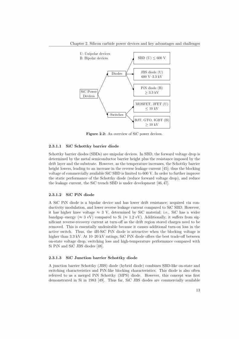
Chapter 2. Silicon carbide power devices and key advantages and challenges
BJT, GTO, IGBT (B)≥ 10 kV
Diodes
Switches
SBD (U) ≤ 600 V
JBS diode (U)600 V–3.3 kV
PiN diode (B)≥ 3.3 kV
MOSFET, JFET (U)≤ 10 kV
SiC PowerDevices
U: Unipolar devicesB: Bipolar devices
Figure 2.2: An overview of SiC power devices.
2.3.1.1 SiC Schottky barrier diode
Schottky barrier diodes (SBDs) are unipolar devices. In SBD, the forward voltage drop isdetermined by the metal semiconductor barrier height plus the resistance imposed by thedrift layer and the substrate. However, as the temperature increases, the Schottky barrierheight lowers, leading to an increase in the reverse leakage current [45]; thus the blockingvoltage of commercially available SiC SBD is limited to 600 V. In order to further improvethe static performance of the Schottky diode (reduce forward voltage drop), and reducethe leakage current, the SiC trench SBD is under development [46,47].
2.3.1.2 SiC PiN diode
A SiC PiN diode is a bipolar device and has lower drift resistance; acquired via con-ductivity modulation, and lower reverse leakage current compared to SiC SBD. However,it has higher knee voltage ≈ 3 V, determined by SiC material; i.e., SiC has a widerbandgap energy (≈ 3 eV) compared to Si (≈ 1.2 eV). Additionally, it suffers from sig-nificant reverse-recovery current at turn-off as the drift region stored charges need to beremoved. This is essentially undesirable because it causes additional turn-on loss in theactive switch. Thus, the 4H-SiC PiN diode is attractive when the blocking voltage ishigher than 3.3 kV. At 10–20 kV ratings, SiC PiN diode offers the best trade-off betweenon-state voltage drop, switching loss and high-temperature performance compared withSi PiN and SiC JBS diodes [48].
2.3.1.3 SiC Junction barrier Schottky diode
A junction barrier Schottky (JBS) diode (hybrid diode) combines SBD-like on-state andswitching characteristics and PiN-like blocking characteristics. This diode is also oftenreferred to as a merged PiN Schottky (MPS) diode. However, this concept was firstdemonstrated in Si in 1983 [49]. Thus far, SiC JBS diodes are commercially available
13

Chapter 2. Silicon carbide power devices and key advantages and challenges
with the maximum voltage and current ratings of 1.7 kV and 100 A per die at roomtemperature and are anticipated to cover the voltage range up to 3.3 kV.
2.3.2 SiC switches
To date, low-voltage (up to 1.7 kV ratings) MOSFETs, JFETs, and BJTs (also calledSJTs, super junction transistors) are the most common commercially available SiCswitches, while high-voltage MOSFETs, JFETs, BJTs, IGBTs, GTOs and ETOs areavailable as engineering samples for research purposes. The following sections outlineonly the transistors’ part as thyristors (GTOs, ETOs) are not in the scope of the thesis.
2.3.2.1 SiC MOSFET
At low-voltage, < 200 V, vertical diffused Si MOSFETs (VDMOSFET) possess low con-duction losses, are capable of switching extremely fast and carrying a high current. Asthe blocking voltage increases, the drift region (epilayer) thickness increases. As a con-sequence, the on-state resistance increases significantly, and, thus, the current carryingcapacity of Si MOSFET has to be reduced to limit the on-state power dissipation [1]. Thisis the reason why VDMOSFETs are not available with high blocking voltage. The emer-gence of the super junction MOSFET (SJ-MOSFET, also called CoolMOS by InfineonTechnologies) technologies enabled Si unipolar transistors to compete up to 900 V.
Alternatively, the remarkably lower drift region resistance in SiC allows the devel-opment of power MOSFETs with higher breakdown voltages and smaller conductionlosses. The first SiC power double diffusion MOSFET 3 (DMOSFET) was introducedin 1996 [50]. Since then different devices have been designed, characterized and stud-ied, aiming to improve their performance. In 2010, the first power SiC DMOSFET wascommercialized by Wolfspeed Inc., which was a vertical device with a planar gate. SiCMOSFETs are the highly-developed devices thus far. As it is both voltage controlledand normally-off, it is the most preferable power switch. Currently, these devices areavailable at different rated voltages from 650 V to 1.7 kV. With VDMOS structure, themaximum available current rating per chip at 25 C is 90 A (25 mΩ, C2M0025120D fromWolfspeed) and with UMOS structure4, it is 118 A (17 mΩ, SCT3017AL from Rohm).Currently, Rohm and Infineon Technologies manufacture SiC MOSFET based on trenchtechnology. SiC MOSFETs up to 15 kV have been reported so far [51–53]. New high-voltage (>3.3 kV) third generation SiC MOSFETs from Wolfspeed are demonstrated withshort-circuit currents up to 13 µs [54]. Primarily, there have been three reliability relatedchallenges associated with SiC MOSFET. The first concerns threshold voltage stabilityof SiC MOSFET, i.e., positive shift with positive gate bias and negative shift with neg-ative gate bias [55]. The second relates to the bipolar degradation of body-diode in SiCMOSFET, i.e., positive shifts in forward voltage of body-diode and on-state loss of SiCMOSFET [56, 57]. The final concerns to the gate-oxide reliability, particularly on thelong term operations, high-temperatures and short circuit conditions [58–60]. All of theseissues have been experimentally verified to be within the safe limit for new-generationSiC MOSFETs [56,61–63].
3Double diffusion MOS (DMOS): the name is taken from the fabrication technique that involves doublediffusion through the same opening: first to create the P region and second for the N source.
4Double trench, gate and source trench MOSFET is called UMOS: the name of the structure comesfrom the U-shapes of the trenches.
14

Chapter 2. Silicon carbide power devices and key advantages and challenges
2.3.2.2 SiC JFET
The first commercialized SiC JFET was a lateral channel JFET (LCJFET) from SiCED(Infineon Technologies). This SiC JFET is a normally-on device. One of the key advan-tages of this device was the easiness for implementation because there were no reliabilityissues with gate-oxide as that with SiC MOSFETs. In fact, there is no surface conductionpath to gate. The second commercially available SiC JFET was the vertical trench JFET(VTJFET), released by SemiSouth Laboratories in 2008. The SiC VTJFET can be pro-duced either as a normally-on (depletion-mode vertical trench JFET, DMVTJFET) or as anormally-off (enhancement-mode vertical trench JFET, EMVTJFET) type. DMVTJFETand EMVTJFET, that is, normally-on and normally-off characteristic is determined byregulating the vertical channel thickness and the doping levels of the structures. Since agate-source voltage has to be applied to stop conduction, the normally-on JFET requiresadditional protection circuitry to prevent short circuiting of DC-bus in case of the poten-tial gate signals failure. This is the reason why the normally-on JFET is not the preferredoption from an application standpoint.
Presently, United Silicon carbide Inc. produces vertical channel JFETs, includingnormally-on, normally-off and cascode types. A cascode configuration comprises of anormally-on SiC JFET and a series-connected low-voltage Si MOSFET. This solutionovercomes the normally-on problem and makes a normally-on JFET behave similarlyto a classical MOSFET. As low-voltage Si MOSFET has a relatively higher thresholdvoltage compared to that of SiC MOSFET, the cascode configuration is regarded as beingsafer from an application viewpoint. Moreover, an off-the-shelf Si MOSFET driver can beadopted for driving cascode JFET. However, the high-temperature potential of SiC JFETis limited by a co-packed Si MOSFET. Currently, these devices are available at differentrated voltages from 650 V to 1.2 kV. SiC JFETs with 6.5 kV have been reported thusfar [64].
2.3.2.3 SiC BJT
Si-based BJT does not favor high-voltage applications for a number of reasons. First,the current gain (β: the ratio of collector current to the base current) was low in SiBJT, which produced high driving losses. For higher current ratings, the gain would bereduced, and thus the losses would increase. Second, minority carrier injection sloweddown Si BJT and caused higher switching losses, which, in turn, generated high dynamicresistance within the device. Third, the BJTs experienced the following reliability issues.(a) Current crowding created high-temperature filaments in the forward-biased mode,which eventually led to device failure. (b) Electrical field stress could be stretched beyondthe drift region due to the voltage and current stresses during the inductive load switching,which could result in reverse-biased breakdown. Accordingly, stringent limits were placedon the Reverse Safe Operation area (RSOA) of the Si BJTs. This indicates that they didnot have short-circuit capability [65].
The implementation of BJTs in SiC, on the other hand, revived this technology be-cause the wider bandgap of SiC enabled higher current gain and thereby minimized thedriving losses and improved the efficiency. SiC BJTs were less susceptible to thermalrunaway, which is attributed to the higher breakdown field of SiC. As a consequence,reliability was greatly increased [65]. The key characterizing parameters that should beaccounted for while choosing SiC BJT are: β, also called common-emitter gain; the spe-
15
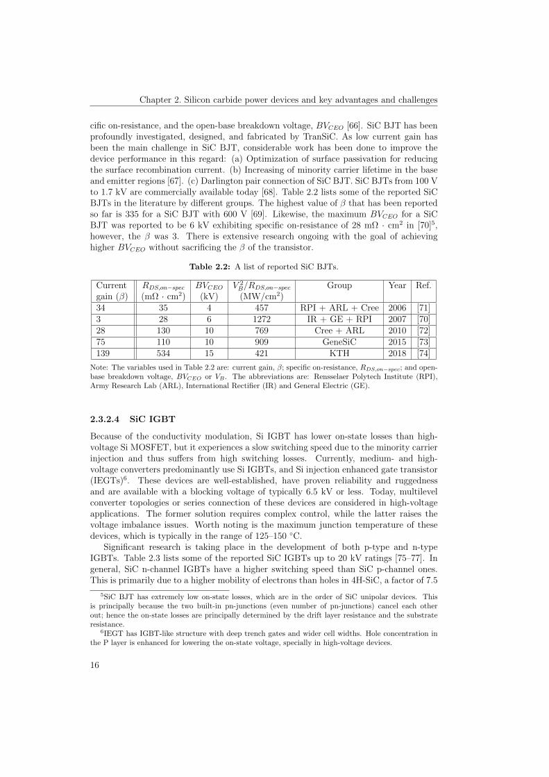
Chapter 2. Silicon carbide power devices and key advantages and challenges
cific on-resistance, and the open-base breakdown voltage, BVCEO [66]. SiC BJT has beenprofoundly investigated, designed, and fabricated by TranSiC. As low current gain hasbeen the main challenge in SiC BJT, considerable work has been done to improve thedevice performance in this regard: (a) Optimization of surface passivation for reducingthe surface recombination current. (b) Increasing of minority carrier lifetime in the baseand emitter regions [67]. (c) Darlington pair connection of SiC BJT. SiC BJTs from 100 Vto 1.7 kV are commercially available today [68]. Table 2.2 lists some of the reported SiCBJTs in the literature by different groups. The highest value of β that has been reportedso far is 335 for a SiC BJT with 600 V [69]. Likewise, the maximum BVCEO for a SiCBJT was reported to be 6 kV exhibiting specific on-resistance of 28 mΩ · cm2 in [70]5,however, the β was 3. There is extensive research ongoing with the goal of achievinghigher BVCEO without sacrificing the β of the transistor.
Table 2.2: A list of reported SiC BJTs.
Current RDS,on−spec BVCEO V 2B/RDS,on−spec Group Year Ref.
gain (β) (mΩ · cm2) (kV) (MW/cm2)34 35 4 457 RPI + ARL + Cree 2006 [71]3 28 6 1272 IR + GE + RPI 2007 [70]28 130 10 769 Cree + ARL 2010 [72]75 110 10 909 GeneSiC 2015 [73]139 534 15 421 KTH 2018 [74]
Note: The variables used in Table 2.2 are: current gain, β; specific on-resistance, RDS,on−spec; and open-base breakdown voltage, BVCEO or VB . The abbreviations are: Rensselaer Polytech Institute (RPI),Army Research Lab (ARL), International Rectifier (IR) and General Electric (GE).
2.3.2.4 SiC IGBT
Because of the conductivity modulation, Si IGBT has lower on-state losses than high-voltage Si MOSFET, but it experiences a slow switching speed due to the minority carrierinjection and thus suffers from high switching losses. Currently, medium- and high-voltage converters predominantly use Si IGBTs, and Si injection enhanced gate transistor(IEGTs)6. These devices are well-established, have proven reliability and ruggednessand are available with a blocking voltage of typically 6.5 kV or less. Today, multilevelconverter topologies or series connection of these devices are considered in high-voltageapplications. The former solution requires complex control, while the latter raises thevoltage imbalance issues. Worth noting is the maximum junction temperature of thesedevices, which is typically in the range of 125–150 C.
Significant research is taking place in the development of both p-type and n-typeIGBTs. Table 2.3 lists some of the reported SiC IGBTs up to 20 kV ratings [75–77]. Ingeneral, SiC n-channel IGBTs have a higher switching speed than SiC p-channel ones.This is primarily due to a higher mobility of electrons than holes in 4H-SiC, a factor of 7.5
5SiC BJT has extremely low on-state losses, which are in the order of SiC unipolar devices. Thisis principally because the two built-in pn-junctions (even number of pn-junctions) cancel each otherout; hence the on-state losses are principally determined by the drift layer resistance and the substrateresistance.
6IEGT has IGBT-like structure with deep trench gates and wider cell widths. Hole concentration inthe P layer is enhanced for lowering the on-state voltage, specially in high-voltage devices.
16

Chapter 2. Silicon carbide power devices and key advantages and challenges
times higher, as listed in Table 2.1. The fabrication of a SiC n-channel IGBT, however,starts on a p-type SiC substrate, which is greatly resistive compared to an n-type one. Asa consequence, the former type is anticipated to exhibit a relatively high specific on-stateresistance compared to the latter one. Other challenges regarding the high-voltage SiCIGBTs are the stability of the gate-oxide layer and the parameter degradation due to thestacking faults.
Table 2.3: A list of reported SiC IGBTs.
SiC IGBT RDS,on−spec BVCEO V 2B/RDS,on−spec Group Year Ref.
types (mΩ · cm2) (kV) (MW/cm2)p-IGBT 18 12 8000 DRAPA + Cree 2008 [78]n-IGBT 22 13 7681 Cree 2009 [79]p-IGBT 130 20 3076 Purdue 2009 [80]
Note: The variables used in Table 2.3 are: specific on-resistance, RDS,on−spec; and open-base breakdownvoltage, BVCEO or VB . The abbreviation is: Defence Advanced Research Projects Agency (DRAPA).
2.4 Comparison of SiC MOSFETs/SiC diodes with
Si MOSFETs/Si diodes
As this thesis aims for an evaluation of the latest generations of SiC MOSFETs and SiCdiodes, the focus here onwards will primarily be on these devices.
2.4.1 Structures of MOSFET
Before exploring the details of state-of-the-art MOSFET devices, it is vital to brieflyconsider their structures and the purposes behind them. Overall, there are three majorstructures of MOSFET: vertical diffused MOS (VDMOS) structure, UMOS structure(also called trench-MOS structure), and super junction (SJ) structure. The total on-resistance, RDS,on, consists of the sum of the channel resistance, the JFET resistance andthe substrate resistance. In low-voltage devices, the channel-resistance is the predominant,while in high-voltage devices, the drift resistance is the dominant resistive component [56].As the blocking voltage of Si MOSFETs exceeds 200 V, RDS,on increases. To cope withthis challenge, other structures, such as the UMOS structure, where the gate electrodeis buried in a trench and the SJ structure, where a charge compensation principle isused, have been introduced. The former structure provides the potential to reduce thechannel resistance and eliminate the JFET resistance, which makes the trench MOSFETvery attractive for the lower voltage ratings [56]. The latter structure minimizes the driftlayer resistance. Fig. 2.3 shows the structures of SiC MOSFET with planar versus trenchtechnology [46,47].
2.4.2 Comparison of SiC MOSFETs with Si MOSFETs
Table 2.4 compares the most significant parameters, in particular, the maximum break-down voltage (VDS), current (ID), on-state resistance (RDS,on), internal gate resistance(Rg,int), total gate charge (Qg), gate-drain charge (Qgd), input capacitance (Ciss), output
17
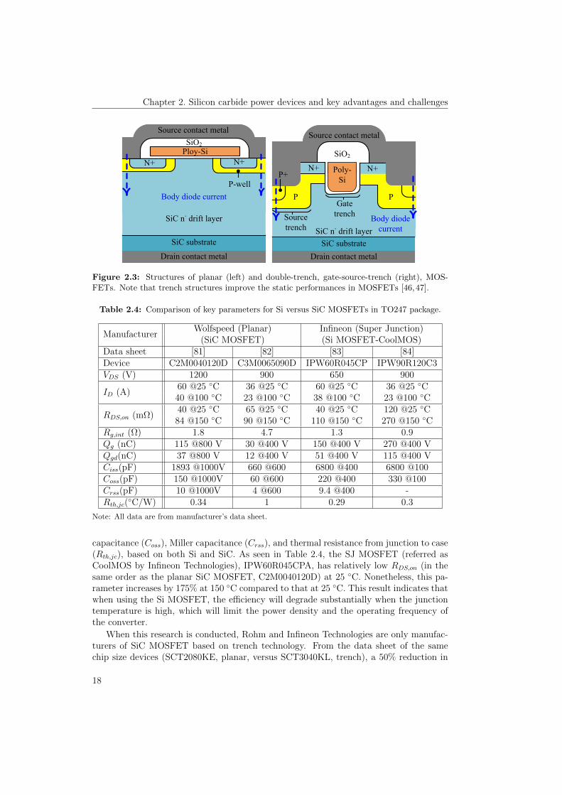
Chapter 2. Silicon carbide power devices and key advantages and challenges
Drain contact metal
SiC substrate
SiC n- drift layer
N+
P
N+P+
Poly-Si
SiO2
Source contact metal
P
Source trench
Gate trench
Drain contact metal
SiC substrate
SiC n- drift layer
Ploy-SiSiO2
Source contact metal
N+ N+
Body diode current
Body diode current
P-well
Figure 2.3: Structures of planar (left) and double-trench, gate-source-trench (right), MOS-FETs. Note that trench structures improve the static performances in MOSFETs [46,47].
Table 2.4: Comparison of key parameters for Si versus SiC MOSFETs in TO247 package.
ManufacturerWolfspeed (Planar) Infineon (Super Junction)
(SiC MOSFET) (Si MOSFET-CoolMOS)Data sheet [81] [82] [83] [84]Device C2M0040120D C3M0065090D IPW60R045CP IPW90R120C3VDS (V) 1200 900 650 900
ID (A)60 @25 C 36 @25 C 60 @25 C 36 @25 C40 @100 C 23 @100 C 38 @100 C 23 @100 C
RDS,on (mΩ)40 @25 C 65 @25 C 40 @25 C 120 @25 C84 @150 C 90 @150 C 110 @150 C 270 @150 C
Rg,int (Ω) 1.8 4.7 1.3 0.9Qg (nC) 115 @800 V 30 @400 V 150 @400 V 270 @400 VQgd(nC) 37 @800 V 12 @400 V 51 @400 V 115 @400 VCiss(pF) 1893 @1000V 660 @600 6800 @400 6800 @100Coss(pF) 150 @1000V 60 @600 220 @400 330 @100Crss(pF) 10 @1000V 4 @600 9.4 @400 -Rth,jc(
C/W) 0.34 1 0.29 0.3
Note: All data are from manufacturer’s data sheet.
capacitance (Coss), Miller capacitance (Crss), and thermal resistance from junction to case(Rth,jc), based on both Si and SiC. As seen in Table 2.4, the SJ MOSFET (referred asCoolMOS by Infineon Technologies), IPW60R045CPA, has relatively low RDS,on (in thesame order as the planar SiC MOSFET, C2M0040120D) at 25 C. Nonetheless, this pa-rameter increases by 175% at 150 C compared to that at 25 C. This result indicates thatwhen using the Si MOSFET, the efficiency will degrade substantially when the junctiontemperature is high, which will limit the power density and the operating frequency ofthe converter.
When this research is conducted, Rohm and Infineon Technologies are only manufac-turers of SiC MOSFET based on trench technology. From the data sheet of the samechip size devices (SCT2080KE, planar, versus SCT3040KL, trench), a 50% reduction in
18

Chapter 2. Silicon carbide power devices and key advantages and challenges
RDS,on and a 35% reduction in Ciss are achieved by switching the technology from theplanar to the trench type [85]. As per RDS,on, SCT3017AL and SCT3022KL with trenchstructures are the most interesting DUT candidates today. Note that the Rg,int of theMOSFET depends on the sheet resistance of the gate electrode material and the chip size.Specifically, Rg,int is inversely proportional to the chip size [85]. The chip size of the SiCMOSFET is smaller than that of the Si MOSFET, leading to a larger Rg,int and a smallergate capacitance in SiC, provided that the ratings are the same, which can be explicitlyseen from the comparison shown in Table 2.4. Note that a higher value of Rg,int limitsthe switching speed of the SiC MOSFET. It should be mentioned that a trade-off existsbetween the conduction and switching losses for a device. A device with a larger die size(A) exhibits reduced conduction loss (RDS,on ∼ 1/A), but leads to increased switchingloss (Ciss ∼ A).
2.4.3 Structures of diode
There are basically two types of diodes: the PiN diode and the Schottky diode. Thisthesis centers on the Schottky type only. Fig. 2.4 shows the two major structures of theSchottky diode, namely, planar and trench.
Schottky metal
SiC substrate
Metal
N-SiC (drift layer)
N-SiC (drift layer)
Schottky metal
P-SiC
SiC substrate
Metal
Figure 2.4: Structures of planar (left) and trench (right) SBD.
2.4.4 Comparison of SiC diodes with Si diodes
Table 2.5 documents the key electrical parameters, including the maximum breakdownvoltage (VDS), forward current (IF ), forward voltage drop (VF ), reverse-recovery chargeof a Si diode (Qrr), and capacitive charge of a SiC diode (Qc), for state-of-the-art diodes,based on both Si and SiC with two different voltage ratings: 650 V and 1200 V. In par-ticular, VF and Qrr or Qc are desired to be the lowest to achieve the highest efficiency.Schottky barrier diodes exhibit both of these features compared to other diode technolo-gies, for instance, the fast recovery epitaxial diode (FRED) [88, 89]. Nevertheless, thenarrow bandgap of Si limits its use to a maximum voltage of approximately 200 V, i.e.,Si SBDs that operate above 200 V have higher VF and Qrr.
Before the advent of SiC Schottky diodes, bipolar pn-junction FREDs were the onlysolutions for applications requiring diodes with blocking voltages in excess of 200 V. It is
19

Chapter 2. Silicon carbide power devices and key advantages and challenges
Table 2.5: Comparison of key parameters for Si- versus SiC Schottky diodes in TO247 package.
ManufacturerROHM (Planar) Vishay (FRED PT) IXYS (FRED)(SiC JBS diode) (Si diode) (Si diode)
Data sheet [86] [87] [88] [89]Device SCS220AE2 SCS220KE2 VS-EPH3007L-N3 DSEI30-12AVDS (V) 650 1200 650 1200IF (A) 20 @135 C 20 @145 C 30 @100 C 30 @100 C
VF (V)1.35 @25 C 1.4 @25 C 1.8 @25 C 2.55 @25 C1.55 @150 C 1.8 @125 C 1.4 @150 C 2.2 @150 C
Qrr/ Qc (nC)30 68 1350 3000
@400 V @800 V @400 V, 125 C @540 V, 100 CRth,jc (C/W) 0.8 0.45 0.7 0.25
Note: All data are from manufacturer’s data sheet.
worth mentioning that SiC SBDs or SiC JBS diodes maintain a constant recovery chargeregardless of temperature and forward current, but this charge significantly increases inthe similar rating Si FRED [90]. There are two main explanations for this behavior. First,SiC SBDs and SiC JBS diodes are majority carrier devices, and there is no minority carrierinjection as in the Si FRED. Second, SiC has a significantly smaller chip size comparedto Si, and, consequently, little or no charge storage mechanism exists in SiC. As seenin Table 2.5, the Qrr of Si diodes also contains information about the temperature, butthis information is not provided for SiC diodes because the Qc of SiC is temperatureindependent. Another interesting observation from Table 2.5 is that the VF in Si FREDhas a negative temperate coefficient, whereas the opposite is true in SiC JBS diodes. InSi FREDs, as the temperature rises, the Fermi level moves, and, then, the barrier heightlowers, leading to a decrease in VF . In contrast, in SiC JBS diodes, as the temperatureincreases, the lattice vibration increases and the mobility decreases, resulting in higherresistance [45].
2.5 Packaging
This section provides a brief overview of the commercially available packages of SiC de-vices. Low-power discrete SiC devices are available in different packages, such as TO247-3,TO247-4, TO263-7. All of these devices showed outstanding static and dynamic perfor-mance compared to their Si contenders. It is obvious that the chip size determines thecurrent rating of a device; however, the low yield of SiC wafer and thermal mechanicalstress restrict the device area. As a consequence the current capability of a single chip islimited. Therefore, for high current power modules, multiple chips are paralleled to forma single switch. Several features, including electrical connections, thermal conductionto heat sink, electrical insulation, and mechanical support are contained in a standardpower module package. This consists of a chip, wire bond, solder, Cu, Ceramic, Cu,(Cu-Ceramic-Cu is often called DBC, direct bonded copper substrate) solder, baseplate,thermal grease and heat sink or cold plate arranged from top to bottom. Al2O3, AlN,Si3N4 are the most common ceramic materials. DBC substrate conducts the heat gener-ated by the chip to the cooling system and provides an insulation layer between the chip
20

Chapter 2. Silicon carbide power devices and key advantages and challenges
Table 2.6: Commercially available SiC modules and their package inductance.
Manufacturer Lmodule (nH) RemarksWolfspeed-45 mm 30 Standard moduleWolfspeed-62 mm 15 Standard moduleWolfspeed-62 mm 5 High performanceSanrex 15 Solder bondingRohm type C 25 Standard moduleVincotech 7 Additional low-inductive current path
and the baseplate. Wire bond functions as the electrical connection between the top sideof one chip and the other chips [91].
Table 2.6 lists the commercially available power module packages with their internalinductances. They are packaged in similar standard module packages as those used for Sidevices. Wire bond interconnection is used in all of them except in Sanrex module, wherea solder bond technique is employed. At high power level, the dynamic performance ofSiC devices is limited by the parasitics in the module housing, as well as in the externalbusbar and gate drive circuitry. This is primarily a result of the parasitics becoming alivewith higher dv/dt and di/dt.
To bridge the gap between SiC devices and their applications, manufacturers havestarted to look into improved and advanced packaging techniques. One example is themodule from Vincotech, which uses a separate RC (resistance and capacitance) loop closeto the power module, apart from the main DC-link capacitor. The former is active duringswitching when di/dt is high. The capacitor is realized via PCB or foil [26]. Anotherexample is the Semikron SKiN technology introduced in 2011 for Si IGBTs, where allsoldering and bonding connections of standard power module designs are replaced bysilver diffusion sintering joints; i.e., the thin flexible layer takes over the function of bondwires. This resulted in a significant reduction in commutation inductance (3.2 nH) [25].
2.6 Critical thinking or challenges
Critical thinking is indispensable whenever new devices come onto the market. Here,some of the key challenges associated in unlocking the full-potential offered by SiC arediscussed.
First, SiC allows fast switching speed enabling extremely high (> 200 kHz) switchingfrequencies in SMPS applications (in the kW range). However, its dynamic perfor-mance is hindered by the parasitics in the transistor casing and in the externalbusbar and gate drive circuitry. Furthermore, various phenomena like parasitic ringingsand electromagnetic interference (EMI) are augmented as dv/dt and di/dt increase. Thus,significant research efforts are ongoing regarding low-inductive packaging and busbar de-sign as reported in [25–28,92–97].
Second, although the physics of SiC permit maximum junction temperatures wellabove 200 C, constraints are placed on other parts of the system, such as high-temperature packaging technology. Numerous research projects have been conductedin this direction and some interesting examples of these can be found in [95,96,98].
Third, SiC is an emerging technology, special gate drivers that are fast enough
21

Chapter 2. Silicon carbide power devices and key advantages and challenges
to operate gates in the nanoseconds range (high charge and discharge pulse current)are required for switching the devices to their fast-switching potential. Further, uniquegate drive voltages are needed as per the device technology. For instance, manufacturersrecommend +20 V/-5 V gate voltages for most of the SiC MOSFETs [81,99], while third-generation SiC MOSFET from Wolfspeed requires +15 V/-4 V [82]. Similarly, InfineonTechnologies recommend selecting lower limit of turn-off voltage depending on the turn-onvoltage in their trench MOSFETs [100]. This aims in keeping the drift in gate-thresholdvoltage within the acceptable limits. There has been a wealth of discussion and researchin the direction of gate driver design suitable for a high-temperature and high-frequencyenvironment, some of which are reported in [101–106].
Finally, SiC is not only a part in a converter, the neighbouring components should alsobe able to sustain the same environment without deteriorating the mechanical, electrical,thermal and electromagnetic properties. Currently, the availability of such ancillarycomponents, such as capacitors and inductors, capable of living in the same environmentas SiC, is a serious impediment for harvesting the benefits offered by SiC. In addition,the insulation requirement when a single-device blocking voltage is in the tens of kilovoltsshould also be borne in mind. Therefore, advancements in semiconductors should go handin hand with the complementing bodies. To overcome some of these challenges, a similarconcept as used in Si technology, referred to as an intelligent power module (IPM), wherethe drive and protection circuitry are integrated along with a semiconductor [107], is beingleveraged in SiC. SiC-based IPMs [108, 109], optimized gate drives for the commercialSiC modules [110, 111] are already released. Other efforts in this direction are reportedin [101,112–114].
Thus, to develop converters with unprecedented efficiency and power density, the nextlandmark would be the integration of passives, WBG semiconductors, gate driver, control,protection, communication and thermal management to the extent it makes meaning[112,115,116]. Texas instruments and Vicor have lunched several such products [115,116],for instance, 10 kW, three-phase AC to 48 V converter power-on-package solution wasintroduced by Vicor in 2018 [117].
2.7 Summary
This chapter started with a comparison of material properties of the most interestingsemiconductors. With the special attention directed to the SiC devices, the chapterdiscussed various SiC devices that are commercially available and in research along withthe benefits and challenges associated with each of them. Next, particular focus was paidto SiC MOSFETs and SiC diodes, together with the detailed comparison of state-of-the-art SiC versus Si devices and the packages they come with. Finally, the challenges inadopting this technology were addressed.
22

Chapter 3
Prerequisites for accurate assessmentof switching loss by electrical method
The information presented in this chapter is based on publications J2 and C11, the mainaim of which is to answer the following research questions.
Q 1. What are the prerequisites for accurate assessment of switching losses of SiC devices?
Q 2. Can the electrical loss measurement via a widely accepted double-pulse test (DPT)methodology with inductive clamped load be used for estimating the losses that occurin a resonant (sine wave current) inverter?
3.1 Introduction
The results of this work are primarily based on laboratory experiments. This chapter isdivided into two parts. The first part concerns the provisos for evaluating the switch-ing performance of SiC devices, which covers appropriate probes and oscilloscope foraccurately tracking the fast switching transients of these devices. Following this, thelow-inductive connection techniques and characteristics of load which are imperative forcapturing the true switching waveforms of device under test (DUT) are exemplified. Fi-nally, the importance of accuracy in post processing of the measured data is included.
The second part, on the other hand, is related to the significance of realistic topologyfor an accurate assessment of switching losses, where a widely accepted DPT methodologyis employed. For representing the hard-switched application, a clamped inductive loadis used, while for portraying the resonant-switched application, split DC-link capacitorswith series connection of inductance and capacitance (LC) as load are used. Comparisonof the turn-off loss measured between these two configurations revealed that the resonant(sine wave current) switching technique achieved considerably lower losses compared tothe hard (square wave current) switching operation. Thus, this chapter primarily rec-ommends using an appropriate circuit topology for the correct assessment of switchingloss. Apart from reducing switching losses, the resonant inverter topology also entailedin mitigating the oscillations, which can subsequently alleviate electromagnetic interfer-ence (EMI). Based on this outcome, the author suggests adopting the sine wave switchingtechnique whenever possible (as per the application).
23

Chapter 3. Prerequisites for accurate assessment of switching loss by electrical method
3.2 Prerequisites for accurate measurement of high-
speed switching signals
3.2.1 Bandwidth of measuring probes and oscilloscope
In order to capture the fast rising and falling current and voltage signals of switchingdevices, the probes and oscilloscope should have adequate bandwidth (BW) or rise time(trise) and fall time (tfall). If not, the harmonics which are above the cut-off frequencyof probe will be filtered out and the measured di/dt and dv/dt will be lower than thereal slopes leading to inaccurate results. In [118], it is recommended to have five timesgreater BW of the probe and oscilloscope compared to the frequency of the waveformbeing measured. Moreover, it is also suggested that, for accurately tracking trise and tfallof the waveform, the BW of equipment should satisfy the relation given by (3.1). Asan illustration, Fig. 3.1 is presented where the trise of drain-source voltage (Vds) is 20 nsfor an external gate resistance (Rg,ext) of 0 Ω. Based on (3.1), BW is computed to be87.5 MHz, indicating that the oscilloscope and probes with higher BW than 87.5 MHzare of sufficient quality to track the transient waveforms of that particular device. Inaddition, frequency of oscillations (fosc) is measured to be 30 MHz, therefore, 150 MHz ofBW is enough for tracking these oscillations. It is worth mentioning that the oscilloscopeis calibrated in order to adjust its parameters according to surrounding environmentalconditions, such as temperature, pressure, and humidity, each time the measurement istaken.
BW = 5 · 0.35
trise [ns]= 5 · 0.35
20= 87.5 MHz (3.1)
-1000 -500 0 500 1000time [ns]
-20
0
20
40
60
80
100
120
Figure 3.1: For Rg,ext = 0 Ω, the trise and tfall are in the range of 20 ns and the ringingfrequency (fosc) is 30 MHz, thus the probes and oscilloscope bandwidth of ≥ 150 MHz areadequate for tracking these switching transients. The legends used in Fig. 3.1 are: Vds, drain-source voltage; Ids, drain-source current; and Vgs, gate-source voltage.
24

Chapter 3. Prerequisites for accurate assessment of switching loss by electrical method
3.2.1.1 Voltage measurement
High BW and sufficient dynamic range are two important requirements of voltage probes.Table 3.1 summarizes the probes considered in this work. Passive probes are used formeasuring low-side Vgs and Vds in the phase-leg configuration. Differential probes areused for high-side Vgs and Vds measurements because they also have galvanic isolation,while the passive probes do not. Moreover, common mode (CM) input voltage range andCM rejection ratio are also critical for high-side voltage measurements. All of these probeshave their own propagation delays and have to be individually dealt with while computingthe switching losses. Furthermore, the voltage probes are compensated to adjust theircapacitances according to the input capacitance of the oscilloscope channel.
Table 3.1: Data sheet readings of voltage measurement probes used in the thesis.
Types Models Max. voltage Bandwidth Rise time1 DelayDifferential probe THDPO200 ± 1500 V 200 MHz 8.75 ns 14 ns
Passive probeP5100A 2500 V 500 MHz 3.50 ns 6.1 ns
TPP1000 750 V 1000 MHz 1.75 ns 5.67 ns
1Rise-time is calculated based on (3.1) with five times margin (i.e., 5 × 0.35/Bandwidth).
3.2.1.2 Current measurement
Current measurement techniques, such as coaxial shunt, split-core current probe, andRogowski coil are adopted in this thesis, the specifications of which are summarized inTable 3.2. All of these probes have their own pros and cons. Although the Rogowski coilfeatures galvanic isolation, and can be easily connected to the device, it has limitationsregarding the BW and DC-component measurement. Therefore, it is not sufficientlyaccurate for measuring the high-speed switching current. The coaxial shunt, on the otherhand, has high BW and high accuracy, but does not feature galvanic isolation. Moreover,it cannot be used for measuring current in continuous operation.
Table 3.2: Current measurement techniques and their specifications as per data sheet.
Types Models Current type Bandwidth Rise time1
Coaxial shuntSDN - 25, 250 mΩ dc/ac 1000 MHz 1.75 ns
SSDN - 414 - 01, 10 mΩ dc/ac 400 MHz 4.37 nsSplit-core TCP0030A dc/ac 120 MHz 14.58 nsRogowski coil CWT6B ac 30 MHz 58.3 ns
1Rise-time is calculated based on (3.1) with five times margin (i.e., 5 × 0.35/Bandwidth).
3.2.2 Low-inductive measurement connections
Ground-lead inductance is another factor impacting the measurement accuracy of switch-ing waveforms, as discussed in [118,119], because the typical ground-lead associated withthe voltage probe has an inductance and forms a series-resonant network with the inputcapacitance of the probe. Therefore, a PCB probe-tip adapter is employed in order toreduce the ground-lead inductance, as shown in Fig. 3.2 (a) and (b).
25

Chapter 3. Prerequisites for accurate assessment of switching loss by electrical method
Current shunt
1 GHz
Probe-tip adapters
Voltage probes
500 MHz -1 GHz
Current probe, 120 MHz
Ferrite core transformer
(a) Probe-tip adapters connections.
Case 2
Case 1
(b) Ground-lead of a voltage probe.
Figure 3.2: (a) Laboratory setup showing the arrangement for low-inductive connections forcurrent and voltage measurements of the device under test. The current is measured by ahigh-bandwidth, low-inductive current shunt, and the voltage is measured by a high-bandwidthsingle-ended probe with probe-tip adapter as displayed. (b) Illustration of a typical ground-lead of a voltage probe (Case 1) versus probe-tip adapter connection (Case 2). Load current ismeasured by a dc/ac current probe out of a 40-turn ferrite core transformer.
3.2.3 Load inductor characteristics
Two single-layer winding air core inductors are connected in series as an inductive load.The air core avoids saturation, single-layer winding provides small stray capacitance (CL),and the series connection further reduces CL, and subsequently the true switching wave-forms of the DUT are reflected. The equivalent CL of the load inductor is measured byan impedance analyzer, E4990, and is found to be 1 pF.
3.2.4 Post processing of measured data
3.2.4.1 De-skewing of voltage probes
Generally, the data sheet of the voltage probe provides information about probe delay,which is 14 ns for the selected probe. In order to analyze the influence of the probe delayon the accuracy of measurement, the voltage waveform is de-skewed, i.e., subtracting theprobe delay from the originally measured voltage waveform, as shown in Fig. 3.3 (a).The originally measured voltage waveform is in dotted blue and the one with de-skewedis indicated by solid blue. As the current waveform is measured by a shunt resistor,there is no need to de-skew the current waveform. Thereafter, the current and voltagewaveforms are multiplied to obtain the power loss indicated by the dotted red line forthe original and the solid red line for the de-skewed. Then, the switching energy loss iscalculated for the case with and without probe de-skew. With the former, the specificenergy loss (Eoff−spec−elec) is computed to be 9.94 µJ/A, whereas the same with the latteris calculated to be 5.18 µJ/A; lower by a factor of 1.91.
26

Chapter 3. Prerequisites for accurate assessment of switching loss by electrical method
0 200 400 600 800time [ns]
-20
0
20
40
60
80
100
120
(a) Turn-off event with and without probe de-skew.
0 200 400 600 800time [ns]
-20
0
20
40
60
80
100
120
(b) Turn-off event with different integration time.
Figure 3.3: Turn-off transients during hard-switching together with the power waveforms.Fig. (a) illustrates the influence of probe delay. With 14 ns of voltage probe delay with respectto current measured by shunt, there is a significant difference in the computed energy loss.Fig. (b) exposes the influence of integration limits on the power curve. Given that there areoscillations, the choice of the end of the integration time is not clear. tA denotes the start of theintegration time, while tB and tC are two options to select the end of the integration time.
3.2.4.2 Choosing the time interval for power integration
The selection of an appropriate time interval is crucial for integrating the measured powerin order to extract the correct switching energy loss, an example of which is illustratedin Fig. 3.3 (b). Both current and voltage waveforms exhibit oscillations at the end ofeach switching transient and so do the power curves possessed. There are two possibleintegration time limits. The first is the initial zero crossing of power curve, indicated bytC , the second is tB, where the low and high-frequency oscillations have decayed. Whileintegrating the power waveform from tA to tB, Eoff−spec−elec is computed to be 9.94 µJ/A,whereas when integrating the power waveform from tA to tC , the same is computed tobe 8.82 µJ/A; lower by 11.26%. In this work, the former integration limit where all theoscillations are decayed is considered.
3.3 Importance of realistic circuits for loss evaluation
In this section, the significance of using an appropriate inverter topology for the correctassessment of the switching loss is investigated. Two different topologies studied involvea half-bridge inductive clamped load without split DC-link capacitors, which has a squarewave output current; and a half-bridge series-resonant inverter with split DC-link capaci-tors and an LC load, which has a sine wave output current. For realizing a low switchingloop stray inductance, the DC-link is made with a planar busbar, except for the termina-tion parts needed to facilitate the module connection. A current viewing resistor (CVR),also called a shunt resistor, SSDN-414-01 (400 MHz, 10 mΩ) from T & M research, isused for measuring the drain current. The CVR is mounted directly on one of the screwterminals of the SiC MOSFET module, as illustrated in Fig. 3.4.
27
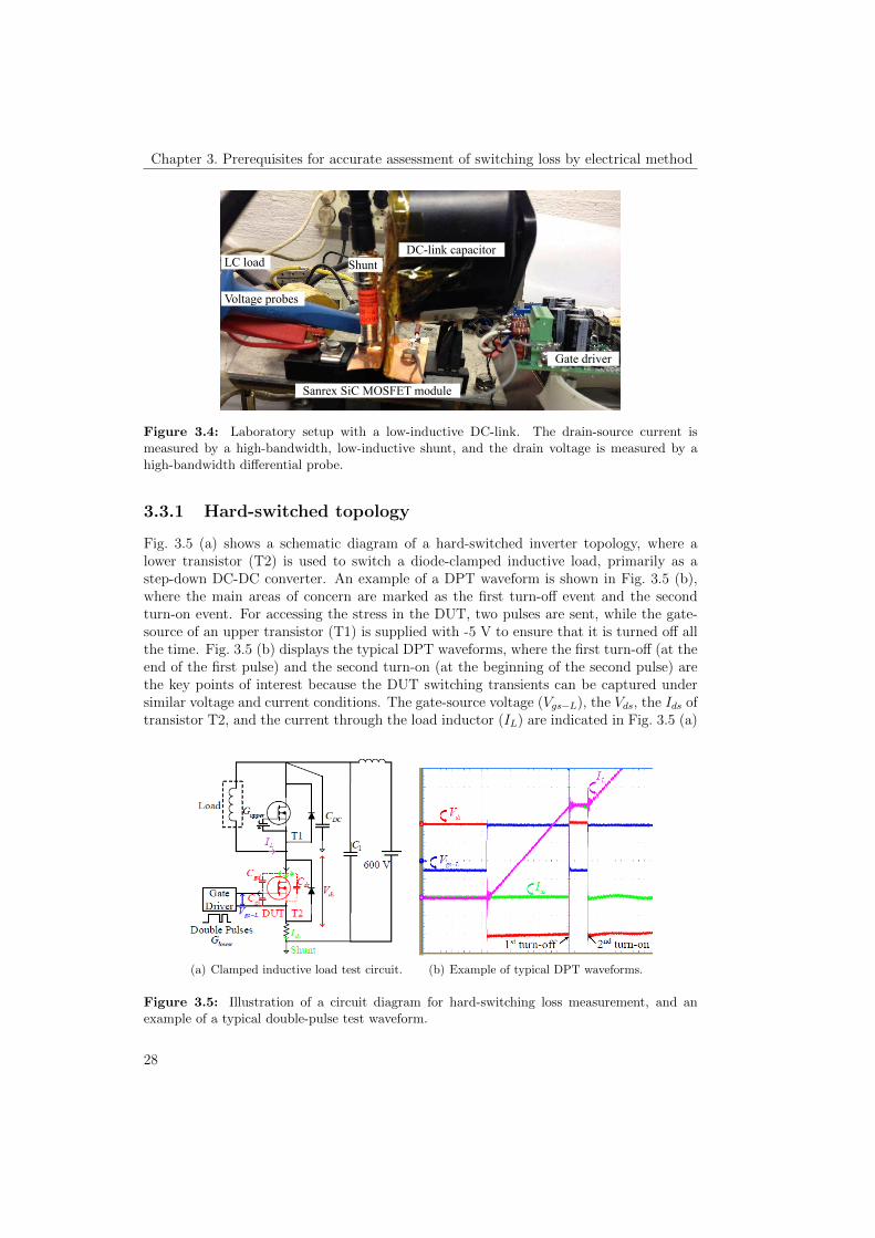
Chapter 3. Prerequisites for accurate assessment of switching loss by electrical method
DC-link capacitor
Gate driver
Shunt
Sanrex SiC MOSFET module
Voltage probes
LC load
Figure 3.4: Laboratory setup with a low-inductive DC-link. The drain-source current ismeasured by a high-bandwidth, low-inductive shunt, and the drain voltage is measured by ahigh-bandwidth differential probe.
3.3.1 Hard-switched topology
Fig. 3.5 (a) shows a schematic diagram of a hard-switched inverter topology, where alower transistor (T2) is used to switch a diode-clamped inductive load, primarily as astep-down DC-DC converter. An example of a DPT waveform is shown in Fig. 3.5 (b),where the main areas of concern are marked as the first turn-off event and the secondturn-on event. For accessing the stress in the DUT, two pulses are sent, while the gate-source of an upper transistor (T1) is supplied with -5 V to ensure that it is turned off allthe time. Fig. 3.5 (b) displays the typical DPT waveforms, where the first turn-off (at theend of the first pulse) and the second turn-on (at the beginning of the second pulse) arethe key points of interest because the DUT switching transients can be captured undersimilar voltage and current conditions. The gate-source voltage (Vgs−L), the Vds, the Ids oftransistor T2, and the current through the load inductor (IL) are indicated in Fig. 3.5 (a)
(a) Clamped inductive load test circuit. (b) Example of typical DPT waveforms.
Figure 3.5: Illustration of a circuit diagram for hard-switching loss measurement, and anexample of a typical double-pulse test waveform.
28
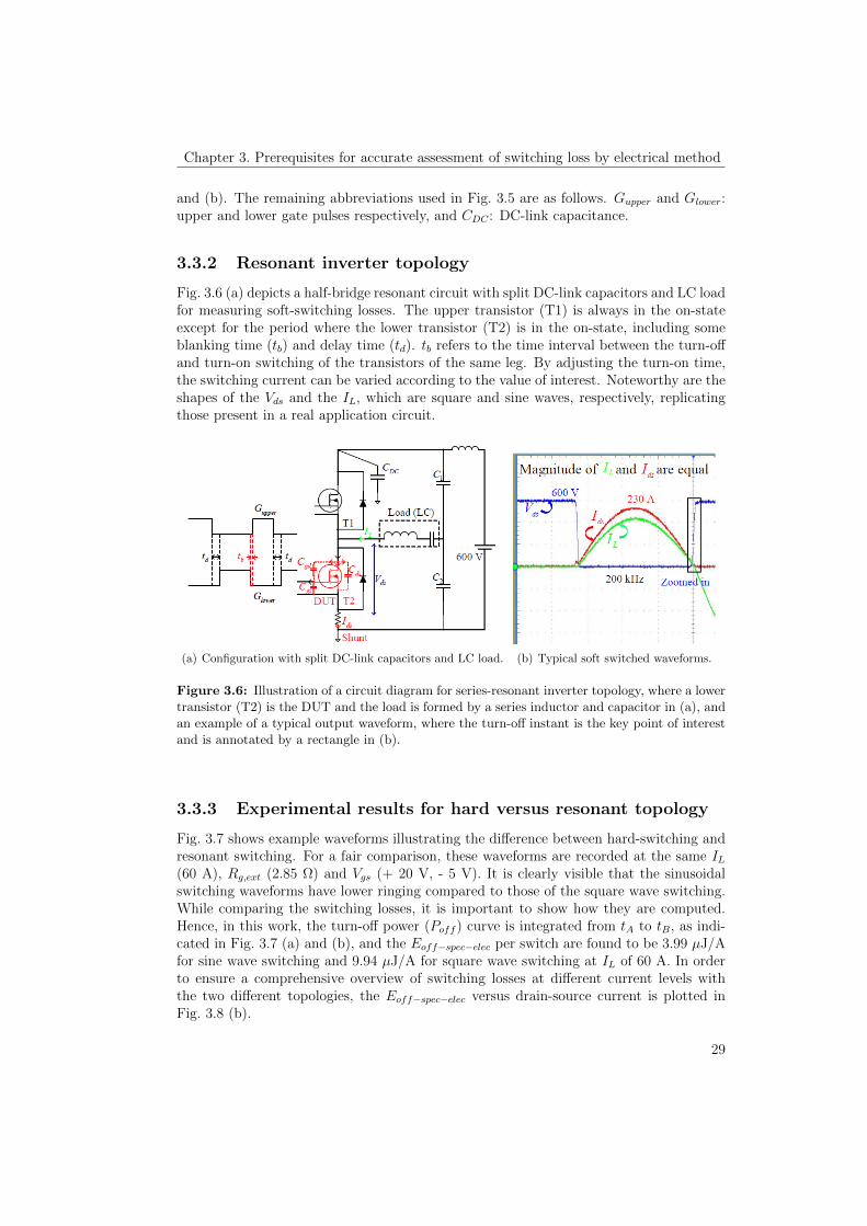
Chapter 3. Prerequisites for accurate assessment of switching loss by electrical method
and (b). The remaining abbreviations used in Fig. 3.5 are as follows. Gupper and Glower:upper and lower gate pulses respectively, and CDC : DC-link capacitance.
3.3.2 Resonant inverter topology
Fig. 3.6 (a) depicts a half-bridge resonant circuit with split DC-link capacitors and LC loadfor measuring soft-switching losses. The upper transistor (T1) is always in the on-stateexcept for the period where the lower transistor (T2) is in the on-state, including someblanking time (tb) and delay time (td). tb refers to the time interval between the turn-offand turn-on switching of the transistors of the same leg. By adjusting the turn-on time,the switching current can be varied according to the value of interest. Noteworthy are theshapes of the Vds and the IL, which are square and sine waves, respectively, replicatingthose present in a real application circuit.
(a) Configuration with split DC-link capacitors and LC load. (b) Typical soft switched waveforms.
Figure 3.6: Illustration of a circuit diagram for series-resonant inverter topology, where a lowertransistor (T2) is the DUT and the load is formed by a series inductor and capacitor in (a), andan example of a typical output waveform, where the turn-off instant is the key point of interestand is annotated by a rectangle in (b).
3.3.3 Experimental results for hard versus resonant topology
Fig. 3.7 shows example waveforms illustrating the difference between hard-switching andresonant switching. For a fair comparison, these waveforms are recorded at the same IL(60 A), Rg,ext (2.85 Ω) and Vgs (+ 20 V, - 5 V). It is clearly visible that the sinusoidalswitching waveforms have lower ringing compared to those of the square wave switching.While comparing the switching losses, it is important to show how they are computed.Hence, in this work, the turn-off power (Poff ) curve is integrated from tA to tB, as indi-cated in Fig. 3.7 (a) and (b), and the Eoff−spec−elec per switch are found to be 3.99 µJ/Afor sine wave switching and 9.94 µJ/A for square wave switching at IL of 60 A. In orderto ensure a comprehensive overview of switching losses at different current levels withthe two different topologies, the Eoff−spec−elec versus drain-source current is plotted inFig. 3.8 (b).
29

Chapter 3. Prerequisites for accurate assessment of switching loss by electrical method
0 200 400 600 800time [ns]
-20
0
20
40
60
80
100
120
(a) Switching event with hard-switched topology.
0 200 400 600 800time [ns]
-20
0
20
40
60
80
100
120
(x, y) = (90, 60)
(b) Switching event with resonant topology.
Figure 3.7: (a) Illustration of turn-off transients under hard versus resonant topology at thesame load current. The former exhibits oscillations, while oscillations are absent in the latter.Specifically, the turn-off energy loss is 2.5 times lower for resonant topology than that of thehard-switched inverter, showing the ample benefit of the latter topology.
0 0.5 1 1.5 2 2.5time [ s]
0
30
60
90
120
150
180
210
240 230
210
180
150
120
90
60
30
(a) Definition of turn-off current.
0 30 60 90 120 150 1800
2
4
6
8
10
12
14
16
4.5
1.2
(b) Comparison of switching loss.
Figure 3.8: (a) Illustration of the turn-off current in the resonant switching case. The peakvalue of the load current is set at 230 A, and the turn-off instants are varied. (b) Comparison ofthe switching loss between the hard (square wave current) and soft/resonant (sine wave current)switching. Switching with square wave current leads to higher turn-off losses, a factor of 1.2(150 A) to 4.5 (30 A) depending on the load current, compared to that with sine wave current.
It is worth mentioning that, in either of the topologies, the required turn-off currentlevel is acquired by adjusting the on-time and the DC-link voltage. To be more preciseregarding the resonant switching, the peak value of the load current is fixed at 230 A,and, thereafter, the turn-off instants are varied (by adjusting the on-time), as defined inFig. 3.8 (a). Aside from this, the switching frequency is set to 200 kHz according to theapplication requirements. Depending on Ids, Eoff−spec−elec varies from 2 to 10.8 µJ/A
30

Chapter 3. Prerequisites for accurate assessment of switching loss by electrical method
with the resonant topology and from 9 to 12.8 µJ/A with the hard-switched topology.Thus, using the hard-switching loss for designing thermal management and estimating
the power rating of the resonant inverter leads to a significant error, as the turn-offswitching in the latter occurs at the minimum possible current (lower current regions).The difference in losses between the two topologies is more pronounced towards the lowercurrents, primarily for two reasons. First, at lower current, there is lower dv/dt, whichcauses the output capacitance of the MOSFET to work more effectively as a turn-offsnubber compared to a higher current. Second, the MOSFET channel is closed to thecurrent earlier in the turn-off process with lower dv/dt.
3.4 Summary
This chapter centred on accessing the true switching waveforms as in a real-world invertercircuit, and can be summarized as follows:
1. First a half-bridge configuration, a basic cell or a part of many topologies is consideredfor study, so that all the parasitics are involved during the switching events. Key issuesimpacting the high-speed measurements are discussed, and the measures for accuratelytracking the fast switching transients and evaluating the switching losses by electricalmethod, such as selection of voltage probes, current probes, and oscilloscope withadequate BW; probe-tip adapter for minimizing connection inductances; adjustmentsof probe de-skew and possible post-processing errors are highlighted.
2. Keeping the gate driver stray inductance, resistance, voltage and location the same inhard versus resonant inverter topologies, the turn-off switching losses are compared.Measured results revealed that the resonant (sine wave current) switching techniquecauses remarkably lower loss compared to the hard (square wave current) switchingoperation, a factor of 2.5 times lower at 60 A. Thus, the author has two key recom-mendations.
i. First, adopt resonant switching whenever feasible (as per the application) becausethis minimizes the switching losses and oscillations.
ii. Second, consider an appropriate circuit topology for the correct assessment ofswitching loss, especially for a resonant inverter, where the turn-off is aimedtowards the lower current region. Otherwise, estimation of loss for a sine waveswitched inverter using the measurements from the hard-switched topology leadsto significantly higher errors at lower currents compared to higher currents. Thisdifference potentially entails considerable error in estimating the power rating ofthe inverter and sizing of the heat sink, and will be more pronounced, particularlyat high switching frequency.
31

Chapter 3. Prerequisites for accurate assessment of switching loss by electrical method
32

Chapter 4
Characterization of state-of-the-artSiC MOSFET modules
The information presented in this chapter is based on publications C1, C2, C3 and C9,the main aim of which is to answer the following research questions.
Q 1. How fast do state-of-the-art SiC MOSFET modules (those packaged in standardplastic housings) switch? How does the parasitic inductance and capacitance impactswitching performance of SiC devices?
Q 2. How will the switching performances of high-voltage SiC MOSFETs differ from thoseof low-voltage types?
Q 3. How does the switching performance of SiC MOSFET modules differ with the class-leading IGBT modules?
4.1 Introduction
A number of publications have previously examined the switching performance of discreteSiC MOSFETs [120, 121] and SiC MOSFET modules [122]. A few of these have alsocompared high-voltage (15 kV) SiC MOSFET modules with SiC IGBT modules (15 kV)under similar dv/dt conditions [16]. Manufacturers are continuously improving the qualityof these devices and new-generation types are available. However, none of them havecompared SiC MOSFET modules against each other from the parasitic perspective norhave they compared them under a series of different conditions such as similar dv/dtper chip size, similar di/dt per chip size, similar voltage overshoot and similar currentovershoot. This work extends the research in this regard. Apart from exploring theimpact of stray inductance and stray capacitance in switching of these devices by means ofboth experiments and Spice simulations, this chapter also provides ideas on how the high-voltage SiC MOSFETs characterize compared to their low-voltage counterparts. Mostimportantly, the main objective of this work is to answer how fast the state-of-the-artcommercially available SiC MOSFET modules switch compared to the leading-edge SiIGBT modules.
33
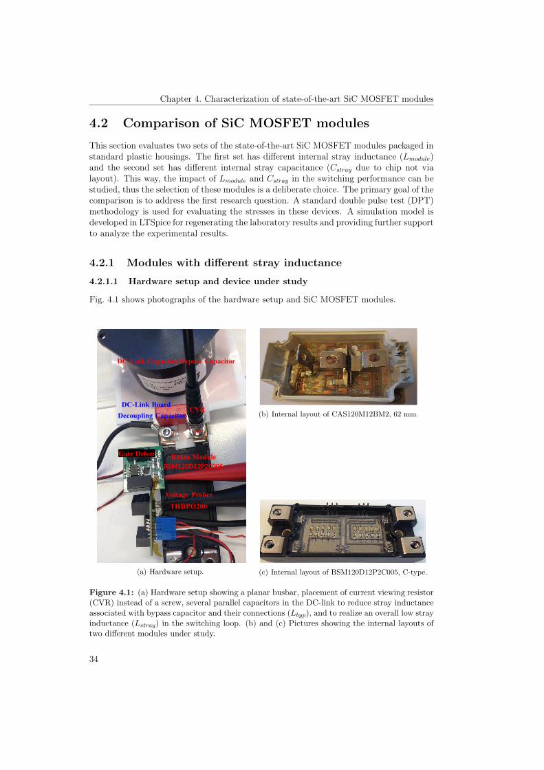
Chapter 4. Characterization of state-of-the-art SiC MOSFET modules
4.2 Comparison of SiC MOSFET modules
This section evaluates two sets of the state-of-the-art SiC MOSFET modules packaged instandard plastic housings. The first set has different internal stray inductance (Lmodule)and the second set has different internal stray capacitance (Cstray due to chip not vialayout). This way, the impact of Lmodule and Cstray in the switching performance can bestudied, thus the selection of these modules is a deliberate choice. The primary goal of thecomparison is to address the first research question. A standard double pulse test (DPT)methodology is used for evaluating the stresses in these devices. A simulation model isdeveloped in LTSpice for regenerating the laboratory results and providing further supportto analyze the experimental results.
4.2.1 Modules with different stray inductance
4.2.1.1 Hardware setup and device under study
Fig. 4.1 shows photographs of the hardware setup and SiC MOSFET modules.
DC-Link Capacitor/Bypass Capacitor
DC-Link BoardCVR
Voltage Probes
THDPO200
Rohm Module
BSM120D12P2C005
Decoupling Capacitor
Gate Driver
(a) Hardware setup.
(b) Internal layout of CAS120M12BM2, 62 mm.
(c) Internal layout of BSM120D12P2C005, C-type.
Figure 4.1: (a) Hardware setup showing a planar busbar, placement of current viewing resistor(CVR) instead of a screw, several parallel capacitors in the DC-link to reduce stray inductanceassociated with bypass capacitor and their connections (Lbyp), and to realize an overall low strayinductance (Lstray) in the switching loop. (b) and (c) Pictures showing the internal layouts oftwo different modules under study.
34

Chapter 4. Characterization of state-of-the-art SiC MOSFET modules
To evaluate the true switching performance of these devices, the DC-link is realizedwith a planar busbar except the termination parts (needed to facilitate the module con-nection) so that the stray inductance in the switching loop can be kept as low as possible.A current viewing resistor (CVR) SSDN-414-01 (400 MHz, 10 mΩ) from T & M researchis used for measuring the drain-source current (Ids). The CVR replaces one of the screwsin the SiC module as it is mounted directly on the screw terminal. This arrangementdecreases the Lstray even further as one screw hole is eliminated. A picture illustratingthe placement of the CVR in the laboratory setup is provided in Fig. 4.1. A detailedsketch for insertion of CVR between the busbar and the module is depicted in Fig. 4.2.The stray inductance of the bussing structure is calculated using Ansys Q3D extractor,and is 14 nH [29].
The on-state resistance (RDS,on), the total die size, the input capacitance (Ciss) andthe output capacitance (Coss) of two different SiC MOSFET modules, from two differentmanufacturers, Wolfspeed and Rohm, are listed in Table 4.1 [123,124]. Each of them hasa voltage rating of 1.2 kV and a current rating of 120 A.
Shunt stud Negative terminal of module
Isolation layer
Clearance for isolation
Locking nut
BNC monitor
Shunt element
Isolating tube
Current flow
Negative
DC-busbar
( 0.5 mm)
Figure 4.2: Detailed sketch of CVR insertion between the busbar and the module. A clearanceof 0.5 mm is provided for shunt voltage drop on the DC-busbar.
Table 4.1: On-state resistance, total die size, Ciss, and Coss of the modules under study.
Parts RDS,on @25C Total die size Ciss Coss
Half-bridge (mΩ) (mm2) (nF) (nF)CAS120M12BM2 (Wolfspeed) 13 6 × 3.10 × 3.36 6.3 0.88BSM120D12P2C005 (Rohm) 16 5 × 3.00 × 4.40 14 0.9
The variables used are: on-state resistance, RDS,on; and input and output capacitances, Ciss and Coss.
4.2.1.2 Experimental results
Summary of measurements with varying gate resistance: All the turn-on andturn-off switching transients are evaluated for a DC-link voltage of 600 V and a drain-source current of 120 A in each of the SiC MOSFET modules at 25 C. Both the chosenSiC modules are evaluated with varying external gate resistance (Rg,ext). dv/dt and di/dtare measured at 50% of the drain voltage and current. A summary of the measurementstaken during the experiments is provided in Table 4.2 for CAS120M12BM2 and Table 4.3for BSM120D12P2C005. dv/dt and dv/dt∗ are the voltage slew rate per module and
35

Chapter 4. Characterization of state-of-the-art SiC MOSFET modules
the voltage slew rate per chip area, respectively, during the turn-off events, while di/dtand di/dt∗ are the current slew rate per module and the current slew rate per chip area,respectively, during the turn-on events. It is observed from the laboratory measurementsthat the variations in dv/dt with varying Rg,ext are approximately in the same range forboth modules, as shown in Table 4.2 and Table 4.3. Above all, the comparison betweenthe two modules shows that the highest achievable switching speed is roughly35 V/ns and 10 A/ns with the state-of-the-art SiC modules using standardplastic packages, which provided an answer to one of the research questions.
Table 4.2: Summary of laboratory measurements for CAS120M12BM2 (Wolfspeed, MOSFET).
Rg,ext dv/dt di/dt Vos Ios Eon Eoff dv/dt∗ di/dt∗
(Ω) (V/ns) (A/ns) (V) (A) (mJ) (mJ) (V/(ns · cm2)) (A/(ns · cm2))0 34.2 9.8 215 134 0.52 0.53 54.7 15.6
1.95 26.3 7.3 185 101 0.76 1.17 42.0 11.63.9 19.7 5.9 156 79 1.46 1.62 31.5 9.46 14.8 5.8 139 67 2.08 1.67 23.6 9.210 10.4 3.5 106 45 3.10 2.52 16.6 5.612 9.4 3.1 90 43 3.83 2.90 15.0 4.9
Table 4.3: Summary of laboratory measurements for BSM120D12P2C005 (Rohm, MOSFET).
Rg,ext dv/dt di/dt Vos Ios Eon Eoff dv/dt∗ di/dt∗
(Ω) (V/ns) (A/ns) (V) (A) (mJ) (mJ) (V/(ns · cm2)) (A/(ns · cm2))0 35.2 7.01 295 87 0.4 1.04 53.3 10.6
1.95 23.4 3.57 264 49 2.0 1.52 35.4 5.43.9 17.5 2.34 212 36 3.7 1.80 26.5 3.56 14.26 1.92 183 31 5.0 2.17 21.6 2.910 10.4 1.32 147 23 7.4 3.2 15.7 212 9.4 1.15 135 21 8.6 3.6 14.2 1.7
Note: Vos, Ios, Eon, Eoff are: voltage and current overshoots; and turn-on and turn-off energy losses.
Comparison of switching at similar dv/dt and di/dt per chip area: Fig. 4.3 (a)and (b) show the measured switching transients of two different SiC MOSFET modulesat similar dv/dt∗ and di/dt∗, respectively. The frequency of oscillation in the Wolfspeedmodule is 36 MHz, while it is 28 MHz in the the Rohm module, which is indicated byfosc in Fig. 4.3. The lower frequency of oscillation in the Rohm module is primarily dueto higher Lmodule. Alternatively, the voltage overshoot (Vos) during turn-off is causedby switching loop inductance and di/dt at turn-off. Lstray can be estimated by, Vos =Lstray · di/dt. As can be seen in Fig. 4.3 (a), di/dt is similar for each module, thus Vos ∝Lstray. Using this relation, Lmodule is computed to be 15 nH in CAS120, while it is 25.8 nHin BSM120. Moreover, as observed from Fig. 4.3 (b), dv/dt is roughly the same in eachmodule; however, CAS120 has higher current overshoot (Ios) compared to BSM120, whichis essentially because of higher effective junction capacitance of the MOSFETs and anti-parallel diodes in the former module. It is worth mentioning that Lstray oscillates withthis effective capacitance.
36

Chapter 4. Characterization of state-of-the-art SiC MOSFET modules
0 100 200 300 400 500 600time [ns]
-200
0
200
400
600
800
1000
-60
0
60
120
180
240
300
(a) Comparison at similar dv/dt per chip area.
0 100 200 300 400 500 600time [ns]
-200
0
200
400
600
800
1000
-60
0
60
120
180
240
300
(b) Comparison at similar di/dt per chip area.
Figure 4.3: Measurement of switching transients of two different SiC MOSFET modules atsimilar dv/dt per chip area during turn-off and similar di/dt per chip area during turn-on.
Comparison of switching at similar voltage and current overshoot: For com-paring the cases with similar Vos and Ios, the events with the closest values are chosenfrom the summary provided in Table 4.2 and Table 4.3. Fig. 4.4 (a) compares the switch-ing waveforms when these modules have similar Vos. The faster rising waveforms of theWolfspeed module compared to the Rohm clearly indicate that the turn-off losses arehigher in the Rohm module for this case. From laboratory measurements, the turn-offloss for Wolfspeed is 1.17 mJ and for Rohm it is 2.17 mJ, denoted by Eoff in Fig. 4.4 (a).Thus, it is desirable to have a module with lower stray inductance, otherwise it suffersfrom higher turn-off switching loss. Rg,ext of 10 Ω for Wolfspeed and 1.95 Ω for Rohmmodules give almost similar Ios, as exemplified in Fig. 4.4 (b). Laboratory measurementsshow turn-on losses of 3.1 mJ for Wolfspeed and 2.0 mJ for Rohm, specified by Eon inFig. 4.4 (b). Note that the stray inductance effectively works as a turn-on snubber, whichis partly a reason for lower turn-on losses in the Rohm module.
0 100 200 300 400 500 600time [ns]
-200
0
200
400
600
800
1000
-60
0
60
120
180
240
300
(a) Comparison at similar voltage overshoot.
0 100 200 300 400 500 600time [ns]
-200
0
200
400
600
800
1000
-60
0
60
120
180
240
300
(b) Comparison at similar current overshoot.
Figure 4.4: Measurement of switching transients of two different SiC MOSFET modules atsimilar voltage overshoot during turn-off and similar current overshoot during turn-on.
37
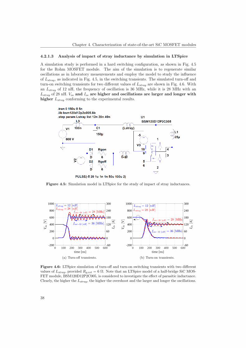
Chapter 4. Characterization of state-of-the-art SiC MOSFET modules
4.2.1.3 Analysis of impact of stray inductance by simulation in LTSpice
A simulation study is performed in a hard switching configuration, as shown in Fig. 4.5for the Rohm MOSFET module. The aim of the simulation is to regenerate similaroscillations as in laboratory measurements and employ the model to study the influenceof Lstray, as indicated in Fig. 4.5, in the switching transients. The simulated turn-off andturn-on switching transients for two different values of Lstray are shown in Fig. 4.6. Withan Lstray of 12 nH, the frequency of oscillation is 36 MHz, while it is 28 MHz with anLstray of 28 nH. Vos and Ios are higher and oscillations are larger and longer withhigher Lstray conforming to the experimental results.
Figure 4.5: Simulation model in LTSpice for the study of impact of stray inductances.
0 100 200 300 400 500 600time [ns]
-200
0
200
400
600
800
1000
-60
0
60
120
180
240
300
(a) Turn-off transients.
0 100 200 300 400 500 600time [ns]
-200
0
200
400
600
800
1000
-60
0
60
120
180
240
300
(b) Turn-on transients.
Figure 4.6: LTSpice simulation of turn-off and turn-on switching transients with two differentvalues of Lstray, provided Rg,ext = 6 Ω. Note that an LTSpice model of a half-bridge SiC MOS-FET module, BSM120D12P2C005, is considered to investigate the effect of parasitic inductance.Clearly, the higher the Lstray, the higher the overshoot and the larger and longer the oscillations.
38

Chapter 4. Characterization of state-of-the-art SiC MOSFET modules
4.2.2 Modules with different stray capacitance
During the research work, it was of interest how the high-voltage SiC MOSFETs differ inswitching compared to the low-voltage SiC MOSFETs. A closer look on the data sheetreadings of SiC MOSFET dies with two different voltage ratings: 1.2 kV and 1.7 kV isprovided in Table 4.4 [125, 126] as an example. Areas and thicknesses are different forthese chips and so are the capacitances. Again, looking into the data sheet readings oftwo similarly rated SiC MOSFET modules in Table 4.5 [127, 128], it is clear that eventhe same rated devices can have different capacitances. Thus, this set of SiC MOSFETmodules with 1.2 kV ratings has been evaluated in the laboratory for the sake of clarifyingthe issue.
Moreover, studying the impact of parasitic capacitances in the switching transientsalso provides an insight into the potential consequences of externally inserted parasiticcapacitances, for instance: addition of a small capacitor or a voltage probe at gate-source;addition of an external anti-parallel diode across the drain-source, as it has a junctioncapacitance; and placement of the gate driver and module, as it can form a parallel tracebetween the gate and drain, and thereby form a capacitance across it.
Table 4.4: Data sheet readings of SiC MOSFET dies with different voltage ratings.
Parameters / Die CPM2-1200-0040B CPM2-1700-0045BVoltage rating (kV) 1.2 1.7Chip size (mm × mm) 3.10 × 5.90 4.08 × 7.35Thickness (µm) 180 ± 40 380 ± 40Ciss (pF) @ 1000 V 1893 3672Coss (pF) @ 1000 V 150 171Crss (pF) @ 1000 V 10 6.7
Table 4.5: Data sheet readings of SiC MOSFET modules with same voltage ratings.
Parameters / ModuleCAS300M12BM2 APTSM120AM09CD3AG
Wolfspeed (MOSFET) Microsemi (MOSFET)Voltage rating (kV) 1.2 1.2No. of chips × (mΩ) 6 × 25 9 × 80Ciss (nF) @ 600 V 11.7 23Coss (nF) @ 600 V 2.55 1.1Crss (nF) @ 600 V 0.07 0.18Qc (nC) @ 600 V 3200 1080Qg (nC) @ 600 V 1025 1224Qgd (nC) @ 600 V 475 360FOM1 = RDS,on × Qg 4270 10880
FOM2 =√RDS,on ×Qgd 44 56
The variables used in Table 4.5 are: input capacitance, Ciss; output capacitance, Coss; reverse transfercapacitance, Crss; capacitive charge of SiC diode, Qc; total gate charge, Qg; and gate-drain charge, Qgd.The conduction figure-of-merit, FOM1; and the switching figure-of-merit, FOM2 are defined in [129].FOM1 and FOM2 are larger by a factor of 2.55 and 1.27, respectively, for APTSM120AM09CD3AG withregard to CAS300M12BM2. A smaller FOM indicates better device performance, i.e., lower device loss.
39
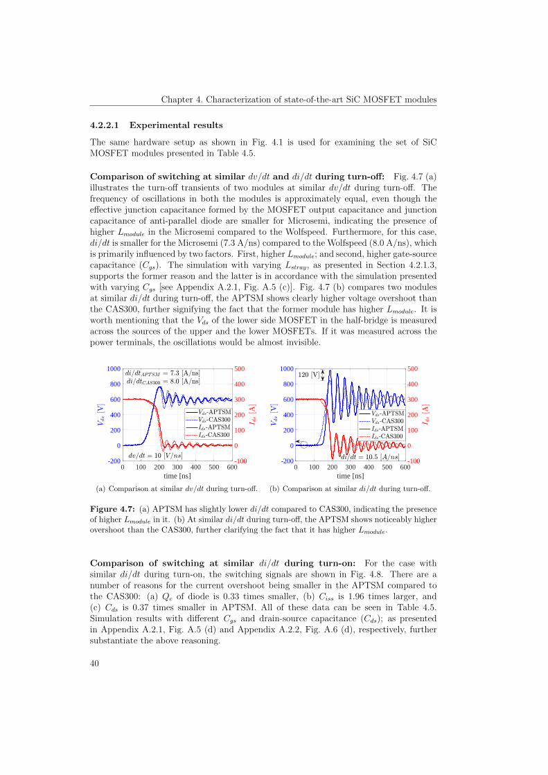
Chapter 4. Characterization of state-of-the-art SiC MOSFET modules
4.2.2.1 Experimental results
The same hardware setup as shown in Fig. 4.1 is used for examining the set of SiCMOSFET modules presented in Table 4.5.
Comparison of switching at similar dv/dt and di/dt during turn-off: Fig. 4.7 (a)illustrates the turn-off transients of two modules at similar dv/dt during turn-off. Thefrequency of oscillations in both the modules is approximately equal, even though theeffective junction capacitance formed by the MOSFET output capacitance and junctioncapacitance of anti-parallel diode are smaller for Microsemi, indicating the presence ofhigher Lmodule in the Microsemi compared to the Wolfspeed. Furthermore, for this case,di/dt is smaller for the Microsemi (7.3 A/ns) compared to the Wolfspeed (8.0 A/ns), whichis primarily influenced by two factors. First, higher Lmodule; and second, higher gate-sourcecapacitance (Cgs). The simulation with varying Lstray, as presented in Section 4.2.1.3,supports the former reason and the latter is in accordance with the simulation presentedwith varying Cgs [see Appendix A.2.1, Fig. A.5 (c)]. Fig. 4.7 (b) compares two modulesat similar di/dt during turn-off, the APTSM shows clearly higher voltage overshoot thanthe CAS300, further signifying the fact that the former module has higher Lmodule. It isworth mentioning that the Vds of the lower side MOSFET in the half-bridge is measuredacross the sources of the upper and the lower MOSFETs. If it was measured across thepower terminals, the oscillations would be almost invisible.
0 100 200 300 400 500 600time [ns]
-200
0
200
400
600
800
1000
-100
0
100
200
300
400
500
(a) Comparison at similar dv/dt during turn-off.
0 100 200 300 400 500 600time [ns]
-200
0
200
400
600
800
1000
-100
0
100
200
300
400
500
(b) Comparison at similar di/dt during turn-off.
Figure 4.7: (a) APTSM has slightly lower di/dt compared to CAS300, indicating the presenceof higher Lmodule in it. (b) At similar di/dt during turn-off, the APTSM shows noticeably higherovershoot than the CAS300, further clarifying the fact that it has higher Lmodule.
Comparison of switching at similar di/dt during turn-on: For the case withsimilar di/dt during turn-on, the switching signals are shown in Fig. 4.8. There are anumber of reasons for the current overshoot being smaller in the APTSM compared tothe CAS300: (a) Qc of diode is 0.33 times smaller, (b) Ciss is 1.96 times larger, and(c) Cds is 0.37 times smaller in APTSM. All of these data can be seen in Table 4.5.Simulation results with different Cgs and drain-source capacitance (Cds); as presentedin Appendix A.2.1, Fig. A.5 (d) and Appendix A.2.2, Fig. A.6 (d), respectively, furthersubstantiate the above reasoning.
40

Chapter 4. Characterization of state-of-the-art SiC MOSFET modules
0 100 200 300 400 500 600time [ns]
-200
0
200
400
600
800
1000
-100
0
100
200
300
400
500
Figure 4.8: Measured turn-on transients of two modules at similar di/dt in the turn-on.Simulation results with different Cgs and Cds, as presented in the Appendix, further confirmthat the lower current overshoot in APTSM is due to smaller Qc, smaller Cds and larger Cgs init compared to CAS300.
4.2.2.2 Analysis of the impact of stray capacitance by simulation in LTSpice
A simulation model is built in LTSpice for studying the impact of Cgs, Cds, and Cgd. Thevalues are chosen as per the data sheet of the chosen modules, as listed in Table 4.5.The simulated turn-off and turn-on transients of the currents and voltages in both thegate and drain sides with different Cgs, Cds, and Cgd are elaborated in Appendix A.2. Inparticular, the comprehensive parametric study can be utilized to anticipate the relativeperformance differences between the devices with the same or different voltage ratings.Hence, this provides a guideline for choosing an appropriate SiC module. Fig. 4.9 (a) and(b) show the simulated turn-off signals: gate-source voltage, Vgs; and gate-source current,Igs, with varying Cgs and Cgd; respectively. Cgs mainly determines the time constant of
time [ns]0 100 200 300 400 500 600
-30
-20
-10
0
10
20
30Vgs @ Cgs = 0 [nF]Vgs @ Cgs = 23 [nF]10× Igs @ Cgs = 0 [nF]10× Igs @ Cgs = 23 [nF]
(a) Gate signals with different Cgs during turn-off.
time [ns]0 100 200 300 400 500 600
-30
-20
-10
0
10
20
30Vgs @ Cgd = 0 [nF]Vgs @ Cgd = 0.18 [nF]10× Igs @ Cgd = 0 [nF]10× Igs @ Cgd = 0.18 [nF]
(b) Gate signals with different Cgd during turn-off.
Figure 4.9: (a) Impact of different Cgs and Cgd on Vgs and Igs. Higher Cgs leads to cleaner gatesignals; whereas, higher Cgd results in noisier ones. Hence, higher ratio of Cgs/Cgd is preferableto avoid possible device malfunction.
41

Chapter 4. Characterization of state-of-the-art SiC MOSFET modules
gate circuit. Higher Cgs reduces the slew rates, mitigates the oscillations and prolongsthe delay times of Vgs. In contrast, higher Cgd aggravates the oscillations. In fact, fasterdv/dt of SiC MOSFET couples power circuit noise to gate side via Cgd. This noise canexceed the threshold voltage limit of SiC MOSFET and cause unwanted turn-on of thedevice. Hence, it is not only the absolute value of Cgd that endangers MOSFET, instead,it is more precisely related to the ratio of Cgs/Cgd. Thus, a MOSFET with higher Cgs/Cgd
ratio should be chosen to avoid such a turn-on.Thus, the simulations and experimental results from Section 4.2 show that the
parasitic components of power MOSFETs limit their fast dynamic perfor-mances; i.e., these parasitics slow down SiC devices, stress them with higher current andvoltage overshoots, and higher losses.
4.3 Comparison of SiC MOSFET and Si IGBT
This section has two parts. The first part compares the state-of-the-art SiC MOSFETmodule and modern Si non-punch-through (NPT) IGBT module under a series of differentconditions, such as similar dv/dt per chip area, similar di/dt per chip area, and similarvoltage and current overshoots. The second part compares further sets of DUTs, six-pack SiC MOSFET module and six-pack Si soft-punch-through (SPT) IGBT moduleunder different loading conditions and junction temperatures. All the chosen modules arecommercially available in standard plastic packages and each set has the same voltageand current ratings.
4.3.1 SiC MOSFET vs. Si non-punch-through IGBT modules
The key characterizing parameters, such as chip size, chip thickness, on-state resistanceof MOSFET / IGBT (RDS,on/RCE,on), on-state resistance of diode (Rd), on-state kneevoltage of IGBT (VCEO) and diode (VFO), Ciss, Coss, Crss, Qc and reverse-recovery charge(Qrr) of anti-parallel diodes in SiC MOSFET and Si IGBT respectively, total gate charge(Qg) and internal gate resistance (Rg,int) are listed in Table 4.6 [127, 130]. The totaldie size in Si IGBT is larger by a factor of three compared to that in SiC MOSFET. Inaddition, Si has a slightly higher dielectric constant than SiC. Both of these factors lead toa larger capacitance in the Si IGBT compared to the SiC MOSFET module. (A dielectricconstant in Si is 11.9, while it is 10 in 4H-SiC.) An electrical breakdown field ten timeshigher in SiC compared to Si allows for a thinner and shorter drift layer. However, thethickness of chip and area is a trade-off between the RDS,on and the capacitance of thepower MOSFET structure.
4.3.1.1 Experimental results
The same hardware setup as shown in Fig. 4.1 is used for examining the set of SiCMOSFET and Si IGBT modules presented in Table 4.6. All the turn-on and turn-offswitching transients are evaluated for a DC-link voltage of 600 V and a drain-sourcecurrent of 300 A in each of the modules at 25 C. Both the chosen modules are evaluatedwith varying Rg,ext.
42

Chapter 4. Characterization of state-of-the-art SiC MOSFET modules
Table 4.6: Key electrical parameters of SiC MOSFET versus Si NPT IGBT modules.
Parameters / ModuleCAS300M12BM2 SKM400GB125D
Wolfspeed (MOSFET) Semikron (IGBT)No. of chips 6 4Chip size (mm × mm) 4.04 × 6.44 11.08 × 11.08Thickness (µm) 200 180RDS,on/RCE,on (mΩ) @25C 5 6.3RDS,on (mΩ) @125C 7.8 7.6VCEO (V) @25C Absent 1.4VCEO (V) @125C Absent 1.7Rd (mΩ) @25C 2.25 2.7Rd (mΩ) @125C 4.35 3VFO (V) @25C 0.925 1.4VFO (V) @125C 0.83 1.1Ciss (nF) @ 600 V 11.7 22Coss (nF) @ 600 V 2.55 3.30Crss (nF) @ 600 V 0.07 1.2Qrr/Qc (µC) 3.2 45Qg (nC) 1025 2650Rg,int (Ω) 3 1.25
The variables used in Table 4.6 are: on-state resistance of MOSFET / IGBT, RDS,on/RCE,on; on-stateresistance of diode, Rd; on-state knee voltage of IGBT, VCEO; on-state knee voltage of diode, VFO; inputcapacitance, Ciss; output capacitance, Coss; reverse transfer capacitance, Crss; capacitive charge of SiCdiode, Qc; reverse-recovery charge of Si diode, Qrr; total gate charge, Qg; and internal gate resistance ofsemiconductor module, Rg,int.
Summary of measurements with varying gate resistances: A summary of themeasurements taken during the experiments is provided in Table 4.7 for SiC MOSFETand Table 4.8 for Si IGBT. dv/dt and dv/dt∗ are the voltage slew rate per module andthe voltage slew rate per chip area during the turn-off events, while di/dt and di/dt∗ arethe current slew rate per module and current slew rate per chip area during the turn-onevents.
Table 4.7: Summary of laboratory measurements for CAS300M12BM2 (Wolfspeed, MOSFET).
Rg,ext dv/dt di/dt Vos Ios Eon Eoff dv/dt∗ di/dt∗
(Ω) (V/ns) (A/ns) (V) (A) (mJ) (mJ) (V/(ns · cm2)) (A/(ns · cm2))0 19.56 10.93 301 198 1.63 3.74 12.5 6.91 15.12 9.14 260 166 3.87 5.04 9.6 5.8
2.2 13.22 7.1 207 140 5.02 5.76 8.4 4.53.4 10.38 6.56 188 125 7.09 7.7 6.6 4.25 8.55 5.35 136 111 8.56 8.64 5.4 3.4
6.8 7.12 4.46 133 105 11.84 10.78 4.5 2.810 5.4 3.5 102 86 16.61 15.16 3.4 2.212 4.9 2.97 85 65 19.62 17.74 3.1 1.9
The variables in Table 4.7 are: external gate resistance, Rg,ext; voltage and current overshoot, Vos andIos; turn-on and turn-off energy loss, Eon and Eoff ; dv/dt and di/dt per chip size, dv/dt
∗and di/dt
∗.
43

Chapter 4. Characterization of state-of-the-art SiC MOSFET modules
Table 4.8: Summary of laboratory measurements for SKM400GB125D (Semikron, IGBT).
Rg,ext dv/dt di/dt Vos Ios Eon Eoff dv/dt∗ di/dt∗
(Ω) (V/ns) (A/ns) (V) (A) (mJ) (mJ) (V/(ns · cm2)) (A/(ns · cm2))0 16.64 12.2 233 393 3.94 7.68 3.3 2.41 13.23 9.07 270 279 11.9 8.87 2.7 1.8
2.35 9.8 5.7 296 168 24.9 10 2.0 1.13.9 7.32 3.58 276 118 36.2 12.15 1.5 0.74.7 6.57 3.05 270 108 40 13.62 1.3 0.66 5.21 2.41 236 89 49.5 16.4 1.0 0.5
The variables in Table 4.8 are: external gate resistance, Rg,ext; voltage and current overshoot, Vos andIos; turn-on and turn-off energy loss, Eon and Eoff ; dv/dt and di/dt per chip size, dv/dt
∗and di/dt
∗.
Comparison of switching at similar dv/dt and di/dt per chip area: Fig 4.10 (a)and (b) compare switching transients of SiC MOSFET versus Si IGBT at similar dv/dt∗
and di/dt∗. Apparently, SiC MOSFET incurs higher losses compared to Si IGBT forthe equal chip sizes. As a consequence, the former module will have a higher junctiontemperature; i.e., the power loss density in SiC is considerably higher. Moreover,for the same chip sizes, the SiC device provides a higher current rating than that of a Sidevice. Hence, a SiC device is anticipated to have a larger thermal ripple, and thus theprobability of failure due to bond wire lift-off and solder fatigue will be higher. This alsodemands a more stringent requirement for the package materials compared to Si.
0 100 200 300 400 500 600time [ns]
-200
0
200
400
600
800
1000
-200
0
200
400
600
800
1000
(a) Turn-off at similar dv/dt per chip size.
0 100 200 300 400 500 600time [ns]
-200
0
200
400
600
800
1000
-200
0
200
400
600
800
1000
(b) Turn-on at similar di/dt per chip size.
Figure 4.10: Measurement of switching transients of SiC MOSFET module versus Si IGBTmodule at similar dv/dt per chip area during turn-off and similar di/dt per chip area duringturn-on. Provided the same chip area, SiC MOSFET incurs higher losses compared to Si IGBT,indicating the possible higher junction temperature in the chip of the former module.
Comparison of switching at similar voltage and current overshoots: Fig 4.11(a) and (b) exemplify the measured switching events at similar Vos during turn-off andsimilar Ios during turn-on. The turn-off energy loss is higher by a factor of 1.75 in theSi IGBT compared to the SiC MOSFET while keeping similar Vos. A comparison at
44

Chapter 4. Characterization of state-of-the-art SiC MOSFET modules
similar Ios for these modules shows that the Si IGBT entails higher turn-on energy loss,a factor of 6.4 higher in Si IGBT compared to SiC MOSFET. The tail current inIGBT functions partly as a turn-off snubber, resulting in lower or no ringing.However, the MOSFET is a unipolar device and has no tail current, thus the amount ofparasitic ringing is markedly higher.
0 100 200 300 400 500 600time [ns]
-200
0
200
400
600
800
1000
-200
0
200
400
600
800
1000
(a) Comparison at similar voltage overshoot.
0 100 200 300 400 500 600time [ns]
-200
0
200
400
600
800
1000
-200
0
200
400
600
800
1000
(b) Comparison at similar current overshoot.
Figure 4.11: Measurement of switching transients of SiC MOSFET versus Si IGBT modulesat similar voltage overshoot during turn-off and similar current overshoot during turn-on. Giventhe similar overshoot, SiC MOSFET shows better performance than Si IGBT from an efficiencyviewpoint, but the amount of parasitic ringing is noticeably higher in SiC MOSFET. Note thatturn-on losses are higher in Si IGBT which is primarily because of the higher recovery charge ofSi pn diode associated with it.
Comparison of switching loss in SiC MOSFET versus Si IGBT: From Table 4.8,it is evident that Vos of the Si IGBT increases with gate resistance during turn-off (Rg,off ),reaches a peak value and then decreases again. Therefore, Rg,off of 0 Ω is chosen as anoptimized value, which also gives the lowest loss. As a trade-off between Ios and turn-onlosses, Rg,on of 2.35 Ω is chosen. Considering ringing, switching losses and overshoots,Rg,on of 5 Ω and Rg,off of 3.4 Ω are chosen for the SiC MOSFET. Table 4.9 shows thespecific switching energy loss for the selected gate resistances. The turn-off loss turns outto be equal for both modules, whereas the turn-on loss in the SiC MOSFET is 1/3 timesthat of the Si IGBT. The specific reverse-recovery loss of SiC diode (Err−spec) is 1/8.76times that of Si diode. Fig. 4.12 displays the switching transients for an optimal case.
Table 4.9: Specific loss of SiC MOSFET versus Si IGBT for the selected Rg,on and Rg,off .
Half-bridge partsRg,on Rg,off Eon−spec Eoff−spec Err−spec
(Ω) (Ω) (µJ/A) (µJ/A) (µJ/A)SiC MOSFET 5 3.4 28.5 25.6 1.3Si IGBT 2.35 0 83 25.6 11.4
The variables used in Table 4.9 are: turn-on and turn-off gate resistance, Rg,on and Rg,off ; specificswitching energy loss of transistor during turn-on and turn-off, Eon−spec and Eoff−spec; and specificreverse-recovery energy loss of diode, Err−spec.
45

Chapter 4. Characterization of state-of-the-art SiC MOSFET modules
0 100 200 300 400 500 600time [ns]
-200
0
200
400
600
800
1000
-200
0
200
400
600
800
1000
(a) Turn-off transients.
0 100 200 300 400 500 600time [ns]
-200
0
200
400
600
800
1000
-200
0
200
400
600
800
1000
(b) Turn-on transients.
Figure 4.12: Comparison of switching events for the chosen optimal case.
4.3.2 SiC MOSFET versus Si soft-punch-through IGBT
4.3.2.1 Device under test and hardware setup
A photograph of a six-pack module is provided in Fig. 4.13 (a). For achieving higheroutput power, three bridge-legs of the modules are paralleled forming a single half-bridgeconfiguration, a schematic diagram of which is shown in Fig. 4.13 (b). In order to havea comparable stray inductance as in a real application circuit, a three-phase inverterpower circuit board, acting as a stripline connection between the module and the DC-linkcapacitors, is built, and a six-pack module is mounted such that the three bridge-legs areparalleled outside the module.
(a) Six-pack MOSFET module. (b) Schematic diagram.
Figure 4.13: (a) Photograph of a six-pack SiC MOSFET module from Wolfspeed. (b)Schematic diagram showing the parallel connection of three phases in a six-pack SiC MOSFETmodule forming an equivalent single phase (1-ph), 150 A, half-bridge configuration.
Table 4.10 shows the key electrical parameters of the SiC MOSFET versus the SiIGBT taken from the manufacturer’s data sheet [131, 132]. Both the modules have samepackaging and voltage rating (1.2 kV). A complete laboratory setup showing the DPTmeasurement is depicted in Fig. 4.14. The Si IGBT is driven by the same gate driver asthat of the SiC MOSFET, except for a small modification for obtaining ±15 V requiredfor driving an IGBT.
46

Chapter 4. Characterization of state-of-the-art SiC MOSFET modules
Table 4.10: Key electrical parameters of SiC MOSFET versus Si SPT IGBT modules.
Parameters / ModuleCCS050M12CM2 FS75R12KT4 B15
Wolfspeed (MOSFET) Infineon (IGBT)RDS,on / RCE,on (mΩ) @25C 25 11.1RDS,on (mΩ) @125C 39.4 15.51VCEO (V) @25C Absent 1VCEO (V) @125C Absent 0.84Rd (mΩ) @25C 10 9.46Rd (mΩ) @125C 19.77 10.62VFO (V) @25C 0.85 1.05VFO (V) @125C 0.77 0.93Ciss (nF) @ 600 V 2.81 4.3Coss (nF) @ 600 V 2.55 3.30Crss (nF) @ 600 V 0.014 0.16Qrr/Qc (µC) 0.28 16Qg (nC) 180 570Rg,int (Ω) 1.5 10Vgs,th / Vge,th (V) 2.3 5.8Vgs / Vge (V) +20/-5 ±15Lmodule (nH) 30 19
The variables used in Table 4.10 are: on-state resistance of MOSFET / IGBT, RDS,on/RCE,on; on-stateresistance of diode, Rd; on-state knee voltage of IGBT, VCEO; on-state knee voltage of diode, VFO; inputcapacitance, Ciss; output capacitance, Coss; reverse transfer capacitance, Crss; capacitive charge of SiCdiode, Qc; reverse-recovery charge of Si diode, Qrr; total gate charge, Qg; internal gate resistance ofsemiconductor module, Rg,int; gate-source or gate-emitter threshold voltage, Vgs,th / Vge,th; gate-sourceor gate-emitter, Vgs / Vge; and internal stray inductance of module, Lmodule.
Double-pulse generatorOscilloscope
Single-layer inductor
Three-phase inverter card
Figure 4.14: Hardware setup showing the double pulse test arrangement. Switching energyloss is measured using a three-phase inverter power circuit board in order to emulate a strayinductance of a real application circuit.
47

Chapter 4. Characterization of state-of-the-art SiC MOSFET modules
4.3.2.2 Measurement results
Switching transients with varying load current: In this section, the DC-link volt-age is set to 500 V while the load current is increased from 30 A to 150 A. It can beobserved from Fig. 4.15 that the di/dt of the current in the SiC MOSFET and the diode
0 200 400 600 800 1000 1200time [ns]
-100
102030405060708090
Dra
in C
urre
nt [
A]
30 A60 A90 A120 A150 A
(a) Turn-on transient of the MOSFET.
0 200 400 600 800 1000 1200time [ns]
-100
102030405060708090
Col
lect
or C
urre
nt [
A]
30 A60 A90 A120 A150 A
(b) Turn-on transient of the IGBT.
0 200 400 600 800 1000 1200time [ns]
-10
0
10
20
30
40
50
60
70
Dra
in V
olta
ge [
V]
30 A60 A90 A120 A150 A
(c) Turn-off transient of the MOSFET.
0 200 400 600 800 1000 1200time [ns]
-10
0
10
20
30
40
50
60
70
Col
lect
or V
olta
ge [
V]
30 A60 A90 A120 A150 A
(d) Turn-off transient of the IGBT.
0 200 400 600 800 1000 1200time [ns]
-40-30-20-10
0102030405060
Dio
de C
urre
nt [
A]
30 A60 A90 A120 A150 A
(e) Turn-off transient of the SiC JBS.
0 200 400 600 800 1000 1200time [ns]
-40-30-20-10
0102030405060
Dio
de C
urre
nt [
A]
30 A60 A90 A120 A150 A
(f) Turn-off transient of the Si diode.
Figure 4.15: Drain-source/collector-emitter current, drain-source/collector-emitter voltageand diode current with varying load current for the SiC MOSFET versus the Si IGBT.
48

Chapter 4. Characterization of state-of-the-art SiC MOSFET modules
increases slightly, while the dv/dt of the MOSFET voltage increases noticeably. This as-pect of the part of behavior in the SiC MOSFET also corresponds to that of the Si IGBT.However, the peak reverse current of the SiC anti-parallel diode remains almostconstant at all the load currents, which is depicted in Fig. 4.15 (e). Conversely, thepeak reverse-recovery current of the Si anti-parallel diode increases with theincrease of the load current, which is apparent from Fig. 4.15 (f). This exemplifies aclear benefit of using a SiC JBS diode instead of a Si pn diode as the switching behaviorof the former remains intact irrespective of the output power.
Switching transients with varying junction temperature: In this section, the DC-link voltage is set to 500 V and the load current to 120 A while the junction temperatureis increased from 25 C to 125 C. With the increased temperature, the turn-on of SiCMOSFET becomes slightly faster, as depicted in Fig. 4.16. This is because of the negativetemperature coefficient of gate threshold voltage, and therefore leads to a decrease in theturn-on switching energy loss. The SiC MOSFET module is co-packed with the SiCJunction barrier Schottky (JBS) diode as an anti-parallel diode. The reverse-recoverycharge in the SiC SBD is extremely low compared to the Si diode [133]. This charge is notdue to conductivity modulation as in Si diode and is independent of temperature, forwardcurrent and di/dt as inferred from these characterization and also conforms with [134].
0 200 400 600 800 1000 1200time [ns]
-20-10
0102030405060708090
(a) Turn-on transient of the MOSFET.
0 200 400 600 800 1000 1200time [ns]
-20-10
0102030405060708090
(b) Turn-on transient of the IGBT.
0 200 400 600 800 1000 1200time [ns]
-20
-10
0
10
20
30
40
50
60
70
(c) Turn-off transient of the MOSFET.
0 200 400 600 800 1000 1200time [ns]
-20
-10
0
10
20
30
40
50
60
70
(d) Turn-off transient of the IGBT.
49

Chapter 4. Characterization of state-of-the-art SiC MOSFET modules
0 200 400 600 800 1000 1200time [ns]
-50-40-30-20-10
0102030405060
(e) Turn-off transient of the SiC JBS.
0 200 400 600 800 1000 1200time [ns]
-50-40-30-20-10
0102030405060
(f) Turn-off transient of the Si diode.
Figure 4.16: Drain-source/collector-emitter current, drain-source/collector-emitter voltageand diode current with varying junction temperature for the SiC MOSFET versus the Si IGBTmodules. Measured results illustrate that the reverse-recovery current of Si-pn diode and tailcurrent of IGBT show strong temperature dependency while the characteristics of the SiC MOS-FET and SiC diode remain less affected.
In the Si IGBT module, the Si diode is present as a freewheeling diode. It is evidentfrom Fig. 4.16 (b) and (f) that the reverse-recovery current present at turn-off of thediode directly affects the current peak during the turn-on of the Si IGBT. This peakworsens with increased operating temperature. During the turn-off, the voltage overshootdecreases a little as the turn-off voltage rise slows down with increased temperature, asseen in Fig. 4.16 (d).
Table 4.11 shows a sample of key switching energy loss measurements for the SiCMOSFET versus the Si IGBT with a DC-link voltage of 500 V and a load current of120 A at two different junction temperatures: 25 C and 125 C and two different gate
Table 4.11: Key measurements of SiC MOSFET vs Si IGBT module. Vds = 500 V, Ids =120 A, two different junction temperatures: Tj = 25 C and Tj = 125 C, and two different gateresistances for each modules.
Device Under Test (DUT) Tj Rg,ext dv/dt di/dt Eoff Eon Err
(C ) (Ω) (V/ns) (A/ns) (mJ) (mJ) (mJ)CCS050M12CM2 (Wolfspeed) 25 20 8.49 2.63 1.28 3.26 0.22
25 36.5 4.25 1.33 3.86 6.95 0.11125 20 8 2.89 1.54 2.57 0.35125 36.5 4.08 1.5 4.08 6.28 0.12
FS75R12KT4 B15 (Infineon) 25 12.2 4.37 2.28 6 8.43 2.4625 20 4.42 1.43 6.36 14.13 2.34125 12.2 2.7 2.41 10.67 12.9 9.37125 20 2.4 1.5 10.36 18.36 7.7
The variables used in Table 4.11 are: device junction temperature, Tj ; external gate resistance, Rg,ext;switching energy loss of transistor during turn-on and turn-off, Eon and Eoff ; and reverse-recovery energyloss of diode, Err.
50

Chapter 4. Characterization of state-of-the-art SiC MOSFET modules
resistances for each modules. dv/dt is the voltage slew rate during turn-off and di/dt isthe current slew rate during turn-on of the DUT. The Eoff in the Si IGBT is relativelyhigh and is almost similar at both high (20 Ω) and low (12.2 Ω) Rg,ext. This is primarilygoverned by the intrinsic phenomenon within the IGBT structure. In particular, this is aresult of the recombination process and the charge carrier lifetime being independent ofRg,ext.
On the other hand, the Eoff of the SiC MOSFET decreases remarkably with decreasein Rg,ext, which is principally because of the unipolar nature of the device. The Eon
of both devices depends strongly on Rg,ext. The Err in both the Si and SiC diodesdecreases slightly with increasing Rg,ext. With the increase in temperature, Err increasessubstantially in the Si diode, whereas it is slightly increased or almost unaffected by thetemperature in the SiC JBS. Further, at similar dv/dt of roughly 4.3 V/ns, Eoff of SiIGBT is 1.5 times higher compared to that of SiC MOSFET, which is primarily becauseof the longer tail current that SPT IGBT exhibits.
4.4 Summary
The chapter has focused on the characterization of the state-of-the-art SiC MOSFET andSi IGBT modules, the summary of which are listed as follows:
1. The highest achievable dv/dt and di/dt with SiC MOSFET modules are roughly35 V/ns and 10 A/ns for 120 A ratings and about 20 V/ns and 11 A/ns for 300 Aratings. Similarly, with the Si IGBT module the maximum dv/dt and di/dt measuredat 300 A are about 17 V/ns and di/dt is 12 A/ns. This information was missing inthe data sheet of the modules.
2. Both the simulation and laboratory results illustrate that higher stray parametershinder utilization of the fast switching potential of SiC power modules; i.e., theseparasitics slow down SiC devices and stress them with higher current and voltageovershoots, and higher losses.
3. A closer look into gate waveforms while varying gate-source capacitance show thathigher values reduce ringing and maintain the gate loop stability. Conversely, highergate-drain capacitance together with fast dv/dt can cause unwanted turn-on of thedevice owing to the fact that dv/dt related noise exceeds the threshold voltage limit ofthe SiC MOSFET. Overall, it is apparent that not only gate-drain capacitance but alsothe ratio of gate-source to gate-drain capacitance are responsible for the malfunctionof the device, and this ratio should be kept high to avoid it.
4. The switching phenomenon of the SiC MOSFET is almost independent of the oper-ating temperature, while there is a strong temperature dependence in the Si IGBT.In particular, the reverse-recovery current of the Si diode and the tail current of theIGBT worsens with increase in temperature.
5. A clear benefit of using SiC JBS diode instead of Si pn diode is exemplified as theswitching behavior of the former remains intact irrespective of the loading conditions,such as higher output power and higher junction temperatures while the performanceof the latter worsens with the same conditions.
51

Chapter 4. Characterization of state-of-the-art SiC MOSFET modules
52

Chapter 5
Characterization of body-diodes instate-of-the-art SiC MOSFETs
The information presented in this chapter is based on publication C6, the primary objectiveof which is to answer the following research question.
Q 1. Are the body-diodes in SiC MOSFETs good enough as freewheeling diodes?
5.1 Introduction
In power electronics applications, such as motor drives, synchronous rectifiers, phaseshift PWM DC-DC power converters, an anti-parallel or a freewheeling diode is requiredacross a semiconductor switching device to handle the current in the reverse direction. AMOSFET structure exhibits an intrinsic body-diode which has a structure of a PiN diode.In a SiC MOSFET, this PiN diode has a very high forward voltage drop (VF = 4.8 V atVgs = -5 V, IF = 20 A, 25 C [135]) because SiC has a wider bandgap energy (≈ 3 eV)compared to Si (≈ 1.2 eV). However, VF in a SiC Schottky diode is significantly lower(1.8 V, IF = 20 A, 25 C) [136] as it is determined by the metal semiconductor barrierheight instead of a p+n junction barrier in the PiN diode [45].
There are different perspectives presented in the available literature in different time-frames. For example, in [137] the use of the body-diode is not recommended; instead,an external Schottky diode is suggested because of its high VF . In other words, thePiN-structure of the parasitic-diode in the SiC MOSFET was not optimized for lowerlosses. Then the data sheet of the manufacturer would contain very limited informationabout the body-diode and that limited information would be presented at low di/dt (forinstance 0.1 A/ns) [138]. There has been continuous improvement in the performanceof the body-diode and the data sheets have been also updated accordingly. In the syn-chronous rectifier operation, the MOSFET channel is turned on in the reverse conductingmode so that the major part of the current flows through this channel and only a partthrough the body-diode. Alternatively stated, the MOSFET shunts the conduction phasecurrent away from the body-diode reducing the conduction losses caused by the highVF . Results with similar operations as that of Si MOSFET were also presented for SiCMOSFET in [139]. Thereafter, Wolfspeed have updated their data sheet for the secondgeneration MOSFETs with higher di/dt of 2.4 A/ns [135] along with the third-quadrantcharacteristics as an addendum compared to its first generation MOSFET [138]. Look-ing further in various publications, eliminating the anti-parallel diode and using only the
53
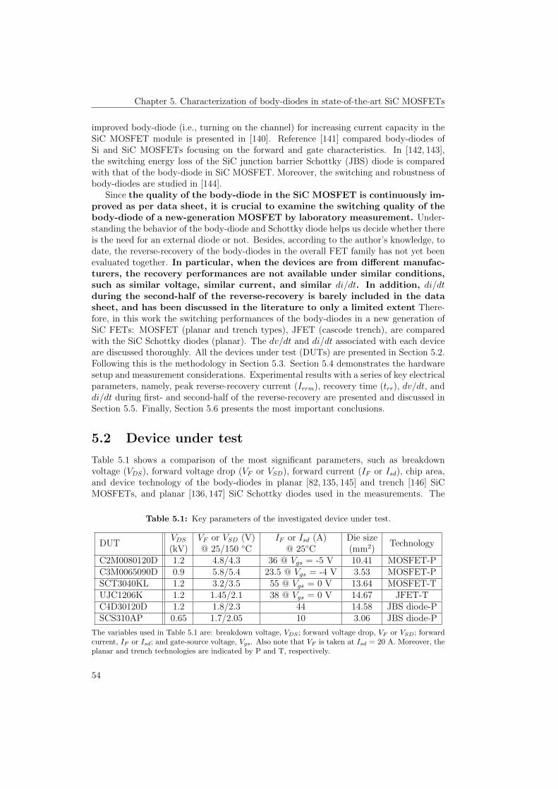
Chapter 5. Characterization of body-diodes in state-of-the-art SiC MOSFETs
improved body-diode (i.e., turning on the channel) for increasing current capacity in theSiC MOSFET module is presented in [140]. Reference [141] compared body-diodes ofSi and SiC MOSFETs focusing on the forward and gate characteristics. In [142, 143],the switching energy loss of the SiC junction barrier Schottky (JBS) diode is comparedwith that of the body-diode in SiC MOSFET. Moreover, the switching and robustness ofbody-diodes are studied in [144].
Since the quality of the body-diode in the SiC MOSFET is continuously im-proved as per data sheet, it is crucial to examine the switching quality of thebody-diode of a new-generation MOSFET by laboratory measurement. Under-standing the behavior of the body-diode and Schottky diode helps us decide whether thereis the need for an external diode or not. Besides, according to the author’s knowledge, todate, the reverse-recovery of the body-diodes in the overall FET family has not yet beenevaluated together. In particular, when the devices are from different manufac-turers, the recovery performances are not available under similar conditions,such as similar voltage, similar current, and similar di/dt. In addition, di/dtduring the second-half of the reverse-recovery is barely included in the datasheet, and has been discussed in the literature to only a limited extent There-fore, in this work the switching performances of the body-diodes in a new generation ofSiC FETs: MOSFET (planar and trench types), JFET (cascode trench), are comparedwith the SiC Schottky diodes (planar). The dv/dt and di/dt associated with each deviceare discussed thoroughly. All the devices under test (DUTs) are presented in Section 5.2.Following this is the methodology in Section 5.3. Section 5.4 demonstrates the hardwaresetup and measurement considerations. Experimental results with a series of key electricalparameters, namely, peak reverse-recovery current (Irrm), recovery time (trr), dv/dt, anddi/dt during first- and second-half of the reverse-recovery are presented and discussed inSection 5.5. Finally, Section 5.6 presents the most important conclusions.
5.2 Device under test
Table 5.1 shows a comparison of the most significant parameters, such as breakdownvoltage (VDS), forward voltage drop (VF or VSD), forward current (IF or Isd), chip area,and device technology of the body-diodes in planar [82, 135, 145] and trench [146] SiCMOSFETs, and planar [136, 147] SiC Schottky diodes used in the measurements. The
Table 5.1: Key parameters of the investigated device under test.
DUTVDS VF or VSD (V) IF or Isd (A) Die size
Technology(kV) @ 25/150 C @ 25C (mm2)
C2M0080120D 1.2 4.8/4.3 36 @ Vgs = -5 V 10.41 MOSFET-PC3M0065090D 0.9 5.8/5.4 23.5 @ Vgs = -4 V 3.53 MOSFET-PSCT3040KL 1.2 3.2/3.5 55 @ Vgs = 0 V 13.64 MOSFET-TUJC1206K 1.2 1.45/2.1 38 @ Vgs = 0 V 14.67 JFET-TC4D30120D 1.2 1.8/2.3 44 14.58 JBS diode-PSCS310AP 0.65 1.7/2.05 10 3.06 JBS diode-P
The variables used in Table 5.1 are: breakdown voltage, VDS ; forward voltage drop, VF or VSD; forwardcurrent, IF or Isd; and gate-source voltage, Vgs. Also note that VF is taken at Isd = 20 A. Moreover, theplanar and trench technologies are indicated by P and T, respectively.
54

Chapter 5. Characterization of body-diodes in state-of-the-art SiC MOSFETs
body-diode in the trench SiC JFET with cascode configuration [148, 149] is also listedin Table 5.1 to give a complete overview of the diodes in FET technology. Fig. 2.3 inChapter 2 shows the structures of SiC MOSFET with planar versus trench technology.Put simply, trench structures improve the static performances of the devices [46].
5.3 Methodology
The double-pulse test (DPT) methodology is used for accessing the dynamic performanceof a body-diode in a SiC MOSFET. Two pulses are sent to a control device (transistorT1) in a clamped inductive load circuit, as shown in Fig. 5.1 (a), while the gate and sourceof the DUT are either shorted or supplied with -5 V in order to ensure that the DUT isturned-off all the time, and hence, only the body-diode is active in the circuit. Fig. 5.1 (b)displays the typical test waveforms, where the first turn-off (at the end of the first pulse)and the second turn-on (at the beginning of the second pulse) are indicated. Channel 1 isthe gate voltage of the transistor T1 (Vgs−H), Channel 2 is the anode-to-cathode voltageof diode (Vsd), Channel 3 is the source-to-drain current (Isd), and channel 4 is the currentthrough load inductor (IL). By regulating the width of the first pulse and the DC-busvoltage, the desired load current is achieved. Each time only two pulses are applied andthe DUT is switched only twice. As a consequence, the device junction temperature risesdue to the switching loss becomes negligibly small. Thus, the junction temperature canbe controlled externally by the hot plate. A gate voltage of 20 V is applied during turn-onand -5 V during turn-off for the upper MOSFET. In order to use the passive probe andcoaxial shunt for voltage and current measurements; respectively, with the same reference(grounding) as that of the oscilloscope, the body-diode of low side transistor T1 is hard-switched. By varying the external gate resistance (Rg,ext), the slew rates of the currentand voltage across the DUTs are controlled. It should be noted that the internal resistanceof T1 is 7 Ω. Detailed view of first turn-off and the second turn-on events are displayedin Fig. 5.2.
(a) Clamped inductive load test circuit. (b) Typical DPT waveforms.
Figure 5.1: Illustration of a clamped inductive load circuit for hard switching test of body-diodein SiC MOSFET (a), and an example of a typical DPT waveform in (b).
55

Chapter 5. Characterization of body-diodes in state-of-the-art SiC MOSFETs
100 ns/div
gs HV
sdV
sdI
(a) 1st turn-off event of C3M.
gs HV
sdV
sdI
100 ns/div
(b) 2nd turn-on event of C3M.
Figure 5.2: Illustration of the detailed view of the first turn-off and the second turn-on events,as indicated in Fig. 5.1 (b) for C3M MOSFET at 600 V and 20 A. For analyzing the reverse-recovery performance of the DUT, the second turn-on instant, where the transistor is turned-onand the diode is turned-off, is the key point of interest, which will be the focus in the upcomingsections of this chapter for different chosen DUTs. Note that the lower transistor is chosen asa DUT in order to facilitate the current and voltage measurements by shunt and passive probewith the same reference as that of the oscilloscope.
5.4 Hardware setup and measurement considerations
The complete laboratory setup with measurement is illustrated in Fig. 5.3. Double-pulsesare generated using a function generator. Two single-layer winding air core inductors areconnected in series as an inductive load. A printed circuit board (PCB) probe-tip adapteris employed in order to reduce the ground-lead inductance, as shown in Fig. 5.3 (b).
Shunt
Voltage probes
Double-pulse generator
2 single winding inductors in series, 1 pF
Oscilloscope, 1 GHz
Low-voltage DC power supply
(a) Hardware setup.
Current shunt
1 GHz
Probe-tip adapters
Voltage probes
500 MHz &1 GHz
Current probe, 120 MHz
Ferrite core transformer
dsV
gsV
dsI
(b) Measurement arrangements.
Figure 5.3: Laboratory setup showing the arrangement for current and voltage measurementsof the body-diode. The current is measured using a high-bandwidth, low-inductive-currentshunt. The voltage is measured using a high-bandwidth single-ended probe, mounted to thePCB using a probe-tip adaptor for a reduction of the ground-lead inductance.
56

Chapter 5. Characterization of body-diodes in state-of-the-art SiC MOSFETs
5.5 Experimental results
In this section, the reverse-recovery characteristics of the various chosen DUTs are evalu-ated at different operating conditions including the forward current, turn-off voltage, andcurrent commutating slope (di/dt). Moreover, this section is divided into four subsec-tions. Subsection 5.5.1 compares planar versus trench SiC MOSFETs. This is followedby Subsection 5.5.2, which evaluates SiC Schottky diodes with different chip areas. Then,in Subsection 5.5.3, the switching performance of cascode SiC JFET is included. Finally,Subsection 5.5.4 compares the turn-off characteristics of all DUTs at two voltages: 400and 600 V.
5.5.1 Planar versus double-trench MOSFETs
In this subsection, two technologies in SiC MOSFET: planar (C3M) versus double-trench(SCT) are compared. Fig. 5.4 shows the switching waveforms of body-diodes in C3Mversus SCT MOSFETs. Apparently, when Isd through a body-diode increases, Irrmand trr are negligibly affected provided the same Vsd, as can be seen in Fig. 5.4 (a)and (b), unlike that of Si PiN diodes where these parameters significantly increase withincrease in Isd [90] indicating that there is a little or no charge storage mechanismin body-diodes of these SiC MOSFETs. Indeed, there are two fundamentalreasons for smaller stored charges in SiC MOSFETs: first, the lower lifetimeof the minority carrier, and second, the smaller physical area of the die, andhence, smaller area for stored charges in SiC compared to that in Si.
Furthermore, it is also elucidated from Fig. 5.4 that lower the Isd, the greater thedv/dt. Note that dv/dt mainly concerns insulation strain. Examining the experimentalresults in Fig. 5.4 (c) and (d) at Isd of 20 A, it is evident that both Irrm and trrincrease with supply voltage. Actually, higher energy (1/2 · Coss · V 2
sd) is storedat higher voltage, and thus leads to higher charge, which is the reason for anadditional area at higher voltage compared to lower voltage. As can be seen inFig. 5.4 (e) and (f), the smaller gate resistance increases peak of Irrm and di/dt duringthe first-half of recovery (di/dt1). On closer observation, the body-diode in SCT showsnoticeable decrease in di/dt1 with increase in Rg,ext than that in C3M.
0 20 40 60 80 100 120 140 160-20
-10
0
10
20
30
40
-800
-600
-400
-200
0
200
400
(a) Isd variation in body-diode of C3M at 600 V.
0 20 40 60 80 100 120 140 160-20
-10
0
10
20
30
40
-800
-600
-400
-200
0
200
400
(b) Isd variation in body-diode of SCT at 600 V.
57
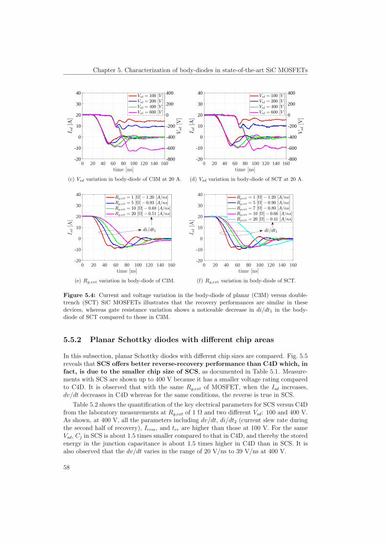
Chapter 5. Characterization of body-diodes in state-of-the-art SiC MOSFETs
0 20 40 60 80 100 120 140 160-20
-10
0
10
20
30
40
-800
-600
-400
-200
0
200
400
(c) Vsd variation in body-diode of C3M at 20 A.
0 20 40 60 80 100 120 140 160-20
-10
0
10
20
30
40
-800
-600
-400
-200
0
200
400
(d) Vsd variation in body-diode of SCT at 20 A.
0 20 40 60 80 100 120 140 160-20
-10
0
10
20
30
40
(e) Rg,ext variation in body-diode of C3M.
0 20 40 60 80 100 120 140 160-20
-10
0
10
20
30
40
(f) Rg,ext variation in body-diode of SCT.
Figure 5.4: Current and voltage variation in the body-diode of planar (C3M) versus double-trench (SCT) SiC MOSFETs illustrates that the recovery performances are similar in thesedevices, whereas gate resistance variation shows a noticeable decrease in di/dt1 in the body-diode of SCT compared to those in C3M.
5.5.2 Planar Schottky diodes with different chip areas
In this subsection, planar Schottky diodes with different chip sizes are compared. Fig. 5.5reveals that SCS offers better reverse-recovery performance than C4D which, infact, is due to the smaller chip size of SCS, as documented in Table 5.1. Measure-ments with SCS are shown up to 400 V because it has a smaller voltage rating comparedto C4D. It is observed that with the same Rg,ext of MOSFET, when the Isd increases,dv/dt decreases in C4D whereas for the same conditions, the reverse is true in SCS.
Table 5.2 shows the quantification of the key electrical parameters for SCS versus C4Dfrom the laboratory measurements at Rg,ext of 1 Ω and two different Vsd: 100 and 400 V.As shown, at 400 V, all the parameters including dv/dt, di/dt2 (current slew rate duringthe second half of recovery), Irrm, and trr are higher than those at 100 V. For the sameVsd, Cj in SCS is about 1.5 times smaller compared to that in C4D, and thereby the storedenergy in the junction capacitance is about 1.5 times higher in C4D than in SCS. It isalso observed that the dv/dt varies in the range of 20 V/ns to 39 V/ns at 400 V.
58
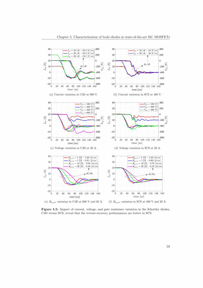
Chapter 5. Characterization of body-diodes in state-of-the-art SiC MOSFETs
0 20 40 60 80 100 120 140 160-20
-10
0
10
20
30
40
-800
-600
-400
-200
0
200
400
(a) Current variation in C4D at 600 V.
0 20 40 60 80 100 120 140 160time [ns]
-20
-10
0
10
20
30
40
-800
-600
-400
-200
0
200
400
(b) Current variation in SCS at 400 V.
0 20 40 60 80 100 120 140 160time [ns]
-20
-10
0
10
20
30
40
-800
-600
-400
-200
0
200
400
(c) Voltage variation in C4D at 20 A.
0 20 40 60 80 100 120 140 160-20
-10
0
10
20
30
40
-800
-600
-400
-200
0
200
400
(d) Voltage variation in SCS at 20 A.
0 20 40 60 80 100 120 140 160time [ns]
-20
-10
0
10
20
30
40
(e) Rg,ext variation in C4D at 600 V and 20 A.
0 20 40 60 80 100 120 140 160-20
-10
0
10
20
30
40
(f) Rg,ext variation in SCS at 400 V and 20 A.
Figure 5.5: Impact of current, voltage, and gate resistance variation in the Schottky diodes,C4D versus SCS, reveal that the reverse-recovery performances are better in SCS.
59

Chapter 5. Characterization of body-diodes in state-of-the-art SiC MOSFETs
Table 5.2: dv/dt, di/dt2, Irrm, and trr of C4D and SCS at 20 A and two different voltages:100 and 400 V.
(a) dv/dt, di/dt2, Irrm, and trr at 100 V.
DUTVsd = 100 V
Cj dv/dt di/dt2 Irrm trr(pF) (V/ns) (A/ns) (A) (ns)
SCS310AP 90 19.7 0.29 2.46 24C4D30120D 138 17.9 0.51 5.68 23
(b) dv/dt, di/dt2, Irrm, and trr at 400 V.
DUTVsd = 400 V
Cj dv/dt di/dt2 Irrm trr(pF) (V/ns) (A/ns) (A) (ns)
SCS310AP 48 39.0 0.36 6.66 43C4D30120D 70 19.8 0.55 8.93 46
The variables used in Table 5.2 are: junction capacitance of Schottky diode, Cj ; anode-to-cathode voltageof diode, Vsd; voltage slew rate of Vsd, dv/dt; current slew rate during second-half of reverse-recovery,di/dt2; peak reverse-recovery current, Irrm; and reverse-recovery time, trr.
5.5.3 Trench cascode JFET
In this subsection, the body-diode in trench cascode JFET is discussed. Fig. 5.6 (a)–(c)depicts the turn-off switching performance of JFET. Clearly, it can be observed that theIrrm in the body-diode of SiC JFET decreases as Isd increases and the oppositeis true as Vsd or di/dt increases. It is worth mentioning that the trench SiC JFETdoes not contain a built-in body-diode or any parasitic NPN transistor as seen with SiCMOSFET. However, during the reverse conducting mode, the body-diode of low-voltage(LV) Si MOSFET and the JFET channel provide a current path, as routed by a reddashed line in Fig. 5.6 (d), providing the same functionality like an anti-parallel diode.
0 20 40 60 80 100 120 140 160time [ns]
-20
-10
0
10
20
30
40
-800
-600
-400
-200
0
200
400
(a) Isd variation in body-diodes of UJC at 600 V.
0 20 40 60 80 100 120 140 160time [ns]
-20
-10
0
10
20
30
40
-800
-600
-400
-200
0
200
400
(b) Vsd variation in body-diodes of UJC at 20 A.
60

Chapter 5. Characterization of body-diodes in state-of-the-art SiC MOSFETs
0 20 40 60 80 100 120 140 160time [ns]
-20
-10
0
10
20
30
40
(c) Rg,ext variation at 600 V and 20 A.
D
S
G
N-on SiC JFET
LV Si MOSFET
(d) Cascode JFET configuration.
Figure 5.6: Current, voltage and di/dt variations in the body-diode of trench SiC cascodeJFET illustrate that as Isd increases, Irrm decreases; and as Vsd or di/dt increases, the Irrm andthe recovery area increases.
5.5.4 Comparison of DUTs at 400 and 600V
This section compares the turn-off voltage and current transients of all the DUTs. Fig. 5.7shows the summary plots of all the DUTs switched at 25C, Rg,ext of 1 Ω, and Isd of20 A for two different Vsd, namely, 400 and 600 V. At the beginning or first-halfof the reverse-recovery di/dt1 (governed by the upper transistor) is 1.2 A/ns,however, at the final part or the second-half of it, di/dt2 (mainly impressed bythe diode technology) softens down for all the devices under consideration, asshown in Table 5.3.
0 20 40 60 80 100 120 140 160-20
-10
0
10
20
30
40
-800
-600
-400
-200
0
200
400SCS310APC4D30120DUJC1206KSCT3040KLC3M0065090DSCT + C4D
(a) Plot of currents through diodes at Vsd of 400 V.
0 20 40 60 80 100 120 140 160-20
-10
0
10
20
30
40
-800
-600
-400
-200
0
200
400C2M0080120DC4D30120DUJC1206KSCT3040KLC3M0065090DSCT + C4D
(b) Plot of currents through diodes at Vsd of 600 V.
Figure 5.7: Comparison of the voltage and the reverse-recovery current of different diodetechnologies at 400 V (a) and 600 V (b). With Rg,ext of 1 Ω, di/dt1 imposed by the circuit is1.2 A/ns at both voltage levels, while di/dt2 depends on the technology of the diode and circuit.The key electrical parameters, such as dv/dt, di/dt2, Irrm, and trr are quantified and listed inTable 5.3 (a) and (b) for each of the DUTs.
61

Chapter 5. Characterization of body-diodes in state-of-the-art SiC MOSFETs
It is clear from Fig. 5.7 that the recovery performance of the body-diode inSiC MOSFET is comparable to that of the SiC JBS diode. This is primarily aresult of the very small minority carrier lifetime and thinner drift layer of SiC MOSFET,and thus, this leads to a considerably smaller amount of stored charges in the device driftregion.
In circuits where diodes conduct for longer periods, for instance, generator-side recti-fier, an external anti-parallel SiC JBS is used to bypass the conduction losses contributedby the intrinsic diode of SiC MOSFET. Therefore, a case with a SiC MOSFET and ananti-parallel SiC diode (SCT + C4D, as indicated in Fig. 5.7) is also presented, whichgives an impression that their combined impact increases the recovery loss compared tothat of a case with a body-diode only (marked by a legend SCT3040KL).
The trr and Irrm depend on Isd, Vsd, Rg,ext and junction temperature (not discussed inthis chapter), and are not provided for the same conditions in the data sheet, particularlywhen the devices are from different manufacturers. Moreover, dv/dt, di/dt2, which arecentral parameters, are barely included in the data sheet. However, in this work theseparameters are compared at the same conditions, for instance, the same Isd, Vsd, Rg,ext,and temperature (room temperature) for all the DUTs, and are presented in Table 5.3.As shown, dv/dt varies in the range of 21 V/ns to 37 V/ns at 600 V.
Table 5.3: dv/dt, di/dt2, Irrm, and trr of the investigated DUTs at 400 V and 600 V whilekeeping a constant di/dt1 of 1.2 A/ns. Compared to 400 V, dv/dt, Irrm, and trr are measuredto be higher at 600 V.
(a) dv/dt, di/dt2, Irrm, and trr at 400 V.
DUTVsd = 400 V
Cj/Coss dv/dt di/dt2 Irrm trr(pF) (V/ns) (A/ns) (A) (ns)
C2M0080120D 100 28 0.53 9.80 44C4D30120D 70 19.8 0.55 8.93 46UJC1206K 100 21.0 0.73 13.74 46
SCT3040KL 120 28.5 0.63 9.20 52C3M0065090D 70 25.6 0.40 8.13 45SCT + C4D 190 34.9 0.70 10.34 47
(b) dv/dt, di/dt2, Irrm, and trr at 600 V.
DUTVsd = 600 V
Cj/Coss dv/dt di/dt2 Irrm trr(pF) (V/ns) (A/ns) (A) (ns)
C2M0080120D 85 30.4 0.66 11 47C4D30120D 56 20.9 0.64 9.8 53UJC1206K 90 24.9 0.68 14.2 55
SCT3040KL 90 31.1 0.54 10.2 53C3M0065090D 60 26.3 0.51 9.2 52SCT + C4D 146 36.7 0.75 11.8 55
The variables used in Table 5.3 are: junction capacitance of Schottky diode, Cj ; output capacitance ofMOSFET, Coss; anode-to-cathode voltage of diode, Vsd; voltage slew rate of Vsd, dv/dt; current slewrate during second-half of reverse-recovery, di/dt2; peak reverse-recovery current of diode, Irrm; andreverse-recovery time of diode, trr.
62
Chapter 5. Characterization of body-diodes in state-of-the-art SiC MOSFETs
5.6 Conclusion
Aside from the fact that a body-diode in SiC MOSFET is of bipolar type, the switchingcharacteristics are only affected to a very insignificant level by the forward currents andcommutation rates like in a unipolar SiC Schottky diode. Compared to the body-diodesin SiC MOSFETs and unipolar Schottky diodes, the body-diode in the cascode JFETshowed higher peak reverse-recovery current because the body-diode in cascode structureis essentially the combination of the body-diode in low-voltage Si MOSFET and thechannel of JFET. However, none of these diodes showed snappy behavior and highervoltage overshoots as in Si PiN and fast recovery diodes. Thus, looking into the recoverylosses of the body-diodes in FET, SiC MOSFETs are better over cascode SiC JFETswhile the converse is true in terms of the conduction losses. In particular, the body-diode in a SiC JFET exhibits around the same conduction losses as the majority carrierSchottky diodes and 3-4 times lower compared to those of SiC MOSFETs. In addition,the comparison between the Schottky diodes reveals that diodes with smaller chip area(SCS) have a better reverse-recovery performance compared to those with a larger chiparea (C4D).
In the initial generations of SiC MOSFETs, when body-diodes are used for a longerconduction period, RDS,on of MOSFET as well as VF of body-diode increases. This leadsto an increase in leakage current and, eventually, thermal breakdown of MOSFET wouldoccur [56, 57]. However, the new-generation SiC FETs are robust and do not have suchissues, i.e., FET characteristics do not degrade by the use of body-diode [56,61–63]. Thus,the body-diodes of SiC FETs are suitable for use as freewheeling diodes from a reliabil-ity perspective. Overall, as conduction losses are significant only during the dead timeand the diodes are normally shunted by the transistor during the conduction phase, thebody-diodes of SiC FETs are therefore effective as freewheeling diodes. However, whenan external anti-parallel diode is used together with channel conduction, the aggregateconduction losses are lower compared to those without an external anti-parallel diode.Therefore, a trade-off between the optimum performance and economics has to be con-sidered when deciding to use or not to use an anti-parallel SiC JBS diode.
63

Chapter 5. Characterization of body-diodes in state-of-the-art SiC MOSFETs
64

Chapter 6
Applications of SiC power devices
This chapter covers three different key applications of SiC devices: a 240 kW, back-to-back connected, two-level, three-phase, voltage source converter (VSC) for wind power,an 80 kW, single-phase, full-bridge resonant converter for inducting heating, and a 1 kWboost converter for power factor correction (PFC). Most of this chapter contains resultspresented on publications J1, J2 and J3.
Regarding wind power applications, this chapter quantifies the benefits of using state-of-the-art SiC MOSFET over Si IGBT in a back-to-back configured, two-level, three-phaseVSC converter arrangement using a space vector pulse width modulation (SVPWM) ap-proach. Via the combination of experimental and simulation results, the converter ef-ficiency is quantified, which demonstrated that the solution with SiC MOSFET entailslower losses compared to that of the Si IGBT over all the switching frequency ranges; theadvantages of SiC being more pronounced at higher frequencies and higher temperatures.For instance, it is shown that the back-to-back converter with SiC MOSFET is 0.86% and5.04% more efficient at 1 kHz and 50 kHz, respectively over Si IGBT. Furthermore, it isalso illustrated that for the same output power the inverter switching frequency can be in-creased by approximately six times in the SiC MOSFET compared to that in the Si IGBTwith the similar total power loss. Thus, the reduction in loss can be utilized in a numberof ways to improve the circuit design, such as an increase in efficiency, and a reductionin the cooling requirement. In particular, in a grid-connected offshore wind system, byincreasing the operating frequency, the size of passive components, namely the filter andtransformer, can be reduced resulting in higher power density of the system.
Regarding induction heating applications, the efficiency of an SiC DioMOS-based80 kW inverter is quantified via a calorimetric loss measurement method. It is proventhat an inverter achieves an efficiency of 99.3% when switched at roughly 200 kHz. Fur-thermore, the current and voltage graphs from the oscilloscope are presented, which showno oscillations demonstrating a low-inductive DC-link design. This work was the basis formaking a 1.85 MW, 300 kHz welder put into operation approximately one year later [23].
Concerning PFC applications, efficiency and EMI are quantified for a 1 kW converteroperating in a continuous conduction mode (CCM). A low-parasitic design approach isemployed together with an input EMI filter in this rectifier, the experimental results ofwhich proved that the efficiency satisfies 80 PLUS regulation and the EMI complies withCISPR 11 class B conducted EMI limit. Moreover, a dramatic reduction in the size of boostinductor is demonstrated when the switching frequency is changed from 66 to 250 kHz.However, the emissions are increased by roughly 10 dB throughout the conducted spectra.
65
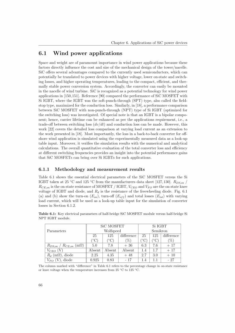
Chapter 6. Applications of SiC power devices
6.1 Wind power applications
Space and weight are of paramount importance in wind power applications because thesefactors directly influence the cost and size of the mechanical design of the tower/nacelle.SiC offers several advantages compared to the currently used semiconductors, which canpotentially be translated to power devices with higher voltage, lower on-state and switch-ing losses, and higher operating temperatures, leading to the compact, efficient, and ther-mally stable power conversion system. Accordingly, the converter can easily be mountedin the nacelle of wind turbine. SiC is recognized as a potential technology for wind powerapplications in [150,151]. Reference [90] compared the performance of SiC MOSFET withSi IGBT, where the IGBT was the soft-punch-through (SPT) type, also called the field-stop type, maximized for the conduction loss. Similarly, in [18], a performance comparisonbetween SiC MOSFET with non-punch-through (NPT) type of Si IGBT (optimized forthe switching loss) was investigated. Of special note is that an IGBT is a bipolar compo-nent; hence, carrier lifetime can be enhanced as per the applications requirement, i.e., atrade-off between switching loss (dv/dt) and conduction loss can be made. However, thiswork [22] covers the detailed loss comparison at varying load current as an extension tothe work presented in [18]. Most importantly, the loss in a back-to-back converter for off-shore wind application is simulated using the experimentally measured data as a look-uptable input. Moreover, it verifies the simulation results with the numerical and analyticalcalculations. The overall quantitative evaluation of the total converter loss and efficiencyat different switching frequencies provides an insight into the potential performance gainsthat SiC MOSFETs can bring over Si IGBTs for such applications.
6.1.1 Methodology and measurement results
Table 6.1 shows the essential electrical parameters of the SiC MOSFET versus the SiIGBT taken at 25 C and 125 C from the manufacturers data sheet [127,130]. RDS,on /RCE,on is the on-state resistance of MOSFET / IGBT, VCEO and VFO are the on-state kneevoltage of IGBT and diode, and Rd is the resistance of the freewheeling diode. Fig. 6.1(a) and (b) show the turn-on (Eon), turn-off (Eoff ) and total losses (Etot) with varyingload current, which will be used as a look-up table input for the simulation of converterlosses in Section 6.1.2.
Table 6.1: Key electrical parameters of half-bridge SiC MOSFET module versus half-bridge SiNPT IGBT module.
ParametersSiC MOSFET Si IGBT
Wolfspeed Semikron25 125 difference 25 125 difference
(C) (C) (%) (C) (C) (%)RDS,on / RCE,on (mΩ) 5.0 7.8 + 36 6.3 7.6 + 17VCEO (V) Absent Absent Absent 1.4 1.7 + 17Rd (mΩ), diode 2.25 4.35 + 48 2.7 3.0 + 10VFO (V), diode 0.925 0.83 - 17 1.4 1.1 - 27
The column marked with “difference” in Table 6.1 refers to the percentage change in on-state resistanceor knee voltage when the temperature increases from 25 C to 125 C.
66

Chapter 6. Applications of SiC power devices
0 60 120 180 240 300Load current [A]
0
3
6
9
12
15
18
Ene
rgy
loss
[m
J]
(a) Switching energy loss of SiC MOSFET.
0 60 120 180 240 300Load current [A]
0
5
10
15
20
25
30
35
Ene
rgy
loss
[m
J]
(b) Switching energy loss of Si IGBT.
Figure 6.1: Plot of Eon, Eoff , and Etot of SiC MOSFET (a) and Si IGBT (b) at VDC of 600 V.
6.1.2 Topology selection and simulation of losses
Primarily, there are two main popular and commercialized voltage source converter (VSC)topologies in offshore wind applications. The first is a three-phase, two-level type and thesecond is a three-phase, three-level neutral point diode clamped (3L-NPC) type [152,153].The former topology is employed for the low-voltage and the latter for the high-voltageapplications. These converters are mounted in a back-to-back configuration such thateach shares the same DC-link as illustrated in Fig. 6.2. One converter acts as a rectifier(connected on the generator side) and another converter acts as an inverter (connectedon the grid side). When IGBTs/MOSFETs along with anti-parallel diodes are used, theconverter allows for a bidirectional flow of power. In this work, a three-phase, two-leveltopology, as shown in Fig. 6.2, is chosen where the main purpose is to study the powerlosses in the back-to-back converter and perform the comparison between all-Si and all-SiC devices. Using MATLAB Simulink, the switching loss obtained from the laboratorymeasurements and the conduction loss from the data sheet are used as a look-up tableor polynomial functions based on the curve fitting for simulating the total converter loss.The loss is simulated for a space vector PWM (SVPWM) [154], DC-link voltage (VDC) of760 V, modulation index (m) of 1, and a load current (Iout,rms) of 300 A. The converteroutput voltage (Vout,rms) is about 460 V (
√3/(2 ·
√2) · VDC · m) and the power rating is
approximately 240 kW.
LC Filter
LC Filter
Grid
Step-up Transformer
Synchronous Generator
Generator Rectifier Grid Inverter
DC-Link 760 V
AB
CT1 D1
IT1 ID1
460 V AC 460 V AC
Turbine
VAB
Iout
Figure 6.2: Schematic diagram of a two-level, three-phase, back-to-back converter configurationfor low-voltage offshore wind applications. Current in one of the top switches and diodes of grid-side inverter are denoted by IT1 and ID1, correspondingly.
67

Chapter 6. Applications of SiC power devices
0.45 0.46 0.47 0.48 0.49 0.5-500
0
500Output current, I
out [A]
0.45 0.46 0.47 0.48 0.49 0.5-1000
0
1000Voltage between terminal A and B, V
AB [V]
0.45 0.46 0.47 0.48 0.49 0.5-1
0
1Switching signal to IGBT T1, m = 1, cos = 1
0.45 0.46 0.47 0.48 0.49 0.50
500Switching current in diode D1, I
D1 [A]
0.45 0.46 0.47 0.48 0.49 0.50
500Switching current in IGBT T1, I
T1 [A]
0.45 0.46 0.47 0.48 0.49 0.50
4
8104 Instantaneous power loss of IGBT T1 [W]
0.45 0.46 0.47 0.48 0.49 0.5
time [s]
0
400
800Average power loss of IGBT T1 [W] with 0.01 s filter
Figure 6.3: Illustration of the sample of simulated waveforms at various points in the schematicfor the grid-side inverter in a standard two-level topology. With the DC-link voltage of 760 V,RMS output current of 300 A, cosφ of unity, modulation index of 1, and switching frequencyof 600 Hz, the total simulated power loss of IGBT T1 is 433 W, the instantaneous and averagepower losses are displayed in the lower two graphs.
6.1.3 Simulation results
Fig. 6.3 illustrates the simulated waveforms of the inverter-side, such as output current(Iout), voltage between terminals A and B (VAB), switching signal to IGBT T1, switchingcurrent in diode D1 (ID1), switching current in IGBT T1 (IT1), instantaneous power loss of
68

Chapter 6. Applications of SiC power devices
IGBT T1, and average power loss of IGBT T1 with a filter of 0.01 (1/60) s. These sampleplots are exemplified with switching frequency (fsw) of 600 Hz, fundamental frequency of60 Hz and m of 1. Note that the reasons for selecting fsw of 600 Hz are: lower fsw meansfew switching events and thereby better visibility, and eases the calculation during theverification phase in the following section.
6.1.3.1 Numerical verification of the simulation results
In the numerical verification method, the turn-on, turn-off, and total switching powerlosses of IGBT T1; Psw−on−T1, Psw−off−T1, and Psw−tot−T1, correspondingly; are com-puted by counting the number of switching events during the fundamental cycle of theoutput. Table 6.2 lists the reading of currents and the corresponding energy losses fromFig. 6.4 (a) and (b), respectively. Note that Fig. 6.4 (b) is derived from Fig. 6.1 (b) byextrapolation of data from 300 A to 450 A using the same coefficients of polynomial asobtained by curve fitting the plot from 30 A to 300 A. The total sum of Eon is 133.3 mJ(11.8 + 34 + 50 + 31 + 6.49 = 133.3 mJ), and as a result Psw−on−T1 of IGBT T1 is10.13 W (133.3/1000 × 760/600 × 60 = 10.13 W). Similarly, the total sum of Eoff is38.19 mJ and Psw−off−T1 is 2.90 W, and thus, Psw−tot−T1 is 13.03 W, as listed in Table 6.3in the row named “Numerical”. As the percentage differences between numerically calcu-lated and simulated losses with reference to the numerical losses are below 4%, as shownin Table 6.3, indicated by row “Error”, the simulation results have reasonable accuracy.
Table 6.2: Reading of currents and energy losses (refer Fig. 6.4 (a) and (b).
IT1 [A] 90 160 340 350 425Eon[mJ] 11.8 34 50 31 6.49Eoff [mJ] 1.59 10 12.8 10.4 3.4
0.016 0.018 0.02 0.022 0.024 0.026time [s]
0
50
100
150
200
250
300
350
400
450
I T1 [
A]
OnOff
(a) Switching current in IGBT T1.
0 60 120 180 240 300 360 420 480Load current [A]
0
10
20
30
40
50
60
Ene
rgy
loss
[m
J]
(b) Fig. 6.1 (b) is extrapolated upto 450 A.
Figure 6.4: (a) Detailed (zoomed in) view of switching current in IGBT T1. The RMS outputcurrent is 300 A, m is 1, cosφ is 1, fundamental frequency is 60 Hz, and switching frequency is600 Hz. (b) Extrapolation of Fig. 6.1 (b) to fill in values in Table 6.2.
69

Chapter 6. Applications of SiC power devices
Table 6.3: A comparison of simulated and numerically calculated power loss of transistor T1.
Power loss [W] Psw−on−T1 Psw−off−T1 Psw−tot−T1
Simulation 9.75 2.79 12.55Numerical 10.13 2.90 13.03Error [%] 3.75 3.79 3.68
The variables used in Table 6.3 are: turn-on, turn-off, and total switching power losses of IGBT T1;Psw−on−T1, Psw−off−T1, and Psw−tot−T1, respectively.
6.1.3.2 Analytical verification of the simulation results
The switching loss of IGBT/MOSFET (Psw−trans−T1) can be estimated using analyticalapproximations as long as the energy loss during switching is linearly dependent on thecollector current, as given by (6.1) [155]. Compared to the simulated results, as presentedin Table 6.3, the error was found to be in the range of 5–10%. This is essentially dueto the assumption of linear dependence in (6.1) during analytical calculations, whereasswitching loss is taken as a quadratic function of current during simulations. Moreover,considering the sinusoidal dependency of duty cycles versus time, the on-state power lossof IGBT (Pcond−trans−T1) and diode (Pcond−diode−D1) can be calculated by using (6.2) and(6.3), respectively [156,157].
Psw−trans−T1 = fsw · (Eon + Eoff ) ·√
2
π· Iout,rms
Iref· VDC
Vref(6.1)
Pcond−trans−T1 = VCEO · Iout ·(
1
2 · π± m · cosφ
8
)+RCE,on · I2out ·
(1
8± m · cosφ
3 · π
)(6.2)
Pcond−diode−D1 = VFO · Iout ·(
1
2 · π∓ m · cosφ
8
)+Rd · I2out ·
(1
8∓ m · cosφ
3 · π
)(6.3)
In these equations where ± are present, the upper sign applies for an inverter mode(motor operation) and the lower sign for a rectifier mode (generator operation). For aMOSFET, the first term in (6.2) will be zero because it does not possess knee voltage. Forthe greater clarity, a description of symbols used in (6.1)–(6.3) is provided in Table 6.4.Note that φ is a phase angle of current with respect to voltage, which is -90 ≤ +90
for an inverter or a motor operation, and +90 ≤ +270 for rectifier or generator mode.However, the worst cases: 0 for motor, and 180 for generator, are analyzed in this work.The differences in analytically calculated and simulated conduction losses with respect tothose with analytically calculated alone are found to be below 3%.
Table 6.4: Definition of symbols used in (6.1) - (6.3).
Symbol Description ValueVref reference voltage 600 VIref reference current 300 Aφ phase angle between current and voltage 0 (inverter), 180 (rectifier)
Iout peak output current√
2 × Iout,rms = 424 Afsw switching frequency 1 kHz - 50 kHzm modulation index 1
70

Chapter 6. Applications of SiC power devices
6.1.4 Evaluation of inverter power loss at different switchingfrequencies
A detailed loss breakdown at various switching frequencies (1 to 50 kHz) is provided inFig. 6.5. The chosen IGBT is a NPT type optimized for the fast switching over theconduction loss. Simulation results show that the conduction loss in the Si IGBT inverteris higher by a factor of 2 at 25 C to that in the SiC MOSFET inverter. Furthermore, theresults showed that the total conduction loss (Pcond−trans) is approximately equal to thetotal switching loss (Psw−trans) at around 15 and 25 kHz for the all-Si and all-SiC inverters,accordingly, i.e., for the low frequency region, the conduction loss is a dominating partof the total inverter loss. It should be pointed out that the turn-off power losses of theselected devices are almost equal because the NPT IGBT switches off as fast as SiCMOSFET. The all-Si inverter has approximately 3.3 times higher Psw−trans than that ofthe all-SiC inverter, the major share being the combined loss of Psw−on−trans and Prr.Therefore, in order to use Si IGBT at higher switching frequency, a practical solutionwould be the use of a SiC diode as an anti-parallel diode instead of Si diode (a Hybridsolution) as this solution leads to the reduction in Prr, and subsequently its influence onPsw−on−trans. Nonetheless, SiC MOSFET is a better solution than NPT IGBT for all therange of switching frequencies, unlike in a SPT IGBT, as discussed in the previous work,where the losses were comparable for lower frequencies (≤ 3 kHz) [90].
1 2 3 4 5 6 7 8 9 10 20 30 40 50Switching frequency [kHz]
0123456789
101112
Pow
er lo
ss [
kW]
Figure 6.5: Breakdown of power loss in an inverter at different switching frequencies. Thelegends in the bar chart are: turn-on switching loss (Psw−on−trans), turn-off switching loss(Psw−off−trans), diode recovery loss (Prr), conduction loss in a transistor (Pcond−trans), andconduction loss in a diode (Pcond−diode). SiC MOSFET helps to reduce the switching loss, whichis a dominant part of the total loss in an IGBT inverter, particularly the Psw−on−trans. Inverterswith SiC MOSFET can switch at higher frequency compared to those with Si IGBT with almostthe same total power loss: an example of which is indicated in the bar chart where the frequencyis about six times higher in SiC than in Si for the same total inverter power loss of about 4 kW.
71

Chapter 6. Applications of SiC power devices
6.1.5 Evaluation of back-to-back converter efficiency at differentswitching frequencies
A comparison of the total converter efficiency in a back-to-back converter using the all-SiC devices with the all-Si devices is depicted in Fig. 6.6. The converter with the SiCMOSFET shows 0.86 and 5.04% higher efficiencies at 1 and 50 kHz, correspondingly overtheir Si IGBT counterparts, as depicted in Fig. 6.6. The simulated switching losses of theback-to-back converters are equal, but the conduction losses are not. For instance, in thecase of a rectifier mode, the simulated Pcond−trans is lower and Pcond−diode is higher by afactor of 10 compared to those, correspondingly, in the case of an inverter mode.
Hence, the SiC MOSFET offers lower on-state and switching losses compared to SiIGBT. Moreover, the MOSFET structure possesses an intrinsic diode with a switchingperformance that is almost like a SiC Schottky diode, and thereby, the need for an addi-tional anti-parallel diode can be eliminated. However, there is no such possibility in IGBTstructure. The VSC with high-voltage SiC MOSFETs (when available in ≈ 10 kV range)will be the most attractive candidate for high-voltage direct current (HVDC) connectionsto offshore wind-farms as efficiency becomes more important.
0 5 10 15 20 25 30 35 40 45 50Switching frequency [kHz]
90919293949596979899
100
Eff
icie
ncy
[%]
Figure 6.6: Comparison of SiC MOSFET and Si IGBT efficiencies in a three-phase back-to-backconverter illustrates that at all the switching frequencies, the higher efficiency SiC MOSFETsprovide a performance advantage over their Si IGBT counterparts. At switching frequencies of1 kHz, 3 kHz (practical for today’s offshore applications) and 50 kHz, converter with the SiCMOSFET shows 0.86%, 1.05% and 5.04% higher efficiencies over Si IGBT.
6.1.6 Discussion and summary
This section discusses the conduction and switching losses in two different sets of MOS-FETs and IGBTs during motoring and generating modes.
6.1.6.1 Six-pack, SiC MOSFET and Si SPT IGBT
Table 6.5 lists the central parameters of six-pack SiC MOSFET versus six-pack Si IGBTmodules required for computing conduction losses. Table 6.6 summarizes the conduc-tion losses in a two-level VSC during motoring and generating modes. As mentioned in
72

Chapter 6. Applications of SiC power devices
Chapter 4, this Si IGBT is called an SPT type, where the conduction losses are opti-mized over switching losses. The additional variables used in Table 6.6 are: Pcond−tot andPcond−norm−SiC , which correspond to total conduction loss and normalized total conduc-tion loss with regard to the total conduction loss of SiC devices. As seen in Table 6.5,the on-state resistances show a positive temperature coefficient, while the opposite is trueconcerning the knee-voltages. In all-Si solutions, the aggregate conduction losses are lowerduring both the motoring and the generating modes compared to those in all-SiC solu-tions at 125 C, as evident from Table 6.6. Moreover, these losses are higher by just afactor of 1.14 in all-Si compared to all-SiC solutions at 25 C. In [90], these sets of devicesare evaluated and it is illustrated that a converter solution with SiC MOSFET is moreefficient throughout the whole switching frequency range: 1 to 100 kHz, compared to thesolution with Si IGBT.
Table 6.5: Key electrical parameters of the six-pack SiC MOSFET module versus the six-packSi SPT IGBT module.
ParametersCCS050M12CM2 FS75R12KT4 B15
Wolfspeed Infineon25 125 difference 25 125 difference
(C) (C) (%) (C) (C) (%)RDS,on / RCE,on (mΩ) 8.33 13.13 + 57.6 3.7 5.17 + 39.7VCEO (V) Absent Absent Absent 1 0.84 - 16Rd (mΩ), diode 3.33 6.59 + 97.7 3.15 3.54 + 12.2VFO (V), diode 0.85 0.77 - 9.4 1.05 0.93 - 11.4
Table 6.6: Conduction losses of SiC MOSFET versus Si IGBT modules (six-packs) in a two-level VSC during motoring versus generating operations at two different junction temperatures.
Motoring Generating
ParametersSiC MOSFET Si IGBT SiC MOSFET Si IGBT
Wolfspeed Infineon Wolfspeed InfineonTj (C) 25 125 25 125 25 125 25 125Pcond−trans (W) 520 819 593 626 43 67 62 63Pcond−diode (W) 54 67 62 58 515 689 577 557Pcond−tot (W) 574 886 655 684 558 756 639 620Pcond−norm−SiC 1 1 1.14 0.77 1 1 1.14 0.82
6.1.6.2 Half-bridge, SiC MOSFET and Si NPT IGBT
Table 6.7 summarizes the similar results with another sets of SiC MOSFET and Si IGBT.Here the IGBT is a PT type and is optimized for high speed switching over conductionlosses. Looking back in Chapter 4, at similar dv/dt of 5 V/ns, the Eoff losses are roughlythe same in these sets of devices; however, the conduction losses, as listed in Table 6.7, aresignificantly higher in Si IGBT compared to those in SiC MOSFET, particularly duringmotoring mode.
73

Chapter 6. Applications of SiC power devices
Table 6.7: Conduction losses of SiC MOSFET versus Si IGBT modules (half-bridges) in a two-level VSC during motoring versus generating operations at two different junction temperatures.
Motoring Generating
ParametersSiC MOSFET Si IGBT SiC MOSFET Si IGBT
Wolfspeed Semikron Wolfspeed SemikronTj (C) 25 125 25 125 25 125 25 125Pcond−trans (W) 1248 1947 2585 3122 102 159 250 302Pcond−diode (W) 126 161 177 157 1230 1683 1687 1545Pcond−tot (W) 1374 2107 2762 3280 1332 1842 1937 1848Pcond−norm−SiC 1 1 2 1.55 1 1 1.45 1.0
6.1.6.3 Low speed and high speed drives
In low speed motor drive applications, the fundamental frequency of motor is 50/60 Hz.Thus, the motor is heavy and large, as a consequence, the inductance of motor worksas a filter. In such an application, dv/dt is limited between 2 V/ns to 5 V/ns to keepinsulation of motor winding safe, the solution with SiC MOSFETs can be considered intwo ways. The first is to switch them as slowly as Si IGBTs and thereby benefit fromtheir low conduction losses. The second is to switch them to their fast switching potential,but keep the switching frequency low like today (< 5 kHz). This way, these converterscan benefit from both switching and conduction losses, and thus the size of heat sinkcan be substantially reduced. However, if this is the case, there will be losses in thedv/dt filter. Therefore, the question is whether the losses should be in the active devices(MOSFET/IGBT) by slowing down devices via a gate driver to satisfy dv/dt limits or ifthe losses should be in the dv/dt filter. Note that dv/dt filter is L-RC-L (L is inductor,R is resistor and C is capacitor) type, as there will be losses in R, cooling is required.Therefore, it would be interesting to carry out research regarding the optimal losses withthese solutions, but it is not within the scope of this thesis.
In high speed motor drive applications, the fundamental frequency of motor is con-siderably higher. For instance, in aircraft, it is ≥ 400 Hz. Higher frequency enables morepower for the same motor volume and mass. Moreover, space and weight are predom-inant in such applications, and thus transformer and motor sizes can be reduced withhigh-frequency switching. As a consequence, the fuel consumption is reduced. SiC offerslow switching losses, its characteristics remain almost unaffected by high temperatures,and heat can be readily extracted from the device, resulting in smaller cooling require-ments and hence smaller and lighter converter.
6.2 Induction heating applications
High-frequency is the main driving force for induction heating applications, especially forthe surface heating of relatively small parts or tubes with small diameters, where only athin layer of the surface should be hardened or welded. In the 1.2–1.7 kV voltage class,Si-based power devices, particularly Si IGBTs, have been the primary choice for powerelectronic devices for the last several decades. In fact, Si MOSFETs exhibit high on-statelosses in this voltage class, impeding them from being commercially available. Typically,the highest operating frequency of the state-of-the-art Si IGBTs for soft switched appli-
74
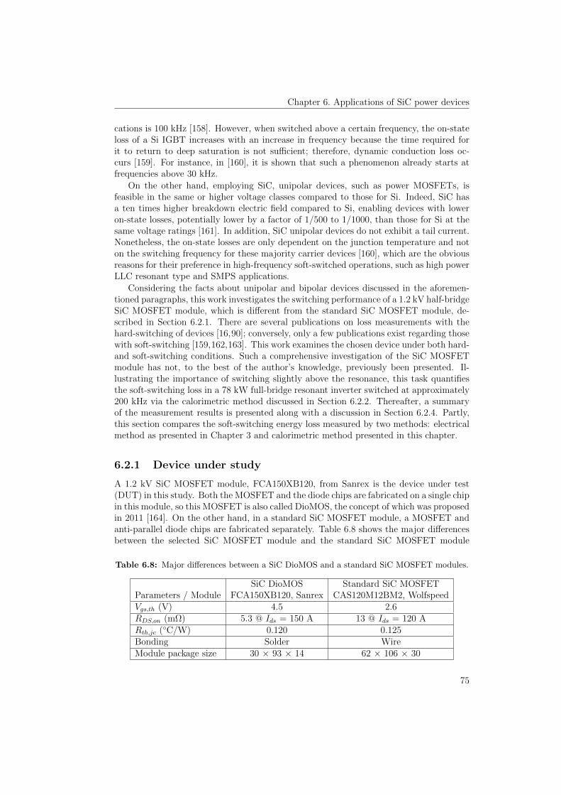
Chapter 6. Applications of SiC power devices
cations is 100 kHz [158]. However, when switched above a certain frequency, the on-stateloss of a Si IGBT increases with an increase in frequency because the time required forit to return to deep saturation is not sufficient; therefore, dynamic conduction loss oc-curs [159]. For instance, in [160], it is shown that such a phenomenon already starts atfrequencies above 30 kHz.
On the other hand, employing SiC, unipolar devices, such as power MOSFETs, isfeasible in the same or higher voltage classes compared to those for Si. Indeed, SiC hasa ten times higher breakdown electric field compared to Si, enabling devices with loweron-state losses, potentially lower by a factor of 1/500 to 1/1000, than those for Si at thesame voltage ratings [161]. In addition, SiC unipolar devices do not exhibit a tail current.Nonetheless, the on-state losses are only dependent on the junction temperature and noton the switching frequency for these majority carrier devices [160], which are the obviousreasons for their preference in high-frequency soft-switched operations, such as high powerLLC resonant type and SMPS applications.
Considering the facts about unipolar and bipolar devices discussed in the aforemen-tioned paragraphs, this work investigates the switching performance of a 1.2 kV half-bridgeSiC MOSFET module, which is different from the standard SiC MOSFET module, de-scribed in Section 6.2.1. There are several publications on loss measurements with thehard-switching of devices [16,90]; conversely, only a few publications exist regarding thosewith soft-switching [159,162,163]. This work examines the chosen device under both hard-and soft-switching conditions. Such a comprehensive investigation of the SiC MOSFETmodule has not, to the best of the author’s knowledge, previously been presented. Il-lustrating the importance of switching slightly above the resonance, this task quantifiesthe soft-switching loss in a 78 kW full-bridge resonant inverter switched at approximately200 kHz via the calorimetric method discussed in Section 6.2.2. Thereafter, a summaryof the measurement results is presented along with a discussion in Section 6.2.4. Partly,this section compares the soft-switching energy loss measured by two methods: electricalmethod as presented in Chapter 3 and calorimetric method presented in this chapter.
6.2.1 Device under study
A 1.2 kV SiC MOSFET module, FCA150XB120, from Sanrex is the device under test(DUT) in this study. Both the MOSFET and the diode chips are fabricated on a single chipin this module, so this MOSFET is also called DioMOS, the concept of which was proposedin 2011 [164]. On the other hand, in a standard SiC MOSFET module, a MOSFET andanti-parallel diode chips are fabricated separately. Table 6.8 shows the major differencesbetween the selected SiC MOSFET module and the standard SiC MOSFET module
Table 6.8: Major differences between a SiC DioMOS and a standard SiC MOSFET modules.
SiC DioMOS Standard SiC MOSFETParameters / Module FCA150XB120, Sanrex CAS120M12BM2, WolfspeedVgs,th (V) 4.5 2.6RDS,on (mΩ) 5.3 @ Ids = 150 A 13 @ Ids = 120 ARth,jc (C/W) 0.120 0.125Bonding Solder WireModule package size 30 × 93 × 14 62 × 106 × 30
75
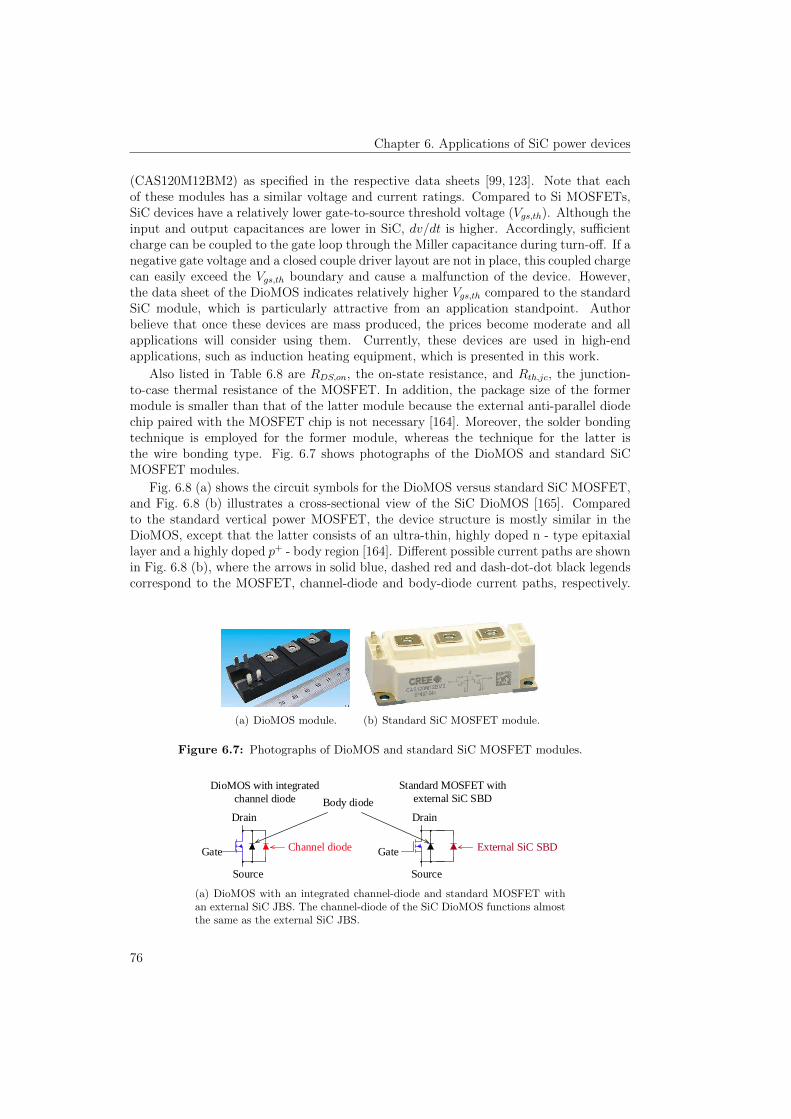
Chapter 6. Applications of SiC power devices
(CAS120M12BM2) as specified in the respective data sheets [99, 123]. Note that eachof these modules has a similar voltage and current ratings. Compared to Si MOSFETs,SiC devices have a relatively lower gate-to-source threshold voltage (Vgs,th). Although theinput and output capacitances are lower in SiC, dv/dt is higher. Accordingly, sufficientcharge can be coupled to the gate loop through the Miller capacitance during turn-off. If anegative gate voltage and a closed couple driver layout are not in place, this coupled chargecan easily exceed the Vgs,th boundary and cause a malfunction of the device. However,the data sheet of the DioMOS indicates relatively higher Vgs,th compared to the standardSiC module, which is particularly attractive from an application standpoint. Authorbelieve that once these devices are mass produced, the prices become moderate and allapplications will consider using them. Currently, these devices are used in high-endapplications, such as induction heating equipment, which is presented in this work.
Also listed in Table 6.8 are RDS,on, the on-state resistance, and Rth,jc, the junction-to-case thermal resistance of the MOSFET. In addition, the package size of the formermodule is smaller than that of the latter module because the external anti-parallel diodechip paired with the MOSFET chip is not necessary [164]. Moreover, the solder bondingtechnique is employed for the former module, whereas the technique for the latter isthe wire bonding type. Fig. 6.7 shows photographs of the DioMOS and standard SiCMOSFET modules.
Fig. 6.8 (a) shows the circuit symbols for the DioMOS versus standard SiC MOSFET,and Fig. 6.8 (b) illustrates a cross-sectional view of the SiC DioMOS [165]. Comparedto the standard vertical power MOSFET, the device structure is mostly similar in theDioMOS, except that the latter consists of an ultra-thin, highly doped n - type epitaxiallayer and a highly doped p+ - body region [164]. Different possible current paths are shownin Fig. 6.8 (b), where the arrows in solid blue, dashed red and dash-dot-dot black legendscorrespond to the MOSFET, channel-diode and body-diode current paths, respectively.
(a) DioMOS module. (b) Standard SiC MOSFET module.
Figure 6.7: Photographs of DioMOS and standard SiC MOSFET modules.
Gate
Body diode
Channel diode
Drain
Source
External SiC SBD
Drain
Source
Gate
DioMOS with integrated
channel diode
Standard MOSFET with
external SiC SBD
(a) DioMOS with an integrated channel-diode and standard MOSFET withan external SiC JBS. The channel-diode of the SiC DioMOS functions almostthe same as the external SiC JBS.
76
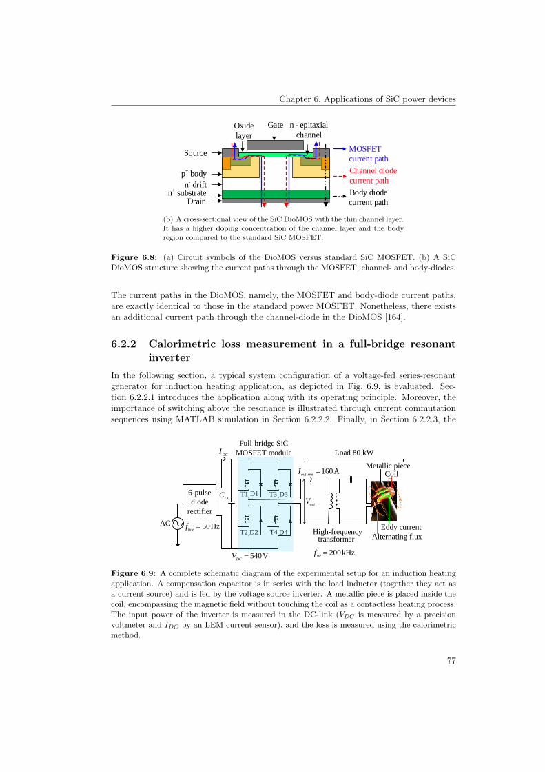
Chapter 6. Applications of SiC power devices
Drain
Source
GateOxide
layer
n - epitaxial
channel
Body diode
current path
Channel diode
current path
MOSFET
current path
p+ body
n- driftn+ substrate
(b) A cross-sectional view of the SiC DioMOS with the thin channel layer.It has a higher doping concentration of the channel layer and the bodyregion compared to the standard SiC MOSFET.
Figure 6.8: (a) Circuit symbols of the DioMOS versus standard SiC MOSFET. (b) A SiCDioMOS structure showing the current paths through the MOSFET, channel- and body-diodes.
The current paths in the DioMOS, namely, the MOSFET and body-diode current paths,are exactly identical to those in the standard power MOSFET. Nonetheless, there existsan additional current path through the channel-diode in the DioMOS [164].
6.2.2 Calorimetric loss measurement in a full-bridge resonantinverter
In the following section, a typical system configuration of a voltage-fed series-resonantgenerator for induction heating application, as depicted in Fig. 6.9, is evaluated. Sec-tion 6.2.2.1 introduces the application along with its operating principle. Moreover, theimportance of switching above the resonance is illustrated through current commutationsequences using MATLAB simulation in Section 6.2.2.2. Finally, in Section 6.2.2.3, the
Full-bridge SiC
MOSFET module
transformerT4
T3
T2
T16-pulse
diode
rectifier
High-frequency AC
D1
D2
D3
D4
outV
DCC
Metallic pieceCoil
Alternating flux
Eddy current
540VDC
V
DCI
50Hzline
f
200kHzsw
f
,160A
out rmsI
Load 80 kW
Figure 6.9: A complete schematic diagram of the experimental setup for an induction heatingapplication. A compensation capacitor is in series with the load inductor (together they act asa current source) and is fed by the voltage source inverter. A metallic piece is placed inside thecoil, encompassing the magnetic field without touching the coil as a contactless heating process.The input power of the inverter is measured in the DC-link (VDC is measured by a precisionvoltmeter and IDC by an LEM current sensor), and the loss is measured using the calorimetricmethod.
77

Chapter 6. Applications of SiC power devices
calorimetric loss measurement of the inverter part is presented to find the merits of usingSiC MOSFETs for such an application.
6.2.2.1 System configuration and working principle
Before delving into the working principle of induction heating welders, it is important todiscuss the system configuration considered in this study. As seen in Fig. 6.9, the voltagesource inverter consists of two half-bridge SiC MOSFET modules with anti-parallel diodes,the DC power for which is fed through a six-pulse diode rectifier connected to a 400 V,50 Hz power supply. The abbreviations used in the schematic are as follows. IDC : DC-link current, VDC : DC-link voltage, Vout: output voltage and Iout: output current. Theload is composed of a compensating capacitor, a heating coil, and a metallic piece tobe welded. Essentially, when the coil is subjected to a high-frequency sinusoidal currentgenerated from the inverter, a time-varying magnetic field is induced in it. Consequently,the metal piece is heated by two physical phenomenons, eddy currents and magnetichysteresis. Eddy currents oppose the magnetic field the work piece is subjected to andproduces heating via the Joule effect, and this is the primary heat source. Furthermore,the magnetic field causes dipoles of the ferromagnetic material to oscillate when thepoles change their polar orientation every cycle, thus creating additional heat due tofriction, referred to as hysteresis loss. Depending on the application, the AC frequencyis controlled to regulate the penetration depth into the work piece. SiC MOSFETs havepotential to switch extremely fast and are very promising components for next-generationhigh-frequency induction heating generators. By utilizing the benefits of the skin effect,these generators can be used for surface heating of relatively small parts or tubes withsmall diameters, where only a thin layer of the surface should be hardened or welded.
6.2.2.2 Inductive (fsw > fres) versus capacitive (fsw < fres) mode switching -Consequence in terms of loss
When an inverter is switched at resonant frequency (fres), the maximum power can betransferred. Nevertheless, the real-world system has a very low chance to operating atperfect resonance because the focal point can shift due to small changes in the load orsubtle inaccuracies in the control parameters. As a consequence, in normal operation, theinverter works slightly above or below the resonance. Therefore, this section aims to studythe sequence of the commutation process during the inductive (above resonance) versuscapacitive (below resonance) switching modes. Thus, the full-bridge inverter configura-
T4
T3
T2
T1
14T
I
14T
I
D1
D2
D3
D4
outV
DCC
T4
T3
T2
T1
23D
I
23D
I
D1
D2
D3
D4
outV
DCC
DCV
DCV
outI
outI
Figure 6.10: Exemplification of the current flow during the positive polarity of the load current.
78

Chapter 6. Applications of SiC power devices
tion, shown in Fig. 6.9, is simulated in MATLAB. The inputs for simulation are as follows:VDC = 540 V, the resistance of the metallic piece is chosen such that Iout,rms = 160 A, andthe inductance of the coil and compensating capacitance are tuned to acquire the desiredfres. Fig. 6.10 shows the current flow during the positive polarity of the load current,where the current through transistors T1 and T4 is labelled as IT14+ and that throughD2 and D3 is depicted as ID23+ . In a similar manner, IT23− and ID14− are the currents inthe respective transistors and diodes during the negative polarity of the load current, assymbolized in the simulated waveforms presented in Fig. 6.11.
The plots show that while operating above the resonance, Fig. 6.11 (a), diode turn-on and switch turn-off feature hard-switching, while diode turn-off and switch turn-onexhibit soft-switching. While operating under the resonance, Fig. 6.11 (b), on the otherhand, the converse of the former sequences holds true. The forward-recovery of the diodeis significantly smaller compared to the reverse-recovery, so switching slightly above theresonance is preferable (to avoid turn-off losses associated with the diodes), and thisapproach is adopted in this work.
1.99 1.992 1.994 1.996 1.998 2
10-3
-2000
200400600
1.99 1.992 1.994 1.996 1.998 2
10-3
-600-400-200
0200
1.99 1.992 1.994 1.996 1.998 2time [s] 10-3
-1000
0
1000
(a) Inductive mode switching, fsw > fres.
1.99 1.992 1.994 1.996 1.998 2
10-3
-2000
200400600
1.99 1.992 1.994 1.996 1.998 2
10-3
-600-400-200
0200
1.99 1.992 1.994 1.996 1.998 2time [s] 10-3
-1000
0
1000
(b) Capacitive mode switching, fsw < fres
Figure 6.11: Illustration of inductive and capacitive switching modes in a series-resonantinverter. In the former mode, the turn-on of diodes and turn-off of switches are hard, but theturn-off of diodes and turn-on of switches are soft. However, the converse is true in the lattermode, leading to a higher switching loss, particularly that from the reverse-recovery of diodes.This is why the former mode is adopted in this work over the latter.
6.2.2.3 Laboratory measurements
First, it is essential to highlight that a low-inductive switching loop is the key factorfor utilizing the fast switching potential of a SiC MOSFET and maintaining the safety,particularly during failure. Hence, a DC-link busbar is constructed with a stripline-terminated capacitor, as depicted in Fig. 6.12. The switching frequency is 187 kHz (forthis case), and the inverter losses are measured calorimetrically at approximately 78 kWof input power. Fig. 6.13 displays the oscilloscope waveforms with the output voltage
79

Chapter 6. Applications of SiC power devices
DC-link capacitor
Gate driver
Heat sink with water cooling
inpT out
T
Sanrex SiC modules
Figure 6.12: Part of the experimental setup showing a low-inductive busbar connection for afull-bridge inverter with a water-cooled heat sink for calorimetric loss measurement.
,160A
out rmsI
540Vout
V
187sw
f kHz
Figure 6.13: Illustration of a sample of inverter output voltage and current with a full PWMcontrol scheme. The gate voltage is + 20 V / - 5 V, and the gate resistance is 2.85 Ω.
and current. In the calorimetric method, the inverter is placed over the water-cooledheat sink, assuming that all the heat dissipated by the inverter is removed through thecooling system. When switched just above the resonance, the turn-on loss is absent(details explained in Section 6.2.2.2), thus the total loss comprises the turn-off switchingloss and conduction loss. Thereafter, by subtracting the conduction loss from the totalloss, the turn-off loss is computed. Various electrical parameters, namely, IDC , VDC , andIout,rms, thermal parameters, namely, the inlet and outlet water temperatures (Tinp andTout, respectively), and the water mass (m) are monitored and listed in Table 6.9.
Table 6.9: Summary of the measured parameters at 78 kW input power.
Measured parameters IDC (A) VDC Iout,rms Tinp Tout m
(A) (V) (A) (C) (C) (g/min)
Values 142.8 545 160.3 15 17.5 2.990
80

Chapter 6. Applications of SiC power devices
Table 6.10 presents a summary of the calculated parameters. Using (7.4)–(7.10), thecorresponding parameters in each row are computed. The abbreviations used in the equa-tions are as follows: Pinp: input power of the inverter, Q: total power loss of the inverter,s: specific heat capacity of water (4.186 J/g/C), η: efficiency of the inverter, Pcond:conduction power loss per switch, Psw: switching power loss per switch, Eoff−spec−calori:specific turn-off energy loss per switch, and ∆T: temperature rise from the junction to thecase. The measured efficiency of the inverter is approximately 99.33%, the conduction lossper switch is 89.93 W with RDS,on being 7 mΩ (at the operating temperature), and thetemperature rise is 15.64 C (at the given Rth,jc of 0.120 C/W). It is worth mentioningthat Eoff−spec−calori is computed for a drain-source current of 60 A, which is the turn-offswitching current in a full-bridge.
Table 6.10: Summary of the calculated parameters for approximately 78 kW of input power.
Calculated parameters Values Equations Eq. no.
Pinp (kW) 77.82 Pinp = VDC · IDC (7.4)
Q (W or J/s) 521.5 Q = m · s · (Tout − Tinp) (7.5)
η (%) 99.33 η =Pinp −QPinp
(7.6)
Pcond (W) 89.93 Pcond =
(Iout√
2
)2
·RDS,on (7.7)
Psw (W) 40.44 Psw =Q
4− Pcond (7.8)
Eoff−spec−calori (µJ/A) 3.60 Eoff−spec−calori =Psw
fsw · Ids(7.9)
∆T (C) 15.64 ∆T = Rth,jc ·Q
4(7.10)
6.2.3 Accuracy analysis of calorimetric efficiency measurement
As ∆T and m in (7.5) can be the sources of inaccuracies in the calorimetric loss measure-ment method, the inlet and outlet temperatures are measured using an analog thermome-ter with ± 0.05 C accuracy. For the water flow measurement, first, the outlet wateris run into a bucket over a specified time (2 minutes), second, the water in the bucketis measured via a postal weight with 0.01 kg resolution. Thus, the volumetric flow iscalculated by dividing the weight of water and measurement time. Note that the waterflow is controlled by connecting the inlet of heat sink directly to the water faucet (thetemperature of water is less than room temperature, RT). The air temperature close tothe heat sink is measured by pt100 with a resolution of < 0.01 C and is found to be≤ RT all the time.
For the highly efficient converters, it is challenging to achieve an accurate ∆T measure-ments with standard flow rates with those used in industrial applications. Therefore, tomaintain an adequate measurement accuracy, ∆T should be kept high, thus it is essential
81

Chapter 6. Applications of SiC power devices
to maintain a low water flow rate without sacrificing a good heat transfer coefficient fromwater to heat sink. This is achieved via smaller cross-sectional area of cooling channel inheat sink, which will basically aid increasing the speed of water. Of special note is thatthe measured data is an average of 10 consecutive recordings for avoiding possible errors.
6.2.4 Discussion and summary
Table 6.11 summarizes the specific turn-off energy loss per switch measured by two differ-ent methods: calorimetric versus electrical. Note that the listed values of specific energyloss are measured at the switching current of 60 A, and the gate driving waveforms aremaintained at similar levels in each case for a balanced comparison. The specific energyloss is lower by a factor of 0.9 in case (a) compared to that in case (b), the reasoning ofwhich is explained below.
Table 6.11: Summary of the specific turn-off loss measurements in three different topologiesand normalization with regard to electrically measured loss in a half-bridge resonant inverter.
Case Method Specific energy loss (µJ/A) Factor with respect to (b)
(a) Calorimetric Eoff−spec−calori = 3.60 0.9
(b) Electrical Eoff−spec−elec = 3.99 1.0
As can be seen from Table 6.11, the specific energy loss measured via the electricalmethod is higher by 9.7% compared to that measured via the calorimetric method. For thesake of explaining this difference, the turn-off process and the measurement method shouldfirst be clarified. In Fig. 3.6, Chapter 3, the current routing during the turn-off process isshown. In the electrical loss measurement method, the drain current and the drain voltageare measured using high bandwidth probes and an oscilloscope. After compensating forpossible probe delays, these collected switching waveforms are multiplied and integratedover the defined time limits to obtain the switching energy loss in MATLAB. Lookingclosely into the turn-off process, the drain current used for the loss calculation is the sumof the following two currents: (a) the current passing through the MOSFET channel, and(b) the current diverted for charging the output capacitance (Cgd + Cds). However, thereal power loss in the MOSFET is caused by the channel current only because the currentthat charges the device output capacitor does not generate any Joule heating and shouldnot be accounted for as a part of the turn-off switching loss. The MOSFET channel currentcannot be measured separately in the lab, so the electrical approach to loss measurementoverestimates the switching energy loss, explaining the reason for the loss differencesin question. This is also illustrated through simulation using a physically based devicemodelling approach in [166,167]. In such a simulation, there is the possibility to measurethe current shared by the MOSFET channel and the output capacitor independently.
The major conclusions derived from this work are summarized below.
1. A resonant full-bridge inverter with SiC MOSFETs yielded an efficiency of approxi-mately 99.3% at a switching frequency of roughly 200 kHz using a calorimetric loss
82

Chapter 6. Applications of SiC power devices
measurement method. For induction heating application, SiC MOSFETs not only fulfilthe application demand but also save energy, thus enabling two benefits.
2. A simplified measurement setup comprising a half-bridge SiC MOSFET, split DC-linkcapacitors and an LC load is used for measuring the turn-off loss via an electricalmethod in Chapter 3, which is found to be 9.77% higher compared to that obtainedusing a calorimetric method. Two possible reasons for these differences are as follows:First, the drain current through the MOSFET during the electrical measurement issmaller than the measured value because a part of the measured current is chargingthe MOSFET output capacitor. Second, factors causing losses, for example, forward-recovery of freewheeling diodes, layouts, and wires, are neglected. However, this com-parison can also be taken as a verification between the electrical and calorimetricmethod of loss measurements as the difference is < 10%.
6.3 Power factor correction applications
Rectifiers for AC-DC conversion are widely used in many applications, such as switched-mode power supplies (SMPSs), pulse width modulated (PWM) motor drives, and unin-terrupted power supplies (UPSs), which result in non-sinusoidal input currents with largeharmonic components leading to a poor power factor [1,168,169]. This eventually entailsmyriad problems, for instance, interference with the communication circuits and otherequipment; losses and heating of the capacitors, motors, and transformers; and an accel-erated ageing of their insulation [170–172]. To improve the power quality, line harmonicregulations, namely, EN 61000-3-2 [173] and IEEE Std. 519-2014 [174], are established.As an example, for the bus voltage of ≤ 1 kV at the point of common coupling (PCC),the IEEE Std. 519-2014 recommends that the individual and total harmonic distortionbe ≤ 5% and ≤ 8%, respectively [174]. To comply with these standards, an active powerfactor correction (PFC) circuit must be used [1, 169]. However, this solution leads toan increased pollution within the 20 kHz to 1 GHz range because it involves a powerelectronic converter [175]. Therefore, this active PFC must also satisfy the standard fora high-frequency range; i.e., conducted (150 kHz to 30 MHz) and radiated (30 MHz to1 GHz) noises must meet the IEC CISPR 16-1-2 regulation [176]
Aside from meeting the mandatory line harmonic requirements, as mentioned above,AC-DC power converters also require satisfying efficiency-related needs, which are en-forced owing to economic and environmental concerns by various programs and orga-nizations, such as the 80 PLUS incentive program [177], the U.S. Environmental Pro-tection Agency’s (EPA) Energy Star [178], and the Climate Saver Computing Initiative(CSCI) [179]. As an example, the 80 PLUS certification requires an efficiency of ≥80%at 20%, 50%, and 100% of the rated load [177].
Comprehensive research into an electromagnetic interference (EMI) analysis has beencarried out [180–186]. In [180], two separate heat sinks are proposed to achieve a betterEMC performance of SiC JFET-based motor drives. Oswald et al. [181] compared thespectra of SiC MOSFET/SiC, SiC MOSFET/Si, and Si IGBT/Si diodes based on switch-ing waveforms obtained from a double-pulse tester, which revealed that SiC MOSFETsgenerate higher EMI noise than Si IGBTs within a frequency range of 2–50 MHz. Fur-thermore, the reverse-recovery effect of SiC versus Si diodes was studied in [182], in whichit was concluded that parasitic oscillation during switching transients magnifies the EMI
83

Chapter 6. Applications of SiC power devices
noise within the corresponding ringing frequency range in the spectra. In addition, theCM choke sizing for 20 kHz versus 200 kHz drives [183], the suppression of EMI usingrandom modulation techniques [184], and optimal EMI filter designs [185,186] have beenreported.
To minimize the conduction loss of the diode bridge, various PFC topologies, such asa boost bridgeless PFC, totem-pole bridgeless PFC, and numerous control strategies havebeen proposed and analyzed [187–193]. Since the commercialization of an SiC Schottkybarrier diode (SBD) in 2001, many authors have compared the efficiency gain broughtabout by SiC SBD over a Si ultra-fast boost diode, primarily focusing on minimizing thereverse-recovery loss associated with it [194–200]. A Si super junction MOSFET and SiCSBD were long considered ideal solid-state devices [201–205] until the commercializationof an SiC MOSFET in 2010. For this application, many publications have reported theuse of an SiC SBD and SiC MOSFET [206–212]. As the best example, a 1 kW SiC-basedPFC was reported, which resulted in an efficiency of 97% when switched at 100 kHz [208].
However, in this study, a 1 kW SiC-based PFC converter is designed, developed, andevaluated using the best available low-loss SiC MOSFET and SiC diode. With the goalof fully exploiting a high switching speed and low-loss capability of SiC devices, a low-inductive and capacitive printed circuit board (PCB), along with an external gate driveresistance of 0 Ω, is employed. Initially, through low-inductive measurement connections,a clean, fast switching of the chosen state-of-the-art SiC devices is accomplished. Anefficiency of 97.2% is demonstrated when switched at 250 kHz. Moreover, EMC compli-ance was investigated for two different switching frequencies, namely, 66 and 250 kHz, theresults of which revealed that the same filter size satisfies the CISPR Class B conductedEMI regulations with excellent margins. Overall, to minimize the EMI at the source, aclean switching approach of an SiC is required; to obtain the highest efficiency, a clean,fast switching of an SiC is indispensable; and to evaluate the converter EMI, a fast andhigh-frequency switching of SiC is the most interesting condition (the EMI is significantlyaggravated using fast- and high-frequency switching). In the present study, a PFC rectifierwas evaluated under such conditions, thus extending the research in this regard.
The remainder of the chapter is organized as follows. A description of the converterand its specifications are presented in Section 6.3.1. Following this, the PFC converter lossevaluation via circuit simulation can be found in Section 6.3.2. Section 6.3.3 focuses onthe circuit design considerations for the clean switching of SiC devices through the designand measurement of a conventional PFC converter prototype. The experimental resultsare presented in Section 6.3.4. Finally, Section 6.3.5 highlights the major conclusions ofthe present study.
6.3.1 Converter description and specification
A conventional or classical PFC circuit consists of an input EMI filter, diode bridge, andboost converter, as shown in Fig. 6.14. The primary objective of this circuit is the activeshaping of the input current (is), allowing it to be in phase with the input AC voltage(vs), thus minimizing the harmonic distortion. The current paths when the PFC operatesin a continuous conduction mode (CCM) are also illustrated in Fig. 6.14, which showsthat the reverse current resulting from parasitic capacitance within the diode contributesto the turn-on switching loss in the MOSFET apart from the switching loss in itself.
Table 6.12 shows the specifications of the converter. The input voltage (vs) has a
84

Chapter 6. Applications of SiC power devices
MOSFET
Load85 – 265 V
Boost stageMOSFET turn-on
current Diode reverse
recovery current
Input current
during MOSFET
turn-on
EM
I Filter
PWM
400 V
2.5 ADiodeBL
outC
outR
Li
di
si
sv
dsi
ci
Figure 6.14: Schematic diagram of an active PFC boost converter, illustrating the currentpaths for the MOSFET and diode in a CCM operation. During the boost diode turn-off andboost MOSFET turn-on, the reverse-recovery current in the diode not only contributes to theswitching loss in itself but also to the turn-on switching loss in the MOSFET, which demandslarger die devices to meet the efficiency and thermal specifications when using a diode with alarge recovery charge.
range (vs,min–vs,max) of 85–265 V. The line frequency (fline) is 50/60 Hz, the output volt-age (vout) is 400 V, and the output power (Pout) is 1 kW. The boost inductor (LB) isspecified such that the ripple current (∆iL) is 30% at a low-line voltage (85 V) througha circuit simulation in MATLAB. Alternatively, the simulated value of LB is assuredthrough an analytical expression given in (C.1) [see Appendix C]. The output capacitor(Cout) was designed to handle the double-line frequency peak-to-peak (pp) ripple voltage(∆vout = 10 Vpp) and meet the hold-up time requirement (thold = 16.6 ms at the minimum
Table 6.12: Specifications of PFC boost converter.
Parameters Specifications
Input voltage (vs,min)–(vs,max) 85–265 V
Line frequency (fline) 50/60 Hz
Output voltage (vout) 400 V
Output power (Pout) 1 kW
Switching frequency (fsw) 250 kHz
Boost inductor current (∆iL) 30% @85 V, 1 kW, 250 kHz
Output voltage ripple (∆vout) 10 Vpp
Hold-up time (thold) 16.6 ms @ vout,min = 350 V
EMI standards CISPR 11 Class B
Efficiency regulations 80 PLUS
85

Chapter 6. Applications of SiC power devices
Table 6.13: Chosen components with their part numbers and specifications. The on-stateparameters associated with the diode, VFO and Rd, and MOSFET, RDS,on, are taken at 125 C[82,86].
Components Part number Specification
Bridge diode GSIB2580 VFO = 0.98 V, Rd = 22 mΩ
LB CS330060 sendust, DCR = 80 mΩ
MOSFET C3M0065090D RDS,on = 82 mΩ
Boost diode SCS220AE2 VFO = 0.8 V, Rd = 34 mΩ
Cout B43508A5567M062 ESR = 220 mΩ @100 Hz
output voltage, vout,min = 350 V). Both the simulation and analytical approaches are usedto guarantee the designed size. See the analytical expression used for Cout in (C.2) [SeeAppendix C]. Furthermore, the switching frequency was detected by the maximum pos-sible value that a commercially available analog controller IC could offer. The controllerIC, UCC28180, could operate in CCM mode with user programmable switching frequencyup to 250 kHz.
Table 6.13 shows the part number and specifications of the components, particularlychosen with the goal of maximizing the efficiency in a prototype PFC converter. Thebridge diodes are based on Si technology, with the lowest VF of the commercially availabledevices. Using an off-the-shelf single sendust core [213] with 85 turns of the copper wire, aboost inductor is produced that provides an inductance of approximately 424 µH at zerobias and a DC resistance (DCR) of 80 mΩ. A single-layer winding approach with multipleparallel wires is used for reducing the AC losses. The boost MOSFET and diode are basedon SiC and chosen based on state-of-the-art low-loss devices. An effective series resistance(ESR) of Cout is 220 mΩ. The on-state parameters associated with the diode, namely,the forward voltage drop (VFO) and on-state resistance (Rd), and with the MOSFET,namely, on-state resistance (RDS,on), are taken at 125 C, whereas those related to theinductor and capacitor are provided for 25 C in Table 6.13, which are the inputs for theloss calculation of the converter.
6.3.2 PFC converter loss evaluation via circuit simulation
The same hardware setup as presented in Chapter 5, Fig. 5.3 is used for DPT mea-surements of the chosen devices, a simplified schematic diagram of which is shown inFig. 6.15 (a). The switching energy loss for the chosen MOSFET at VDC of 400 V anda junction temperature (Tj) of 125 C is shown in Fig. 6.15 (b), which is also a look-uptable input for a circuit simulation of a PFC converter.
Using MATLAB Simulink, the total converter loss is simulated, the inputs for whichare the switching losses obtained from the laboratory measurement and the conductionlosses from the data sheet. These data are used as look-up tables or polynomial functionsbased on a curve fitting. To compute the losses associated with the rectifier bridge, theSi diodes on-state losses, the output capacitor ESR, and the boost inductor copper lossare used as input into the simulation model. As a cross-check, conduction losses arecalculated using the simple analytical expressions provided in the Appendix in (C.3), and
86

Chapter 6. Applications of SiC power devices
400 V
Shunt
DUT
Gate
Driver
D1
,g extR
10 nF 5 nF
2 nH
5 nH
LI
dsV
dsI
DCC
1C
(a) Circuit for DPT testing of MOSFET.
0 5 10 15 20 25Load current [A]
0
50
100
150
200
250
300
Ene
rgy
loss
[J]
(b) Energy loss of SiC MOSFET.
Figure 6.15: (a) An inductive load circuit for a hard-switching test of the SiC MOSFET. Anexternal gate resistor (Rg,ext) is used to regulate the dv/dt and di/dt of the DUT. (b) Switchingenergy loss versus load current of the chosen SiC MOSFET at a VDC of 400 V and a Tj of125 C, which is a look-up table input for a circuit simulation of a PFC converter.
are found to be in accordance with the simulations. Regarding the switching loss, thelook-up table method implemented in this study is the same as that used in Section 6.1,which calculates the switching power loss by counting the number of switching eventsduring the fundamental cycle of the input.
Fig. 6.16 (a), (b) illustrates the simulated waveforms of the PFC converter, such asthe PWM input into the MOSFET, the current through the boost inductor (iL), theswitching current in the boost MOSFET (ids), the switching current in the boost diode(id), the instantaneous power loss of the MOSFET (pinst), and the average power lossof the MOSFET (pavg) with a filter of 0.01 s (1/60, with 60 Hz being the fundamentalfrequency). The sample plots are given for a switching frequency of 250 kHz. Apparently,when the MOSFET is in an on-state, iL increases, and when the MOSFET is in an off-state (namely, when the diode conducts), iL decreases. At a low input voltage (85 V),the diode has a shorter duty cycle than the MOSFET, whereas the opposite holds trueat a high input voltage, which is why the diode with a low VF is desired for achieving alow loss, particularly at a low line voltage. The last signal in the sub-plot is the averagepower loss over the SiC MOSFET, which includes the conduction and switching loss. Notethat this particular sub-plot has a different time range (0–0.2 s) than the other sub-plots,which has deliberately been chosen to observe the average power loss characteristics ofthe SiC MOSFET over a longer time frame.
The detailed conduction loss breakdown for different line inputs, namely, 85, 115, and230 V, is shown in Fig. 6.17 (a), and the switching losses of the boost diode and MOSFETat these line inputs are shown in Fig. 6.17 (b). For the same output power (1 kW), higherlosses are incurred at a low line voltage compared to a high voltage, the primary reasonfor which is the higher current at the low line compared to that at the high line. Thecapacitive charge is low for the SiC diode and almost independent of di/dt, the forwardcurrent, and the temperature. Hence, the switching loss of the SiC Schottky diode is
87

Chapter 6. Applications of SiC power devices
0.19598 0.19599 0.1960
0.51
0.19598 0.19599 0.19619
19.520
0.19598 0.19599 0.1960
1020
0.19598 0.19599 0.1960
1020
0.19598 0.19599 0.1960
1020
0.19598 0.19599 0.1960
200400
0 0.04 0.08 0.12 0.16 0.2time [s]
0
50
(a) A sample with 85 V line input.
0.19598 0.19599 0.1960
0.51
0.19598 0.19599 0.1966
6.57
0.19598 0.19599 0.19605
10
0.19598 0.19599 0.19605
10
0.19598 0.19599 0.19605
10
0.19598 0.19599 0.1960
50100
0 0.04 0.08 0.12 0.16 0.2time [s]
0
10
20
(b) A sample with 230 V line input.
Figure 6.16: Sample plots at different locations in the circuit (Fig. 6.14) at two different valuesof vs, namely, 85 and 230 V, when switched at a fsw of 250 kHz. At a low input voltage (85V), the diode has a shorter duty cycle than the MOSFET compared to that at a high inputvoltage, and thus a diode with a low VF is desired for achieving a low loss, particularly at 85 V.In a 1 kW PFC boost converter, the total MOSFET loss reaches approximately 40 W at 85 Vand 9 W at 230 V when switched at 250 kHz. It should be noted that the time scale of the lastsub-plot differs (0–0.2 s) compared to those of the other sub-plots, and thus the pattern of pavgcan be seen over the full simulation time.
88

Chapter 6. Applications of SiC power devices
taken as a constant for a given output voltage of 400 V. Fig. 6.18 illustrates the totalconduction, total switching, and their summation, Pcond, Psw, and Ptot, respectively, overthe entire load range at 250 kHz for two different line voltages. As shown, Pcond is lowerover the entire load range for a vs of 230 V, whereas the opposite is true for a vs of 85 V.
Rectif
ier
Indu
ctor
MOSFET
Diode
Capac
itor
0
5
10
15
20
25
30
35
Con
duct
ion
loss
[W
]
(a) Conduction loss at different line voltages.
0 50 100 150 200 250Frequency [kHz]
0
5
10
15
20
25
30
35
Switc
hing
loss
[W
](b) Switching loss at different line voltages.
Figure 6.17: Illustration of conduction and switching loss breakdown at different input volt-ages, namely, 85, 115, and 230 V, at a 100% output power. (a) The bridge rectifier has thelargest part of the conduction losses compared to the other components in the circuit. Simulta-neously, the conduction losses are more pronounced at lower line voltages compared to those athigher line voltages. (b) The switching losses imposed by the SiC MOSFET are larger comparedto those imposed by the SiC diode. Of special note is that the switching losses of the SiC diodeare independent of the load current, hence giving the same results at different line voltages, butthe losses increase with the increase in voltage in the SiC MOSFET under similar circumstances.
0 200 400 600 800 1000Output power [W]
0
20
40
60
80
100
Los
s [W
]
Figure 6.18: Plots illustrating the conduction loss (Pcond), switching loss (Psw), and total loss(Ptot) at 250 kHz. Clearly, Pcond is lower throughout the entire load for a vs of 230 V, whereasthe opposite is true for a vs of 85 V.
6.3.3 Circuit design and layout considerations of PFC rectifier
This section describes the circuit design and layout considerations in a PFC rectifier pro-totype for achieving the clean switching of an SiC MOSFET and SiC diode. In addition,
89
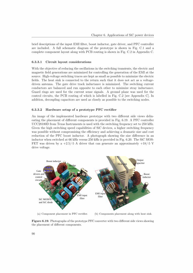
Chapter 6. Applications of SiC power devices
brief descriptions of the input EMI filter, boost inductor, gate driver, and PFC controllerare included. A full schematic diagram of the prototype is shown in Fig. C.1 and acomplete component layout along with PCB routing is shown in Fig. C.2 in Appendix C.
6.3.3.1 Circuit layout considerations
With the objective of reducing the oscillations in the switching transients, the electric andmagnetic field generations are minimized for controlling the generation of the EMI at thesource. High-voltage switching traces are kept as small as possible to minimize the electricfields. The heat sink is connected to the return such that it does not act as a voltage-driven antenna. The gate drive track inductance is minimized. The switching currentconductors are balanced and run opposite to each other to minimize stray inductance.Guard rings are used for the current sense signals. A ground plane was used for thecontrol circuits, the PCB routing of which is labelled in Fig. C.2 [see Appendix C]. Inaddition, decoupling capacitors are used as closely as possible to the switching nodes.
6.3.3.2 Hardware setup of a prototype PFC rectifier
An image of the implemented hardware prototype with two different side views delin-eating the placement of different components is provided in Fig. 6.19. A PFC controllerUCC28180D from Texas Instruments is used with the switching frequency set to 250 kHz.Given the high switching speed capabilities of SiC devices, a higher switching frequencywas possible without compromising the efficiency and achieving a dramatic size and costreduction of the PFC boost inductor. A photograph showing the size difference in aninductor when switched at 66 kHz versus 250 kHz is provided in Fig. 6.20. The SiC MOS-FET was driven by a +2.5/-5 A driver that can generate an approximately +18/-5 Vdrive voltage.
Output
capacitor
SiC MOSFET
and SiC diode
Gate
drivers and
control
circuits
EMI input
filter
Boost inductor
Bridge
rectifier
(a) Component placement in PFC rectifier.
Output
capacitor
EMI input
filter
Boost
inductor
Heat sink
(b) Components placement along with heat sink.
Figure 6.19: Photographs of the prototype PFC converter with two different side views showingthe placement of different components.
90

Chapter 6. Applications of SiC power devices
(a) 66 kHz. (b) 250 kHz.
Figure 6.20: Switching at 66 kHz requires 2 × stacked sendust core, CS358060, with 70-turnsgiving 565 µH, while at 250 kHz, only 1 × stacked sendust core, CS330060, is sufficient leadingto dramatic reduction in size of inductor.
L3-A
attenuates
DM EMI
L1-A – L2-A
attenuates
CM EMI
Bridge rectifier
Two
stage
EMI
filter
CX1
CX2
CX3
CY1
CY2
CY3 CY4
4 × 4n7 F
Figure 6.21: Schematic diagram showing the two-stage EMI filter, the first stage consisting ofinductors, L1−A and L2−A, attenuating the CM EMI, and the second stage with L3−A attenuat-ing DM EMI. Capacitances CY 1–CY 4 (nF range) primarily serve as a CM filter; and CX1–CX3
(µF range), as a DM filter.
A two-stage EMI filter, as shown in Fig. 6.21, was designed and implemented. The firststage consisting of the inductance, L1−A, L2−A, and the capacitances, CY 1–CY 4, attenuatesa common-mode (CM) EMI. The second stage incorporating the inductance, L3−A, andcapacitances, CX1–CX3, attenuates a differential-mode (DM) EMI. The procedure followedin the design of the CM and DM filter is enumerated below.
1. Because the switching transients are the sources of the EMI, the measured DPT wave-forms (time domain) are taken as an input to plot the corresponding frequency domainequivalent to a Fourier transform in MATLAB. This measured original noise is com-pared with the CISPR limits. Selecting the filter topology, as shown in Fig. 6.21, thecorner frequency is calculated such that the attenuation satisfies the limit with an extra6 dB safety margin.
2. First, the CM capacitances, CY 1–CY 4, are limited based on regulations indicating thatthe current-to-ground must not exceed 3 mA at 50/60 Hz. Accordingly, CM induc-tances are calculated using the resonance principle at the computed corner frequency.
91
Chapter 6. Applications of SiC power devices
Then, the CM filter is tested in the MATLAB Simulink model of the PFC converterto check the defined 3 mA leakage current limit.
3. Because the leakage inductance of the CM choke, as well as the boost inductance ofthe PFC stage, help minimize the DM noise, a fairly low DM inductance is selected,namely, 1–4% of the CM inductance. Again, using the resonance equation, the CMcapacitance is computed.
4. The designed filter was simulated in LTSpice employing realistic spice models of thecircuit components, including SiC MOSFET, SiC diode, and EMI filters to check theEMC compliance before building the EMI filter in a laboratory.
Table 6.14 shows the designed EMI filter components for the prototype.
Table 6.14: EMI filter specifications.
CY 1–CY 4, CM capacitances, Ceramic, Class X1/Y2
4 × 4n7F, P10 mm
L1−A, L2−A, CM chokes, EPCOS-TDK, R25 Ring core
T38 material, 19 turns per coil, wire diameter 1.219 mm
2 × 3.6 mH ± 25% @ 1 kHz
L3−A, DM chokes, Micrometal, T106-26 core, 36 turns
wire diameter 1.422 mm, 1 × 120 µH ± 10% @ 1 kHz
CX1–CX3, DM capacitances, MKR, EPCOS, × 2 Class
3 × 1µF, 305 V, P22.5 mm
6.3.4 Experimental results
In this section, the efficiency and EMI evaluation of the prototype PFC converter arepresented. The higher the ripple current in the boost inductance, the higher the AC lossesin it. As a consequence, higher is the EMI because of the potential higher radiations ofmagnetic field. In this work, the SiC devices are switched with 0 Ω gate resistance togetherwith the low parasitic design approach (the highest possible dv/dt and di/dt) with theaim of maximizing the efficiency and measuring the worst case EMI. However, slowingthe SiC MOSFETs would potentially minimize EMI noises with the penalty of higherswitching losses. Fig. 6.22 (a) shows the measured ac mains voltage and current. Clearly,is shapes vs as expected. Fig. 6.22 (b) shows the MOSFET drain-source voltage andinductor current when switched at approximately 250 kHz. The discontinuity at zero-crossing of is is clearly seen because the dead-time comprises a major part with fsw of 250kHz compared with fsw of 66 kHz. Fig. 6.23 (a) and (b) show the drain- and gate-sourcevoltages during the turn-off and turn-on transients, respectively, illustrating the cleanswitching of an SiC MOSFET.
92

Chapter 6. Applications of SiC power devices
s
v
si
(a) Measured vs, and is.
L
i
ds
v
(b) Measured vds, and iL, at ≈ 250 kHz.
Figure 6.22: Oscilloscope graphs at a switching frequency of roughly 250 kHz. (a) Illustrationof ac mains current, is, shaping ac mains voltage, vs. (b) With fsw of 250 kHz, boost inductorcurrent, ∆iL, is 0.7 A, while it was 1.5 A with fsw of 66 kHz. Influence of dead-time is seen asthe discontinuity at zero-crossing of is.
dsv
gsv
(a) vds and vgs during turn-off.
dsv
gsv
(b) vds and vgs during turn-on.
Figure 6.23: Measured drain-source voltage, vds, and gate-source voltage, vgs, illustrating theclean switching of an SiC MOSFET. The gate oscillations are within the region where the deviceis beginning to partly turn on and transiting through the Miller plateau. This initial ringing isdue to the input gate capacitance and the circuit parasitic inductance. Thereafter, the changein drain current is minor, resulting in insignificant ringing in vds during a turn on.
6.3.4.1 Efficiency evaluation
The simulated efficiency of the rectifier as a function of the output power for vs = 230 Vis shown in Fig. 6.24, together with the measurement results taken using a YokogawaWT3000 power analyzer. As can be seen, the simulated results of the converter followa similar pattern as the measured efficiency over a wide range of output power, and thediscrepancy between the two is primarily due to two reasons. First, the simulated casedoes not consider the core losses in the boost inductor or the input EMI filter losses,whereas the measured case includes the overall losses in the PFC rectifier. Second, tomeasure such a high efficiency, an error introduced when using a power analyzer is alsocritical. Nonetheless, the converter achieves an efficiency of above 97% for > 60% ofthe rated load with a peak efficiency of 97.2%, and is well above the 80 PLUS efficiencyrequired over the entire load range.
93

Chapter 6. Applications of SiC power devices
0 200 400 600 800 1000
8889909192939495969798
Figure 6.24: Illustration of the simulated and measured efficiency of the PFC rectifier as afunction of the output power, indicating that the converter achieves an efficiency of above 97%for a rated load of >60% with a peak efficiency of 97.2%. The measurements were taken usinga prototype converter with a Yokogawa WT3000 power analyzer.
6.3.4.2 EMI evaluation
A standard line impedance stabilizing network (LISN) and an EMC analyzer (AgilentE7401A) were used for measuring the EMI. Fig. 6.25 shows the measured conducted EMIemission (within the frequency range of 150 kHz–30 MHz) of the prototype PFC rectifierat an input voltage of 230 V and an output power of 1 kW at two different switchingfrequencies, 66 and 250 kHz. Compared to 66 kHz switching, at 250 kHz, the EMI noiseshifts toward the right slightly, and then increases by approximately 10 dB (23-13 =10 dB) over the entire spectra applied, given the same EMI filter size. Alternatively, itcan be stated that, as the switching frequency increases, the filter size increases if thesame noise level needs to be maintained. For the chosen MOSFET, the DPT-measuredparasitic oscillations were within the range of 25 MHz. Interestingly, the EMI noises inthe corresponding frequency range are augmented, which is clearly shown in Fig. 6.25.This was also corroborated through a simulation conducted in LTSpice by varying theswitching loop inductance and observing the noise within the frequency domain plot.
100
80
60
40
20
0
-20 150 k 1 M 10 M 30 M
Frequency [Hz]
Nois
e [d
B
V]
Avg Limit
QP Limit CISPR 11 Class B @ 66 kHz
≈ 23 dB
Parasitic oscillation
amplifies noise
(a) Conducted EMI at a switching frequency of 66 kHz.
94

Chapter 6. Applications of SiC power devices
100
80
60
40
20
0
-20 150 k 1 M 10 M 30 M
Frequency [Hz]
Nois
e [d
B
V]
CISPR 11 Class B
Avg Limit QP Limit @ 250 kHz
shift
≈ 13 dB
Parasitic oscillation
amplifies noise
(b) Conducted EMI at a switching frequency of 250 kHz.
Figure 6.25: Conducted maximum peak and average EMI noise emissions of the prototype PFCrectifier at an input voltage of 230 V and an output power of 1 kW at two different switchingfrequencies, namely, 66 and 250 kHz. All measurements are below the quasi peak (QP) andaverage (Avg) limits, and thus meet the CISPR 11 regulation for Class B equipment. Comparedto 66 kHz, a 250 kHz switching incurs a higher noise provided an identical EMI filter.
6.3.5 Summary and conclusion
The main conclusions from this work are summarized below.
1. Employing low-loss SiC power devices in the boost stage, the efficiency was evaluatedin a classic boost PFC topology, the results of which revealed that the major converterloss is comprised of a diode rectifier part, which is particularly pronounced at a low-lineas compared to a high-line voltage.
2. A comparison between the efficiencies evaluated using a simple look-up table inputfrom a double-pulse test follows the pattern measured using a power analyzer meetingthe 80 PLUS efficiency regulation over the entire load range with an excellent margin.
3. The conducted EMI in the prototype converter was found to comply with the CISPR11 standard. It was also concluded that, owing to the increase in switching frequencyfrom 66 to 250 kHz, the emissions are increased by roughly 10 dB throughout theentire frequency range (150 kHz to 30 MHz). Moreover, it was revealed that EMInoise is augmented at the corresponding ringing frequency given by the parasitic inthe commutation loop.
4. Increasing the switching frequency drastically minimizes the boost inductor size; how-ever, the increase in the input EMI filter size might offset the high-power density target,and thus an optimal switching frequency should be chosen.
5. Clean switching of the state-of-the-art SiC devices was illustrated to substantiate thedesign of a low-parasitic layout.
95

Chapter 6. Applications of SiC power devices
96

Chapter 7
Low-inductive converter designconsiderations
The information presented in this chapter is based on publications C4 and C5, the mainpurpose of which is to address the following research challenge.
SiC transistors have the potential to switch extremely fast. Often turn-off di/dt is re-duced to limit the turn-off over voltages due to the stray inductances in the commutationloops. Thus, the potential low switching losses are not met. One of the benefits of designswith SiC devices is the possibility of low switching losses and therefore high switching fre-quencies. This opens up for a paradigm shift in power electronics. For utilizing the fastswitching potential, a low-inductive circuit layout of the commutation loop consisting ofthe transistor, diode, connections and the DC-link capacitor is indispensable. Extensiveresearch on low-inductive transistor case and busbars has, to date, been conducted by sev-eral research groups [25–28]. Employing low stray inductance DC-link capacitors is a mustfor realizing the low stray inductance designs. The method used to connect the DC-linkcapacitors to the system, such as the busbar, is equally important. The work analyzes thegeometry and orientation of the DC-clamping capacitor for minimizing the SiC transistorturn-off over voltages. In addition, by reviewing the commercially available low inductanceDC-link capacitors with different physical sizes and terminations, this thesis presents thedesign of a DC-link for a 100 kW full-bridge AC-DC-AC converter. Two approaches; first,measuring the parasitics of the components themselves, such as capacitor and transistormodule by impedance analyzer; and, second, computing the parasitics of the bussing struc-ture and connections via finite element analysis tool; are adopted throughout this work.Based on this, the breakdown of the total switching loop stray inductance contributed byeach parts is illustrated. A few design examples for further minimizing the switching loopstray inductance when used SiC modules and discrete SiC packages are also provided.
7.1 Introduction
In a diode-clamped inductive load buck converter, as shown in Fig. 7.1 (a), the transistorcurrent basically stays constant until its voltage has reached the supply voltage. Thenthe current will commutate via the freewheeling diode (D1) to a DC protection capacitor(CDC). The parasitic inductances of the commutation loop are: internal in the compo-nents themselves; for instance, in the semiconductor devices (denoted by red coils), and inthe CDC (Lbyp−ESL); and in the busbar (Lbusbar) [1]. Additionally, the method to connect
97

Chapter 7. Low-inductive converter design considerations
these components to the busbar also shares a considerable portion of stray inductances,which are indicated by Ltrans−module−con and Lbyp−con. During the turn-on process, theseparasitic inductances are charged, and, during the turn-off process, they are discharged.The transistor turn-off over voltage can be expressed as: Lloop · di/dt, where di/dt isdictated by the transistor properties and its gate drive. A typical turn-off transient withtwo different loop inductances (Lloop) is shown in Fig. 7.1 (b), which illustrates that thehigher the Lloop, the higher the over voltage, the lower the current slew rate [17]. It isnoteworthy that voltage overshoot is increased although di/dt is reduced, the reason beinga significantly higher increase in Lloop than the decrease in di/dt. Furthermore, for thesame Lloop, this over voltage is more noticeably amplified for the SiC transistor comparedto the Si transistor because the former switches extremely fast. For example, di/dt perchip area is measured to be 5.1 A/ns/cm2 in SiC MOSFET and 2.2 A/ns/cm2 in Si IGBT,i.e., di/dt is higher by a factor of 2.3 in SiC MOSFET compared to Si IGBT [18]. Often,SiC is slowed down to the level of Si to operate it safely with a penalty of higher switchinglosses. Thus, it is crucial to design a low-inductive layout to fully utilize the fast switchingpotential of SiC transistor.
600 V
busbarL
byp conL
byp ESLL
dsI
dsV
Induct
or
Transistor
module
supply conL
Double Pulse
1D
trans moduleL
DCC
trans module-conL
(a) A diode-clamped inductive load circuit.
0 100 200 300 400 500 600time [ns]
-20
0
20
40
60
80
100
120
(b) Turn-off transient.
Figure 7.1: (a) Buck converter with various possible stray inductances in the loop, (b) turn-offtransient illustrating the importance of having lower Lloop.
In low power electronics area, there exist several application notes and publicationsconcerning low inductance capacitors [214,215]. However, there is limited literature avail-able concerning those in the high power electronics area. In [216], internal inductance ofDC-link power capacitors are addressed, but the method to connect them is not covered.First, this work presents some of the dielectric materials available in market in Section 7.2.Then the impact of physical dimensions of structure on the stray inductances and capac-itances is discussed in Section 7.3. Thereafter, Section 7.4 reviews the current availablelow inductance DC-link capacitors with different physical dimensions and terminations,and measures the Lbyp−ESL associated with them using impedance analyzer, E4990. For afair comparison, the normalization is performed with two different parameters; first, withrespect to the highest capacitance value, and second, with respect to the largest ripplecurrent possessed by the selected capacitors. Following this, the 3D finite element method(FEM) models are built for axial and circular terminated capacitors in Section 7.5. An-sys Q3D tool is used for extracting the parasitics of the required bussing structures and
98

Chapter 7. Low-inductive converter design considerations
plotting the current density distribution. Additionally, by highlighting the two differentorienting methods for capacitors, this work provides guidelines for designing and orientingthem such that Lbyp−ESL and Lbyp−con, as labelled in Fig. 7.1 (a), are minimum, wherethe main contribution of this work lies.
Moreover, a 100 kW AC-DC-AC converter is simulated in MATLAB for finding thecurrent stress in the DC-link capacitor in Section 7.6. Dimensioning of the DC-link capac-itance for satisfying the defined voltage ripple is also included in this section. Employingeach of the low-inductive types of capacitor under study, five DC-link busbars are builtand simulated in Q3D. Subsequently, the parasitic inductances encompassed by variousparts, such as Ltrans−module−con, Lbyp−con, and power supply connection (Lsupply−con) areaccessed. For providing a comprehensive overview of the proportion of stray inductancesincorporated by different parts, inductances internal to the components themselves, forexample, capacitor and transistor module are measured by impedance analyzer. An ex-ample of a complete busbar employing an optimal capacitor solution, in terms of cost andloop inductance factors, is also demonstrated. Looking into the current density distribu-tion plot in the busbar, two different phenomenons can be distinguished: (a) the partsthat are bypassed, and (b) the most stressed parts construing the major current flow.In the quest of further minimizing stray inductance, Section 7.7 and Section 7.8 exem-plify low-inductive busbar designs using SiC modules and discrete SiC devices. Finally,Section 7.9 presents the most important conclusions.
7.2 Theoretical background for the selection of di-
electric material
Different dielectric materials are available in market. Some of them are listed in Table 7.1.The thinner the dielectric, the stronger the magnetic coupling between thepositive and the negative plates. Kapton and Mylar are the thinnest ones in thelist. Considering the breakdown strength, dielectric constant, operating temperature andthickness, either Mylar or Kapton are preferred as dielectric material. Fig. 7.2provides the photograph of the dielectric materials; Mylar and Kapton.
Table 7.1: List of insulating materials with breakdown voltage, dielectric constant and contin-uous temperature.
Insulating Material Breakdown Dielectric Constant ContinuousTypes voltage (kV/mil ∗) (Unitless) temperature (C)
Kapton 5 3.7 400Mylar (PET) 7.5 3.3 105Teonex (PEN) 5 3.4 140
Epoxy glass (FR4) 1.25 4.3 140Nomex 0.43-0.84 1.6 220
Tedlar (PVF) 3.5 11 105Epoxy powder coating 0.8 4 130
∗ 1 mil = 0.0254 mm.
99

Chapter 7. Low-inductive converter design considerations
(a) Mylar. (b) Kapton.
Figure 7.2: Photograph showing the dielectric material; Mylar and Kapton.
7.3 Impact of geometry on stray inductance and ca-
pacitance
In this section, the stray inductance (Lstray) and distributed capacitance (Cdis) of coplanar,planar and coaxial structures are studied through basic physics-based expressions, as givenby (7.1)–(7.5) [217–219]. The dimensions used are: width (w), length (l), distance betweenthe positive and the negative plates (h), diameter of the inner conductor (d), and diameterof the outer conductor (D). The remaining variables used in the equations are: εr; relativepermittivity of the dielectric, and ε0; permittivity of the free space. Likewise, µr is therelative permeability of the medium and µ0 is permeability of the free space. For greaterclarity, the dimensions used in these equations are labelled in Fig. 7.3.
Lstray, coplanar =µ0 · µr
π· cosh−1 w + t
w· l, t w, (7.1)
Lstray, planar = µ0 · µr ·h · lw, w h (7.2)
Lstray, coaxial =µ0 · µr
2π· ln D
d· l (7.3)
Cdis, planar = ε0 · εr ·w · lh
(7.4)
Cdis, coaxial =2π · ε0 · εrln D
d
· l (7.5)
(a) Coplanar.
h
(b) Planar.
d/2 D/2
l
h
(c) Coaxial.
Figure 7.3: Example of coplanar (a), planar (b) and coaxial structures with dimensions. Thecoaxial structure cancels the magnetic field more effectively than the coplanar and planar ones.
Fig. 7.4 (a) shows the plot of (Lstray) versus w/l (or d/l) ratio for planar and coaxialstructures. Apparently, there is the highest reduction in Lstray for w/l (or d/l) ratio up to
100

Chapter 7. Low-inductive converter design considerations
1, which suggests that this ratio should be ≥1. In addition, the closer the opposite plates,the lower the inductance. Nonetheless, for the same separation between the oppositeplates, the coaxial structure gives four times lower Lstray than the planar structure. Incontrast, for the same conditions, the coaxial structure entails three times higher Cdis
than the planar structure, as conveyed in Fig. 7.4 (b). Of special note is that Cdis acts asa filter for instance, for reducing EMI, and it is preferred to be in the higher range, andthus the dielectric with minimum thickness and high relative permittivity is desirable. Inconclusion, the coaxial structure cancels the magnetic field more effectively thanthe planar and coplanar approaches, however, it not easy to realize a completeplanar or coaxial design in all the places like terminations and clearances.
0 0.5 1 1.5 2 2.5 30
10
20
30
40
Lst
ray,
pla
nar [n
H]
0
2
4
6
8
10
Lst
ray,
coa
xial
[nH
]
h = 1 mm - planarh = 2.5 mm - planarh = 1 mm - coaxialh = 2.5 mm - coaxial
(a) Lstray plot with varying w/l or d/l ratio.
0 2 4 6 8 10 120
50
100
150
Cdi
s, p
lana
r [nF
/m]
0
150
300
450
Cdi
s, c
oaxi
al [n
F/m
]
h = 1 mm - planarh = 2.5 mm - planarh = 1 mm - coaxialh = 2.5 mm - coaxial
(b) Cdis plot with varying dielectric constant.
Figure 7.4: Lstray plot of planar versus coaxial structures illustrates the highest reduction inLstray for w/l (or d/l) ratio upto 1. Clearly, the smaller the h, the lower the Lstray. For the sameh, Lstray is lower by a factor of 4 for the coaxial structure compared to the planar structure.µr is taken as 1 while plotting Lstray. Cdis plot of planar versus coaxial structures conveys thatfor the same h, Cdis is higher by a factor of 3 for the coaxial structure compared to the planarstructure. As Cdis is a filter, it is preferred to be in the higher range, and thus the dielectricwith minimum thickness and high relative permittivity is desirable.
7.4 Selection of low inductance DC-link capacitors
In this section, a brief description of the selected low inductance DC-link capacitors ispresented. Fig. 7.5 provides a photograph of these capacitors, namely, DCL capacitor,MKR capacitor, Ring capacitor, Coaxial capacitor and Ceralink capacitor. The first fourare film type and the last one is a Ceramic type with different dielectric material than in aclassic ceramic capacitor. In reference [216], it is mentioned that the capacitance increaseswith increasing voltage in the dielectric used for Ceralink type, while the opposite is truein the class 2 ceramic materials used for multilayer ceramic capacitors. Primarily, themechanical interface of capacitors are decided by their voltage and current ratings. Fora fair comparison, capacitors with equal voltage ratings (900 V) have been chosen. Theelectrical specification of the selected capacitors is shown in Table 7.2. The capacitanceand ripple current rating (Iripple) are from data sheet, where the latter is taken for 85 C[220–223]. The effective series inductance (Lbyp−ESL) is measured using an impedanceanalyzer, E4990.
101

Chapter 7. Low-inductive converter design considerations
(a) DCL. (b) MKR. (c) Ring. (d) Coaxial. (e) Ceralink.
Figure 7.5: Photograph of five different commercially available low inductance capacitors,where (a) is a DCL capacitor (45 mm separation between the opposite screws), (b) is an MKRcapacitor (24 mm separation between the opposite pins), (c) is a Ring capacitor, (d) is a Coaxialcapacitor, and (e) is a Ceralink capacitor (7.62 mm separation between the opposite pins).
Table 7.2: Electrical specification of low inductance DC-link capacitors.
Capacitor type Capacitance Iripple Lbyp−ESL Cost& parameters (µF) (A) @85C (nH) (e)
DCL 150 50 14.85 18MKR 95 45 4.85 25Ring 215 175 10.2 170
Coaxial 20 20 6.7 10Ceralink 5 25 3.5 52
Table 7.3: Parameters normalized to capacitance of Ring capacitor.
Capacitor type No. of Iripple Lbyp−ESL Total cost& parameters capacitors (A) (nH) (e)
DCL 2 100 7.42 36MKR 3 135 1.61 75Ring 1 175 10.2 170
Coaxial 11 220 0.61 110Ceralink 43 1075 0.08 2236
Table 7.4: Parameters normalized to ripple current of Ring capacitor.
Capacitor type No. of Capacitance Lbyp−ESL Total cost& parameters capacitors (µF) (nH) (e)
DCL 4 600 3.71 72MKR 4 380 1.21 100Ring 1 215 10.20 170
Coaxial 9 180 0.74 90Ceralink 7 35 0.50 364
Considering Lbyp−ESL of a single capacitor, Ceralink has the lowest value followed byMKR, Coaxial, Ring, and DCL. Prominently, Ceralink has the largest ripple current per
102
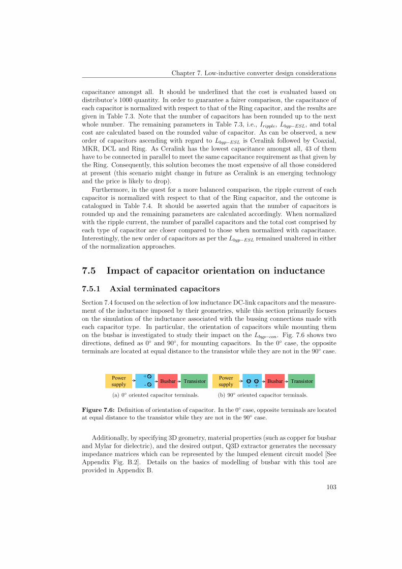
Chapter 7. Low-inductive converter design considerations
capacitance amongst all. It should be underlined that the cost is evaluated based ondistributor’s 1000 quantity. In order to guarantee a fairer comparison, the capacitance ofeach capacitor is normalized with respect to that of the Ring capacitor, and the results aregiven in Table 7.3. Note that the number of capacitors has been rounded up to the nextwhole number. The remaining parameters in Table 7.3, i.e., Iripple, Lbyp−ESL, and totalcost are calculated based on the rounded value of capacitor. As can be observed, a neworder of capacitors ascending with regard to Lbyp−ESL is Ceralink followed by Coaxial,MKR, DCL and Ring. As Ceralink has the lowest capacitance amongst all, 43 of themhave to be connected in parallel to meet the same capacitance requirement as that given bythe Ring. Consequently, this solution becomes the most expensive of all those consideredat present (this scenario might change in future as Ceralink is an emerging technologyand the price is likely to drop).
Furthermore, in the quest for a more balanced comparison, the ripple current of eachcapacitor is normalized with respect to that of the Ring capacitor, and the outcome iscatalogued in Table 7.4. It should be asserted again that the number of capacitors isrounded up and the remaining parameters are calculated accordingly. When normalizedwith the ripple current, the number of parallel capacitors and the total cost comprised byeach type of capacitor are closer compared to those when normalized with capacitance.Interestingly, the new order of capacitors as per the Lbyp−ESL remained unaltered in eitherof the normalization approaches.
7.5 Impact of capacitor orientation on inductance
7.5.1 Axial terminated capacitors
Section 7.4 focused on the selection of low inductance DC-link capacitors and the measure-ment of the inductance imposed by their geometries, while this section primarily focuseson the simulation of the inductance associated with the bussing connections made witheach capacitor type. In particular, the orientation of capacitors while mounting themon the busbar is investigated to study their impact on the Lbyp−con. Fig. 7.6 shows twodirections, defined as 0 and 90, for mounting capacitors. In the 0 case, the oppositeterminals are located at equal distance to the transistor while they are not in the 90 case.
Busbar Transistor+
-
Power
supply
(a) 0 oriented capacitor terminals.
Busbar Transistor+-
Power
supply
(b) 90 oriented capacitor terminals.
Figure 7.6: Definition of orientation of capacitor. In the 0 case, opposite terminals are locatedat equal distance to the transistor while they are not in the 90 case.
Additionally, by specifying 3D geometry, material properties (such as copper for busbarand Mylar for dielectric), and the desired output, Q3D extractor generates the necessaryimpedance matrices which can be represented by the lumped element circuit model [SeeAppendix Fig. B.2]. Details on the basics of modelling of busbar with this tool areprovided in Appendix B.
103

Chapter 7. Low-inductive converter design considerations
7.5.1.1 DCL capacitor
Fig. 7.7 depicts the simulated busbar for DCL capacitor with 45 mm separation betweenthe opposite screws, where (a) is with 0 orientation and (b) is with 90 orientation alongwith the corresponding Lbyp−con labelled in the respective current density plots. Thecurrent flows from the capacitor (source) to the load (sink) and is indicated by an arrowhead. Self-inductances (L11 and L22) of the opposite plates are almost equal in the formercase, while there is a large difference between those in the latter case, and the results aresummarized in Table 7.5. It is worth emphasizing that the 0 case showed around 20%lower Lbyp−con compared to the 90 case. This is a result of there being a strongerflux linkage between the opposite plates in the former orientation comparedto the latter.
(a) 45 mm seperation with 0.
Source
Sink
11.15 nH
(b) 45 mm seperation with 90.
Figure 7.7: Simulated busbar for DCL capacitor with 45 mm separation between the oppositescrews. Orientation in (a) has lower loop inductance than in (b).
(a) 24 mm seperation with 0.
Sink
Source
5.43 nH
(b) 24 mm seperation with 90.
Figure 7.8: Simulated busbar for DCL capacitor with 24 mm separation between the oppositescrews. Orientation in (a) has lower loop inductance than in (b).
DCL capacitors are also available with 24 mm separation distance and the currentdensity plot is shown in Fig. 7.8 (a) with 0 orientation and (b) with 90 orientation.Simulation showed that the smaller the distance between the opposite screwholes, the lower the Lbyp−con. Capacitors with 24 mm separation showed around 47%
104
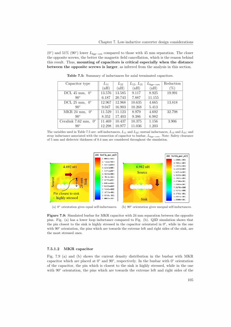
Chapter 7. Low-inductive converter design considerations
(0) and 51% (90) lower Lbyp−con compared to those with 45 mm separation. The closerthe opposite screws, the better the magnetic field cancellation, which is the reason behindthis result. Thus, mounting of capacitors is critical especially when the distancebetween the opposite screws is larger, as inferred from the analysis in this section.
Table 7.5: Summary of inductances for axial terminated capacitors.
Capacitor type L11 L22 L12, L21 Lbyp−con Reduction(nH) (nH) (nH) (nH) (%)
DCL 45 mm, 0 13.576 13.585 9.117 8.925 19.99190 6.187 20.743 7.887 11.155
DCL 25 mm, 0 12.967 12.968 10.635 4.665 13.81890 9.047 16.903 10.268 5.413
MKR 24 mm, 0 11.529 11.123 8.979 4.692 32.79890 8.352 17.403 9.386 6.982
Ceralink 7.62 mm, 0 11.469 10.437 10.375 1.156 3.90690 12.298 10.977 11.036 1.203
The variables used in Table 7.5 are: self-inductances, L11 and L22; mutual inductances, L12 and L21; andstray inductance associated with the connection of capacitor to busbar, Lbyp−con. Note: Safety clearanceof 5 mm and dielectric thickness of 0.4 mm are considered throughout the simulation.
(a) 0 orientation gives equal self-inductances.
Source
Sink
6.982 nH
(b) 90 orientation gives unequal self-inductances.
Figure 7.9: Simulated busbar for MKR capacitor with 24 mm separation between the oppositepins. Fig. (a) has a lower loop inductance compared to Fig. (b). Q3D simulation shows thatthe pin closest to the sink is highly stressed in the capacitor orientated in 0, while in the onewith 90 orientation, the pins which are towards the extreme left and right sides of the sink, arethe most stressed ones.
7.5.1.2 MKR capacitor
Fig. 7.9 (a) and (b) shows the current density distribution in the busbar with MKRcapacitor which are placed at 0 and 90, respectively. In the busbar with 0 orientationof the capacitor, the pin which is closest to the sink is highly stressed, while in the onewith 90 orientation, the pins which are towards the extreme left and right sides of the
105
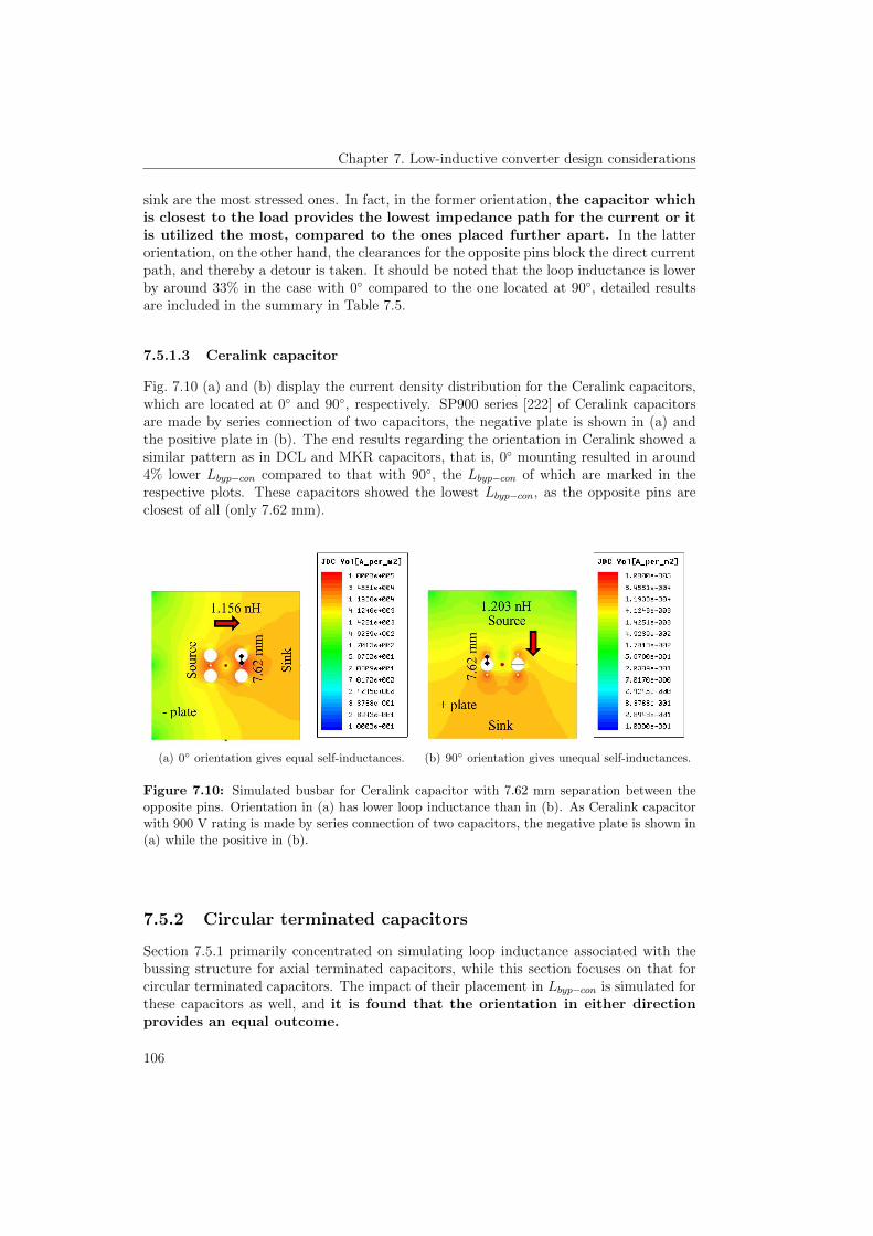
Chapter 7. Low-inductive converter design considerations
sink are the most stressed ones. In fact, in the former orientation, the capacitor whichis closest to the load provides the lowest impedance path for the current or itis utilized the most, compared to the ones placed further apart. In the latterorientation, on the other hand, the clearances for the opposite pins block the direct currentpath, and thereby a detour is taken. It should be noted that the loop inductance is lowerby around 33% in the case with 0 compared to the one located at 90, detailed resultsare included in the summary in Table 7.5.
7.5.1.3 Ceralink capacitor
Fig. 7.10 (a) and (b) display the current density distribution for the Ceralink capacitors,which are located at 0 and 90, respectively. SP900 series [222] of Ceralink capacitorsare made by series connection of two capacitors, the negative plate is shown in (a) andthe positive plate in (b). The end results regarding the orientation in Ceralink showed asimilar pattern as in DCL and MKR capacitors, that is, 0 mounting resulted in around4% lower Lbyp−con compared to that with 90, the Lbyp−con of which are marked in therespective plots. These capacitors showed the lowest Lbyp−con, as the opposite pins areclosest of all (only 7.62 mm).
(a) 0 orientation gives equal self-inductances.
Source
Sink
1.203 nH
(b) 90 orientation gives unequal self-inductances.
Figure 7.10: Simulated busbar for Ceralink capacitor with 7.62 mm separation between theopposite pins. Orientation in (a) has lower loop inductance than in (b). As Ceralink capacitorwith 900 V rating is made by series connection of two capacitors, the negative plate is shown in(a) while the positive in (b).
7.5.2 Circular terminated capacitors
Section 7.5.1 primarily concentrated on simulating loop inductance associated with thebussing structure for axial terminated capacitors, while this section focuses on that forcircular terminated capacitors. The impact of their placement in Lbyp−con is simulated forthese capacitors as well, and it is found that the orientation in either directionprovides an equal outcome.
106

Chapter 7. Low-inductive converter design considerations
7.5.2.1 Ring capacitor
In the chosen Ring capacitor [223], eight terminal pairs are evenly spaced around thecircumference. It is large in terms of both volume and weight. The ratio of diameter(225 mm) to height (50 mm) is 4.5 (1), resulting in low Lbyp−con for the given capaci-tance and ripple current rating. Fig. 7.11 illustrates the current density distribution andthe associated Lbyp−con for it. Because of the larger separation distance between the op-posite screws and larger clearances needed for screw holes, the ring type has a larger loopinductance, as shown in Table. 7.6.
Figure 7.11: Simulated busbar for Ring capacitor (SBE) resulted in equal Lbyp−con in bothorientations. This capacitor is large in terms of both size and weight. The bussing structure andthe clearance holes are also larger compared to the rest of the capacitors under consideration.
7.5.2.2 Coaxial capacitor
In the Coaxial capacitor [221], three pin pairs are evenly spaced around the circumference.It is a PCB mounted type and has a relatively smaller physical size, termination pins andcapacitance compared to the Ring capacitor. The manufacturer has chosen the diameterand height to be almost equal in order to realize low Lbyp−ESL. The simulated busbaris illustrated in Fig. 7.12, and the details about inductance matrices are provided inTable. 7.6.
Table 7.6: Summary of inductances for circular terminated capacitors.
Capacitor type L11 L22 L12, L21 Lbyp−con
(nH) (nH) (nH) (nH)Ring 24.770 12.202 15.933 5.430
Coaxial 9.994 9.094 8.668 1.752
The variables used in Table 7.6 are: self-inductances, L11 and L22; mutual inductances, L12 and L21; andstray inductance associated with connection of capacitor to busbar, Lbyp−con. Note: Safety clearance of5 mm and dielectric thickness of 0.4 mm are considered throughout the simulation.
107

Chapter 7. Low-inductive converter design considerations
1.75 nH
Figure 7.12: Simulated busbar for Coaxial capacitor (FTCAP). Orientation in either directionprovides an equal outcome. Lbyp−con is smaller compared to that of the Ring capacitor becausethe opposite pin pairs are closer and smaller.
7.6 Design of DC-link for AC-DC-AC converter
In this section, there are three main objectives. The first objective concerns sizing ofthe DC-link capacitor in an AC-DC-AC converter, which is covered in Section 7.6.1.The second objective relates to comparing the stray inductance constituted by variouscomponents and their connections, which is presented in Section 7.6.2. The third goalentails exemplifying a DC-link busbar design employing Coaxial capacitor, and is includedin Section 7.6.3.
7.6.1 Sizing the DC-link capacitor
A series-resonant converter topology for an induction heating application is shown inFig. 7.13. The DC-link capacitor (CDC) is stressed from two sides: rectifier and inverter.First, in order to find the ripple current share from the 6-pulse bridge rectifier side, asimulation is performed in MATLAB for a 100 kW converter with a DC-link voltage of640 V. At 360 Hz (6 × 60 Hz, 60 Hz being the AC line frequency), the ripple current issimulated to be 7.2 A. Second, to find the ripple current which comprises the inverter part,the full-bridge series-resonant inverter is switched at 300 kHz for an output current (Iout) of180 A, which resulted in the ripple current of 80.5 A in the CDC . Adding the contributionfrom the rectifier part and the inverter part, the aggregate ripple current (Ic) capacity ofcapacitor becomes 87.7 A. Simultaneously, the DC-link capacitor should be sized such thatthe defined ripple voltage requirement (<10%) in a converter is ensured. The simulationwas performed with the capacitance of 180 µF which gave the ripple voltage of 45 V;7% of the DC-link voltage. When using 35 µF of Ceralink capacitors, as obtained fromthe normalization in Section 7.4, the ripple voltage will cross the defined ripple limit, thesolution would be to connect an additional 29 Ceralink capacitors. However, this solutionwould be the most expensive of all. On the other hand, all the remaining capacitors givea ripple voltage well below the defined margin.
7.6.2 Comparison of stray inductance shared by various parts
In this section, FEM simulation is used to extract the stray inductance created by theconnection of power supply, capacitor, and transistor module, however, the ones associated
108

Chapter 7. Low-inductive converter design considerations
cI
Transistor
module 1
Transistor
module 2
DCC
300kHzsw
f
60Hzline
f
640VDC
V
,180A
out rmsI
T4
T3
T2
T1
6-pulse
diode
rectifier
High-frequency
transformer
Metallic piece
Coil
AC
Load 100 kW
Figure 7.13: Schematic diagram of AC-DC-AC converter for an induction heating application.Capacitor (CDC) is stressed partly from the front end 6-pulse diode rectifier but primarily fromthe 300 kHz switched series-resonant inverter. For instance, for the given 100 kW converter, thefront end current stress by 360 Hz component is simulated to be 7.2 A and the current stressfrom the inverter part is 80.5 A, so the total capacitor current (Ic) is 87.7 A. With capacitanceof 180 µF, the ripple voltage resulted in being 7% of DC-link voltage.
internal to the capacitor and the transistor module are measured using an impedanceanalyzer. Five different 3D models of the DC-links are built employing each type ofthe selected capacitors. The number of capacitors is according to the normalization withrespect to the ripple current capacity, as shown in Table 7.4. It should be highlighted thatLbyp−con for the axial terminated capacitors is simulated with 0 orientation, as explainedin Section 7.5.1. Furthermore, for the DCL capacitor, the case with 24 mm separation ischosen.
Table 7.7 depicts the total switching loop stray inductance (Lloop) which is the com-posite of the stray inductance contributed by all the components and connections inthe switching loop. For instance, adding the inductance comprised by the capacitorpart (Lbyp−ESL + Lbyp−con = 0.74 + 0.55 = 1.29 nH) and the transistor module part(Ltrans−module + Ltrans−module−con = 15 + 5.96 = 20.9 nH), Lloop is reckoned to be 22.25 nHfor the busbar with Coaxial capacitor. Note that FEM simulation was performed withand without the supply part, but the simulated results remained unchanged. This is ob-vious because the supply part of the busbar is bypassed. Since Lsupply−con is bypassed, itis not accounted while computing Lloop.
Table 7.7: Summary of switching loop inductance.
Capacitor type Lbyp−ESL Lbyp−con Lloop Improvement& parameters (nH) (nH) (nH) (%)
DCL 3.71 1.61 26.67 31.28MKR 1.21 1.94 24.52 36.82Ring 10.20 5.43 38.81 0
Coaxial 0.74 0.55 22.25 42.66Ceralink 0.50 0.26 21.89 43.59
Note: Lloop = (Lbyp−ESL + Lbyp−con + Ltrans−module + Ltrans−module−con) //Lsupply−con.
109

Chapter 7. Low-inductive converter design considerations
As can be observed from the table, the solution with Ring capacitor resulted in beingthe most inductive followed by DCL, MKR, Coaxial, and Ceralink. In the last columnlabelled as “Improvement” the percentage reduction in the total switching loop strayinductance compared to that when using the Ring capacitor is shown. In addition, theshare of module part and the capacitor part can be visualized by the bar chart in Fig. 7.14.Employing DCL and MKR capacitors, the total loop inductance is improved by around31% and 37%, correspondingly, taking Lloop imposed by Ring capacitor as a reference.Similarly, using the solution with Coaxial and Ceralink capacitors, the loop inductance isimproved the most; by approximately 43% and 44%, respectively, compared to the loopinductance impressed by the Ring capacitor solution.
Likewise, from the bar chart, it is also clear that the majority of switching loopstray inductance is shared by the transistor module part. Apparently, the internalinductance of the transistor module is equivalent to that composed by the Ring capacitorin total. In fact, SiC MOSFETs are packaged in the same standard plastic package asused for Si IGBT modules, which is the reason for such a high inductance in the transistormodule.
DCL MKR Ring Coaxial CeralinkType of capacitors
0
10
20
30
40
50
Stra
y in
duct
ance
[nH
]
-31.28% -36.82% -42.66% -43.59%
Figure 7.14: Breakdown of switching loop stray inductance in a 100 kW AC-DC-AC con-verter. The legends in bar chart are: internal parasitic inductance of the transistor module(Ltrans−module), stray inductance from the transistor module connection (Ltrans−module−con),inductance associated internally in the capacitor (Lbyp−ESL), and stray inductance from thebypass capacitor connection (Lbyp−con). The stray inductance shared by Ltrans−module andLtrans−module−con are the most critical ones and have to be further reduced.
7.6.3 Exemplifying a DC-link busbar design with coaxial capac-itor
An example of the simulated DC-link busbar employing nine coaxial capacitors in parallelis provided in Fig. 7.15. This combination possesses the total ripple current capacity of175 A. With a capacitance of 180 µF, the ripple voltage in the DC-link is 45 V as perthe MATLAB simulation, which is 7% of the total DC-link voltage (640 V). It is worthmentioning that for maintaining the ripple voltage within 10%, the capacitance was chosento be 180 µF, which, in turn, ended up with double the ripple current capacity than that
110

Chapter 7. Low-inductive converter design considerations
Figure 7.15: Simulated DC-link busbar with nine coaxial capacitors resulting in the totalbussing stray inductance of 6.5 nH. Note that this DC-link has a total capacitance of 180 µFand ripple current capacity of 175 A. Clearly noticeable is the higher current density towards thetransistor module connection side (right side), compared to the supply side (left side) indicatingthat the capacitors away from the transistor module are bypassed, that is, capacitor closer tothe switching device provides a low inductance path for switching transients.
of the simulated value. Furthermore, it is noticeable from Fig. 7.15 that current densityis higher towards the transistor module side (right side), indicated by the redcolor, compared to the supply side, indicated by the blue color. Observing thispattern in the current density plot, it can be inferred that the components away from thetransistor module are bypassed. To rephrase it, the capacitor closer to the switchingdevice provides a low inductance path for switching transients.
7.7 Example of a low-inductive busbar design for SiC
MOSFET modules
The major parts of the earlier sections dealt with minimizing the stray inductance com-prised by the DC-link capacitors. However, this section primarily focusses on reducingthose contributed by the module connection, Ltrans−module−con apart from Lbyp−con. Ex-amples of busbars for single versus multiple screw holes modules with single and doubleDC-link sources are demonstrated via FEM simulations in order to address this part.
7.7.1 Busbar for single screw hole module
Fig. 7.16 (a) shows a photograph of an MKR capacitor, the opposite pins of which aremoved towards the centre via a copper busbar with two main goals, the first is minimizingthe stray inductance by reducing the effective distance and the second is to fit its terminalexactly to the SiC MOSFET module. The current density distribution of this bussingstructure is depicted in Fig. 7.16 (b), the stray inductance of which is simulated to be7.14 nH.
111

Chapter 7. Low-inductive converter design considerations
Source moved Source
towards centre in centre
Module connection screws
Planar
Busbar
(a) MKR capacitor with source in centre. (b) Q3D simulation gives 7.14 nH.
Figure 7.16: (a) Photograph of an MKR capacitor, busbar and termination. Pins of the stan-dard MKR capacitor are moved towards the center via a copper busbar to minimize inductanceand also to fit the termination to the SiC MOSFET module. (b) Plot showing the distributionof current density. Stray inductance of the bussing structure is simulated to be 7.14 nH.
7.7.2 Busbar for multiple screw holes module
When the SiC modules with multiple screws are commercially available, such as thosetraditionally used for Si modules, [224], the parallel screw holes in the busbar need to beadded accordingly to facilitate the module connection. These multiple screws are forproviding parallel current paths, which results in low inductance. With 1, 2 and3 screws used, the DC-bus inductances are 7.14 nH, 5.92 nH and 5.66 nH respectively.Fig. 7.17 (a) shows the FEM simulation with single source and three screws busbar design,while Fig. 7.17 (b) shows that with the supply fed from two sides with three screw holes inthe module. With 1, 2, and 3 screws, the DC-bus inductances (Lstray,ext, excludes internal
(a) One source and three screws. (b) Two sources and three screws.
Figure 7.17: (a) Multiple screws provide multiple current paths and decrease the effective loopinductance. Compared to the busbar presented in Appendix B.1 (Fig. B.3), the stray inductanceis reduced by 60%. (b) Multiple screws and two sources further decrease the effective loopinductance. Compared to the busbar presented in Appendix B.1 (Fig. B.3), the stray inductanceis reduced by 82%. Both (a) and (b) are plotted with same scale, the deeper red color in (a)indicates that the stray inductance is higher in it compared to that in (b).
112

Chapter 7. Low-inductive converter design considerations
stray inductance of transistor module and capacitor) are 3.8 nH, 2.62 nH and 2.52 nH,respectively. Current density plot of the busbar design in Fig. 7.16 (b), Fig. 7.17 (a) and(b) have the same scale. The deep red color shading in the former busbar compared tothat in the latter denotes that the former has higher stray inductance compared to thelatter.
Table 7.8 shows the summary of simulated stray inductances for different designs.Taking the originally designed busbar (presented in Appendix B.1, Fig. B.3) as a reference,the percentage reduction in stray inductance is also included.
Table 7.8: Summary of Lstray,ext in different designs from Q3D simulation.
Case No. of Lstray,ext Reductionscrews (nH) (%)
Coplanar 1 7.14 49.02 5.92 57.73 5.66 59.5
Planar single source 1 6.43 54.02 5.02 64.13 4.69 66.5
Planar double source 1 3.80 72.82 2.62 81.23 2.52 82.0
Note that Lstray,ext excludes the internal inductance of transistor module and capacitor from Lloop.
7.8 Example of a low-inductive busbar design using
discrete SiC MOSFETs
To date, most SiC devices come in the same standard plastic housing as that designedfor Si IGBTs, the internal inductance of which is in the range of 15 to 30 nH for mod-ules [123,124,130,131] and 2 to 10 nH for discrete devices [82,146,148]. They have to eitherbe operated at reduced DC-link voltage or their fast switching speeds have to be scari-fied for ensuring the safe operation. Section 7.7 highlighted few designs for minimizingthe stray inductance shared by the transistor module and bypass capacitor connections.This section, on the other hand, sheds some light on distributing the discrete SiCMOSFETs with TO-263-7 package and ceralink capacitors such that a low-inductive symmetrical busbar design is realized giving the reported minimumtotal switching loop inductance of 5 nH. The techniques for achieving this resultare provided in brief below.
Fig. 7.18 shows a complete 3D FEM model of the components layout in such an in-verter, where the DC-clamping capacitors are evenly distributed immediately adjacent tothe 4 paralleled discrete SiC MOSFETs. Several factors which involve low loop induc-tance are considered in this design. For instance, Ceralink capacitors are chosen as theyhave small height, low stray inductances and high current capacity; SiC MOSFETs withTO-263-7 packages have low height, separate power and source returns, where five pinsare accounted as power return and one as source returns; and copper plates are assembledin a transmission line like layout such that width to length ratio of the current path is
113

Chapter 7. Low-inductive converter design considerations
kept greater than 1. Fig. 7.19 illustrates the FEM simulation of a half-symmetry of thefull model, as shown in Fig. 7.18, the Q3D extracted loop inductance of which is 3 nH.Highly stressed parts are indicated by deep red color shading in the top and back view ofthe model.
Figure 7.18: A complete components layout in a single-phase, full-bridge inverter, includingDC-clamping capacitors, TO-263-7 packaged SiC MOSFETs, copper plates and insulation layer.Width to length ratio of the current path is maintained greater than unity in each of the half-bridge in order to acquire minimum loop inductance. Note that the thickness of copper plate is1 mm.
Top view
Back view
Figure 7.19: Illustration of FEM simulation of a half-symmetry model employing Ansys Q3D.Deep red color shading in the current density plot indicates the highly stressed parts in the topand back view of the model and the loop inductance shared by busing structure and componentconnections is computed to be 3 nH.
7.9 Conclusion
To conclude, for practical low-inductive converter design considerations, the followingguidelines are recommended.
114

Chapter 7. Low-inductive converter design considerations
1. As the geometrical structure impacts stray inductance, while making busbar connec-tions or DC-link capacitors, it is essential to keep the width to length ratio (w/l) orthe diameter to length ratio (d/l) ≥1.
2. The opposite current carrying plates should run on top of each other like a transmissionline like structure while the separation between them should be as small as possible forthe better cancellation of magnetic field. For example, a DCL capacitor with smallerdistance between the screws showed lower connection inductance than that with largerdistance.
3. The axial terminated capacitors should be oriented in the direction where the oppositeplates have equal self-inductances, and thereby better cancellation of magnetic field,however the circular terminated ones can be oriented in either direction in this regard.
4. As the terminations of the DC-link capacitors and the modules form coplanar struc-tures and share the highest portion of the loop inductance, apart from choosing thecapacitors with low internal inductance, their terminations should be made striplinewhenever possible.
5. SiC MOSFET modules with multiple pins or screws and multiple DC-sources shouldbe employed for further minimizing stray inductance.
6. Q3D simulation showed higher current density towards the transistor module con-nection side compared to the supply side when used multiple capacitors in parallel,indicating that the components away from the transistor module are bypassed, that is,capacitor closer to the switching device provides a low inductance path for switchingtransients, thus it is recommended to orient capacitors in a circular fashion towardsthe module side.
115

Chapter 7. Low-inductive converter design considerations
116

Chapter 8
Conclusions and Future work
This chapter presents the main conclusions drawn from the findings and contributions ofthe PhD project, which have been presented in the preceding chapters of the thesis. Inaddition, some ideas for future work are also discussed.
8.1 Summary and conclusions
This section is divided into seven different points. Each point summarizes and discussesthe outcomes from the respective chapter. Chapter 1 primarily states research motivation,Chapter 2 summarizes the state-of-the-art SiC devices, and the advantages and challengesassociated with them. The central contributions of this thesis are presented in Chapters3–7 addressing the defined research objectives.
Chapter 1. clarifies that power electronics benefit society by saving energy and minimizingthe carbon footprint. The emerging SiC power devices enable applications, suchas transportation electrification, data centers, variable-speed motor drives, and re-newable energy integration to be potentially more efficient, more reliable, morethermally stable, and more compact compared to the currently well-established Sitechnology. Moreover, the high-voltage applications employing series connection ofSi IGBTs and multi-level converter topologies become simpler in addition to theaforementioned features by the use of high-voltage (10–20 kV) SiC devices whenthey become available. Most importantly, the ability of SiC to operate efficientlyat high temperatures potentially enables high power density devices not achiev-able with Si electronics [11, 12, 98, 225]. Therefore, it is essential to evaluate thesedevices, quantify the performance gain over their Si contenders, address the poten-tial challenges they may entail, and develop the design guidelines to unleash thefull-potential they offer, which is the main motivation for carrying out this research.
Chapter 2. compares the material properties of 4H-SiC with Si, GaAs, and GaN. On this basis,it explains how the superior physical properties of SiC can be translated to developbetter semiconductor devices with higher voltage, lower conduction and switchinglosses, higher operating temperature and faster heat extraction out of the device.In addition, this chapter provides an overview of the commercially available SiCdevices, for example, SiC Schottky diodes, SiC MOSFETs, SiC JFETs and SiCSJTs. These devices have voltage ratings ≤ 1.7 kV. In addition, the devices inresearch, such as higher voltage SiC MOSFETs (10–15 kV), SiC JFETs (up to
117

Chapter 8. Conclusions and Future work
6.5 kV), SiC BJTs (up to 15 kV), SiC IGBTs (upto 20 kV) are also discussed alongwith the challenges associated with each type. An overview of different commerciallyavailable packages used for SiC devices and the stray inductance encompassed byeach of them is briefly provided. Moreover, the challenges in releasing the benefitsof SiC devices are addressed.
Chapter 3. recommends using realistic circuit configuration for an accurate assess-ment of switching loss for two reasons: first, parasitics dictate the switch-ing signals and switching losses. Second, only the real converter configu-ration generates the realistic output/load current (for example, in resonantinverter, the output current has a sinusoidal shape, while in a hard-switched in-verter, it has a square shape), and thereby a realistic switching loss, whichis proven in this chapter. Besides, the significance of using the resonantinverter over hard-switched inverter both for minimizing the switchingloss and oscillations is emphasized and substantiated via measurementresults. The major issues impacting the high-speed measurements are explained.Measures for accurately capturing the fast switching transients, such as current andvoltage probes with adequate high-bandwidth and rangeability, probe-tip adapterfor curtailing the connection inductances, adjustments of probe delays, are imple-mented.
Chapter 4. Chapter 2 provides an insight into the potential benefits of SiC devices. However,it is imperative to quantify what exactly can be achieved given these devices arepackaged in standard plastic housing as today, particularly, in terms of switchingspeed. Thus, Chapter 4 characterizes state-of-the-art SiC MOSFET modules to re-solve this research question. Via laboratory measurements, it is found thatthe highest attainable dv/dt and di/dt with 1200 V, 120 A SiC MOSFETmodules are 35 V/ns and 10 A/ns, respectively, given the package is62 mm type. Another frequently asked question is how much performance gainthe SiC MOSFET module offers compared to the class-leading Si IGBT module,provided the same packages. This question was answered via measurements adopt-ing the same experimental setup for SiC MOSFET and Si IGBT module. First, thehighest achievable dv/dt and di/dt for 1200 V, 300 A, Si IGBT module areroughly 17 V/ns and 12 A/ns, respectively, and for the same rating SiCMOSFET module those are 20 V/ns and 11 A/ns, respectively. In orderto further investigate this question, modules were compared under similar dv/dtand di/dt conditions. In the former case (dv/dt ≈ 13 V/ns), turn-off switchingenergy loss in Si IGBT was measured to be higher by a factor of 1.5, while in thelatter case (di/dt ≈ 9 A/ns), the turn-on switching energy loss was higher by afactor of 3 in Si IGBT compared to SiC MOSFET. These figures show that thereis obviously certain performance gain in using SiC MOSFET, but it isnot as revolutionary as SiC potentially can offer. In fact, this is the resultof poor packaging. Manufacturers use high internal gate resistor (for instance,18 Ω before each parallel chip in the CAS300 module from Wolfspeed) to avoid os-cillations during turn-off. Moreover, these modules were compared at similar dv/dtand di/dt per chip area, which showed SiC MOSFET incurs higher switching lossand potentially higher junction temperature. Hence, an SiC device is anticipated tohave a larger thermal ripple, demanding a more stringent requirement for package
118

Chapter 8. Conclusions and Future work
material compared to Si device. The next most commonly raised question is whereand by what quantity SiC can benefit the most today. To address this question,a set of class-leading Si-IGBT versus SiC MOSFET was tested at high junctiontemperature, which revealed that switching loss of SiC is almost unaffected by theoperating temperature. However, the losses in Si IGBT are greatly affected by thejunction temperature. Notably, the reverse-recovery current of Si diode and thetail current of the IGBT worsen with the increase in temperature. Another pointworth noting is that switching behavior of SiC JBS remains intact irrespective ofthe loading conditions (temperature, and current), while those of Si diode worsenswith the same conditions, indicating a clear benefit of the former compared to thelatter. In conclusion, high temperature (≤ 175 C) applications benefitthe most from SiC MOSFETs today (even with the existing package).Better packaging enables further high temperature (≥ 175 C) and high frequencyapplications. Therefore, considerable research is ongoing in the high power, lowinductance, and high temperature module packaging to unlock the true potential ofSiC.
Chapter 5. As a MOSFET structure exhibits intrinsic-diode (also called parasitic- or body-diode), it is of great interest to know whether this diode is useable. In order toverify this, a couple of new-generation SiC MOSFETs were chosen and the switch-ing quality of body-diodes was investigated at similar di/dt (dictated by the controltransistor at the first-half of the reverse-recovery), particularly to watch the di/dtduring the second-half of the recovery (governed by the diode technology) and thecurrent peak itself. Measured results revealed that these body-diodes ex-hibit almost the same switching characteristics as that of the SiC JBS. Asthe conduction losses are only significant during the dead-time and the diodes arenormally shunted by the transistor during the conduction phase, it was concludedthat body-diodes of SiC FETs are good enough as freewheeling diodes. Operatingthe converter as diode-less (that is, no external anti-parallel diode as it is popularlyused today in converters to provide current path in the reverse direction) helps tocurtail cost of extra components, resulting in a compact, and low-inductive module.It is worth noting that other reported efforts have shown that the body-diodes innew generation SiC MOSFETs are robust and do not degrade SiC MOSFETs’ per-formance like those in the initial generation SiC MOSFETs. It is also worth notingthat there are chips available with integrated SiC Schottky diode in SiC MOSFETchip, for instance Panasonic/Sanrex DioMOS chip.
Chapter 6. presents three potential applications of SiC MOSFETs: motor drive, induction heat-ing and power factor correction. In the first application, a 240 kW, back-to-backconnected, two-level, three-phase, voltage source converter was evaluated. Thiseffort responded to one of the research questions by quantifying the potential per-formance gain that the commercially available SiC MOSFET can bring over thestate-of-the-art Si IGBT, from an efficiency perspective. Through the combi-nation of experimental and simulation results, it is revealed that thesolution with SiC MOSFET is more efficient at high frequency and hightemperature compared to that with Si IGBT. Specifically, it is illustratedthat for the same output power the inverter switching frequency can beincreased by roughly six times in the SiC MOSFET compared to that
119
Chapter 8. Conclusions and Future work
in the Si IGBT keeping the total power loss similar. In the second ap-plication, an approximately 80 kW, SiC DioMOS-based, single-phase, full-bridgeresonant inverter is evaluated via a calorimetric loss measurement method. It isverified that the inverter achieves an efficiency of 99.3% when switchedat roughly 200 kHz. It is important to remark that the current andvoltage graphs from oscilloscope showed no oscillations substantiating alow-inductive DC-link design. This work was the basis for making a 1.85 MW,300 kHz welder put into operation approximately one year later. To the best of theauthor’s knowledge, this is the biggest SiC welder still in operation. In the thirdapplication, efficiency and EMI are quantified for a 1 kW continuous conductionmode PFC rectifier. A low-parasitic design approach is employed together withan input EMI filter in this rectifier. It is corroborated that the efficiencysatisfies the 80 PLUS regulation and the EMI complies with CISPR 11Class B conducted EMI limit. Furthermore, when the switching frequencyis changed from 66 to 250 kHz, it is demonstrated that the size of theboost inductor was remarkably miniaturized. However, the electromag-netic emissions were increased by roughly 10 dB throughout the entireconducted spectra.
Chapter 7. To fully realize the fast switching potential promised by the SiC technology, ancillarycomponents, such as packages and passive components, should be able to live in thesame environment as SiC. Thus, a number of research teams have been investigat-ing the potential direction of low-inductive, high temperature transistor cases andbusbars [25–28]. Nonetheless, employing low stray inductance DC-link capacitors isessential for realizing the low stray inductance designs. Reviewing the commerciallyavailable low inductance DC-link capacitors with different physical sizes and termi-nations and analyzing the geometry and orientation of the DC-clamping capacitorfor minimizing the SiC transistor turn-off over voltages, the design of a DC-link fora 100 kW full-bridge AC-DC-AC converter is presented in this thesis. Via an FEAtool, the parasitics of the bussing structure are computed. It is shown that themajority of switching loop stray inductance is shared by the transistorand capacitor module terminations apart from the module housing itself.To overcome this challenge, a planar busbar with multiple DC-sourceand multiple screw hole modules is proposed, which resulted in bussinginductance of 2.4 nH (82% reduction compared to the classical design).Further, to minimize the total switching loop stray inductance, a 20 kW inverterlayout is designed adopting four TO-263-7 SiC MOSFET packages in parallel. FEMresults disclosed that a record low inductance of 5 nH is acquired, the central reasonsfor which are: the use of Ceralink capacitors as they have small heights, seven-pinpackage of SiC MOSFET itself, and transmission line like assembly of busbar suchthat the width to length ratio is greater than 1. Thus, Chapter 7 provides guidelinesfor low-inductive designs in this respect.
120

Chapter 8. Conclusions and Future work
8.2 Suggested future work
This thesis, aside from addressing the research objectives, has raised additional researchquestions. Some potential directions for future work are provided below.
1. Chapter 5 investigated the switching performance of body-diode in SiC MOSFETsat room temperature. Further examination of these devices at high temperatures isa potential topic for future work.
2. Chapter 7 presented a record low inductance (5 nH) layout design for a 20 kWinverter via FEA simulations. A possible next step would be an experimental vali-dation of the design.
3. A discrete SiC MOSFET offers extremely low conduction and switching loss, en-abling MHz of switching frequency in an inverter. As frequency is the main driverfor induction heating applications, to realize a MHz switched inverter, a simulationmodel was developed in MATLAB Simulink for a 20 kW inverter switched at 2 MHz.Using the ideal switch model (no output Coss), the switching current was observed,which revealed that there was no negative current during turn-on. Next, using thereal switch model, i.e., the SiC MOSFET switch with output Coss and internal in-ductance, an LTSpice model of the same inverter with similar switching conditionswas investigated. Simulation results showed that a negative current existed duringthe switch turn-on. The author believes that this current is the Coss dischargingcurrent in the upper switch. Moreover, if the power area in the negative side ismaintained equal to that in the positive direction while turning off the lower switch,then close-to-lossless switching can be achieved. As SiC MOSFET switches in theorder of 100 V/ns, this outcome is feasible, that is, the current can be switched offinstantly like an ideal switch. A simulation model and the outcomes are provided inAppendix D. Thus, another proposal for future work would be to verify this conceptexperimentally via a calorimetric loss measurement method.
121

Chapter 8. Conclusions and Future work
122
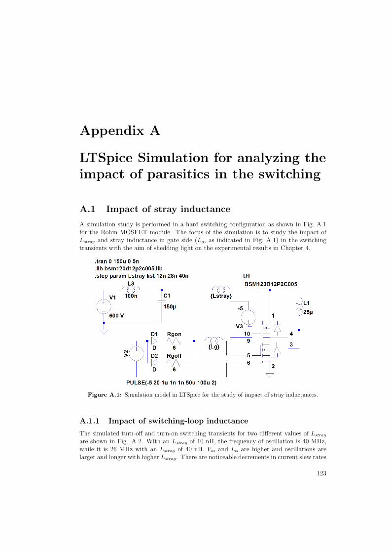
Appendix A
LTSpice Simulation for analyzing theimpact of parasitics in the switching
A.1 Impact of stray inductance
A simulation study is performed in a hard switching configuration as shown in Fig. A.1for the Rohm MOSFET module. The focus of the simulation is to study the impact ofLstray and stray inductance in gate side (Lg, as indicated in Fig. A.1) in the switchingtransients with the aim of shedding light on the experimental results in Chapter 4.
Figure A.1: Simulation model in LTSpice for the study of impact of stray inductances.
A.1.1 Impact of switching-loop inductance
The simulated turn-off and turn-on switching transients for two different values of Lstray
are shown in Fig. A.2. With an Lstray of 10 nH, the frequency of oscillation is 40 MHz,while it is 26 MHz with an Lstray of 40 nH. Vos and Ios are higher and oscillations arelarger and longer with higher Lstray. There are noticeable decrements in current slew rates
123

Chapter A. LTSpice Simulation for analyzing the impact of parasitics in the switching
time [ns]0 100 200 300 400 500 600
-20
0
20
40
60
80
100
120L
stray=10 [nH]
Id/2 [A]
Vds
/10 [V]L
stray=40 [nH]
40 [MHz]
26 [MHz]
(a) Turn-off of BSM120D12P2C005 (Rohm).
time [ns]0 100 200 300 400 500 600
-20
0
20
40
60
80
100
120L
stray=10 [nH]
Lstray
=40 [nH]
Id/2 [A]
Vds
/10 [V]
(b) Turn-on of BSM120D12P2C005 (Rohm).
Figure A.2: LTSpice simulation of turn-off and turn-on switching transients with two differentvalues of Lstray, provided Rg,ext = 6 Ω. Note that an LTSpice model of a half-bridge SiCMOSFET module, BSM120D12P2C005, is considered to investigate the impact of parasiticinductance. Clearly, the higher the Lstray, the higher the overshoot and larger and longer theoscillations.
both during turn-on and turn-off transients with larger Lstray, thereby slowing the SiCtransistors. Note that in Fig. A.2 (a), when di/dt is reduced, voltage overshoot or voltagedrop is still increased because loop inductance is increased by more than the amount di/dtis reduced.
A.1.2 Impact of gate-loop inductance
Fig. A.3 illustrates the switching transients with an Lstray of 40 nH for two different valuesof Lg. The impact of Lg on the oscillations and slew rates is not as significant as that ofLstray. Nonetheless, it slows down the device a little.
time [ns]0 100 200 300 400 500 600
-20
0
20
40
60
80
100
120
Id/2 [A]
Lg=40 [nH]
Lg=0 [nH]
Vds
/10 [V]
26 [MHz]
(a) Turn-off of BSM120D12P2C005 (Rohm).
time [ns]0 100 200 300 400 500 600
-20
0
20
40
60
80
100
120
Id/2 [A]
Vds
/10 [V]
Lg=0 [nH]
Lg=40 [nH]
(b) Turn-on of BSM120D12P2C005 (Rohm).
Figure A.3: LTSpice simulation with two Lg values; 0 nH and 40 nH, keeping Lstray = 40 nHand Rg,ext = 6 Ω.
124

Chapter A. LTSpice Simulation for analyzing the impact of parasitics in the switching
A.2 Impact of stray capacitance
A simulation model in LTSpice is used for studying the impact of Cgs, Cds, and Cgd. Anexample with Cgd connected in the model is shown in Fig. A.4. For the other cases: Cgs
and Cds variations, the capacitors are connected between the respective terminals of theMOSFET. The values are chosen as per the data sheet of the chosen modules, as listed inTable 4.5, and are considered for the case with Vds of 600 V. Although, these capacitorsshow non-linear variations with Vds, a constant value is taken into account because it issufficient for relative performance evaluation. LTSpice model of SiC MOSFET is fromWolfspeed. This section is divided in three subsections. The simulated turn-off andturn-on transients of the currents and voltages in both the gate and drain sides withdifferent Cgs, Cds, and Cgd are elaborated in Subsection A.2.1, Subsection A.2.2 andSubsection A.2.3, respectively.
PULSE(-5 20 10u 25n 25n 5u 20u 2)
V1
L3
100µ
V2
600
C1
150µ
L2
15n
R1
6.8
L1
100n
T1Cgd
C2
D1
Gate
Sour
ceD
rain
.step param Cgd list 0n 0.18n
--- C:\Users\tiwari\OneDrive\EPE3\figures\help_figs\Simulation_model_doc.asc ---
Figure A.4: Simulation model in LTSpice for the study of impact of stray capacitances. Fora case with Cgd variation, a capacitor is connected between the gate and drain terminals ofMOSFET as depicted in the model. For the other cases: Cgs and Cds variations, the capacitorsare connected between the respective terminals of the MOSFET. The values are chosen as perthe data sheet of the modules, as catalogued in Chapter 4, Table 4.5, and are taken for the casewith Vds of 600 V. Spice model of SiC MOSFET is from Wolfspeed.
A.2.1 Impact of gate-source capacitance
The simulated switching waveforms with varied Cgs are illustrated in Fig. A.5. Withhigher values of Cgs, the slew rates in gate voltages are reduced significantly, the oscilla-tions are mitigated and the delay times are prolonged, which are evident from Fig. A.5
125
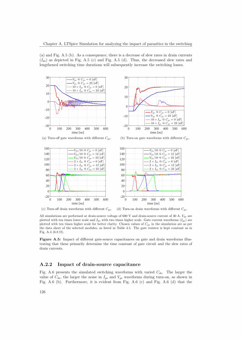
Chapter A. LTSpice Simulation for analyzing the impact of parasitics in the switching
(a) and Fig. A.5 (b). As a consequence, there is a decrease of slew rates in drain currents(Ids) as depicted in Fig. A.5 (c) and Fig. A.5 (d). Thus, the decreased slew rates andlengthened switching time durations will subsequently increase the switching losses.
time [ns]0 100 200 300 400 500 600
-30
-20
-10
0
10
20
30Vgs @ Cgs = 0 [nF]Vgs @ Cgs = 23 [nF]10× Igs @ Cgs = 0 [nF]10× Igs @ Cgs = 23 [nF]
(a) Turn-off gate waveforms with different Cgs.
time [ns]0 100 200 300 400 500 600
-20
-10
0
10
20
30
Vgs @ Cgs = 0 [nF]Vgs @ Cgs = 23 [nF]10× Igs @ Cgs = 0 [nF]10× Igs @ Cgs = 23 [nF]
(b) Turn-on gate waveforms with different Cgs.
time [ns]0 100 200 300 400 500 600
-20
0
20
40
60
80
100
120
140
160Vds/10 @ Cgs = 0 [nF]Vds/10 @ Cgs = 12 [nF]Vds/10 @ Cgs = 23 [nF]2× Ids @ Cgs = 0 [nF]2× Ids @ Cgs = 12 [nF]2× Ids @ Cgs = 23 [nF]
(c) Turn-off drain waveforms with different Cgs.
time [ns]0 100 200 300 400 500 600
-20
0
20
40
60
80
100
120
140
160Vds/10 @ Cgs = 0 [nF]Vds/10 @ Cgs = 12 [nF]Vds/10 @ Cgs = 23 [nF]2× Ids @ Cgs = 0 [nF]2× Ids @ Cgs = 12 [nF]2× Ids @ Cgs = 23 [nF]
(d) Turn-on drain waveforms with different Cgs.
All simulations are performed at drain-source voltage of 600 V and drain-source current of 30 A. Vds areplotted with ten times lower scale and Ids with two times higher scale. Gate current waveforms (Igs) areplotted with ten times higher scale for better clarity. Chosen values of Cgs in the simulation are as perthe data sheet of the selected modules, as listed in Table 4.5. The gate resistor is kept constant as inFig. A.4 (6.8 Ω).
Figure A.5: Impact of different gate-source capacitances on gate and drain waveforms illus-trating that these primarily determine the time constant of gate circuit and the slew rates ofdrain currents.
A.2.2 Impact of drain-source capacitance
Fig. A.6 presents the simulated switching waveforms with varied Cds. The larger thevalue of Cds, the larger the noise in Igs and Vgs waveforms during turn-on, as shown inFig. A.6 (b). Furthermore, it is evident from Fig. A.6 (c) and Fig. A.6 (d) that the
126

Chapter A. LTSpice Simulation for analyzing the impact of parasitics in the switching
voltage slew rates become slower and the frequency of oscillations become smaller withhigher values of Cds. In addition, the current slew rates become slightly faster leading tohigher current overshoots, as illustrated in Fig. A.6 (d).
time [ns]0 100 200 300 400 500 600
-30
-20
-10
0
10
20
30Vgs @ Cds = 0 [nF]Vgs @ Cds = 2.5 [nF]10× Igs @ Cds = 0 [nF]10× Igs @ Cds = 2.5 [nF]
(a) Turn-off gate waveforms with different Cds.
time [ns]0 100 200 300 400 500 600
-30
-20
-10
0
10
20
30
Vgs @ Cds = 0 [nF]Vgs @ Cds = 2.5 [nF]10× Igs @ Cds = 0 [nF]10× Igs @ Cds = 2.5 [nF]
(b) Turn-on gate waveforms with different Cds.
time [ns]0 100 200 300 400 500 600
-20
0
20
40
60
80
100
120
140
160Vds/10 @ Cds = 0 [nF]Vds/10 @ Cds = 1 [nF]Vds/10 @ Cds = 2.5 [nF]2× Ids @ Cds = 0 [nF]2× Ids @ Cds = 1 [nF]2× Ids @ Cds = 2.5 [nF]
(c) Turn-off drain waveforms with different Cds.
time [ns]0 100 200 300 400 500 600
-20
0
20
40
60
80
100
120
140
160Vds/10 @ Cds = 0 [nF]Vds/10 @ Cds = 1 [nF]Vds/10 @ Cds = 2.5 [nF]2× Ids @ Cds = 0 [nF]2× Ids @ Cds = 1 [nF]2× Ids @ Cds = 2.5 [nF]
(d) Turn-on drain waveforms with different Cds.
All simulations are performed at drain-source voltage of 600 V and drain-source current of 30 A. Vds areplotted with ten times lower scale and Ids with two times higher scale. Gate current waveforms (Igs)are plotted with ten times higher scale for better clarity. Chosen values of Cds in the simulation are asper the data sheet of the selected modules, as listed in Chapter 4, Table 4.5. The gate resistor is keptconstant as in Fig. A.4 (6.8 Ω).
Figure A.6: Impact of different drain-source capacitances on gate and drain waveforms illus-trating that these primarily determine the parasitic ringings and slew rates of drain voltages.
A.2.3 Impact of gate-drain capacitance
Fig. A.7 exemplifies the simulated switching waveforms with varied Cgd. It is apparentthat both the gate current and voltage waveforms oscillate when Cgd increases, which isessentially because of dv/dt related noise coupled to gate side through miller capacitor(Cgd). This noise can exceed the threshold voltage limit of SiC MOSFET and cause
127
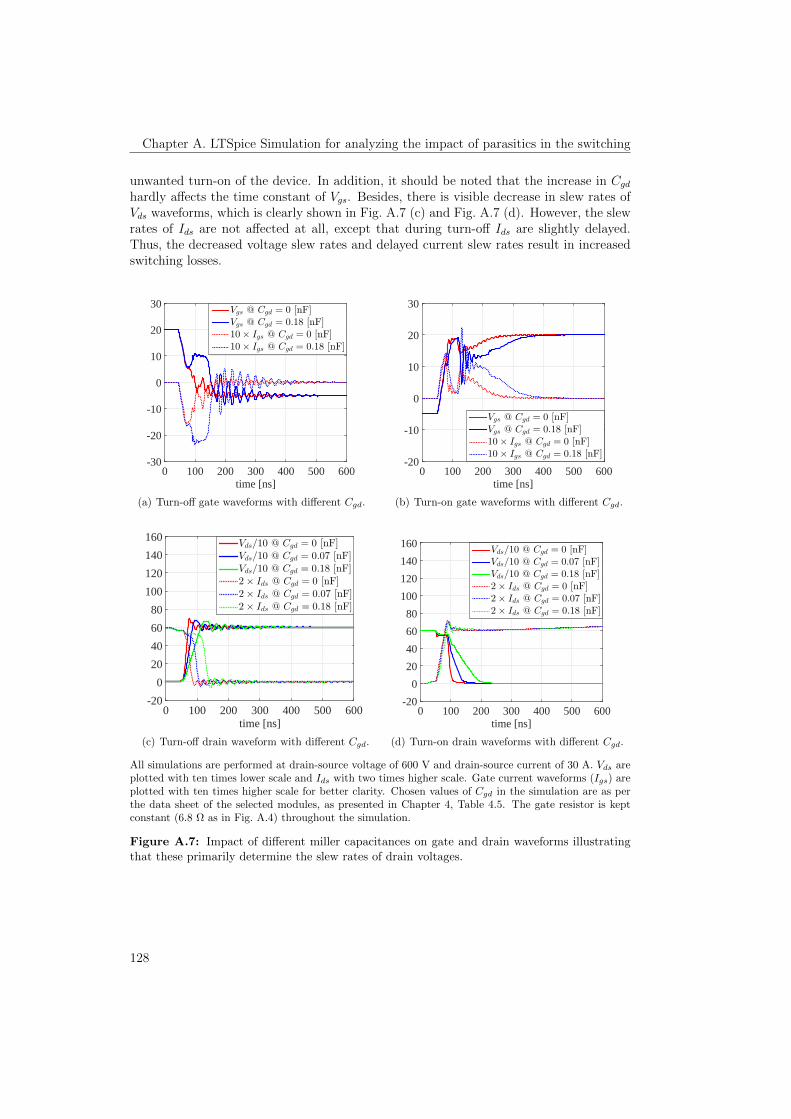
Chapter A. LTSpice Simulation for analyzing the impact of parasitics in the switching
unwanted turn-on of the device. In addition, it should be noted that the increase in Cgd
hardly affects the time constant of Vgs. Besides, there is visible decrease in slew rates ofVds waveforms, which is clearly shown in Fig. A.7 (c) and Fig. A.7 (d). However, the slewrates of Ids are not affected at all, except that during turn-off Ids are slightly delayed.Thus, the decreased voltage slew rates and delayed current slew rates result in increasedswitching losses.
time [ns]0 100 200 300 400 500 600
-30
-20
-10
0
10
20
30Vgs @ Cgd = 0 [nF]Vgs @ Cgd = 0.18 [nF]10× Igs @ Cgd = 0 [nF]10× Igs @ Cgd = 0.18 [nF]
(a) Turn-off gate waveforms with different Cgd.
time [ns]0 100 200 300 400 500 600
-20
-10
0
10
20
30
Vgs @ Cgd = 0 [nF]Vgs @ Cgd = 0.18 [nF]10× Igs @ Cgd = 0 [nF]10× Igs @ Cgd = 0.18 [nF]
(b) Turn-on gate waveforms with different Cgd.
time [ns]0 100 200 300 400 500 600
-20
0
20
40
60
80
100
120
140
160Vds/10 @ Cgd = 0 [nF]Vds/10 @ Cgd = 0.07 [nF]Vds/10 @ Cgd = 0.18 [nF]2× Ids @ Cgd = 0 [nF]2× Ids @ Cgd = 0.07 [nF]2× Ids @ Cgd = 0.18 [nF]
(c) Turn-off drain waveform with different Cgd.
time [ns]0 100 200 300 400 500 600
-20
0
20
40
60
80
100
120
140
160Vds/10 @ Cgd = 0 [nF]Vds/10 @ Cgd = 0.07 [nF]Vds/10 @ Cgd = 0.18 [nF]2× Ids @ Cgd = 0 [nF]2× Ids @ Cgd = 0.07 [nF]2× Ids @ Cgd = 0.18 [nF]
(d) Turn-on drain waveforms with different Cgd.
All simulations are performed at drain-source voltage of 600 V and drain-source current of 30 A. Vds areplotted with ten times lower scale and Ids with two times higher scale. Gate current waveforms (Igs) areplotted with ten times higher scale for better clarity. Chosen values of Cgd in the simulation are as perthe data sheet of the selected modules, as presented in Chapter 4, Table 4.5. The gate resistor is keptconstant (6.8 Ω as in Fig. A.4) throughout the simulation.
Figure A.7: Impact of different miller capacitances on gate and drain waveforms illustratingthat these primarily determine the slew rates of drain voltages.
128

Appendix B
3D FEM simulation for lowinductive circuit designs
B.1 Modelling of busbar in Ansys Q3D extractor
In this section, the fundamentals of modelling of busbar in Ansys Q3D extractor aredescribed. A busbar for single-phase, half-bridge converter is presented as an example toillustrate the modelling procedure in the software. In order to model the busbar whichfunctions as two conductors carrying the current in opposite directions, overall, threesteps have to be followed.
First, a 3D geometric structure of the busbar should be built, i.e., dimensions ofthe busbar are taken as input parameters. Additionally, the material characteristics foreach object should be specified. Second, as the stray inductance and resistance dependon the current conduction loop, the current direction, both source and sink, for eachconduction path must be specified. This step is further explained in the following substeps. Initially, the start face in the first conductor is assigned as source 1 and the endface as sink 1. Thereafter, the start face is assigned as sink 2 and the end face as source 2in the second conductor. Fig. B.1 further clarifies which terminals are excited as sourcesand which as sinks. Third, the two busbars should be connected in series so that theloop inductance can be calculated. For that, the sink 1 and the source 2 are assigned asin series connections. These steps model the two plates as a transmission line where thepositive and negative plates are just on top of each other. The software generates thenecessary impedance matrices which can be represented by the lumped element circuitmodel as in Fig. B.2, where L11 and L22, C11 and C22, and R11 and R22 are the self-inductances, capacitances and resistances respectively. Likewise, L12 and L21, C12 andC21 are the mutual-inductances and capacitances. As the two busbars are modelled ascurrent carrying conductors in opposite directions, the loop inductance is also generatedwhich follows (B.1). It should be noted that ESL of capacitor is not considered in thecalculation.
Lloop = L11 + L22 − 2L12 (B.1)
A method to achieve lower inductance is the paralleling of many connections, that iswhy capacitors with several pins are chosen. The opposite pins of the bypass capacitorare separated by 24 mm, and the height is 4 mm. These terminations effectively make
129

Chapter B. 3D FEM simulation for low inductive circuit designs
Figure B.1: Picture illustrating a standard module package with screw holes at 28 mm sepa-ration (left), a film capacitor with six pins where the opposite pins are at a distance of 24 mm(right) and a busbar connecting these two components (middle). w/l ratio of the busbar in boththe capacitor and module sides are kept at 1 to achieve low inductance.
Source 1
Sink 2
Sink 1
Source 2
L11/2R11/2 R11/2
C10
L22/2R22/2
C12
C20
L11/2
L11/2R22/2
L12/2 L12/2
Note: The variables used in Fig. B.2 are: R11 and R22, resistances; L11 and L22, self-inductances; L12
and L21, mutual-inductances; C11 and C22, self-capacitances of each conductors (not shown in the model);C12 and C21, mutual-capacitances, C10 and C20, capacitances between the conductor and ground.
Figure B.2: Lumped element circuit model of busbar.
the corresponding part of the busbar coplanar. The screw terminations of the modulesare 28 mm apart, however, the DC-link busbar is made such that there is some overlap(12 mm) in the termination part. This makes the effective distance between the termina-tions smaller. The self- and mutual-inductance, as in Fig. B.2, are L11 = 30.7 nH, L22 =19.31 nH, and L12 = L21 = 18 nH respectively, and the loop inductance Lloop is 14 nH.The difference in self-inductance between the two opposite plates is also the indicationthat the capacitor termination is coplanar.
Furthermore, the distribution of current density in the busbar from Ansys Q3D isexemplified in Fig. B.3, where the red color shading indicates the higher current density.The major parts of the current are concentrated around the holes, sharp corners and edges,therefore, it is essential to minimize the number of holes and make the edges round, whichresults in an increase of surface area. These considerations will eventually minimize thestray inductance. In addition, the part of the busbar which has not contributed in
130

Chapter B. 3D FEM simulation for low inductive circuit designs
the current flow can be eliminated. Consequently, a more compact and a lightweightconverter is possible. The excluded parts and the round edges are depicted in Fig. B.3 (b).
Load terminal
hole for screw
Clearance hole
a)
b)
Figure B.3: Distribution of current density in the busbar from Ansys Q3D, red color shadingindicates higher current density. Most of the current is concentrated towards the capacitor pinsand the load terminals as they are identified to be coplanar structures. The part of the busbarthat has not contributed in the current flow can be eliminated and the sharp edges can be maderound, as shown in Fig. (b).
131
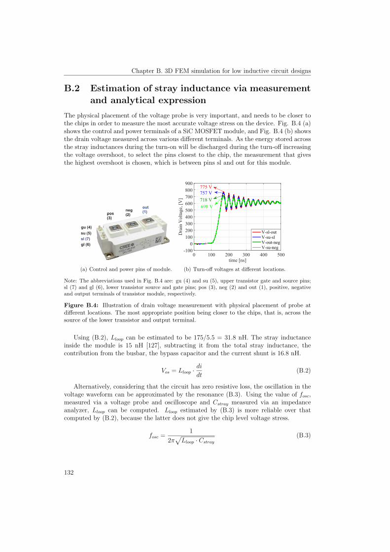
Chapter B. 3D FEM simulation for low inductive circuit designs
B.2 Estimation of stray inductance via measurement
and analytical expression
The physical placement of the voltage probe is very important, and needs to be closer tothe chips in order to measure the most accurate voltage stress on the device. Fig. B.4 (a)shows the control and power terminals of a SiC MOSFET module, and Fig. B.4 (b) showsthe drain voltage measured across various different terminals. As the energy stored acrossthe stray inductances during the turn-on will be discharged during the turn-off increasingthe voltage overshoot, to select the pins closest to the chip, the measurement that givesthe highest overshoot is chosen, which is between pins sl and out for this module.
pos(3)
neg (2)
out(1)
gu (4)
su (5)
sl (7)
gl (6)
pos (2)po(3)
(2)
(a) Control and power pins of module.
time [ns]0 100 200 300 400 500
Dra
in V
olt
age,
[V
]
-100
0
100
200
300
400
500
600
700
800
900
V-sl-out
V-su-sl
V-out-neg
V-su-neg
698 V
757 V
775 V
718 V
(b) Turn-off voltages at different locations.
Note: The abbreviations used in Fig. B.4 are: gu (4) and su (5), upper transistor gate and source pins;sl (7) and gl (6), lower transistor source and gate pins; pos (3), neg (2) and out (1), positive, negativeand output terminals of transistor module, respectively.
Figure B.4: Illustration of drain voltage measurement with physical placement of probe atdifferent locations. The most appropriate position being closer to the chips, that is, across thesource of the lower transistor and output terminal.
Using (B.2), Lloop can be estimated to be 175/5.5 = 31.8 nH. The stray inductanceinside the module is 15 nH [127], subtracting it from the total stray inductance, thecontribution from the busbar, the bypass capacitor and the current shunt is 16.8 nH.
Vos = Lloop ·di
dt(B.2)
Alternatively, considering that the circuit has zero resistive loss, the oscillation in thevoltage waveform can be approximated by the resonance (B.3). Using the value of fosc,measured via a voltage probe and oscilloscope and Cstray measured via an impedanceanalyzer, Lloop can be computed. Lloop estimated by (B.3) is more reliable over thatcomputed by (B.2), because the latter does not give the chip level voltage stress.
fosc =1
2π√Lloop · Cstray
(B.3)
132

Appendix C
Fundamental information forChapter 6
C.1 Equations for passive component sizing
LB =1
∆iL·v2s,min
Pout
·
(1−√
2 · vs,min
vout
)· 1
fsw(C.1)
Cout =2 · Pout · tholdv2s,min − v2out,min
,=Pout
2 · π · fline ·∆vout · vout(C.2)
The higher value of Cout is considered to be the output capacitor size for the design.
Note: The variables used in (C.1) and (C.2) are: LB , inductance of boost inductor; ∆iL, boost
inductor ripple current; vs,min, minimum input voltage; Pout, output power; vout, output voltage; fsw,
switching frequency; vout,min, minimum output voltage; thold, hold-up-time; ∆vout, output voltage ripple;
and fline, lines/mains frequency.
C.2 Equations for conduction loss calculation
Pcond(rectifier) = 2× (I2L,rms ×Rd + IL,avg × VFO)
Pcond(inductor) = I2L,rms ×DCRPcond(capacitor) = I2c,rms × ESR
Pcond(MOSFET ) = I2ds,rms ×RDS,on
Pcond(diode) = I2d,rms ×Rd + Id,avg × VFO
(C.3)
Note: The variables used in (C.3) are: Pcond, conduction loss; IL,rms and IL,avg, rms and average
current of diode rectifier; Id,rms and Id,avg, rms and average current of boost diode; Ids,rms, rms current
of MOSFET; and Ic,rms, rms current of output capacitor.
133

Chapter C. Fundamental information for Chapter 6
C.3 A complete schematic diagram and component
layout of PFC rectifier (two-layer board)
Tw
o stag
e
EM
I filter
Gate d
river
Bo
ost in
du
ctor
SiC
M
OS
FE
T S
iC d
iod
e
Co
ntro
l
circuit
+ 4
00
V
Ou
tpu
t
capacito
r
Pro
vid
es
inru
sh cu
rrent
limitatio
ns
Byp
ass dio
de
PF
C
con
troller
UC
C28
18
0
Z1 an
d Z
2 pro
vid
es gate
ov
ervo
ltage p
rotectio
n
D6 an
d D
7
limits th
e
zener d
iod
e
capacitan
ces
+1
8 V
-4 V
Brid
ge
rectifier
L3
-A
attenu
ates
DM
EM
I
L1
-A –
L2
-A
attenu
ates
CM
EM
I
Figure C.1: A complete schematic diagram of the PFC rectifier prototype board.
134

Chapter C. Fundamental information for Chapter 6
Tw
o stag
e
EM
I filter
Driv
er and
con
trol circu
its
Ou
tpu
t
capacito
r B
oo
st
inducto
r
PF
C co
ntro
ller
UC
C28180D
Gate
driv
er IC
UC
C27
5
38D
BV
Gro
und
plan
e
Gate d
rive
track
Balan
ced
switch
ing
conducto
rs
Hig
h v
oltag
e
switch
ing
track
Figure C.2: A complete component layout and routing of the PFC rectifier prototype board(two-layer board).
135

Chapter C. Fundamental information for Chapter 6
136

Appendix D
An insight into close-to-losslessswitching enabled by SiC MOSFET
SiC offers lower input and output capacitances compared to their Si counterparts, therebyposing an inherent potential to reduce the dynamic power loss, provided the low inductiveswitching loop is ensured. Therefore, for fully unleashing the fast switching benefits of SiCMOSFET, a symmetrical and a low inductive design of switching loop for a single-phase,full-bridge inverter is addressed in this chapter. Employing a 3D FEM model, the insightinto the physical behavior of the current flow in a switching loop is identified. Essentiallyfocusing on the proper orientation and distribution of the DC-clamping capacitors andSiC MOSFETs, this work demonstrates that the parasitic inductance of 3 nH includingthe bussing structure and connections can be achieved. A 20 kW series-resonant inverterswitched at 2 MHz is simulated via an LTSpice. The model includes the device parasiticsof the DC-clamping capacitors and the third generation SiC MOSFET from Wolfspeed,C3M0065090J, and circuit parasitics of 3 nH extracted from FEM simulation. At a peakload current, the inverter yielded a voltage overshoot of less than 11% of the DC-linkvoltage. This is the reported lowest value of loop inductance employing discrete SiCMOSFET with TO-263-7 package. In addition, explaining the detailed switching process,this work provides insight into how a close-to-lossless switching can be achieved. Theconcept is verified via simulation results in a 20 kW SiC-based resonant inverter.
D.1 Introduction
In a sine wave current switched inverter, such as LLC resonant for induction heatingapplications, there are predominantly two reasons for designing the low inductive currentcommutation loop. First, to ensure safety, particularly during failure; i.e., in such aninverter, often, a short circuit is incurred by the shorting of coil and the work piece(which is supposed to be contactless), and the inverter needs to be turned off. With lowinductive switching loop, hard turn-off will be even safer, as it does not create too highover voltage at chip level, and there will be no need for soft turn-off and thereby a simplerdriver can be used. Second, dynamic loss can be reduced because stray inductance is oneof the parameters hindering the device from switching fast to its highest potential.
Therefore, at first, a low inductive circuit layout is designed via Ansys Q3D, thebussing structure and connections of components resulted in a loop inductance of 3 nH.This is principally achieved by the proper selection, orientation and distribution of the DC-
137

Chapter D. An insight into close-to-lossless switching enabled by SiC MOSFET
clamping capacitors and SiC MOSFET, and is discussed in Section D.2. Thereafter, thesimulated parasitic inductance value from Q3D, and device parasitics of the DC-clampingcapacitors are used as inputs in LTSpice tool for simulating the complete inverter setup asin an experimental arrangements in Section D.3, the primary goal of which is to evaluatethe voltage overshoot when switching at peak of sinusoidal load current. Note that theSpice model of third generation SiC MOSFET from Wolfspeed, C3M0065090J, includesthe parasitics in it. Furthermore, an optimal operating condition is investigated such thatSiC MOSFETs operate close to zero switching loss.
D.2 Design of low inductive layout via 3D FEM sim-
ulation in Ansys Q3D
T4
T3
T2
T1 D1
D2
D3
D4
DCC
Output A Output B
outVout
I
14T
I
14T
I
(a) Current routing through transistors T1 and T4.
T4
T3
T2
T1 D1
D2
D3
D4
DCC
Output A Output B
outVout
I
23D
I
23D
I
(b) Current routing through diodes D2 and D3.
Figure D.1: (a) and (b) Exemplification of the current flow during the positive polarity of loadcurrent. During the negative polarity of the load current, the opposite transistors T2 and T3and the diodes D1 and D4 function.
Before delving into the design of symmetrical low inductive layout, it is importantto discuss the current commutation loops in a single-phase, full-bridge resonant inverter.Fig. D.1 shows the current flow during the positive polarity of load current. During thenegative polarity of the load current, the complementary transistors T2 and T3 and thediodes D1 and D4 operate, which is not shown here. For equal output current and voltage,each current commutation loop should have equal stray inductances, that is, it should besymmetrical. Therefore, the DC-clamping capacitors are mounted in the middle part inFig. D.1.
By specifying the input parameters, such as 3D geometry, material properties (suchas copper for busbar and Kapton for dielectric), and the desired output, an Ansys Q3Dextractor generates the necessary impedance matrices which can be represented by thelumped element circuit model. Fig. D.2 (a) shows a complete 3D FEM model of the
138

Chapter D. An insight into close-to-lossless switching enabled by SiC MOSFET
components layout in such an inverter, where the DC-clamping capacitors are evenlydistributed immediately adjacent to the four paralleled discrete SiC MOSFETs. Severalfactors which involve low loop inductance are considered in this design. For instance,Ceralink capacitors are chosen as they have small height, low stray inductances and highcurrent capacity; SiC MOSFETs with TO-263-7 packages have low height, separate powerand source returns, where five pins are accounted as power return and one as sourcereturns; and copper plates are assembled in a transmission line like layout such thatwidth to length ratio of the current path is kept greater than 1. Fig. D.2 (b) illustratesthe FEM simulation of a half-symmetry of the full model as shown in Fig. D.2 (a), theQ3D extracted loop inductance of which is 3 nH. Highly stressed parts are indicated bydeep red color shading in the top and back view of the model.
(a) Total geometrical model of a single-phase, full-bridge inverter.
Top view
Back view
(b) Ansys Q3D simulation of a half-symmetry model.
Figure D.2: (a) A complete components layout in a single-phase, full-bridge inverter, includingDC-clamping capacitors, TO-263-7 packaged SiC MOSFETs, copper plates and insulation layer.Width to length ratio of the current path is maintained greater than unity in each of the half-bridges in order to acquire minimum loop inductance. Note that the thickness of copper plateis 1 mm. (b) Illustration of FEM simulation of a half-symmetry model employing Ansys Q3D.Deep red color shading in the current density plot indicates the highly stressed parts in the topand back view of the model and the loop inductance shared by bussing structure and componentconnections is computed to be 3 nH.
139

Chapter D. An insight into close-to-lossless switching enabled by SiC MOSFET
Figure D.3: Illustration of a complete simulation model of a 20 kW series-resonant inverter,switched at a frequency of 2 MHz. Note that these spice models also include package inductance.
140
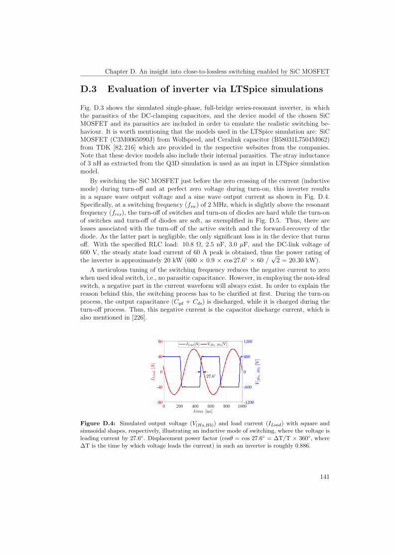
Chapter D. An insight into close-to-lossless switching enabled by SiC MOSFET
D.3 Evaluation of inverter via LTSpice simulations
Fig. D.3 shows the simulated single-phase, full-bridge series-resonant inverter, in whichthe parasitics of the DC-clamping capacitors, and the device model of the chosen SiCMOSFET and its parasitics are included in order to emulate the realistic switching be-haviour. It is worth mentioning that the models used in the LTSpice simulation are: SiCMOSFET (C3M0065090J) from Wolfspeed, and Ceralink capacitor (B58031L7504M062)from TDK [82, 216] which are provided in the respective websites from the companies.Note that these device models also include their internal parasitics. The stray inductanceof 3 nH as extracted from the Q3D simulation is used as an input in LTSpice simulationmodel.
By switching the SiC MOSFET just before the zero crossing of the current (inductivemode) during turn-off and at perfect zero voltage during turn-on, this inverter resultsin a square wave output voltage and a sine wave output current as shown in Fig. D.4.Specifically, at a switching frequency (fsw) of 2 MHz, which is slightly above the resonantfrequency (fres), the turn-off of switches and turn-on of diodes are hard while the turn-onof switches and turn-off of diodes are soft, as exemplified in Fig. D.5. Thus, there arelosses associated with the turn-off of the active switch and the forward-recovery of thediode. As the latter part is negligible, the only significant loss is in the device that turnsoff. With the specified RLC load: 10.8 Ω, 2.5 nF, 3.0 µF, and the DC-link voltage of600 V, the steady state load current of 60 A peak is obtained, thus the power rating ofthe inverter is approximately 20 kW (600 × 0.9 × cos 27.6 × 60 /
√2 = 20.30 kW).
A meticulous tuning of the switching frequency reduces the negative current to zerowhen used ideal switch, i.e., no parasitic capacitance. However, in employing the non-idealswitch, a negative part in the current waveform will always exist. In order to explain thereason behind this, the switching process has to be clarified at first. During the turn-onprocess, the output capacitance (Cgd + Cds) is discharged, while it is charged during theturn-off process. Thus, this negative current is the capacitor discharge current, which isalso mentioned in [226].
0 200 400 600 800 1000-80
-40
0
40
80
-1200
-600
0
600
1200
Figure D.4: Simulated output voltage (V(Ha,Hb)) and load current (ILoad) with square andsinusoidal shapes, respectively, illustrating an inductive mode of switching, where the voltage isleading current by 27.6. Displacement power factor (cosθ = cos 27.6 = ∆T/T × 360, where∆T is the time by which voltage leads the current) in such an inverter is roughly 0.886.
141

Chapter D. An insight into close-to-lossless switching enabled by SiC MOSFET
0 200 400 600 800 1000-10
0
10
20
30
40
-200
0
200
400
600
800
(a) Voltage and current of the switch U1.
0 200 400 600 800 1000-10
0
10
20
30
40
-200
0
200
400
600
800
(b) Voltage and current of the switch U15.
Figure D.5: (a) and (b) Switching voltages and currents of the complementary transistors (forinstance, U1 and U15), illustrating an inductive mode of switching in a series-resonant inverter,where the switching frequency is slightly above the resonant frequency (given by RLC load).
D.3.1 Analysis of voltage overshoot when switched at 8 A
Fig. D.6 (a) and (b) show the turn-off and turn-on transients, respectively, at the switchingcurrent of 8 A and the DC-link voltage of 600 V. Apparently, the voltage overshoot is <3% of the DC-link voltage. In a classical electrical loss measurement method, the turn-onloss is underestimated and the turn-off loss is overestimated by the amount of energystored or discharged in the Coss. Provided the upper and lower switches are identical, thelosses associated with the charging and discharging of the Coss are equal, the summationof the losses calculated by the classical approach will give the total actual power loss inthe switching device.
0 30 60 90 120 150-4
0
4
8
12
16
-200
0
200
400
600
800
BA
(a) Time domain plot of turn-off switching tran-sients. Integrating the power curve from A toB, turn-off energy loss is simulated to be 14 µJat the switching current of 8 A.
0 30 60 90 120 150-4
0
4
8
12
16
-200
0
200
400
600
800
BA
(b) Time domain plot of turn-on switching tran-sients. Integrating the power curve from A toB, turn-off energy loss is simulated to be 12 µJat the switching current of 8 A.
Figure D.6: (a) Turn-off switching transient when switched at 8 A, the voltage overshoot is< 3% of DC-link voltage. (b) Turn-on switching transients showing the negative current whichis associated with the discharging of the MOSFET output capacitance.
142

Chapter D. An insight into close-to-lossless switching enabled by SiC MOSFET
In the zero voltage switching technique, switches have soft turn-on and diodes havesoft turn-off, that is, there is no recovery current. The negative part of the current is, asmentioned earlier, thus the capacitor discharge current. Multiplying the voltage acrossthe switch and the current through it, power loss in the switch is found. Integrating thepower over a defined interval of time, as shown in Fig. D.6 (a) and (b), the energy loss iscomputed. Provided the loss during the turn-on is close to the loss during the turn-off, theinverter works close-to-lossless switching. For instance, in the simulation, turn-on energyloss was found to be 12 µJ and the turn-off energy loss to be 14 µJ. A zoomed-in view ofFig. D.6 (a) and (b) are shown in Fig. D.7 (a) and (b), respectively. Obviously, duringthe turn-off, Coss is charged and during the turn-on, it is discharged. Examining closely,a drop of 50% in the initial switching current (8 A) entails close to zero turn-off loss.
0 10 20 30 40 50 60-4
0
4
8
12
16
-200
0
200
400
600
800
50 %
(a) Turn-off transients. Initial 50% drop in cur-rent after turn-off starts (from 8 A to 4 A) isfast, the di/dt of which is 0.47 A/ns, whichis more visible with 30 ns/div of time scale inFig. D.6 (a).
0 10 20 30 40 50 60-4
0
4
8
12
16
-200
0
200
400
600
800
(b) Turn-on transients.
Figure D.7: (a) Turn-off transients showing different dv/dt at various points. Initially, Coss islarge at low voltage, so dv/dt1 is low, then, dv/dt2 is high, and finally, dv/dt3 is low. (b) Turn-ontransients also show similar characteristics as in (a). During the turn-off, Coss is charged andduring the turn-on, it is discharged.
D.3.2 Analysis of voltage overshoot when switched at 15 A
Fig. D.8 (a) and (b) show the turn-off and turn-on transients, respectively, at the switchingcurrent of 15 A (peak of sinusoidal load current) and the DC-link voltage of 600 V.Apparently, the voltage overshoot is < 11% of the DC-link voltage. Note that di/dt is2.85 A/ns and dv/dt is 89.5 V/ns, and the frequency of oscillations is 128 MHz. Of specialnote is that as current increases, dv/dt and di/dt increase and as a consequencethe oscillations are pronounced even though the loop inductance is 5 nH.Following a similar approach as seen in Subsection D.3.1, turn-on and turn-off energylosses are computed and found to be 11 µJ and 14.6 µJ, respectively, leading to the actualswitching loss of 3.6 µJ (14.6 - 11 = 3.6 µJ). It should be pointed out that this case isalso close to zero switching loss as the specific energy loss is 0.24 µJ/A (= 3.6 µJ/15 A).
143

Chapter D. An insight into close-to-lossless switching enabled by SiC MOSFET
0 30 60 90 120 150-5
0
5
10
15
20
-200
0
200
400
600
800
(a) Time domain plot of turn-off switching tran-sients. Turn-off energy loss is simulated to be14.6 µJ at the switching current of 15 A and theDC-link voltage of 600 V.
0 30 60 90 120 150-20
-12
-4
4
12
20
-200
0
200
400
600
800
(b) Time domain plot of turn-on switching tran-sients. Turn-on energy loss is simulated to be11 µJ at the switching current of 15 A and theDC-link voltage of 600 V.
Figure D.8: (a) and (b) Turn-off and turn-on switching transients when switched at peak ofsinusoidal load current (15 A), the voltage overshoot is < 11% of DC-link voltage. The totalswitching loss is 3.6 µJ (14.6 - 11 = 3.6 µJ) because the turn-off loss is positive and turn-on lossis negative.
D.3.3 Conclusion
As SiC MOSFETs can be switched with very high dv/dt; i.e., the current can be switchedoff instantly (close to ideal switch). In the simulation with ideal switch, the current doesnot appear in the negative direction during turn-on, but with real switch (with Coss),it appears in the negative direction as well, which is the Coss discharging current in theupper switch. If this power area in the negative side is maintained equal while turningoff the lower transistor (meaning the area in the positive direction is just the energy thatcharges the capacitor), then close-to-lossless switching can be achieved.
144

Bibliography
[1] N. Mohan, T. M. Undeland, and W. P. Robbins, Power Electronics: Converters,Applications, and Design. New York: John Wiley & Sons, 1995.
[2] F. Wang, Z. Zhang, T. Ericsen, R. Raju, R. Burgos, and D. Boroyevich, “Advancesin Power Conversion and Drives for Shipboard Systems,” Proceedings of the IEEE,vol. 103, no. 12, pp. 2285–2311, Dec. 2015.
[3] J. Stark, “380V dc power: Shaping the future of data center energy efficiency,”Data Center Knowledge, June 2015.
[4] E. Prem, “Electronics enabling efficient energy usage—results from the E4Uproject,” E4U, Tech. Rep., Dec. 2009. [Online]. Available: www.e4efficiency.eu
[5] ABB Communications, “Power electronics: the hidden technology that makes themodern world run,” Press Release, May 2013.
[6] J. Rabkowski, D. Peftitsis, and H. Nee, “Silicon Carbide Power Transistors: A NewEra in Power Electronics Is Initiated,” IEEE Industrial Electronics Magazine, vol. 6,no. 2, pp. 17–26, June 2012.
[7] B. K. Bose, “Power Electronics, Smart Grid, and Renewable Energy Systems,”Proceedings of the IEEE, vol. 105, no. 11, pp. 2011–2018, Nov. 2017.
[8] O. Kreutzer, B. Eckardt, and M. Mrz, “Unidirectional fast switching non-isolated100 kW fuel cell boost converter,” in 2014 16th European Conference on PowerElectronics and Applications, Aug. 2014, pp. 1–10.
[9] P. G. Neudeck, R. S. Okojie, and L.-Y. Chen, “High-temperature electronics–a rolefor wide bandgap semiconductors?” Proceedings of the IEEE, vol. 90, no. 6, pp.1065–1076, June 2002.
[10] R. Abebe, G. Vakil, G. Lo Calzo, T. Cox, S. Lambert, M. Johnson, C. Gerada,and B. Mecrow, “Integrated motor drives: state of the art and future trends,” IETElectric Power Applications, vol. 10, no. 8, pp. 757–771, 2016.
[11] J. Hornberger, A. B. Lostetter, K. J. Olejniczak, T. McNutt, S. M. Lal, and A. Man-tooth, “Silicon-carbide (SiC) semiconductor power electronics for extreme high-temperature environments,” in 2004 IEEE Aerospace Conference Proceedings (IEEECat. No.04TH8720), vol. 4, Mar. 2004, pp. 2538–2555 Vol.4.
145
BIBLIOGRAPHY
[12] R. W. Johnson, J. L. Evans, P. Jacobsen, J. R. Thompson, and M. Christo-pher, “The changing automotive environment: high-temperature electronics,” IEEETransactions on Electronics Packaging Manufacturing, vol. 27, no. 3, pp. 164–176,July 2004.
[13] P. Hedelin, P. Knagenhjelm, and M. Skoglund, “Silicon Carbide High TemperatureElectronics - Is This Rocket Science?” in Future Trends in Microelectronics : fron-tiers and innovations, W. B. Kleijn and K. K. Paliwal, Eds. Hoboken, N.J.: Wiley,2013, ch. 7, pp. 102–109.
[14] J. Milln, P. Godignon, X. Perpi, A. Prez-Toms, and J. Rebollo, “A Survey of WideBandgap Power Semiconductor Devices,” IEEE Transactions on Power Electronics,vol. 29, no. 5, pp. 2155–2163, May 2014.
[15] S. Tiwari, J. K. Langelid, T. M. Undeland, and O.-M. Midtgard, “Merits of SiCMOSFETs for high-frequency soft-switched converters, measurement verificationsby both electrical and calorimetric methods,” EPE Journal, vol. 0, no. 0, pp. 1–11,Feb. 2019.
[16] K. Vechalapu, S. Bhattacharya, E. V. Brunt, S. Ryu, D. Grider, and J. W. Palmour,“Comparative Evaluation of 15-kV SiC MOSFET and 15-kV SiC IGBT for Medium-Voltage Converter Under the Same dv/dt Conditions,” IEEE Journal of Emergingand Selected Topics in Power Electronics, vol. 5, no. 1, pp. 469–489, Mar. 2017.
[17] S. Tiwari, O.-M. Midtgard, and T. M. Undeland, “Experimental performance eval-uation of two commercially available, 1.2 kV half-bridge SiC MOSFET modules,” inIECON 2016 - 42nd Annual Conference of the IEEE Industrial Electronics Society,Oct. 2016, pp. 1106–1111.
[18] S. Tiwari, O.-M. Midtgard, and T. M. Undeland, “Comparative evaluation of acommercially available 1.2 kV SiC MOSFET module and a 1.2 kV Si IGBT mod-ule,” in IECON 2016 - 42nd Annual Conference of the IEEE Industrial ElectronicsSociety, Oct. 2016, pp. 1093–1098.
[19] S. Tiwari, I. Abuishmais, J. K. Langelid, R. Lund, O.-M. Midtgard, and T. M.Undeland, “Characterization of Body Diodes in the-State-of-the-Art SiC FETs-areThey Good Enough as Freewheeling Diodes?” in 2018 20th European Conferenceon Power Electronics and Applications (EPE’18 ECCE Europe), Sept. 2018, pp.P.1–P.10.
[20] H. Zhang and L. M. Tolbert, “Efficiency Impact of Silicon Carbide Power Electronicsfor Modern Wind Turbine Full Scale Frequency Converter,” IEEE Transactions onIndustrial Electronics, vol. 58, no. 1, pp. 21–28, Jan. 2011.
[21] Z. Zhang, F. Wang, L. M. Tolbert, B. J. Blalock, and D. J. Costinett, “Evaluationof Switching Performance of SiC Devices in PWM Inverter-Fed Induction MotorDrives,” IEEE Transactions on Power Electronics, vol. 30, no. 10, pp. 5701–5711,Oct. 2015.
146

BIBLIOGRAPHY
[22] S. Tiwari, T. Undeland, O.-M. Midtgard, and R. Nilsen, “SiC MOSFETs for Off-shore Wind Applications,” Journal of Physics: Conference Series, vol. 1104, no. 1,p. 012032, 2018.
[23] EFD Induction AS, “Introducing SiC transistors,” Press Release, Mar. 2018.
[24] S. Tiwari, S. Basu, T. Undeland, and O.-M. Midtgard, “Efficiency and ConductedEMI evaluation of a single-phase power factor correction boost converter using state-of-the-art SiC MOSFET and SiC diode,” IEEE Transactions on Industry Applica-tions, pp. 1–1, 2019.
[25] P. Beckedahl, S. Buetow, A. Maul, M. Roeblitz, and M. Spang, “400 A, 1200 V SiCpower module with 1nH commutation inductance,” in CIPS 2016; 9th InternationalConference on Integrated Power Electronics Systems, Mar. 2016, pp. 1–6.
[26] M. Frisch and T. Ern, “Power module with additional low inductive current path,”in 2010 6th International Conference on Integrated Power Electronics Systems, Mar.2010, pp. 1–6.
[27] M. C. Caponet, F. Profumo, R. W. De Doncker, and A. Tenconi, “Low stray in-ductance bus bar design and construction for good EMC performance in powerelectronic circuits,” IEEE Transactions on Power Electronics, vol. 17, no. 2, pp.225–231, Mar. 2002.
[28] J. Guichon, J. Aime, J. Schanen, C. Martin, J. Roudet, E. Clavel, M. Arpilliere,R. Pasterczyk, and Y. L. Floch, “Busbar design: How to spare nanohenries ?” inConference Record of the 2006 IEEE Industry Applications Conference Forty-FirstIAS Annual Meeting, vol. 4, Oct. 2006, pp. 1865–1869.
[29] S. Tiwari, O.-M. Midtgard, and T. M. Undeland, “Design of low inductive busbarfor fast switching SiC modules verified by 3D FEM calculations and laboratorymeasurements,” in 2016 IEEE 17th Workshop on Control and Modeling for PowerElectronics (COMPEL), June 2016, pp. 1–8.
[30] S. Tiwari, T. M. Undeland, and O.-M. Midtgard, “An insight into geometry andorientation of capacitors for high-speed power circuits,” in 2018 IEEE 19th Work-shop on Control and Modeling for Power Electronics (COMPEL), June 2018, pp.1–8.
[31] N. Ikeda, Y. Niiyama, H. Kambayashi, Y. Sato, T. Nomura, S. Kato, and S. Yoshida,“GaN Power Transistors on Si Substrates for Switching Applications,” Proceedingsof the IEEE, vol. 98, no. 7, pp. 1151–1161, July 2010.
[32] C. R. Eddy, P. Wu, I. Zwieback, B. L. VanMil, R. L. Myers-Ward, J. L. Tedesco,A. E. Souzis, and D. K. Gaskill, “Microhardness of 6H- and 4H-SiC Substrates,” inSilicon Carbide and Related Materials 2008, ser. Materials Science Forum, vol. 615.Trans Tech Publications, 7 2009, pp. 323–326.
[33] “Gallium nitride (gan) versus silicon carbide (sic) in the high frequency (rf) andpower switching applications,” White Paper, Microsemi PPG., 2014.
147

BIBLIOGRAPHY
[34] J. W. Palmour, “Silicon carbide power device development for industrial markets,”in 2014 IEEE International Electron Devices Meeting, Dec. 2014, pp. 1.1.1–1.1.8.
[35] B. J. Baliga, Fundamentals of Power Semiconductor Devices. Boston, MA: SpringerUS, 2008.
[36] S. Madhusoodhanan, A. Tripathi, D. Patel, K. Mainali, A. Kadavelugu, S. Hazra,S. Bhattacharya, and K. Hatua, “Solid-State Transformer and MV Grid Tie Appli-cations Enabled by 15 kV SiC IGBTs and 10 kV SiC MOSFETs Based MultilevelConverters,” IEEE Transactions on Industry Applications, vol. 51, no. 4, pp. 3343–3360, July 2015.
[37] K. Mainali, A. Tripathi, S. Madhusoodhanan, A. Kadavelugu, D. Patel, S. Hazra,K. Hatua, and S. Bhattacharya, “A Transformerless Intelligent Power Substation: Athree-phase SST enabled by a 15-kV SiC IGBT,” IEEE Power Electronics Magazine,vol. 2, no. 3, pp. 31–43, Sept. 2015.
[38] A. Q. Huang, Q. Zhu, L. Wang, and L. Zhang, “15 kV SiC MOSFET: An enablingtechnology for medium voltage solid state transformers,” CPSS Transactions onPower Electronics and Applications, vol. 2, no. 2, pp. 118–130, 2017.
[39] J. E. Huber and J. W. Kolar, “Solid-State Transformers: On the Origins and Evo-lution of Key Concepts,” IEEE Industrial Electronics Magazine, vol. 10, no. 3, pp.19–28, Sept. 2016.
[40] D. Rothmund, T. Guillod, D. Bortis, and J. W. Kolar, “99 % Efficient 10 kV SiC-Based 7 kV/400 V DC-Transformer for Future Data Centers,” IEEE Journal ofEmerging and Selected Topics in Power Electronics, pp. 1–1, 2018.
[41] B. Wrzecionko, J. Biela, and J. W. Kolar, “SiC power semiconductors in HEVs:Influence of junction temperature on power density, chip utilization and efficiency,”in 2009 35th Annual Conference of IEEE Industrial Electronics, Nov. 2009, pp.3834–3841.
[42] K. Sheng, “Maximum Junction Temperatures of SiC Power Devices,” IEEE Trans-actions on Electron Devices, vol. 56, no. 2, pp. 337–342, Feb. 2009.
[43] A. Morya, M. C. Gardner, B. Anvari, L. Liu, A. G. Yepes, J. Doval-Gandoy, andH. A. Toliyat, “Wide Bandgap Devices in AC Electric Drives: Opportunities andChallenges,” IEEE Transactions on Transportation Electrification, pp. 1–1, 2019.
[44] J. Breckling, Ed., Silicon Carbide: Volume 2: Power Devices and Sensors, ser.Lecture Notes in Statistics. Weinheim, Germany: WileyVCH Verlag GmbH & Co.KGaA, 2011, vol. 2.
[45] F. Dahlquist, “Junction barrier schottky rectifiers in silicon carbide,” Ph.D. disser-tation, Department of Microelectronics and Information Technology, KTH RoyalInstitute of Technology, Kista, Sweden, June 2002.
[46] T. Nakamura, Y. Nakano, M. Aketa, R. Nakamura, S. Mitani, H. Sakairi, andY. Yokotsuji, “High performance SiC trench devices with ultra-low ron,” in 2011International Electron Devices Meeting, Dec. 2011, pp. 26.5.1–26.5.3.
148

BIBLIOGRAPHY
[47] “New products under development: 3rd gen SiC MOSFET, 2014,” ROHM Co.,Ltd., Kyoto, Japan.
[48] S. G. Sundaresan, C. Sturdevant, M. Marripelly, E. Lieser, and R. Singh, “12.9 kVSiC PiN Diodes with Low On-State Drops and High Carrier Lifetimes,” in SiliconCarbide and Related Materials 2011, ser. Materials Science Forum, vol. 717. TransTech Publications, 6 2012, pp. 949–952.
[49] B. M. Wilamowski, “Schottky diodes with high breakdown voltages,” Solid-StateElectronics, vol. 26, no. 5, pp. 491 – 493, 1983.
[50] J. N. Shenoy, J. A. Cooper, and M. R. Melloch, “High-voltage double-implantedpower MOSFET’s in 6H-SiC,” IEEE Electron Device Letters, vol. 18, no. 3, pp.93–95, Mar. 1997.
[51] T. Sakaguchi, M. Aketa, T. Nakamura, M. Nakanishi, and M. Rahimo, “Character-ization of 3.3 kV and 6.5 kV SiC MOSFETs,” in PCIM Europe 2017; InternationalExhibition and Conference for Power Electronics, Intelligent Motion, RenewableEnergy and Energy Management, May 2017, pp. 1–5.
[52] S. Sabri, E. Van Brunt, A. Barkley, B. Hull, M. O’Loughlin, A. Burk, S. Allen,and J. Palmour, “New generation 6.5 kV SiC power MOSFET,” in 2017 IEEE 5thWorkshop on Wide Bandgap Power Devices and Applications (WiPDA), Oct. 2017,pp. 246–250.
[53] V. Pala, E. V. Brunt, L. Cheng, M. O’Loughlin, J. Richmond, A. Burk, S. T. Allen,D. Grider, J. W. Palmour, and C. J. Scozzie, “10 kV and 15 kV silicon carbidepower MOSFETs for next-generation energy conversion and transmission systems,”in 2014 IEEE Energy Conversion Congress and Exposition (ECCE), Sept. 2014, pp.449–454.
[54] J. B. Casady, T. McNutt, D. Girder, and J. Palmour, “Medium Voltage SiC R&Dupdate,” ppt, Apr. 2016.
[55] A. J. Lelis, R. Green, D. B. Habersat, and M. El, “Basic Mechanisms of Threshold-Voltage Instability and Implications for Reliability Testing of SiC MOSFETs,” IEEETransactions on Electron Devices, vol. 62, no. 2, pp. 316–323, Feb. 2015.
[56] B. Hull, S. Allen, Q. Zhang, D. Gajewski, V. Pala, J. Richmond, S. Ryu,M. O’Loughlin, E. Van Brunt, L. Cheng, A. Burk, J. Casady, D. Grider, andJ. Palmour, “Reliability and stability of SiC power mosfets and next-generationSiC MOSFETs,” in 2014 IEEE Workshop on Wide Bandgap Power Devices andApplications, Oct. 2014, pp. 139–142.
[57] A. Agarwal, H. Fatima, S. Haney, and S. Ryu, “A New Degradation Mechanism inHigh-Voltage SiC Power MOSFETs,” IEEE Electron Device Letters, vol. 28, no. 7,pp. 587–589, July 2007.
[58] R. Singh and A. R. Hefner, “Reliability of SiC MOS devices,” Solid-State Electronics, vol. 48, no. 10, pp. 1717 – 1720, 2004, internationalSemiconductor Device Research Symposium 2003. [Online]. Available: http://www.sciencedirect.com/science/article/pii/S0038110104001406
149

BIBLIOGRAPHY
[59] L. C. Yu, G. T. Dunne, K. S. Matocha, K. P. Cheung, J. S. Suehle, and K. Sheng,“Reliability Issues of SiC MOSFETs: A Technology for High-Temperature Environ-ments,” IEEE Transactions on Device and Materials Reliability, vol. 10, no. 4, pp.418–426, Dec. 2010.
[60] F. Erturk, E. Ugur, J. Olson, and B. Akin, “Real-Time Aging Detection of SiCMOSFETs,” IEEE Transactions on Industry Applications, vol. 55, no. 1, pp. 600–609, Jan. 2019.
[61] J. B. Casady, B. Hull, J. Zhang, D. Gajewski, G. Wang, S. Allen, J. Palmour, andK. Olejniczak, “First automotive reliability assessment and drive-train performanceof large-area 900V, 10 mΩ SiC MOSFETs,” in 2017 IEEE Applied Power ElectronicsConference and Exposition (APEC), Mar. 2017, pp. 2259–2262.
[62] D. J. Lichtenwalner, B. Hull, E. Van Brunt, S. Sabri, D. A. Gajewski, D. Grider,S. Allen, J. W. Palmour, A. Akturk, and J. McGarrity, “Reliability studies of SiCvertical power MOSFETs,” in 2018 IEEE International Reliability Physics Sympo-sium (IRPS), Mar. 2018, pp. 2B.2–1–2B.2–6.
[63] R. E. Stahlbush, K. N. A. Mahakik, A. J. Lelis, and R. Green, “Effects of BasalPlane Dislocations on SiC Power Device Reliability,” in 2018 IEEE InternationalElectron Devices Meeting (IEDM), Dec. 2018, pp. 19.4.1–19.4.4.
[64] J. L. Hostetler, P. Alexandrov, X. Li, L. Fursin, and A. Bhalla, “6.5 kV SiCnormally-off JFETs-Technology status,” in 2014 IEEE Workshop on Wide BandgapPower Devices and Applications, Oct. 2014, pp. 143–146.
[65] S. Araujo, L. Menezes, P. Zacharias, and T. Hjort, “Resurrecting the BJT: Newsilicon carbide BJTs enable lower system cost in a photovoltaic inverters ,” 2013.
[66] T. K. Gachovska and J. L. Hudgins, “5 - SiC and GaN Power Semiconductor De-vices,” in Power Electronics Handbook, 4th ed., M. H. Rashid, Ed. Butterworth-Heinemann, 2018, pp. 95 – 155.
[67] A. K. Agarwal, S. Krishnaswami, J. Richmond, C. Capell, , J. W. Palmour, S. Bal-achandran, T. P. Chow, S. Bayne, B. Geil, C. Scozzie, and K. A. Jones, “Evolutionof the 1600 V, 20 A, SiC Bipolar Junction Transistors,” in Proceedings. ISPSD’05. The 17th International Symposium on Power Semiconductor Devices and ICs,2005., May 2005, pp. 271–274.
[68] “SiC Junction Transistors, 2019,” GeneSiC Semiconductor Inc., VA, USA.
[69] H. Miyake, T. Kimoto, and J. Suda, “4H-SiC bipolar junction transistors with recordcurrent gains of 257 on (0001) and 335 on (0001),” in 2011 IEEE 23rd InternationalSymposium on Power Semiconductor Devices and ICs, May 2011, pp. 292–295.
[70] S. Balachandran, C. Li, P. A. Losee, I. B. Bhat, and T. P. Chow, “6kV 4H-SiC BJTswith Specific On-resistance Below the Unipolar Limit using a Selectively Grown BaseContact Process,” in Proceedings of the 19th International Symposium on PowerSemiconductor Devices and IC’s, May 2007, pp. 293–296.
150

BIBLIOGRAPHY
[71] S. Krishnaswami, A. Agarwal, J. Richmond, T. P. Chow, B. Geil, K. Jones, andC. Scozzie, “4 kV, 10 A Bipolar Junction Transistors in 4H-SiC,” in 2006 IEEEInternational Symposium on Power Semiconductor Devices and IC’s, June 2006,pp. 1–4.
[72] Q. C. J. Zhang, R. Callanan, A. K. Agarwal, A. A. Burk, M. J. O’Loughlin, J. W.Palmour, and C. Scozzie, “10 kV, 10 A Bipolar Junction Transistors and DarlingtonTransistors on 4H-SiC,” in Silicon Carbide and Related Materials 2009, ser. Mate-rials Science Forum, vol. 645. Trans Tech Publications, 7 2010, pp. 1025–1028.
[73] R. Singh, S. Jeliazkov, B. Grummel, and S. Sundaresan, “Switching and robustnessanalysis of 10 kV SiC BJTs,” in 2015 IEEE 3rd Workshop on Wide Bandgap PowerDevices and Applications (WiPDA), Nov. 2015, pp. 406–409.
[74] A. Salemi, H. Elahipanah, K. Jacobs, C. Zetterling, and M. Ostling, “15 kV-ClassImplantation-Free 4H-SiC BJTs With Record High Current Gain,” IEEE ElectronDevice Letters, vol. 39, no. 1, pp. 63–66, Jan. 2018.
[75] D. C. Patel, A. Kadavelugu, S. Madhusoodhanan, S. Bhattacharya, K. Hatua,S. Leslie, S. Ryu, D. Grider, and A. Agarwal, “15 kV SiC IGBT based three-phase three-level modular-leg power converter,” in 2013 IEEE Energy ConversionCongress and Exposition, Sept. 2013, pp. 3291–3298.
[76] K. Hatua, S. Dutta, A. Tripathi, S. Baek, G. Karimi, and S. Bhattacharya, “Trans-former less Intelligent Power Substation design with 15kV SiC IGBT for grid in-terconnection,” in 2011 IEEE Energy Conversion Congress and Exposition, Sept.2011, pp. 4225–4232.
[77] S. Madhusoodhanan, A. Tripathi, D. Patel, K. Mainali, A. Kadavelugu, S. Hazra,S. Bhattacharya, and K. Hatua, “Solid-State Transformer and MV Grid Tie Appli-cations Enabled by 15 kV SiC IGBTs and 10 kV SiC MOSFETs Based MultilevelConverters,” IEEE Transactions on Industry Applications, vol. 51, no. 4, pp. 3343–3360, July 2015.
[78] Q. Zhang, M. Das, J. Sumakeris, R. Callanan, and A. Agarwal, “12-kV p-ChannelIGBTs With Low On-Resistance in 4H-SiC,” IEEE Electron Device Letters, vol. 29,no. 9, pp. 1027–1029, Sept. 2008.
[79] M. K. Das, Q. J. Zhang, R. Callanan, C. Capell, J. Clayton, M. Donofrio, S. K.Haney, F. Husna, C. Jonas, J. Richmond, and J. J. Sumakeris, “A 13 kV 4H-SiC n-Channel IGBT with Low Rdiff,on and Fast Switching ,” in Silicon Carbideand Related Materials 2007, ser. Materials Science Forum, vol. 600. Trans TechPublications, 2 2009, pp. 1183–1186.
[80] Y. Sui, J. A. Cooper, X. Wang, and G. G. Walden, “Design, Simulation, and Charac-terization of High-Voltage SiC p-IGBTs ,” in Silicon Carbide and Related Materials2007, ser. Materials Science Forum, vol. 600. Trans Tech Publications, 2 2009, pp.1191–1194.
[81] “C2M0040120D data sheet, 2015,” Wolfspeed Inc., Durham, NC.
151
BIBLIOGRAPHY
[82] “C3M0065090D data sheet, 2015,” Wolfspeed Inc., Durham, NC.
[83] J. Hancock, F. Stueckler, and E. Vecino, “Application Note AN 2013-04—CoolMOSC7: Mastering the Art of Quickness,” 2013.
[84] “IPW90R120C3 data sheet, 2008,” Infineon Technologies AG, Munich, Germany.
[85] Application Note, SiC Power Devices and Modules, ROHM Co., Ltd., Kyoto, Japan,2014.
[86] “SCS220AE2 data sheet, 2018,” ROHM Co., Ltd, Kyoto, Japan.
[87] “SCS220KE2 data sheet, 2012,” ROHM Co., Ltd, Kyoto, Japan.
[88] “VS-EPH3007L-N3 data sheet, 2018,” Vishay Intertechnology, Inc., Malvern, US.
[89] “DSEI30-12A data sheet, 2000,” IXYS Inc., CA, USA.
[90] S. Tiwari, O.-M. Midtgard, and T. M. Undeland, “SiC MOSFETs for future motordrive applications,” in 2016 18th European Conference on Power Electronics andApplications (EPE’16 ECCE Europe), Sept. 2016, pp. 1–10.
[91] C. Chen, F. Luo, and Y. Kang, “A review of SiC power module packaging: Layout,material system and integration,” CPSS Transactions on Power Electronics andApplications, vol. 2, no. 3, pp. 170–186, Sept. 2017.
[92] C. Chen, Z. Huang, L. Chen, Y. Tan, Y. Kang, and F. Luo, “A Flexible PCBbased 3D Integrated SiC Half-Bridge Power Module with Three-Sided Cooling UsingUltra-Low Inductive Hybrid Packaging Structure,” IEEE Transactions on PowerElectronics, pp. 1–1, 2018.
[93] A. Dutta and S. S. Ang, “A Module-Level Spring-Interconnected Stack Power Mod-ule,” IEEE Transactions on Components, Packaging and Manufacturing Technol-ogy, vol. 9, no. 1, pp. 88–95, Jan. 2019.
[94] F. Yang, Z. Wang, Z. Liang, and F. Wang, “Electrical Performance Advancement inSiC Power Module Package Design With Kelvin Drain Connection and Low ParasiticInductance,” IEEE Journal of Emerging and Selected Topics in Power Electronics,vol. 7, no. 1, pp. 84–98, Mar. 2019.
[95] S. Tanimoto and K. Matsui, “High Junction Temperature and Low Parasitic Induc-tance Power Module Technology for Compact Power Conversion Systems,” IEEETransactions on Electron Devices, vol. 62, no. 2, pp. 258–269, Feb. 2015.
[96] C. Chen, F. Luo, and Y. Kang, “A review of SiC power module packaging: Layout,material system and integration,” CPSS Transactions on Power Electronics andApplications, vol. 2, no. 3, pp. 170–186, Sept. 2017.
[97] Y. Zhang, T. Hammam, I. Belov, T. Sjgren, M. Bakowski, and H. Nee, “Thermo-mechanical Analysis and Characterization of a Press-Pack Structure for SiC PowerModule Packaging Applications,” IEEE Transactions on Components, Packagingand Manufacturing Technology, vol. 7, no. 7, pp. 1089–1100, July 2017.
152

BIBLIOGRAPHY
[98] “CAS325M12HM2 data sheet, 2018,” Wolfspeed Inc., Durham, NC.
[99] “FCA150XB120 (DS1) preliminary data sheet, 2014,” Sansha Electric Mfg. Co.,Ltd., Japan.
[100] “AN2018-09—Guidelines for CoolSiC MOSFET gate drive voltage window,” 2018.
[101] Z. Wang, X. Shi, L. M. Tolbert, F. Wang, Z. Liang, D. Costinett, and B. J.Blalock, “A High Temperature Silicon Carbide mosfet Power Module With Inte-grated Silicon-On-Insulator-Based Gate Drive,” IEEE Transactions on Power Elec-tronics, vol. 30, no. 3, pp. 1432–1445, Mar. 2015.
[102] D. Peftitsis and J. Rabkowski, “Gate and Base Drivers for Silicon Carbide PowerTransistors: An Overview,” IEEE Transactions on Power Electronics, vol. 31,no. 10, pp. 7194–7213, Oct. 2016.
[103] Z. Zhang, J. Dix, F. F. Wang, B. J. Blalock, D. Costinett, and L. M. Tolbert, “In-telligent Gate Drive for Fast Switching and Crosstalk Suppression of SiC Devices,”IEEE Transactions on Power Electronics, vol. 32, no. 12, pp. 9319–9332, Dec. 2017.
[104] P. Nayak, S. K. Pramanick, and K. Rajashekara, “A High-Temperature Gate Driverfor Silicon Carbide MOSFET,” IEEE Transactions on Industrial Electronics, vol. 65,no. 3, pp. 1955–1964, Mar. 2018.
[105] A. Anurag, S. Acharya, Y. Prabowo, G. Gohil, and S. Bhattacharya, “Design Con-siderations and Development of an Innovative Gate Driver for Medium VoltagePower Devices with High dv/dt,” IEEE Transactions on Power Electronics, pp.1–1, 2018.
[106] C. Bouguet, N. Ginot, and C. Batard, “Communication Functions for a Gate DriverUnder High Voltage and High dv/dt,” IEEE Transactions on Power Electronics,vol. 33, no. 7, pp. 6137–6146, July 2018.
[107] “Introduction to IPM,” Powerex Inc., PA, US.
[108] “SiC Power Modules, Super-mini Full SiC DIPIPM, 2016,” Mitsubishi Electric,Japan.
[109] “PMF75CL1A120, 1200 V, 75 A data sheet, 2018,” Mitsubishi Electric, Japan.
[110] “CGD15HB62LP, Gate driver board, 2017,” Wolfspeed Inc., Durham, NC.
[111] “EDEM3-Programmable EconoDual Electrical Series, 2016,” AgileSwitch, PHL,US.
[112] E. Hoene, G. Deboy, C. R. Sullivan, and G. Hurley, “Outlook on Developments inPower Devices and Integration: Recent Investigations and Future Requirements,”IEEE Power Electronics Magazine, vol. 5, no. 1, pp. 28–36, Mar. 2018.
[113] Z. Chen, Y. Yao, D. Boroyevich, K. D. T. Ngo, P. Mattavelli, and K. Rajashekara,“A 1200-V, 60-A SiC MOSFET Multichip Phase-Leg Module for High-Temperature,High-Frequency Applications,” IEEE Transactions on Power Electronics, vol. 29,no. 5, pp. 2307–2320, May 2014.
153

BIBLIOGRAPHY
[114] O. Kreutzer, B. Eckardt, and M. Maerz, “Optimum gate driver design to reach SiC-MOSFET’s full potential-Speeding up to 200 kV/µs,” in 2015 IEEE 3rd Workshopon Wide Bandgap Power Devices and Applications (WiPDA), Nov. 2015, pp. 41–46.
[115] J. C. Balda and A. Mantooth, “Power-Semiconductor Devices and Components forNew Power Converter Developments: A key enabler for ultrahigh efficiency powerelectronics,” IEEE Power Electronics Magazine, vol. 3, no. 2, pp. 53–56, June 2016.
[116] C. O. Mathuna, N. Wang, S. Kulkarni, and S. Roy, “Review of Integrated Magneticsfor Power Supply on Chip (PwrSoC),” IEEE Transactions on Power Electronics,vol. 27, no. 11, pp. 4799–4816, Nov. 2012.
[117] Vicor Introduces 10kW Power Tablet AC-DC Converter, 2018.
[118] Technical Manual, ABC of probes, Tektronix Inc., Beaverton, OR, 2016.
[119] S. Tiwari, A. Rabiei, P. Shrestha, O.-M. Midtgard, T. M. Undeland, R. Lund,and A. Gytri, “Design considerations and laboratory testing of power circuits forparallel operation of silicon carbide MOSFETs,” in 2015 17th European Conferenceon Power Electronics and Applications (EPE’15 ECCE-Europe), Sept. 2015, pp.1–10.
[120] C. M. DiMarino, R. Burgos, and B. Dushan, “High-temperature silicon carbide:characterization of state-of-the-art silicon carbide power transistors,” IEEE Indus-trial Electronics Magazine, vol. 9, no. 3, pp. 19–30, Sept. 2015.
[121] A. Marzoughi, A. Romero, R. Burgos, and D. Boroyevich, “Comparing the State-of-the-Art SiC MOSFETs: Test results reveal characteristics of four major manufac-turers? 900-V and 1.2-kV SiC devices,” IEEE Power Electronics Magazine, vol. 4,no. 2, pp. 36–45, June 2017.
[122] Z. Chen, Y. Yao, D. Boroyevich, K. D. T. Ngo, P. Mattavelli, and K. Rajashekara,“A 1200-V, 60-A SiC MOSFET Multichip Phase-Leg Module for High-Temperature,High-Frequency Applications,” IEEE Transactions on Power Electronics, vol. 29,no. 5, pp. 2307–2320, May 2014.
[123] “CAS120M12BM2 data sheet, 2014,” Wolfspeed Inc., Durham, NC.
[124] “BSM120D12P2C005 data sheet, 2014,” ROHM Co., Ltd., Kyoto, Japan.
[125] “CPM2-1200-0040B data sheet, 2016,” Wolfspeed Inc., Durham, NC.
[126] “CPM2-1700-0045B data sheet, 2016,” Wolfspeed Inc., Durham, NC.
[127] “CAS300M12BM2 data sheet, 2014,” Wolfspeed Inc., Durham, NC.
[128] “ATPSM120AM09CD3AG data sheet, 2015,” Microsem Inc., California, USA.
[129] A. Q. Huang, “New unipolar switching power device figures of merit,” IEEE ElectronDevice Letters, vol. 25, no. 5, pp. 298–301, May 2004.
[130] “SKM400GB125D sata sheet, 2007,” Semikron Inc., Nurnberg, Germany.
154

BIBLIOGRAPHY
[131] “CCS050M12CM2 data sheet,” 2014.
[132] “FS75R12KT4B15 data sheet,” 2013.
[133] S. Tiwari, O.-M. Midtgard, T. M. Undeland, and R. Lund, “Experimental perfor-mance comparison of six-pack SiC MOSFET and Si IGBT modules paralleled ina half-bridge configuration for high temperature applications,” in 2015 IEEE 3rdWorkshop on Wide Bandgap Power Devices and Applications (WiPDA), Nov. 2015,pp. 135–140.
[134] A. Agarwal, R. Singh, S.-H. Ryu, J. Richmond, C. Capell, S. Schwab, B. Moore,and J. Palmour, “600 V, 1- 40 A, Schottky Diodes in SiC and Their Applications,”2013, CPWR-TECH1.
[135] “C2M0080120D data sheet, 2014,” Wolfspeed Inc., Durham, NC.
[136] “C4D30120D data sheet, 2014,” Wolfspeed Inc., Durham, NC.
[137] B. Callanan, “Application considerations for silicon carbide MOSFETs,” PowerElectronics Europe, 2010.
[138] “CMF20120D data sheet, 2012,” Wolfspeed Inc., Durham, NC.
[139] R. Callanan, J. Rice, and J. Palmour, “Third quadrant behavior of SiC MOSFETs,”in 2013 Twenty-Eighth Annual IEEE Applied Power Electronics Conference andExposition (APEC), Mar. 2013, pp. 1250–1253.
[140] M. Hayashiguchi, K. Hayashi, N. Hase, and K. Ino, “SiC MOSFET-Only ModuleIncreases Current at Reduced On-Resistance,” Power Electronics Europe, 2013.
[141] J. Jordan, V. Esteve, E. Sanchis-Kilders, E. J. Dede, E. Maset, J. B. Ejea, andA. Ferreres, “A Comparative Performance Study of a 1200 V Si and SiC MOSFETIntrinsic Diode on an Induction Heating Inverter,” IEEE Transactions on PowerElectronics, vol. 29, no. 5, pp. 2550–2562, May 2014.
[142] S. Bontemps, A. Basler, and P. Doumergue, “Evaluation of the need for SiC SBD inparallel with SiC MOSFETs in a module phase leg configuration,” in Proceedings ofPCIM Europe 2015; International Exhibition and Conference for Power Electronics,Intelligent Motion, Renewable Energy and Energy Management, May 2015, pp. 1–7.
[143] D. Martin, W. A. Curbow, B. Sparkman, L. E. Kegley, and T. McNutt, “Switchingperformance comparison of 1200 V and 1700 V SiC optimized half bridge power mod-ules with SiC antiparallel schottky diodes versus MOSFET intrinsic body diodes,”in 2017 IEEE Applied Power Electronics Conference and Exposition (APEC), Mar.2017, pp. 2297–2304.
[144] S. Jahdi, O. Alatise, R. Bonyadi, P. Alexakis, C. A. Fisher, J. A. O. Gonzalez,L. Ran, and P. Mawby, “An Analysis of the Switching Performance and Robustnessof Power MOSFETs Body Diodes: A Technology Evaluation,” IEEE Transactionson Power Electronics, vol. 30, no. 5, pp. 2383–2394, May 2015.
155

BIBLIOGRAPHY
[145] V. Pala, A. Barkley, B. Hull, G. Wang, S. Ryu, E. V. Brunt, D. Lichtenwalner,J. Richmond, C. Jonas, C. Capell, S. Allen, J. Casady, D. Grider, and J. Palmour,“900V silicon carbide MOSFETs for breakthrough power supply design,” in 2015IEEE Energy Conversion Congress and Exposition (ECCE), Sept. 2015, pp. 4145–4150.
[146] “SCT3040KL data sheet, 2016,” ROHM Co., Ltd., Kyoto, Japan.
[147] “SCS310AP data sheet, 2017,” ROHM Co., Ltd., Kyoto, Japan.
[148] “UJC1206K data sheet, 2017,” USCI, Inc., NJ, USA.
[149] J. Hostetler, W. Simon, X. Huang, and A. Bhalla, “High current SiCdevices,” 2016. [Online]. Available: https://curent.utk.edu/les/3814/6098/8506/JohnHostetlerDOEApril1.pdf.
[150] H. Zhang and L. M. Tolbert, “Efficiency Impact of Silicon Carbide Power Electronicsfor Modern Wind Turbine Full Scale Frequency Converter,” IEEE Transactions onIndustrial Electronics, vol. 58, no. 1, pp. 21–28, Jan. 2011.
[151] T. Lagier, P. Ladoux, and P. Dworakowski, “Potential of silicon carbide MOSFETsin the DC/DC converters for future HVDC offshore wind farms,” High Voltage,vol. 2, no. 4, pp. 233–243, 2017.
[152] M. Liserre, R. Cardenas, M. Molinas, and J. Rodriguez, “Overview of multi-mw wind turbines and wind parks,” IEEE Transactions on Industrial Electronics,vol. 58, no. 4, pp. 1081–1095, Apr. 2011.
[153] F. Blaabjerg and K. Ma, “Wind energy systems,” Proceedings of the IEEE, vol. 105,no. 11, pp. 2116–2131, Nov. 2017.
[154] D. G. Holmes and T. A. Lipo, Zero Space Vector Placement Modulation Strategies.Wiley-IEEE Press, 2003, ch. 6.
[155] A. Wintrich, U. Nicolai, W. Tursky, and T. Reimann, Application Manual PowerSemiconductors, SEMIKRON International GmbH, 2015.
[156] D. Graovac and M. Purschel, IGBT Power Losses Calculation Using the data sheetParameters, Infineon Technologies AG, 2009.
[157] J. S. Lai, R. W. Young, G. W. Ott, and J. W. McKeever, “Efficiency modelingand evaluation of a resonant snubber based soft-switching inverter for motor driveapplications,” in Proceedings of PESC ’95 - Power Electronics Specialist Conference,vol. 2, June 1995, pp. 943–949 vol.2.
[158] E. J. Dede, J. Jordan, and V. Esteve, “State-of-the art and future trends in tran-sistorised inverters for induction heating applications,” in Proceedings of the FifthIEEE International Caracas Conference on Devices, Circuits and Systems, 2004.,vol. 1, Nov. 2004, pp. 204–211.
[159] J. K. Johansen, F. Jenset, and T. Rogne, “Characterization of high power IGBTswith sinewave current,” IEEE Transactions on Industry Applications, vol. 30, no. 5,pp. 1142–1148, Sept. 1994.
156

BIBLIOGRAPHY
[160] P. Ranstad, H. Nee, J. Linner, and D. Peftitsis, “An Experimental Evaluation of SiCSwitches in Soft-Switching Converters,” IEEE Transactions on Power Electronics,vol. 29, no. 5, pp. 2527–2538, May 2014.
[161] M. Ostling, R. Ghandi, and C. Zetterling, “SiC power devices-Present status, ap-plications and future perspective,” in 2011 IEEE 23rd International Symposium onPower Semiconductor Devices and ICs, May 2011, pp. 10–15.
[162] C. Cases, J. Jordan, J. M. Magraner, V. Esteve, E. Dede, E. Sanchis, E. Maset,A. Ferreres, J. Ejea, and E. Gumbau, “Characterization of IGBT devices for use inseries resonant inverter for induction heating applications,” in 2009 13th EuropeanConference on Power Electronics and Applications, Sept. 2009, pp. 1–8.
[163] D. Rothmund, D. Bortis, and J. W. Kolar, “Accurate transient calorimetric mea-surement of soft-switching losses of 10kV SiC MOSFETs,” in 2016 IEEE 7th In-ternational Symposium on Power Electronics for Distributed Generation Systems(PEDG), June 2016, pp. 1–10.
[164] M. Uchida, N. Horikawa, K. Tanaka, K. Takahashi, T. Kiyosawa, M. Hayashi, M. Ni-wayama, O. Kusumoto, K. Adachi, C. Kudou, and M. Kitabatake, “Novel SiC powerMOSFET with integrated unipolar internal inverse MOS-channel diode,” in 2011International Electron Devices Meeting, Dec. 2011, pp. 26.6.1–26.6.4.
[165] A. Ohoka, N. Horikawa, T. Kiyosawa, H. Sorada, M. Uchida, Y. Kanzawa,K. Sawada, T. Ueda, and E. Fujii, “40 mΩ/ 1700 V DioMOS (Diode in SiC MOS-FET) for High Power Switching Applications,” in Materials Science Forum, Dec.2014, pp. 911–914.
[166] X. Li, L. Zhang, S. Guo, Y. Lei, A. Q. Huang, and B. Zhang, “Understandingswitching losses in sic mosfet: Toward lossless switching,” in 2015 IEEE 3rd Work-shop on Wide Bandgap Power Devices and Applications (WiPDA), Nov. 2015, pp.257–262.
[167] Y. Xiong, S. Sun, H. Jia, P. Shea, and Z. J. Shen, “New Physical Insights on PowerMOSFET Switching Losses,” IEEE Transactions on Power Electronics, vol. 24,no. 2, pp. 525–531, Feb. 2009.
[168] N. Mohan, T. M. Undeland, and R. J. Ferraro, “Sinusoidal line current rectificationwith a 100kHz B-SIT step-up converter,” in 1984 IEEE Power Electronics SpecialistsConference, June 1984, pp. 92–98.
[169] R. W. Erickson and D. Maksimovic, Fundamental of Power Electronics. New York:John Wiley & Sons, 2001.
[170] G. C. Montanari and D. Fabiani, “The effect of nonsinusoidal voltage on intrinsicaging of cable and capacitor insulating materials,” IEEE Transactions on Dielectricsand Electrical Insulation, vol. 6, no. 6, pp. 798–802, Dec. 1999.
[171] D. Fabiani and G. C. Montanari, “The effect of voltage distortion on ageing ac-celeration of insulation systems under partial discharge activity,” IEEE ElectricalInsulation Magazine, vol. 17, no. 3, pp. 24–33, May 2001.
157

BIBLIOGRAPHY
[172] A. E. Emanuel, “A quantitative approach to estimate the life expectancy of motorinsulation systems,” IEEE Transactions on Dielectrics and Electrical Insulation,vol. 9, no. 4, pp. 627–628, Aug. 2002.
[173] International Electrotechnical Commission (IEC), Electromagnetic compatibility(EMC) Part 3-2: Limits—Limits for harmonic current emissions (equipment inputcurrent ≤ 16 A per phase), Std. IEC 61000-3-2 Std., 2014.
[174] IEEE Recommended Practice and Requirements for Harmonic Control in ElectricPower Systems - Redline, IEEE Std 519-2014 Std. Revision of IEEE Std 519-1992,2014.
[175] R. Redl, P. Tenti, and J. D. van Wyk, “Combatting the pollution of the powerdistribution systems by electronic equipment,” in Proceedings of APEC 97 - AppliedPower Electronics Conference, vol. 1, Feb. 1997, pp. 42–48 vol.1.
[176] CISPR 16-1-2: Specification for Radio Disturbance and Immunity Measuring Ap-paratus and Methods, Part 1-2: Radio Disturbance and Immunity MeasuringApparatus-Ancillary Equipment-Conducted Disturbances, CISPR 16-1-2 Std., 2017.
[177] (2019) 80 PLUS Program. [Online]. Available: http://www.80plus.org/
[178] (2019) Environmental Protection Agency (EPA) Energy Star Program, Version 5.0Computer Specifications. [Online]. Available: http://www.energystar.gov/
[179] (2019) Climate Savers Computing Initiative (CSCI). [Online]. Available:http://www.climatesaverscomputing.org/
[180] X. Gong and J. A. Ferreira, “Investigation of Conducted EMI in SiC JFET InvertersUsing Separated Heat Sinks,” IEEE Transactions on Industrial Electronics, vol. 61,no. 1, pp. 115–125, Jan. 2014.
[181] N. Oswald, P. Anthony, N. McNeill, and B. H. Stark, “An Experimental Investi-gation of the Tradeoff between Switching Losses and EMI Generation With Hard-Switched All-Si, Si-SiC, and All-SiC Device Combinations,” IEEE Transactions onPower Electronics, vol. 29, no. 5, pp. 2393–2407, May 2014.
[182] X. Yuan, S. Walder, and N. Oswald, “EMI Generation Characteristics of SiC andSi Diodes: Influence of Reverse-Recovery Characteristics,” IEEE Transactions onPower Electronics, vol. 30, no. 3, pp. 1131–1136, Mar. 2015.
[183] D. Han, C. T. Morris, W. Lee, and B. Sarlioglu, “Comparison Between Output CMChokes for SiC Drive Operating at 20- and 200-kHz Switching Frequencies,” IEEETransactions on Industry Applications, vol. 53, no. 3, pp. 2178–2188, May 2017.
[184] Z. Fang, D. Jiang, and Y. Zhang, “Study of the characteristics and suppression ofEMI of inverter with SiC and Si devices,” Chinese Journal of Electrical Engineering,vol. 4, no. 3, pp. 37–46, Sept. 2018.
[185] J. Muhlethaler, H. Uemura, and J. W. Kolar, “Optimal design of EMI filters forsingle-phase boost PFC circuits,” in IECON 2012 - 38th Annual Conference onIEEE Industrial Electronics Society, Oct. 2012, pp. 632–638.
158

BIBLIOGRAPHY
[186] A. Singh, A. Mallik, and A. Khaligh, “A Comprehensive Design and Optimizationof the DM EMI Filter in a Boost PFC Converter,” IEEE Transactions on IndustryApplications, vol. 54, no. 3, pp. 2023–2031, May 2018.
[187] L. Huber, Y. Jang, and M. M. Jovanovic, “Performance Evaluation of BridgelessPFC Boost Rectifiers,” IEEE Transactions on Power Electronics, vol. 23, no. 3, pp.1381–1390, May 2008.
[188] Y. Jang and M. M. Jovanovic, “A Bridgeless PFC Boost Rectifier With OptimizedMagnetic Utilization,” IEEE Transactions on Power Electronics, vol. 24, no. 1, pp.85–93, Jan. 2009.
[189] H. Wang, Y. Tang, and A. Khaligh, “A Bridgeless Boost Rectifier for Low-VoltageEnergy Harvesting Applications,” IEEE Transactions on Power Electronics, vol. 28,no. 11, pp. 5206–5214, Nov. 2013.
[190] Z. Liu, F. C. Lee, Q. Li, and Y. Yang, “Design of GaN-Based MHz Totem-Pole PFCRectifier,” IEEE Journal of Emerging and Selected Topics in Power Electronics,vol. 4, no. 3, pp. 799–807, Sept. 2016.
[191] J. W. Fan, R. S. Yeung, and H. S. Chung, “Optimized Hybrid PWM Scheme forMitigating Zero-Crossing Distortion in Totem-Pole Bridgeless PFC,” IEEE Trans-actions on Power Electronics, vol. 34, no. 1, pp. 928–942, Jan. 2019.
[192] V. M. Lopez-Martın, F. J. Azcondo, and A. Pigazo, “Power Quality Enhancementin Residential Smart Grids Through Power Factor Correction Stages,” IEEE Trans-actions on Industrial Electronics, vol. 65, no. 11, pp. 8553–8564, Nov. 2018.
[193] J. Kim, H. Choi, and C. Won, “New Modulated Carrier Controlled PFC BoostConverter,” IEEE Transactions on Power Electronics, vol. 33, no. 6, pp. 4772–4782,June 2018.
[194] G. Spiazzi, S. Buso, M. Citron, M. Corradin, and R. Pierobon, “Performance evalua-tion of a Schottky SiC power diode in a boost PFC application,” IEEE Transactionson Power Electronics, vol. 18, no. 6, pp. 1249–1253, Nov. 2003.
[195] Y. Durrani, E. Aeloiza, L. Palma, and P. Enjeti, “An Integrated Silicon Carbide(SiC) Based Single Phase Rectifier with Power Factor Correction,” in 2005 IEEE36th Power Electronics Specialists Conference, June 2005, pp. 2810–2816.
[196] M. M. Hernando, A. Fernandez, J. Garcia, D. G. Lamar, and M. Rascon, “Compar-ing Si and SiC diode performance in commercial AC-to-DC rectifiers with power-factor correction,” IEEE Transactions on Industrial Electronics, vol. 53, no. 2, pp.705–707, Apr. 2006.
[197] V. P. Galigekere and M. K. Kazimierczuk, “Effect of SiC schottky and Si junctiondiode reverse recovery on boost converter,” in 2007 Electrical Insulation Conferenceand Electrical Manufacturing Expo, Oct. 2007, pp. 294–298.
[198] J. Jovalusky, “New low reverse recovery charge (QRR) high-voltage silicon diodesprovide higher efficiency than presently available ultrafast rectifiers,” in 2008
159
BIBLIOGRAPHY
Twenty-Third Annual IEEE Applied Power Electronics Conference and Exposition,Feb. 2008, pp. 918–923.
[199] J. Kwon, W. Choi, and B. Kwon, “Cost-Effective Boost Converter With Reverse-Recovery Reduction and Power Factor Correction,” IEEE Transactions on Indus-trial Electronics, vol. 55, no. 1, pp. 471–473, Jan. 2008.
[200] C. N. Ho, H. Breuninger, S. Pettersson, G. Escobar, and F. Canales, “A Compar-ative Performance Study of an Interleaved Boost Converter Using Commercial Siand SiC Diodes for PV Applications,” IEEE Transactions on Power Electronics,vol. 28, no. 1, pp. 289–299, Jan. 2013.
[201] B. Lu, W. Dong, Q. Zhao, and F. C. Lee, “Performance evaluation of CoolMOSand SiC diode for single-phase power factor correction applications,” in EighteenthAnnual IEEE Applied Power Electronics Conference and Exposition, 2003. APEC’03., vol. 2, Feb. 2003, pp. 651–657 vol.2.
[202] Z. Liang, B. Lu, J. D. van Wyk, and F. C. Lee, “Integrated CoolMOS FET/SiC-diode module for high performance power switching,” IEEE Transactions on PowerElectronics, vol. 20, no. 3, pp. 679–686, May 2005.
[203] F. Chimento, S. Musumeci, A. Raciti, M. Melito, and G. Sorrentino, “Super-Junction MOSFET and SiC Diode Application for the Efficiency Improvement ina Boost PFC Converter,” in IECON 2006 - 32nd Annual Conference on IEEE In-dustrial Electronics, Nov. 2006, pp. 2067–2072.
[204] W. Choi and S. Young, “Effectiveness of a SiC schottky diode for Super-JunctionMOSFETs on continuous conduction mode PFC,” in SPEEDAM 2010, June 2010,pp. 562–567.
[205] J. C. Hernandez, L. P. Petersen, M. A. E. Andersen, and N. H. Petersen, “Ultrafastswitching superjunction MOSFETs for single phase PFC applications,” in 2014IEEE Applied Power Electronics Conference and Exposition - APEC 2014, Mar.2014, pp. 143–149.
[206] A. Barkley, M. Schupbach, B. Agrawal, and S. Allen, “New 1000V SiC MOSFETsenable improved efficiency, density, and cost tradeoff space for PFCs,” in 2017IEEE Applied Power Electronics Conference and Exposition (APEC), Mar. 2017,pp. 2165–2172.
[207] J. Wyss and J. Biela, “Optimized Bidirectional PFC Rectifiers & Inverters - Si vs.SiC vs. GaN in 2L and 3L Topologies -,” in 2018 International Power ElectronicsConference (IPEC-Niigata 2018 -ECCE Asia), May 2018, pp. 3734–3741.
[208] C. Shi, H. Wang, S. Dusmez, and A. Khaligh, “A SiC-Based High-Efficiency IsolatedOnboard PEV Charger With Ultrawide DC-Link Voltage Range,” IEEE Transac-tions on Industry Applications, vol. 53, no. 1, pp. 501–511, Jan. 2017.
[209] A. Leon-Masich, H. Valderrama-Blavi, J. M. Bosque-Moncus, and L. Martnez-Salamero, “A High-Voltage SiC-Based Boost PFC for LED Applications,” IEEETransactions on Power Electronics, vol. 31, no. 2, pp. 1633–1642, Feb. 2016.
160

BIBLIOGRAPHY
[210] S. Mao, R. Ramabhadran, J. Popovic, and J. A. Ferreira, “Investigation of CCMboost PFC converter efficiency improvement with 600V wide band-gap power semi-conductor devices,” in 2015 IEEE Energy Conversion Congress and Exposition(ECCE), Sept. 2015, pp. 388–395.
[211] J. Jang, S. K. Pidaparthy, S. Lee, and B. Choi, “Performance of an interleavedboundary conduction mode boost PFC converter with wide band-gap switchingdevices,” in 2015 IEEE 2nd International Future Energy Electronics Conference(IFEEC), Nov. 2015, pp. 1–6.
[212] W. Wu, “1.5 kW Digital Totem Pole PFC Design for Air-Conditioner and Per-formance Comparison Using IGBT, SiC and GaN,” in PCIM Europe 2017; In-ternational Exhibition and Conference for Power Electronics, Intelligent Motion,Renewable Energy and Energy Management, May 2017, pp. 1–5.
[213] “Toroidal magnetic powder cores, OD330, CS330060 data sheet,” Magnetics Inc.,2016.
[214] “Low inductance capacitors for digital circuits,” White Paper, AVX Corporation,1992.
[215] H. Kwak, H. Ke, B. H. Lee, and T. Hubing, “Plate Orientation Effect on the Induc-tance of Multi-Layer Ceramic Capacitors,” in 2007 IEEE Electrical Performance ofElectronic Packaging, Oct. 2007, pp. 95–98.
[216] J. Konrada, M. Koini, M. Schossmann, and M. Puff, “New demands on DC linkpower capacitors,” EPCOS OHG, A TDK Group company, 2015.
[217] W. K. Chen, Electrical Engineering Handbook. Saint Louis, MO, USA: ElsevierScience & Technology, 2004.
[218] S. Ramo, J. R. Whinnery, and T. V. Duzer, Fields and waves in communicationelectronics. John Wiley & Sons, 1994.
[219] Application Note, “Design Considerations for Designing with Cree SiC Modules,”Wolfspeed Inc., 2013.
[220] “DCL-26 data sheet,” Alcon Electronics Pvt, Ltd., 2011.
[221] “700D408, SBE data sheet of power ring film capacitors,” SBE Inc., 2010.
[222] “SP900 data sheet Ceralink capacitor,” TDK Inc., 2017.
[223] “Data sheet of CX-PCB, film capacitor,” FTCAP Inc.
[224] T. Tsunoda, T. Matsuda, Y. Nakadaira, H. Nakayama, and Y. Sasada, “Low-inductance module construction for high speed, high-current IGBT module suit-able for electric vehicle application,” in [1993] Proceedings of the 5th InternationalSymposium on Power Semiconductor Devices and ICs, May 1993, pp. 292–295.
161

BIBLIOGRAPHY
[225] T. Funaki, J. C. Balda, J. Junghans, A. S. Kashyap, H. A. Mantooth, F. Barlow,T. Kimoto, and T. Hikihara, “Power Conversion With SiC Devices at ExtremelyHigh Ambient Temperatures,” IEEE Transactions on Power Electronics, vol. 22,no. 4, pp. 1321–1329, July 2007.
[226] R. Miftakhutdinov and J. Rice, “Applying SiC and GaN to high-frequency power,”Texas Instruments, Dallas, Texas, Tech. Rep., Sept. 2016.
162
Copyright © 2022 FDOKUMEN