MOSFETs - Toshiba Electronic Devices & Storage Corporation
32
SEMICONDUCTOR & STORAGE PRODUCTS http://toshiba.semicon-storage.com/ SEMICONDUCTOR & STORAGE PRODUCTS Semiconductor Catalog Mar. 2016 MOSFETs
-
Upload
khangminh22 -
Category
Documents
-
view
1 -
download
0
Transcript of MOSFETs - Toshiba Electronic Devices & Storage Corporation

SEMICONDUCTOR & STORAGE PRODUCTS
h t t p : / / t o s h i b a . s e m i c o n - s t o r a g e . c o m /SEMICONDUCTOR & STORAGE PRODUCTS
Semiconductor Catalog Mar. 2016
MOSFETs

n+
n+
P Pn+
n–
Gateゲート
Drainドレイン
n+
n+
P P
n+
n–
n+
n
P P
n+ n+
Gateゲート
Drainドレイン
Sourceソース
Gateゲート
Drainドレイン
Sourceソース
Sourceソース
Toshiba offers an extensive portfolio of low-VDSS and mid/high-VDSS MOSFETs in various circuit configurations and packages, featuring high speed, high performance, low loss, low on-resistance, small packaging, etc.Toshiba has decades of experience in the development and manufacturing of MOSFETs. Its main products include the mid-to high-voltage DTMOS Series with a VDSS of 600 V or so and the low-voltage U-MOS Series with a VDSS of 12 V to 250 V.
東芝のMOSFETは、高速、高性能、低損失、低オン抵抗、小型パッケージなどの特長を有し、低耐圧品から中高耐圧品まで、幅広い構成とパッケージラインアップを提供しています。開発と製造を長年にわたって手掛けてきており、現在では、耐圧600 Vを中心とした中高耐圧品DTMOSシリーズと、耐圧12 Vから250 Vの低耐圧品U-MOSシリーズを展開しています。
Structures of Toshiba MOSFETs 東芝MOSFETの構造
● -MOS
Toshiba Power MOSFETs use a double-diffusion MOS (D-MOS) structure, which
provides high withstand voltage, to form channels. This structure is especially well
suited to high withstand voltage and high-current devices. A high level of
integration yields a high-performance Power MOSFET with low on-resistance and
low power loss.
二重拡散によりチャネルを形成し、高耐圧を得るD-MOS(Double Diffusion MOS)と呼ばれる構造を採用しています。この構造は高耐圧・大電流化が容易です。また高集積化ができ、低オン抵抗・低損失で高性能のパワーMOSFETを実現することができます。
● U-MOS
Higher channel density is achieved by connecting channels vertically to form a
U-groove at the gate region, a structure that yields a lower on-resistance than other
MOSFET structures. The trench structure is primarily used for relatively low-VDSS
MOSFETs.
ゲートをU溝とし、チャネルを縦方向に形成することで高集積化を実現し、低オン抵抗化をしています。この構造は比較的低耐圧のMOSFETに使用されます。
● DTMOS
The super-junction structure, which has P-type pillar layers as shown at left, realizes
high withstand voltage and on-resistance lower than the conventional theoretical
limit of silicon.
左図のように垂直方向にP層を形成することで高耐圧と低オン抵抗を合わせもった、従来のシリコンリミットを超越した特性を実現することができます。
Double-Diffusion Structure二重拡散構造
Trench Structureトレンチ形構造
Super-Junction Structureスーパージャンクション構造
Toshiba's MOSFETs Meet
a Wide Range of Application Needs.幅広いニーズに応える東芝のMOSFET
2

High-efficiency MOSFET series for AC-DC and DC-DC power supplies, fabricated using the latest Gen-8 and Gen-9 trench-gate process.
最新のトレンチ第8世代および第9世代プロセスを採用した、AC-DC電源/DC-DC電源向けに開発した高効率MOSFETシリーズです。
Low on-resistance achieved by combining advanced trench-gate process and packaging technologies.
トレンチプロセス技術とパッケージ技術を融合させることで、低オン抵抗特性を実現したシリーズです。
Product series housed in small packages suitable for high-density board assembly for cell phone and other mobile applications.
携帯機器などの高密度実装に対応した小型パッケージシリーズです。
The super-junction DTMOS Series achieves low on-resistance and low gate charge (Qg) due to the use of the latest super-junction structure.
最新スーパージャンクション構造を適用することで、低オン抵抗・低容量を実現したシリーズです。
The latest addition to the -MOS portfolio, the -MOSVII Series offers reduced capacitances due to optimized chip design and is available with a greatly wider range of electrical characteristics.
チップデザインの最適化により容量特性を低減、さらにラインアップを大幅に拡充した-MOSの最新シリーズです。
Automotive-grade MOSFETs feature low on-resistance, low capacitance, high current and high quality, and help improve the performance and reduce the power consumption of automotive applications.
低オン抵抗/低容量/大電流/高品質で、車載アプリケーションの性能改善と省エネに貢献します。
Low Voltage MOSFETs低耐圧MOSFET
VDSS = 12 V to 250 V
Mid-High Voltage MOSFETs中高耐圧MOSFET
VDSS = 200 V to 900 V
Automotive MOSFETs車載MOSFET
Page 4
Page 6
Page 18
Page 20
Page 22
Page 12
Page 14
Applications アプリケーション
High-Speed Switching Series 高速スイッチングシリーズ
Low On-Resistance Series 低オン抵抗シリーズ
DTMOS Series DTMOSシリーズ
Automotive MOSFETs 車載MOSFET
Small Package Series 小型パッケージシリーズ
-MOS Series -MOSシリーズ
● List of Packages パッケージ一覧 ...................................................... Page 26
● Part Naming Conventions 品番付与法 ......................................... Page 28
● Web Simulator Webシミュレータのご紹介 ....................................... Page 30
3

AC-DC Power Supplies / AC Adapters
AC-DC電源 / ACアダプタ
Isolated DC-DC Converters
絶縁型DC-DCコンバータ
Non-isolated DC-DC Converters
非絶縁型DC-DCコンバータ
PMIC: Power Management IC
USB PD: USB Power Delivery
USB PD
Load Switchロードスイッチ
SSM6J511NUSSM6J512NU
PMIC / Charger
DCDCcont
VBAT
Battery Charger Circuitバッテリ充電回路
Batteryバッテリ
12 V Input12 V入力
DC-DC ConverterDC-DCコンバータ
SSM6K781GSSM6N57NU
SSM6N61NUSSM6L61NU
Load Switchロードスイッチ
SSM6J507NUSSM6K513NUSSM6K514NU
Toshiba offers U-MOSVIII-H and other series with a VDSS ranging from 12 V to 250 V. These MOSFET series combine advanced
trench-gate process and packaging technologies to deliver low on-resistance and high-speed switching. Our product portfolio
includes an extensive array of MOSFETs in small packages suitable for various applications.
耐圧12 Vから250 VのU-MOSVIII-Hシリーズを中心にラインアップを展開しています。優れたトレンチプロセス技術とパッケージ技術の融合により、低オン抵抗特性と高速スイッチング特性を実現、充実した小型パッケージラインアップにより、様々な用途に応じた製品を提供します。
For general specifications of the MOSFETs shown in block diagrams, see the product selection tables on the following pages.
ブロック図中に表示されているMOSFETのラインアップは、下記ページを参照してください。
Smartphone / Tabletスマートフォン/タブレット
As the battery capacity for mobile devices increases, the charging current also increases. To meet the high-current need, Toshiba
offers MOSFETs in small packages featuring high power dissipation. These MOSFETs are suitable for switching applications in
high-current charger circuits.
携帯電話の電池容量が増大するなか、充電電流も増加する傾向にあります。このような大電流対応を実現するべく、高許容損失の小型パッケージに製品展開しました。大電流充電回路のスイッチ用途として適しています。
Block Diagrams ブロック図 Product Lineup 製品ラインアップ
Page 6 to 11High-Speed Switching Series高速スイッチングシリーズ
Page 14 to 17Small Package Series 小型パッケージシリーズ
Page 14 to 17Small Package Series 小型パッケージシリーズ
Page 6 to 11High-Speed Switching Series高速スイッチングシリーズ
Page 12 to 13Low On-Resistance Series低オン抵抗シリーズ
Reference 参照ページ
MOSFET Lineup MOSFETラインアップ
Application Example for a Mobile Device 携帯機器の充電回路例
High-speed switching高速スイッチング用
Load switchesロードスイッチ用
High-speed switching高速スイッチング用
4
Applicationsアプリケーション
Low Voltage MOSFET 低耐圧MOSFET

CPU
AC InputAC入力
AC AdaptersACアダプタ
Load Switchロードスイッチ
Battery Pack バッテリパック
Notebook PC ノートPC
Battery Protectionバッテリ保護用
Chargerチャージャ
1.x V
1.5 V
5.0 V
3.3 V
12 V - 20 V
Non-isolatedDC-DC Converters
非絶縁型DC-DC コンバータ
Peripheral Circuit/USB周辺回路/USB
Peripheral Circuit周辺回路
Memoryメモリ
Non-isolatedDC-DC Converters
非絶縁型DC-DC コンバータ
Non-isolatedDC-DC Converters
非絶縁型DC-DC コンバータ
Non-isolatedDC-DC Converters
非絶縁型DC-DC コンバータ
Non-isolatedDC-DC Converters
非絶縁型DC-DC コンバータ
1.x V
1.5 V
MCU
Non-isolatedDC-DC
Converters非絶縁型DC-DCコンバータ
Non-isolatedDC-DC
Converters非絶縁型DC-DCコンバータ
Memoryメモリ
AC-DCPower
Supplies
AC-DC電源
5 V
12 V
3.3 V
AC InputAC入力
Load Switchロードスイッチ
Load Switchロードスイッチ
AC Adapteror
AC-DCPower
Supplies
ACアダプタまたは
AC-DC電源
Non-isolatedDC-DC
Converters非絶縁型DC-DCコンバータ
Non-isolatedDC-DC
Converters非絶縁型DC-DCコンバータ
LCD BacklightLCDバックライト
ProcessorTunerAudioプロセッサチューナオーディオ
Inverterインバータ
IsolatedDC-DC
Converters絶縁型DC-DCコンバータ
AC-DCPower
Supplies
AC-DC電源
AC InputAC入力
AC InputAC入力
Motorモータ
Motorモータ
M
M
Lithium-Ion Battery Cellリチウムイオン電池セル
Batteryバッテリ
AC InputAC入力
48 V/24 V 12 VLoad負荷
Load負荷
IsolatedDC-DC
Converters絶縁型DC-DCコンバータ
IsolatedDC-DC
Converters絶縁型DC-DCコンバータ
Non-isolatedDC-DC
Converters非絶縁型DC-DCコンバータ
Non-isolatedDC-DC
Converters非絶縁型DC-DCコンバータ
AC-DCPower
SuppliesAC-DC電源
AC InputAC入力 AC Input
AC入力
1.x V
1.8 V
12 V
ORingオアリング
Load Switchロードスイッチ
AC-DCPower
SuppliesAC-DC電源
AC-DCPower
SuppliesAC-DC電源
Non-isolatedDC-DC
Converters非絶縁型DC-DCコンバータ
Non-isolatedDC-DC
Converters非絶縁型DC-DCコンバータ
MCU
Memoryメモリ
Power Supply for a Desktop PCデスクトップPC用電源
Uninterruptible Power Supply (UPS)UPS(無停電電源装置)
Internal Power Supply of a Notebook PC / AC Adapter / Battery PackノートPC内部電源/ACアダプタ/バッテリ
Motor Control モータ制御
LCD Television液晶TV
Power Supply for a Communication Base Station通信基地局電源
Power Supply for a Serverサーバ電源
5

1 5 10 50
Gat
e S
witc
h C
harg
e Q
SW
(nC
)ゲートスイッチ電荷量
Drain-Source On-Resistance RDS(ON) (m )ドレイン・ソース間オン抵抗
Reduction in Gate Switch Charge (QSW)ゲートスイッチ電荷量(QSW)の低容量化
1
3
10
30
N-ch 30 V
U-MOSIII-H
U-MOSV-H
U-MOSVI-H
U-MOSVII-H
U-MOSVIII-H
0.1
1
10
100
00101 10.1
Dra
in C
urre
nt (
A)
ドレイン電流
Footprint Area (mm²)実装面積
SOP-8
VS-6VS-8
SOP Advance
PS-8
TSON Advance
S-Mini
SOT-23F
SMV
USVESVCST3
CST6D
CST4 VESM SSM USM
TSM
UFV
UFM
UF6
UDFN6
US6
ES6
CST3B
Chip LGA
Smaller footprint area小型化
Hig
her
curr
ent
大電流化
U-MOSVIII-H and U-MOSIX-H are high-efficiency MOSFET series specifically designed for use in the secondary side of AC-DC power
supplies for notebook PC adapters, game consoles, servers, desktop PCs, flat-panel displays, etc., as well as DC-DC power supplies for
communication equipment, servers and data centers. Fabricated with the latest Gen-8 and Gen-9 trench MOS processes, U-MOSVIII-H
and U-MOSIX-H will help improve the efficiency of power supplies.
ノートPCのアダプタ/ゲーム機/サーバ/デスクトップPC/フラットパネルディスプレイなど、様々なアプリケーションのAC-DC電源の2次側用途、あるいは、通信機器/サーバ/データセンタなどのDC-DC電源用途向けに開発した高効率MOSFETシリーズです。最新のトレンチMOS第8世代、および第9世代プロセスを採用しており、電源の高効率化に貢献します。
● Fabricated with a Gen-8 and Gen-9 trench MOS process designed for various power supply applications
● On-resistance, RDS(ON), less than 1mTPHR9003NL: RDS(ON) = 0.77 m (VGS = 10 V, ID = 30 A)
● Provides significantly better trade-offs between on-resistance and input capacitance● Offers high avalanche ruggedness● Available in various packages● 各種電源向けに開発したトレンチMOS第8世代および第9世代プロセスを採用● 1 m を切る低オン抵抗(RDS(ON))製品をラインアップTPHR9003NL: RDS(ON) = 0.77 m(VGS = 10 V、ID = 30 A)
● 低オン抵抗特性と低入力容量特性のトレードオフを大幅に改善● 高アバランシェ耐量を実現● 豊富なパッケージ
High-speed MOSFETs are mainly housed in small surface-mount packages that are ideal for space-critical applications.
パッケージは小型面実装タイプを中心に展開しており、高密度電子機器に適しています。
U-MOSVIII-H and U-MOSIX-H: Latest-generation trench MOS seriesトレンチMOS最新世代 U-MOSVIII-H/U-MOSIX-H シリーズ
Features of the U-MOS Series U-MOSシリーズ製品の特長
Package Lineup パッケージラインアップ
6
High-Speed Switching Series高速スイッチングシリーズ
Low Voltage MOSFET 低耐圧MOSFET

1000
100
100.1 1 10 100
U-MOSVII-H U-MOSVIII-H
13.6 V
56ns
15 V
>100ns
Synchronous-rectified step-down converter同期整流式降圧型
High Sideハイサイド
Low Sideローサイド
+VOUT+VIN
ControlCircuit
制御回路
Company ACompany BCompany CCompany DCompany ECompany FCompany GCompany HToshiba
Rev
erse
Tra
nsfe
r C
apac
itanc
e C
rss
(pF
)帰還容量
VDSS = 30 V
On-Resistance Ron (max) (m )オン抵抗(最大)
* Test conditions: Switching noise test equipment (VIN = 12 V, VOUT = 5 V, IOUT = 12 A)* 試験条件: スイッチングノイズ評価装置 (VIN = 12 V, VOUT = 5 V, IOUT = 12 A)
* Input-to-Output Voltage Ratio: Output_Voltage/Input_Voltage* 降圧比: 入出力電圧の比 (出力電圧/入力電圧)
Features 特長
Recommended Products 推奨製品
Smartphones and other sophisticated mobile devices, communication equipment and data
processing devices contain many DC-DC converters. Although non-isolated DC-DC
converter ICs are used for low output power applications, you can not only increase the
output power by using discrete MOSFETs but also improve efficiency by combining optimal
MOSFETs on the high side and low side.
スマートフォンなどの高機能なモバイル機器や、通信機器、データ処理機器には多数のDC-DCコンバータが搭載されています。非絶縁型DC-DCコンバータは小出力のものはICも使用されますが、単体MOSFETを用いることで高出力化できるだけでなく、ハイサイド/ローサイドの最適な組み合わせにより高効率化も図れます。
1. High-Speed Switching 高速スイッチング
The U-MOSVIII-H Series exhibits high-speed switching speed
thanks to the industry's best Ron-Crss performance.
業界トップクラスのRon-Crss特性により、高速スイッチングを実現しています。
2. Reduced Switching Noise スイッチングノイズの低減
As a consequence of the snubber effect, the U-MOSVIII-H and
U-MOSIX-H Series suppresses switching noise and ringing
more effectively than the U-MOSVII-H Series.
U-MOSVIII-H/U-MOSIX-Hは、スナバ効果により、U-MOSVII-Hに対してノイズ、リンギングを低減しています。
Non-isolated DC-DC Converters 非絶縁型DC-DCコンバータ
Output Current 出力電流Input-to-Output Voltage Ratio降圧比
High Sideハイサイド
Low Sideローサイド
High Sideハイサイド
Low Sideローサイド
High Sideハイサイド
Low Sideローサイド
Up to 0.08VIN = 19 VVOUT = 1 V
Up to 0.15VIN = 12 VVOUT = 1 V
Up to 0.5VIN = 12 VVOUT = 5 V
Up to 5 A Up to 10 A Up to 15 A Up to 20 A Up to 25 A Up to 30 A
SSM3K333R
TPCC8067-H
SSM6K504NU
TPCC8066-H
TPCC8066-H
TPN11003NL
TPN11003NL
TPCC8065-H
TPCC8065-H
TPN8R903NL
TPN8R903NL
TPN6R003NL
TPCC8066
TPN11003NLTPN8R903NL TPN6R003NL
TPN4R303NL
TPCA8059-H
TPH6R003NL
TPN4R303NL
TPCA8057-H
TPN2R703NL
TPH3R203NL
TPCA8055-H
SSM6K504NU
TPCC8067-H
SSM6K504NU
TPCC8066-H
TPN11003NL
TPN11003NL
TPCC8065-H
TPCC8065-H
TPCA8065-H
TPN8R903NL
TPN8R903NL
TPN6R003NLTPN6R003NL
TPCC8066
TPN11003NL
TPCC8065-H
TPN8R903NLTPN6R003NL
TPN4R303NL
TPCA8059-H
TPN6R003NL
TPN4R303NL
TPCA8057-H
TPN2R703NL
TPH3R203NL
TPCA8055-H
SSM6K504NU
TPCC8067-H
TPN11003NL
TPCC8065-H
TPN8R903NL
TPN8R903NL
TPN6R003NL
TPN4R303NL
TPCA8059-H
TPN6R003NL
TPN4R303NL
TPCA8057-H
SSM6K504NU
TPCC8067-H
TPN11003NL
TPCC8065-H
TPN8R903NLTPN6R003NL
TPN4R303NL
TPCA8059-H
TPN6R003NL
TPN4R303NL
TPCA8057-H
Circuit Examples回路例
The optimal pair of a high-side and a low-side MOSFET depends on the required output current. The following table gives examples of recommended MOSFET pairs according to the output current requirement.
出力に応じて最適なハイサイド・ローサイドの素子の組み合わせは変わります。下表は、出力に応じた推奨例となります。
7
VOUT
Drive Circuit駆動回路
ControlCircuit制御回路
VIN
ControlCircuit制御回路 Drive Circuit
駆動回路
VOUT VIN
Drive Circuit駆動回路
ControlCircuit制御回路
VOUT
TPH4R50ANH (4.5 m max)
Company A (4.6 m max)
Effi
cien
cy (
%)
効率
10000
1000
100 92
94
96
98
1 5 10 15 20 25 3010 100 1000
VIN
Forward フォワード型 Half-Bridge ハーフブリッジ型 Full-Bridge フルブリッジ型
Company ACompany BCompany CCompany DCompany ECompany FCompany GCompany HToshiba
Inpu
t Cap
acita
nce
Cis
s (p
F)
入力容量
On-Resistance Ron (max) (m )オン抵抗(最大)
Output Current (A)出力電流
VDSS = 100 V
* Test conditions: 120-W full-bridge, VIN = 48 VDC, VOUT = 12 V same MOSFET on both the primary and secondary sides (four MOSFETs in two parallel circuit branches on the primary side)
* 測定条件: 120 Wフルブリッジ型、VIN = 48 VDC、VOUT = 12 V 1次側/2次側同一製品を使用。 2次側は2個並列、4個使用。
250 V
200 V
150 V
100 V
80 V
60 V
Output Power 出力電力
Up to 150 WForward (Active Clamp)
フォワード型(アクティブクランプ方式)
Up to 300 WHalf-Bridgeハーフブリッジ型
Up to 500 WFull-Bridgeフルブリッジ型
Up to 1000 WFull-Bridgeフルブリッジ型
TPH4R606NH
TPH8R008NH
TPH8R80ANH
TPH2R306NH(2parallel)
TPH4R008NH(4parallel)TPW4R008NH(4parallel)
TPH4R50ANH(4parallel)TPW4R50ANH(4parallel)
TPH2R306NH
TPH4R008NHTPW4R008NH
TPH4R50ANHTPW4R50ANH
TPN5900CNHTPH3300CNH
TPN1110ENH
TPH1110FNH
TPH6400ENH
TPH1R204PL
TPN6R003NLTPH6R003NLTPN4R303NLTPH4R003NL
TPH1R403NLTPHR9003NLTPWR8503NL
TPHR9003NL(2parallel)TPWR8503NL
TPHR9003NL(4parallel)TPWR8503NL(2parallel)
TPHR9003NL(8parallel)TPWR8503NL(4parallel)
TPHR8504PL40 V(VOUT = 5 V)
30 V(VOUT = 3.3 V)
60 V(VOUT = 12 V)
75 V(VOUT = 12 V)
80 V(VOUT = 12 V)
100 V(VOUT = 12 V)
150 V(VOUT = 24 V)
200 V(VOUT = 36 V)
250 V(VOUT = 48 V)
45 V(VOUT = 12 V/5 V) TPH1R005PL
TPHR8504PL(2parallel)TPWR8004PL
TPHR8504PL(4parallel)TPWR8004PL(2parallel)
TPH2R306NH(2parallel)
TPH2R608NH(2parallel)
TPH4R008NH(4parallel)TPW4R008NH(3parallel)
TPH4R50ANH(4parallel)TPW4R50ANH(3parallel)
TPH2R306NH(2parallel)
TPH1R005PL(4parallel)TPH1R005PL(2parallel)
TPH2R608NH
TPH4R008NH(2parallel)TPW4R008NH(2parallel)
TPH4R50ANH(2parallel)TPW4R50ANH(2parallel)
TPH5R906NHTPH4R606NH
TPH4R008NHTPW4R008NH
TPH4R50ANHTPW4R50ANH
TPH1500CNH
TPH2900ENH
TPH5200FNH
TPH1500CNH(2parallel)
TPH2900ENH(2parallel)
TPH5200FNH(2parallel)
TPH1500CNH(4parallel)
TPH2900ENH(4parallel)
TPH5200FNH(4parallel)
TPN22006NH
TPN30008NH
TPN3300ANH
TPN5900CNH
TPN1110ENH
TPN2010FNH
TPN14006NHTPN7R506NH
TPN13008NHTPH8R008NH
TPN1600ANHTPH8R80ANH
TPH3300CNH
TPH6400ENH
TPH1110FNH
Primary-Side Switch一次側スイッチ
Primary-Side Switch一次側スイッチ
Primary-Side Switch一次側スイッチ
Secondary-Side Switch二次側スイッチ
Secondary-Side Switch二次側スイッチ
Secondary-Side Switch二次側スイッチ
Isolated DC-DC converters are widely used for two kinds of applications: 1) applications in which the output circuit must be isolated from the input circuit, and 2)
those in which there is a large difference between input and output voltages. Forward, half-bridge and full-bridge DC-DC converters are used according to the
required output power.
絶縁型DC-DCコンバータは、入力・出力間を絶縁する目的で使用される他、入出力電圧比が高い場合にも使用されます。出力に応じてフォワード型、ハーフブリッジ型、フルブリッジ型が使い分けられます。
Isolated DC-DC Converters 絶縁型DC-DCコンバータ
Circuit Examples 回路例
Features 特長
Recommended Products 推奨製品
1. High-Speed Switching 高速スイッチング 2. Improved Efficiency 効率の改善
Drain-Source Voltageドレイン・ソース間電圧
VDSS
Primary-SideSwitch
一次側スイッチ
Up to 50 WForwardフォワード型
Secondary-SideSwitch
二次側スイッチ
8

1.5
90.0
89.5
89.0
88.5
88.0
87.5
87.0
86.5
86.0
85.5
85.0
Effi
cien
cy (
%)
効率
2.0 2.5 3.0 3.5 4.0 5.04.5 5.5 6.0 6.5Output Current (A)
出力電流
* Test conditions: 120 W adapter, VIN = 100 VAC, VOUT = 19.5 V, critical conduction mode (CRM)* 測定条件: 120 Wアダプタ、VIN = 100 VAC、VOUT = 19.5 V、出力電流臨界モード
Company A
Company B
Company C
Company D
Toshiba U-MOSVIII-H
2006 2007 2008 2009 2010 2011 2012 2015 20162013 2014
1.2
1.0
0.8
0.6
0.4
0.2
0.0
Ron
A (
Nor
mal
ized
)RonA (規格化)
Company B’s previous series B社旧世代
Company B’s current series B社現行世代
At heavy loads: About the same efficiency
重負荷: 同等効率
At light loads: U-MOSVIII-H is more superior
軽負荷: UMOSVIII-H 優位
Company A’s previous series A社旧世代
Company A’s current series A社現行世代
VDSS = 100 VVDSS = 100 V
U-MOSVIII-H
行行世世代
Latest 最新世代U-MOSIX-H
U-MOSIV
* PFC: Power Factor Correction 力率改善
Drive Circuit駆動回路
+VOUT
PFC
ACIN
Synchronous Rectifier Section同期整流部
Flyback フライバック型 Half-Bridge ハーフブリッジ型 Full-Bridge フルブリッジ型
Drive Circuit駆動回路
+VOUT
ACIN
Synchronous Rectifier Section同期整流部
PFC
Drive Circuit駆動回路
+VOUT
ACIN
Synchronous Rectifier Section同期整流部
PFC
Flyback power supplies have a very simple circuit configuration that consists of a minimal part count. They are suitable for low-power power supplies. Full-bridge
power supplies are suitable for relatively high-power power supply applications in the range of 1 kW to 3 kW.
* See the section "Mid-High VDSS MOSFETs" on pages 18 to 21 for a description and a list of MOSFETs for primary-side switching and PFC applications.
フライバック型は、シンプルさを追求した回路構成で、使用部品を極力省いた方式です。小容量電源に適しています。一方、フルブリッジ型は、比較的大容量の電源に向いており、1 kW~3 kWクラスの電源に最適です。※一次側スイッチング/PFC用のMOSFETは、18~21ページの「中高耐圧MOSFET」をご参照ください。
AC-DC Converters (Synchronous Rectifier Section) AC-DCコンバータ(同期整流部)
Circuit Examples 回路例
Features 特長
Recommended Products (Synchronous Rectifier Section) 推奨製品(同期整流部)
1. Reduction of On-Resistance オン抵抗の低減化The U-MOSVIII-H Series provides the industry's highest performance in terms
of on-resistance per die area (RonA), making it ideal for applications that
require higher efficiency, smaller size, etc.
U-MOSVIII-Hは業界最高水準の性能により、応用機器の効率改善、小型化等に大きく貢献します。
2. Improved Efficiency 効率の改善The U-MOSVIII-H Series provides about the same efficiency as competitors'
devices at heavy loads and higher efficiency at light loads.
他社製品と比較して、重負荷時では同等効率、軽負荷時では東芝U-MOSVIII-Hが特性優位を示しています。
VDSS
Flyback フライバック型
60 V
100 V
120 V
Up to 20 W Up to 50 WOutput Power 出力電力
Up to 100 WTPN11006NL, TPH11006NL
TK22A10N1, TK34A10N1TK22E10N1, TK34E10N1
TK40A10N1, TK65A10N1, TK40E10N1,TK65E10N1TK65G10N1
TK32A12N1, TK42A12N1TK32E12N1, TK42E12N1
TK56A12N1, TK72A12N1TK56E12N1, TK72E12N1
VDSSOutput Power 出力電力
Output Power 出力電力
Full-Bridge フルブリッジ型
60 V
40 V
80 V
100 V
120 V
Up to 1 kW Up to 2 kW Up to 3 kW
TK100A06N1, TK100E06N1TPH2R306NH
TPHR8504PL
TPH1R005PL
TPHR8504PL(2parallel) TPHR8504PL(4parallel)
45 V TPH1R005PL(2parallel) TPH1R005PL(4parallel)
75 V TPH2R608NH TPH2R608NH(2parallel) TPH2R608NH(4parallel)
TK100A08N1, TK100E08N1TPH4R008NH(2parallel)
TK100A10N1, TK100E10N1TPH4R50ANH(2parallel)
TK72A12N1, TK72E12N1
TK100A08N1(2parallel), TK100E08N1(2parallel)TPH4R008NH(4parallel)
TK100A08N1(4parallel)TK100E08N1(4parallel)
TK100A06N1(2parallel), TK100E06N1(2parallel)TPH2R306NH(2parallel)
TK100A06N1(4parallel), TK100E06N1(4parallel)TPH2R306NH(4parallel)
TK100A10N1(2parallel), TK100E10N1(2parallel)TPH4R50ANH(4parallel)
TK100A10N1(4parallel)TK100E10N1(4parallel)
TK72A12N1(2parallel)TK72E12N1(2parallel)
TK72A12N1(4parallel)TK72E12N1(4parallel)
VDSS
Half-Bridge ハーフブリッジ型
60 V
40 V
80 V
100 V
Up to 100 W Up to 200 W Up to 800 W
TK30A06N1, TK30E06N1, TPN11006NLTPH11006NL, TPN14006NL, TPH14006NH
TK35A08N1, TK35E08N1TPH12008NH, TPN13008NH
TK34A10N1, TK34E10N1TPH1400ANH, TPN1600ANH
TK46A08N1, TK46E08N1TPH8R008NH
TK100A08N1, TK100E08N1TPH4R008NH(2parallel)
TK40A10N1, TK40E10N1TPH8R80ANH
TK100A10N1, TK100E10N1TPH4R50ANH(2parallel)
Up to 400 W
TK72A08N1, TK72E08N1TPH4R008NH
TK40A06N1, TK40E06N1TPH7R506NH, TPN7R506NH
TPH1R204PL TPHR8504PL TPHR8504PL(2parallel)
45 V TPH1R005PL TPH1R005PL(2parallel)
TK100A06N1, TK100E06N1TPH2R306NH
TK58A06N1, TK58E06N1TPH4R606NH
TK65A10N1, TK65E10N1TK65G10N1,TPH4R50ANH
120 V TK32A12N1, TK32E12N1 TK42A12N1, TK42E12N1 TK72A12N1, TK72E12N1TK56A12N1, TK56E12N1
9
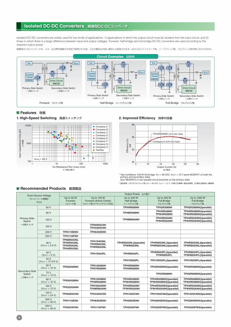
Single N-ch (VDSS = 30 V to 80 V) シングルNチャネルVDSS (V)
30 V 40 V 45 V 60 V 75 V 80 V
TPC6008-H
TPC8067-H
TPCC8067-H
TPC8066-H
TPCC8066-H
TPH11003NL
TPN11003NL
TPC8065-H
TPCC8065-H
TPCC8068-H
TP89R103NL
TPCA8068-H
TPC8064-H
TPCA8065-H
TPC8063-H
TP86R203NL
TPC8055-H
TPC8056-H
TPC8057-H
TPC8058-H
TPC8059-H
TPC8062-H
TPCC8064-H
TPCA8064-H
TPH8R903NL
TPN8R903NL
TPCA8063-H
TPCC8062-H
TPN6R003NL
TPCA8062-H
TPCA8059-H
TPCA8091-H*
TPCA8058-H
TPH6R003NL
TK40P03M1
TPH4R003NL
TPN4R303NL
TPCA8057-H
TK45P03M1
TPN2R703NL
TPH3R203NL
TPCA8056-H
TK50P03M1
TPCA8055-H
TPH1R403NL
TPHR9003NL
TPWR8503NL*
60
2525
16151111
11.411.611.6
9.111.68.4
11.4
7
6.22.12.42.83.24
5.88.28.28.98.96.8
5.66
5.6
3.8
6
36
10.84
4.32.69.72.7
3.22.2
7.5
1.9
1.40.9
0.85
TPC6009-H
TPC8089-H
TPC8052-H
TK15S04N1L*
TPC8047-H
TPC8045-H
TPC8046-H
TK20P04M1
TPCA8052-H
TPCA8047-H
TPCA8046-H
TK40P04M1
TPCA8045-H
TK50A04K3
TK50P04M1
TK65S04N1L*
TK80A04K3L
TK100S04N1L*
TPH1R204PL*
TPHR8504PL*
TPWR8004PL*
TK200F04N1L*
81
32
11.5
17.8
7.6
3.95.7
2911.3
7.3
5.4
11
3.6
3.58.7
4.3
2.4
2.3
1.240.850.80.9
TPH1R005PL* 1.04
TPCP8007-H
TPC6010-H
TPC8053-H
TPN22006NH
TPC8050-H
TPC8049-H
TPN14006NH
TPH14006NH*
TPCA8053-H
TPC8048-H
TPH11006NL
TPN11006NL
TPH7R506NH*
TK25S06N1S**
TPN7R506NH
TPCA8049-H
TPH5R906NH*
TK30A06N1
TK30E06N1
TPH4R606NH*
TPCA8048-H
TK40A06N1
TK40E06N1
TK58A06N1
TK58E06N1
TPH2R306NH*
TK90S06N1S**
TK100A06N1
TK100E06N1
57
59
22.522
14.5
10.714
14
22.3
6.9
11.411.4
7.5
18.57.5
10.45.915154.6
6.6
10.410.4
5.45.4
2.3
3.32.72.3
TK80A08K3
TPH2R608NH
TPW2R508NH*
4.5
2.62.5
TPN30008NH
TPC8051-H
TPN13008NH*
TPH12008NH
TPCA8051-H
TPH8R008NH*
TK35A08N1
TK35E08N1
TK46A08N1
TK46E08N1
TPH4R008NH
TK72A08N1
TK72E08N1
TK100A08N1
TK100E08N1
TPW4R008NH*
30
9.7
13.3
12.3
9.4
812.212.2
8.48.4
4
4.54.3
3.23.24
ID(A)
55.35.96.17.2
9
9.6
11
12
13
14
15
16
17
18
19
20
22242526
27
28
30
3234
35
38
40
42
45
46
4748
50
56
58
60
65
72
8090
100
116
150
200
RDS(ON) (m )
RDS(ON) (m )
RDS(ON) (m )
RDS(ON) (m )
RDS(ON) (m )
RDS(ON) (m )
High-speed switching高速スイッチング用
Load switchesロードスイッチ用Product Selection Guide 製品セレクションガイド
High-Speed Switching Series Designed for General-Purpose Switching Power Supply Applications高速スイッチングシリーズ 汎用スイッチング電源用
*: New Product **: Under Development*: 新製品 **: 開発中
10

Single N-ch (VDSS = 100 V to 250 V) シングルNチャネルVDSS (V)
100 V 120 V 150 V 200 V 250 V
TK8A10K3
TPN3300ANH
TK12A10K3
TPN1600ANH
TK18E10K3
TK22A10N1
TK22E10N1
TPH1400ANH*
TK25A10K3
TPH8R80ANH*
TK33S10N1H**
TK34A10N1
TK34E10N1
TK40A10N1
TK40E10N1
TK55S10N1*
TPH4R50ANH*
TK65A10N1
TK65E10N1
TK65G10N1
TPW4R50ANH*
TK100A10N1
TK100E10N1
TK160F10N1*
120
33
80
1642
13.813.813.640
8.8
9.7
9.59.5
8.28.2
6.5
4.54.84.84.5
4.53.83.42.4
TK32A12N1
TK32E12N1
TK42A12N1
TK42E12N1
TK56A12N1
TK56E12N1
TK72A12N1
TK72E12N1
13.813.8
9.49.4
7.57
4.54.4
TPH5900CNH
TPN5900CNH
TPH3300CNH
TPH1500CNH
TPW1500CNH*
5959
33
15.415.4
TPH1110ENH
TPN1110ENH
TPH6400ENH
TPH2900ENH
TPW2900ENH*
114114
64
2929
TPH2010FNH
TPN2010FNH
TPH1110FNH
TPH5200FNH
TPW5200FNH*
198198
112
5252
ID(A)
5.6
7.2
8
9
9.41012131718
22
2425
26
32
33
34
38
40
42
55
56
60
65
72
92
100
160
RDS(ON) (m )
RDS(ON) (m )
RDS(ON) (m )
RDS(ON) (m )
RDS(ON) (m )
Dual N-ch x 2 デュアルNチャネル × 2VDSS (V)
30 V 40 V 60 V 80 V
TPCP8205-H
TPC8224-H
TPC8223-H
262617
TPC8227-H 33TPC8228-H 57
80TPC8229-H
ID(A)
3.23.85.16.589
RDS(ON) (m )
RDS(ON) (m )
RDS(ON) (m )
RDS(ON) (m )
Built-in Schottky Barrier Diode SBD混載品VDSS (V)
30 V
TPCA8A11-H
TPCA8A10-H
TPCA8A09-H
3.63
2.3
ID(A)
354051
RDS(ON) (m )
TPC8 001-H
SOP-8 (new type)VS-6SOP-8 (conventional type)SOP Advance (conventional type)TSON Advance (conventional type)PS-8SOP Advance (new type)TSON Advance (new type)DSOP Advance
TP8
TPC6
TPC8
TPCA8
TPCC8
TPCP8
TPH
TPN
TPW
TP8
TPC6
TPC8
TPCA8
TPCC8
TPCP8
TPH
TPN
TPW
TO-220SISTO-220D2PAKTO-220SM(W)DPAKDPAK+
A
E
G
F
P
S
TK11 S 10N1L
Package パッケージ
For detailed information about individual MOSFETs, visit our website or see the SEMICONDUCTOR GENERAL CATALOG.
個別の製品の詳細につきましては、ウェブサイトまたは東芝半導体製品総覧表にてご確認ください。
*: New Product*: 新製品
**: Under Development**: 開発中
11

2.7 m max
2.2 m max
General-PurposeMOSFET汎用MOSFET
TPN2R703NL
Low On-ResistanceMOSFET
低オン抵抗MOSFET
TPN2R203NC
20% lower20%低減
SOP Advance
SOP Advance
SOP Advance withConnector technology
DSOP Advance
DSOP Advance
U-MOSVIIU-MOSIV
U-MOSVIII-H U-MOSVIII-H
U-MOSIX-H
MOSFETs with a VDSS of 30 VVDSS = 30 V耐圧品
Packaging Trendパッケージトレンド
2008
2.5
2
1.5
1
0.5
02010 2013 2014 2015
D2PAK
TO-220SM(W)
DSOP Advance
DSOP Advance
SOP Advance
SOP Advance
TSON Advance
PS-8
UDFN6
DPAK+
40 V to 250 V
20 V to 40 V
20 V to 30 V
TO-220
Available Packagesパッケージラインアップ
MOSFET Current RatingMOSFET電流定格
Package with Copper Connector& U-MOSVIII-H Processコネクタ構造パッケージ& U-MOSVIII-H プロセス
Source
Double-sided cooling両面から放熱
DSOP Advance
Top表面
Bottom裏面
As smartphones, tablet PCs and other mobile devices become more sophisticated and feature-rich, their battery drive circuits are
becoming more versatile and densely packed. Consequently, MOSFETs with small form factors, low on-resistance, high current
ratings, low capacitance and high permissible power dissipation are required. To meet these needs, Toshiba has developed new
process and packaging technologies to realize MOSFETs ideal for high-performance power supply applications.
スマートフォンやタブレットPCなどに代表される携帯機器のバッテリ駆動回路では、機器が多機能・高機能になるにしたがって、高性能化・高密度化が進んでいます。そのため、MOSFETには、小型・低オン抵抗・大電流・高許容損失といった特性が求められます。これらのニーズにお応えするため、プロセス技術とパッケージ技術の新規開発を進め、高性能な電源回路に貢献できるMOSFETを提案します。
Toshiba offers MOSFETs specifically optimized for
on-resistance, which exhibit lower on-resistance than those for
general-purpose switching power supply applications in the
same generation.
低オン抵抗に特化することで、同一世代の汎用スイッチング電源対応シリーズと比較して、より低いオン抵抗を実現しています。
Toshiba has endeavored to reduce the MOSFET on-resistance
by using the latest small-geometry process and improving
package structures.
最先端の微細加工技術の導入とパッケージ構造の改善にて、オン抵抗の継続的低減を実現しています。
Features 特長
Package パッケージ
The new device has a heat sink on both sides of the package to improve heat dissipation, making it possible to realize
high-current operations in compact packages.
パッケージ両面にチップから熱を逃がすための金属板を配置することにより、効率的な放熱を可能にし、小型パッケージでの大電流化要求に応えます。
Double-sided cooling Package DSOP Advance 両面放熱パッケージ
Dra
in-S
ourc
e O
n-R
esis
tanc
e R
DS
(ON
) (m
)ドレイン・ソース間オン抵抗
Dra
in-S
ourc
e O
n-R
esis
tanc
e R
DS
(ON
) ty
p. (
m)
ドレイン・ソース間オン抵抗
Dra
in-S
ourc
e V
olta
ge V
DS
S (
V)
ドレイン・ソース間電圧
1. Heat is removed from both the top and bottom surfaces.
The top metal plate is connected to the source. The source cannot
serve as an electrode to conduct electric current. Use it for heat
removal purposes.
2. Same footprint dimensions as for existing SOP Advance
SOP Advance can be replaced by the new package without modifying
an existing PCB layout.
1. 裏面/上面の両面から放熱します。上面金属板はソースに接続していますが、ソースを電極として通電させることはできませんので、放熱用としてご使用下さい。2. SOP Advanceパッケージ製品と裏面寸法(パッド寸法)が互換になっています。既存のプリント基板のレイアウトでそのまま置き換えることが可能です。
12
Low On-Resistance Series低オン抵抗シリーズ
Low Voltage MOSFET 低耐圧MOSFET

Product Selection Guide 製品セレクションガイド
Single Type (N-channel) シングルタイプ(Nチャネル)
Single Type (P-channel) シングルタイプ(Pチャネル)
SSM6K504NU
SSM6K513NU*
TPCF8003
TPCF8004
TPC6012
TPC6067
TPCP8009SSM6K514NU*
SSM6K341NU**
SSM6K361NU**
TPCP8011
TPCP8010
TPCP8013
TPCP8012
TPCA8082
TPCA8081
TPCA8080
TPCA8088
TPCA8087
TPCA8075
TPCA8078
TPCA8085
TPCA8086
TPCC8093
TPCC8074
TPN6R303NC
TPN2R503NC
TPN2R203NC
TPCC8084
TPCC8076
TPCC8073
TPN4R203NC
TPCC8069
TPCC8070
TPC8092
TPC8074
TPC8086
TPC8073
TPC8085
TPC8082
TPC8081
TPC8080
TPC8088
TPC8087
TPC8084
TPC8076
TPC8075
TPC8078
TK20S04K3L
TK35S04K3L
TK50S04K3L
TK8S06K3L
TK20S06K3L
TK30S06K3L
TK45S06K3L
TK80S06K3L
TK100F04K3
TK100F04K3L
TK100F06K3
TK130F06K3
TK80F08K3
TK70J06K3
TK75J04K3Z
TK70J04K3Z
20
30
33
40
60
75
TO-3P(N)TO-
220SM(W)DPAK+SOP-8SOP
AdvanceTSON
AdvancePS-8VS-6VS-8UDFN6BVDSS
(V)
20 to 18
6 to 524 to 23
20 to 8
8 to 6
6 to 4
4 to 2
2 to 0.87 to 66 to 4
4 to 2
32 to 23
15 to 10
10 to 4
4 to 2
60 to 4040 to 2020 to 1515 to 106 to 44 to 26 to 4
100 69
RDS(ON) max(m )
SSM6J512NU
SSM6J505NU
SSM6J511NU
SSN6J503NU
SSM6J502NU
SSM6J501NU
SSM6J507NU
TPCF8105
TPCF8108
TPCF8107
TPC6130
TPC6113
TPC6110
TPC6111
TPCP8105
TPCP8106
TPCP8109
TPCP8107
TPCP8111
TPCP8110
TPCC8136
TPCC8137
TPCC8138
TPN4R712MD
TPCC8131
TPCC8103
TPCC8105
TPCC8106
TPCC8107
TPH1R712MD
TPCA8131
TPCA8109TPCC8104
TPCA8128
TPCA8124
TPCA8122
TPCA8125
TPCA8123
TPCA8120
TPCA8121
TPC8129
TJ10S04M3L
TJ20S04M3L
TJ40S04M3L
TJ60S04M3L
TJ80S04M3L
TJ8S06M3L
TJ15S06M3L
TJ30S06M3L
TJ50S06M3L
TJ60S06M3L
TJ100F04M3L
TJ200F04M3L
TJ100F06M3L
TJ150F06M3L
TJ15P04M3
TPC8134
TPC8132
TPC8133
TPC8124
TPC8125
TPC8126
TPC8123
TPC8127
TPC8128
TJ9A10M3
TJ11A10M3
TJ20A10M3
–12
–20
–30
–40
–60
–100
TO-220SISTO-
220SM(W)DPAK+ DPAKSOP-8SOP
AdvanceTSON
AdvancePS-8VS-6VS-8UDFN6BVDSS
(V)
20 to10
110 to 10060 to 40
40 to 20
20 to 1510 to 88 to 66 to 4
2 to 0.8
40 to 2060 to 40
20 to 1515 to 10
8 to 66 to 4
10 to 8
4 to 2
60 to 40
15 to 1010 to 88 to 66 to 4
4 to 2
120 to 10060 to 4040 to 20
8 to 66 to 4
200 to 100
100 to 60
15 to 10
RDS(ON) max(m )
TPC8120
40 to 2020 to 15
For detailed information about individual MOSFETs, visit our website or see the SEMICONDUCTOR GENERAL CATALOG.
個別の製品の詳細につきましては、ウェブサイトまたは東芝半導体製品総覧表にてご確認ください。
*: New Product **: Under Development*: 新製品 **: 開発中
**: Under Development**: 開発中
SSM6J509NU**SSM6J508NU**
13

3 pin
2.9 x 2.8 mm
S-MINI
CST3B
USM SSM VESM CST3 CST3C
SOT-23F
2.0 x 2.1 mm
8 pin
PS8 VS8
2.9 x 1.5 mm
1.6 x 1.6 mm
1.5 x 1.5 mm
1.2 x 1.2 mm
WCSP6C
1.0 x 1.5 mm
1.2 x 0.8 mm
1.0 x 0.6 mm 0.8 x 0.6 mm
High PD
High PD
New
New
New
UnderDevelopment
UFMTSM
5 pin
SMV USV ESV
6 pin
VS6 US6
UF6
ES6
WCSP9
UDFN6
High PD
TSOP6F
UFV
30-V MOSFETs30 V耐圧品60-V MOSFETs60 V耐圧品
20-V MOSFETs20 V耐圧品60-V MOSFETs60 V耐圧品
RonA Reduction of N-Channel MOSFETs
N-ch MOSFETのRonA低減トレンド
Roughly 60% to 70% reduction
約60~70%ダウン
Roughly 60% to 70% reduction
約60~70%ダウン Roughly 70% reduction約70%ダウン
Roughly 70% reduction約70%ダウン
RonA Reduction of P-Channel MOSFETs
P-ch MOSFETのRonA低減トレンド
1.0
1.2
0.8
0.6
0.4
0.2
0.0U-MOSVIII-HU-MOSVII U-MOSIX-H U-MOSVII U-MOSVIIIU-MOSVIU-MOSV
1.0
1.2
0.8
0.6
0.4
0.2
0.0
Relative RonA Reduction
RonA低減率(%)
Relative RonA Reduction
RonA低減率(%)
UnderDevelopment
Housed in a tiny package with a small footprint, MOSFETs of this series can be placed anywhere on a printed circuit board and thus
help reduce the size of end-products. These MOSFETs are suitable for use as general-purpose switches in various drive circuits and
communication lines.
小型パッケージに搭載することで、実装面積を削減し、機器の小型化に貢献します。各種の駆動回路や通信ラインの汎用スイッチとして、実装箇所を気にすることなく使用できます。
Features 特長
Extensive packaging options are available, ranging from a package measuring 3.0 mm x 3.0 mm to an ultra-small package measuring
less than 1.0 mm x 1.0 mm. These packages feature a small form factor, low on-resistance and high permissible power dissipation.
3.0 × 3.0 mmから 1.0 × 1.0 mmクラス以下の超小型パッケージまで幅広いラインアップ製品を提供します。小型、低オン抵抗、高許容損失の特長があります。
Package パッケージ
Fabricated using the latest trench process, MOSFETs of this series provide the industry's lowest-class on-resistance. Furthermore,
process tuning is performed to achieve low-voltage operation. An integrated protection diode provides an improved trade-off between
the chip size and ESD immunity.
最新のトレンチプロセスを使用し、業界最高水準の低オン抵抗特性をもった製品を提供します。また、プロセスチューニングを行い、低電圧駆動化を実現しています。チップ小型化に伴うESD耐量低下に関しては、保護ダイオード内蔵により、そのトレードオフを改善しました。
14
Small Package Series小型パッケージシリーズ
Low Voltage MOSFET 低耐圧MOSFET
SSM3K56ACT*
SSM3K59CTB*
SSM3K56MFV*
SSM6K781G*
SSM3K56FS
12
20
40
±8±8±8±12
70.81.42
18235235228
4.54.54.54.5
6005555130
Semi-Power Type セミパワータイプ
Single N-ch (1) シングルNチャネル (1)Package パッケージAbsolute Maximum Ratings
絶対最大定格RDS(ON)
(m )
Ciss(pF)
CST3SOT-883
CST3B VESMSOT-723
WCSP6C SSMSOT-416
@|VGS|(V)maxVDSS
(V)VGSS
(V)ID
(A)
SSM3J56ACT*
SSM3J46CTB
SSM3J56MFV
SSM6J771G*
–20
±8±8±8±12
–0.8–1.4–2–5
39039010335
4.54.54.54.5
100100290870
Single P-ch (1) シングルPチャネル (1)Package パッケージAbsolute Maximum Ratings
絶対最大定格RDS(ON)
(m )
Ciss(pF)
CST3SOT-883
CST3B VESM WCSP6C
@|VGS|(V)maxVDSS
(V)VGSS
(V)ID
(A)
SSM6K204FE
SSM6K211FE
SSM6K208FE
SSM6K217FE*
SSM6K504NU*
SSM6K513NU*
SSM6K514NU*
SSM6K341NU**
SSM6K361NU**
SSM3K122TU
SSM3K121TU
SSM3K123TU
SSM3K127TU
SSM3K116TU
SSM3K131TU
SSM3K2615TU*
SSM6K404TU
SSM6K403TU
SSM6K411TU
SSM6K406TU
SSM6K407TU
SSM3K336R
SSM3K329R
SSM3K324R*
SSM3K333R
SSM3K335R
SSM3K337R
SSM3K339R*
SSM3K2615R*
SSM3K318R*
SSM3K341R*
SSM3K361R*
SSM6K803R**
SSM6K804R**
20
30
38
40
60
100
±10±10±10±10±10±10±10±12±12±12±12±20±12±12±20±20±20±20±20±20±20±12±12±20±20±20±20±20±20±20±20
2
3
3.2
4.2
101.92
2.23
3.54
4.4
6
9152
1.8212
2
2.56
3.5
12612355474828281213312310014012656
38.541.54256261217620819817.3440440440145519292
444
4.5444
4.544
4.54.54
4.54.54.54.54.54.54.54.54.54.54.5444
4.54.54.54.5
1951954005104001010105071012312324512612320049045043634062011301201301301110150150150235550430430
Single N-ch (2) シングルNチャネル (2)Package パッケージAbsolute Maximum Ratings
絶対最大定格RDS(ON)
(m )
Ciss(pF)
ES6SOT-563
UDFN6B UFM UF6 SOT-23F TSOP6F
@|VGS|(V)maxVDSS
(V)VGSS
(V)ID
(A)
For detailed information about individual MOSFETs, visit our website or see the SEMICONDUCTOR GENERAL CATALOG.
個別の製品の詳細につきましては、ウェブサイトまたは東芝半導体製品総覧表にてご確認ください。
High-speed switching高速スイッチング用
Load switchesロードスイッチ用Product Selection Guide 製品セレクションガイド
*: New Product*: 新製品
*: New Product **: Under Development*: 新製品 **: 開発中
*: New Product*: 新製品
15

SSM6J216FE
SSM6J213FE
SSM6J215FE
SSM6J212FE
SSM6J207FE
SSM6J214FE
SSM6J512NU*SSM6J505NUSSM6J511NU*
SSM6J502NUSSM6J503NU
SSM6J501NU
SSN6J509NU**
SSM6J508NU**SSM6J507NU*
SSM3J132TU
SSM3J135TUSSM3J134TU
SSM3J130TUSSM3J133TU
SSM3J112TUSSM3J118TU
SSM3J117TU
SSM6J50TU
SSM6J412TU*
SSM6J414TU
SSM6J402TUSSM6J410TUSSM6J401TU
SSM3J338R*
SSM3J327RSSM3J331R
SSM3J328R
SSM3J334RSSM3J340R*
SSM3J332R
SSM3J356R*SSM3J351R**
SSM8J801R**
±8±6±10±10±6±10±8±12±10±8±8±8±8±8±8±8±8±8±8±8±8±8±8±8±20±20±20±20
–25/+20±20±20±20±12±20
–25/+20–25/+20
±12–25/+20–25/+20–20/+10–20/+10
3217
20.218.712101501366410310393599355
40.742.725.829.829.823.132.422.515.3790480491225270225393145571056666504028360200
4.54.54.54.54.54.54.54.54.54.54.54.54.54.54.54.54.54.54.54.54.54.54.54.54444
4.5444
4.54.54.54.54.54.54.54.54.5
10402700140014002700335027021080029027029063029063097084018008408401800840165026008613713728017528012073056028060060056010831150330491
Single P-ch (2) シングルPチャネル (2)Package パッケージAbsolute Maximum Ratings
絶対最大定格RDS(ON)
(m )
Ciss(pF)
ES6SOT-563
UDFN6B UFM UF6 SOT-23F
SSM3J325FSSM3J352F*
SSM3J353F**
S-MiniSOT-346
TSOP6F
@|VGS|(V)maxVDSS
(V)VGSS
(V)ID
(A)
–4.8–5.4–6–10–12–14
–2
–2.5–2.6–3
–3.2–3.4–3.9
–4
–4.4–5.5
–6
–10–1.1
–1.4
–2
–2.1–2.5–3.6
–4
–6
–10–2
–2.5
–12
–20
–30
–60
SSM6N56FE*
SSM6P41FE
SSM6L14FE
SSM6N61NU*
SSM6N55NUSSM6N57NUSSM6N58NU
SSM6P47NUSSM6P49NU
SSM6L61NU*
SSM6H19NU*
SSM6G18NU
SSM6N62TU**SSM6N39TU
SSM6N24TUSSM6N40TU
SSM6P54TUSSM6P39TU
SSM6P40TU
SSM6L39TU
SSM6L12TU
SSM6L40TU
SSM3H137TU*
SSM5H08TUSSM5H90ATUSSM5H01TUSSM5H11TUSSM5H16TU
SSM5G02TUSSM5G09TU
SSM5G11TU
±8±8±10±8±12±20±20±12±12±8±8±8±8±12±20±10±8±10±8±8±12±12±12±20±20±12±10±20±20±12±12±12±8±8±20±20
235951193314518264
39.1843002282139556403240300119213335614526018240316065450182133198160130112403280
4.54.54
4.54.54
4.54.54.54.52.54
4.54.54
4.54.544
4.54.54.544444444
4.544
4.54
4.5
5521526041024518028031012911033125029048012090110260250410480245218180120125200106180123130310550270120119
Dual channel/Complementary デュアルチャネル/コンプリメンタリPackage パッケージAbsolute Maximum Ratings
絶対最大定格Polarity極性
RDS(ON) (m )
Ciss(pF)
ES6SOT-563
UDFN6B UF6 UFM UFV
@|VGS|(V)maxVDSS
(V)VGSS
(V)ID
(A)
0.8
1.64
0.51.6
4
–0.72–1.2–1.5
–4
–1.40.8
–0.721.6–1.5
4–40.5–0.51.6–1.41.52.41.41.61.92–1
–1.5–2
–1.42
20
30
–20
–3020–2020–2020–2030–2030–30
20
30
40
–12
–20–3034
N-ch x 2
P-ch x 2
N-ch + P-ch
N-ch + SBD
P-ch + SBD
N-ch + ZD
*: New Product **: Under Development*: 新製品 **: 開発中
*: New Product **: Under Development*: 新製品 **: 開発中
16

Small-Signal Standard Type 小信号スタンダードタイプ
SSM3K35CTC*
SSM3K15ACTC*
SSM3K72CTC*
SSM3J35CTC*
SSM3K35CT
SSM3K37CT
SSM3K56ACT*
SSM3K15ACT
SSM3K72KCT*
SSM3J35CT
SSM3J56ACT*
SSM3J15CT
SSM3K35MFV
SSM3K37MFV
SSM3K36MFV
SSM3K56MFV*
SSM3K15AMFV
SSM3K44MFV
SSM3J35MFV
SSM3J36MFV
SSM3J56MFV
SSM3J15FV
SSM3K35FS
SSM3K37FS
SSM3K36FS
SSM3K56FS
SSM3K15AFS
SSM3K44FS
SSM3K72CFS*
SSM3K72KFS*
SSM3J35FS
SSM3J36FS
SSM3J15FS
SSM3K36TU
SSM3J36TU
±10±10±10±10±10±8±8±20±20±20±7±20±20±20±20±20±10±10±8±8±8±20±20±20
32.21.12.20.660.2350.2353.64
1.2204.74.74.71.751.75
81.51.310.390.39124.22
44.54.54.54.54.54.54444
4.54.54.54.54.54
4.54.54.54.54410
Single N-ch/P-ch シングル Nチャネル/PチャネルPackage パッケージAbsolute Maximum
Ratings絶対最大定格Polarity
極性
RDS(ON)
( ) CST3C CST3SOT-883
VESMSOT-723
SSMSOT-416
UFM USMSOT-323
SOT23 S-Mini
@|VGS|(V)maxVDSS
(V)VGSS
(V)ID
(A)
0.180.2
0.25
0.50.81.4
0.1
0.40.10.150.170.20.40.4–0.1–0.25–0.33–0.8–1.4–0.1–0.2–0.2
20
30
50
60
–20
–30
–60
N-ch
P-ch
T2N7002AK*
T2N7002BK*
SSM3K15F
SSM3K7002KF*
SSM3J15F
SSM3J168F**
SSM5N16FE
SSM5N15FE
SSM5P16FE
SSM5P15FE
SSM6N35FE
SSM6N37FE
SSM6N36FE
SSM6N56FE
SSM6N44FE
SSM6P16FE
SSM6P35FE
SSM6P36FE
SSM6P15FE
SSM6L35FE
SSM6L36FE
SSM5N16FU
SSM5N15FU
SSM5P16FU
SSM5P15FU
SSM6N36TU
SSM6P36TU
SSM6L36TU
SSM6N35FU
SSM6N37FU
SSM6N43FU
SSM6N15AFU
SSM6N44FU
SSM6N09FU
SSM6N17FU
SSM6N7002CFU*
SSM6N7002KFU*
SSM6P16FU
SSM6P35FU
SSM6P15FU
SSM6P09FU
SSM6L35FU
SSM6L09FU
SSM3K16FU x 2
SSM3K35FS x 2
SSM3K37MFV x 2
SSM3K36FS x 2
SSM3K56FS x 2
SSM6N56FE x 2
SSM3K15FU x 2
SSM3K44FS x 2
SSM3K09FU x 2
SSM3K17FU x 2
T2N7002AK x 2
T2N7002BK x 2
SSM3J16FU x 2
SSM3J35FS x 2
SSM3J36FS x 2
SSM3J15FU x 2
SSM3J09FU x 2
SSM3K35FS
+SSM3J35FS
SSM3K36FS
+SSM3J36FS
SSM3K09FU
+SSM3J09FU
±10±10±10±10±8±20±20±20±20±7±20±20±10±10±8±20±20±10±10±10±8±20±20
44
4.54.54.544444
4.54.544
4.54444
4.54.544
Dual N-chx2/P-chx2/N-ch+P-ch デュアル Nチャネル×2/Pチャネル×2/Nチャネル+PチャネルPackage パッケージAbsolute Maximum
Ratings絶対最大定格Polarity
極性
Constituent Devices構成デバイス
RDS(ON) ( ) ESV
SOT-553ES6
SOT-563USV
SOT-353UF6 US6
SOT-363
@|VGS|(V)
33
2.20.660.2353.644
1.2204.71.75
88
1.31124.238
0.661.311.24.2
maxVDSS
(V)VGSS
(V)ID
(A)
0.10.180.250.50.8
0.1
0.40.10.170.3
–0.1
–0.33–0.1–0.20.18–0.10.5
–0.330.4–0.2
20
30
50
60
–20
–30
20–2020–2030–30
N-ch x 2
P-ch x 2
N-ch + P-ch
SSM3K15AFU
SSM3K09FU
SSM3K17FU
SSM3K7002CFU*
SSM3K7002KFU*
SSM3J15FU
SSM3J09FU
High-speed switching高速スイッチング用
Load switchesロードスイッチ用Product Selection Guide 製品セレクションガイド
*: New Product **: Under Development*: 新製品 **: 開発中
*: New Product*: 新製品
For detailed information about individual MOSFETs, visit our website or see the SEMICONDUCTOR GENERAL CATALOG.
個別の製品の詳細につきましては、ウェブサイトまたは東芝半導体製品総覧表にてご確認ください。
17

DTMOSIV Standard Series VDSS =スタンダードシリーズ 500 V 600 V 650 V 800 V
DTMOSIV (HSD) High-Speed Diode Series 高速ダイオードシリーズ 600 V 650 V
DTMOSIV-H High-Speed Switching Series 高速スイッチングシリーズ 600 V
280 ns
100 ns
t: 80 ns/div ID = 10 A/div
TK16A60W5High-Speed Diode
高速ダイオード品
Qg
Qgd
170 nC
72 nC
Qg
Qgd
144 nC
48 nC
t: 20 s/divQg: 20 nC/div
VGS: 2 V/div
Qg: Approx.20% fasterQgd: Approx.30% faster
Qg: 約20%高速化Qgd: 約30%高速化ID: 20 A/div
VDS: 100 V/div
t: 20 s/divQg: 20 nC/div
VGS: 2 V/div
ID: 20 A/div
VDS: 100 V/div
TK62N60WStandard
スタンダード品
TK62N60XHigh-Speed Switching
高速スイッチング品
TK16A60WStandard
スタンダード品
VDSS =
VDSS =
Power MOSFETs are indispensable for converters, inverters and other switching power supplies. DTMOS is a power MOSFET series with a
superjunction structure that feature high current-switching capability. With a VDSS of 600 V or so, DTMOS is suitable for mid- to high-voltage
applications.
コンバータやインバータなどのスイッチング電源に欠かせないパワーMOSFETです。スーパージャンクション構造により大電流化を図っています。耐圧 600 Vを中心としたラインアップで、中高耐圧アプリケーションに適しています。
Fabricated using a state-of-the-art single-epitaxial process, the DTMOSIV series exhibits an RonA lower than 15 m ·cm2. The reduction in
RonA, a performance index for MOSFETs, directly translates to a reduction in conduction loss, which helps improve the efficiency and
reduce the size of power supplies.
最新のシングルエピタキシャルプロセスの採用により、性能指標 RonAが 15 m ・cm2を下回る性能を実現しています。RonAの性能向上により導通損失を抑え、電源機器の効率改善を実現すると共に、小型化に大きく貢献します。
Toshiba is planning to expand its MOSFET portfolio to meet diverse customer needs.
ご要望に合わせて、さまざまなラインアップ展開を計画中です。
Product Lineup 製品のラインアップ展開
DTMOSIV-H High-Speed Switching Series 高速スイッチングシリーズ
DTMOSIV (HSD) High-Speed Diode Series 高速ダイオードシリーズ
The DTMOSIV (HSD) Series has a parasitic diode faster than that of the standard series. It delivers
reverse recovery time more than 70% shorter than the standard series, and thus significantly reduces
the recovery loss incurred by the parasitic diode.
MOSFET内蔵寄生ダイオードの高速化を実現したシリーズです。スタンダード品に比べて逆回復時間が70%以上短いため、寄生ダイオードで発生するリカバリ損失を大幅に低減させることができます。
The DTMOSIV-H Series features high-speed switching performance and thus low switching loss. It provides gate-drain capacitance, Qgd, approximately 30%
lower than standard MOSFET series.
高速スイッチング特性により、低スイッチング損失を実現したシリーズです。スタンダード品に比べて、Qgd(ゲート・ドレイン間容量)を約30%削減しています。
Fourth-Generation Super-Junction DTMOS Series (DTMOSIV)第4世代 スーパージャンクション DTMOSシリーズ (DTMOSIV)
DTMOSIV
Part Number 品番
Rating 定格
On-Resistance オン抵抗
Reverse Recovery Time: trr リカバリ時間
Standard スタンダード品
TK16A60W
600 V/15.8 A
0.19 Max
280 ns
High-Speed Diode 高速ダイオード品
TK16A60W5
600 V/15.8 A
0.23 Max
100 nsReverse-Recovery Waveform of the Parasitic Diode
寄生ダイオードリカバリ時波形
Dynamic Input/Output Characteristics: Qg Curvesダイナミック入出力特性: Qg 波形
Comparisons of Typical Performance Characteristics代表製品特性比較表 * Test condition: VDD = 400 V, IDR = 7.9 A, TC = 25 ˚C
* 測定条件: VDD = 400 V、IDR = 7.9 A、TC = 25℃
18
DTMOS SeriesDTMOSシリーズ
Mid-High Voltage MOSFET 中高耐圧MOSFET

Product Selection Guide 製品セレクションガイド
DTMOSIV Standard Series スタンダードシリーズ
DTMOSIV-H High-Speed Switching Series 高速スイッチングシリーズ
DTMOSIV (HSD) High-Speed Diode Series 高速ダイオードシリーズ
Package パッケージ
TK16V60W5
TK20V60W5
TK25V60X5
TK31V60W5
TK22V65X5**
TK28V65X5**
TK5P60W5**
TK7P60W5
TK8P60W5*
TK16G60W5
TK14G65W5
TK5A60W5*
TK7A60W5
TK8A60W5
TK10A60W5
TK16A60W5
TK20A60W5
TK25A60X5
TK14A65W5
TK17A65W5
TK22A65X5**
TK35A65W5
TK14C65W5
TK16E60W5
TK20E60W5
TK25E60X5
TK14E65W5
TK16J60W5
TK20J60W5
TK31J60W5
TK39J60W5
TK62J60W5
TK16N60W5
TK20N60W5
TK25N60X5
TK31N60W5
TK39N60W5
TK62N60W5
TK14N65W5
TK28N65W5
TK35N65W5
TK49N65W5
0.99 to 0.950.67 to 0.650.56 to 0.54
0.450.245 to 0.230.19 to 0.1750.15 to 0.14
0.109 to 0.0990.0740.045
0.30.23
0.17 to 0.160.14 to 0.13
0.0950.057
TO-247TO-3P(N)TO-220SIS TO-220DFN8x8 D2PAK I2PAKDPAKRDS(ON) max( )
VDSS
(V)
600
650
For detailed information about individual MOSFETs, visit our website or see the SEMICONDUCTOR GENERAL CATALOG.
個別の製品の詳細につきましては、ウェブサイトまたは東芝半導体製品総覧表にてご確認ください。
*: New Product*: 新製品
**: Under Development**: 開発中
Package パッケージ
TK10V60W
TK12V60W
TK16V60W
TK20V60W
TK31V60W
TK14V65W*
TK17V65W*
TK28V65W*
TK5P60W
TK6P60W
TK7P60W
TK8P60W
TK10P60W
TK12P60W
TK5P65W
TK6P65W
TK7P65W
TK8P65W
TK9P65W
TK11P65W
TK3P80W**
TK6P80W**
TK16G60W
TK20G60W
TK14G65W
TK5Q60W
TK6Q60W
TK7Q60W
TK8Q60W
TK10Q60W
TK12Q60W
TK5Q65W
TK6Q65W
TK7Q65W
TK8Q65W
TK9Q65W
TK11Q65W
TK3Q80W**
TK6Q80W**
TK10A50W
TK12A50W
TK19A50W
TK5A60W
TK6A60W
TK7A60W
TK8A60W
TK10A60W
TK12A60W
TK16A60W
TK20A60W
TK31A60W
TK39A60W
TK5A65W
TK6A65W
TK7A65W
TK8A65W
TK9A65W
TK11A65W
TK14A65W
TK17A65W
TK28A65W
TK35A65W
TK7A80W**
TK10A80W**
TK12A80W*
TK17A80W
TK16C60W
TK20C60W
TK14C65W
TK17C65W
TK10E60W
TK12E60W
TK16E60W
TK20E60W
TK31E60W
TK14E65W
TK17E65W
TK28E65W**
TK7E80W**
TK10E80W**
TK12E80W**
TK17E80W**
TK12J60W
TK16J60W
TK20J60W
TK31J60W
TK39J60W
TK62J60W
TK16N60W
TK20N60W
TK31N60W
TK39N60W
TK62N60W
TK14N65W
TK17N65W
TK28N65W
TK35N65W
TK49N65W
TK12N80W**
TK17N80W**
TK100L60W
0.380.300.190.9
0.82 to 0.750.60.5
0.43 to 0.380.34 to 0.30
0.190.17 to 0.155
0.098 to 0.0880.0650.040.018
1.22 to 1.201.05 to 1.00.8 to 0.780.67 to 0.650.56 to 0.500.44 to 0.390.28 to 0.250.21 to 0.200.12 to 0.11
0.080.0552.251.05 0.9
0.65 to 0.550.450.29
TO-3P(L)TO-247TO-3P(N)TO-220SIS TO-220DFN8x8 D2PAK I2PAKIPAKDPAKRDS(ON) max( )
VDSS
(V)
500
600
650
800
*: New Product*: 新製品
Package パッケージ
TK25V60X
TK31V60X
TK25A60X TK25E60X
TK31E60X
TK25N60X
TK31N60X
TK39N60X
TK62N60X
TK25Z60X*
TK31Z60X*
TK39Z60X*
TK62Z60X*
0.135 to 0.1250.098 to 0.088
0.0650.04
TO-247TO-220SIS TO-220DFN8x8RDS(ON) max( )
VDSS
(V)
600
TO-247-4L
*: New Product **: Under Development*: 新製品 **: 開発中
19

76%
78%
80%
82%
84%
86%
88%
90%
0 20 40 60 80 100 120 140
2SK3569TK10A60D
Pout (W)
Effi
cien
cy効率
Efficiency greater than a -MOSVI MOSFET-MOSVIとの同等以上の効率を実現
Rg = 47
Rg = 47
Rg = 4.7 Rg = 4.7
MAIN
SynchronousRectifier
VIN
VOUT
2SK3569
vs
TK10A60D
+–
+–
+–
120 W (20 V/6 A) Flyback ConverterVIN = 100 VAC, VGS = +10, −0 V
PFC
0
500
400
300
200
100
020 40 60 80 100
Turn
-Off
Tim
e to
ff (n
s)ターンオフ時間
Gate Resistance rg ( ) ゲート抵抗
Test conditions : VDS = 400 V VGS = 10 V ID = 4.5 A TC = 25℃
toff-rg 特性
TK9J90E
2SK3878
Faster switching speedLower switching lossスイッチングスピード高速化低スイッチング損失
Faster switching speedLower switching lossスイッチングスピード高速化低スイッチング損失
0 10 20 30 40 50 60 70 80 0 10 20 30 40 50 60 70 80
Qg (nC) Qg (nC)
VGS = 10 VVGS = 10 V
VDS: 50 V/div
VGS: 2.5 V/divID: 3 A/div
VGS: 2.5 V/divID: 3 A/div
VDS: 50 V/div
The -MOSVII Series, the latest addition to our -MOS portfolio, features reduced capacitance by virtue of the optimized chip design.
The -MOSVII Series has significantly expanded our MOS product lineup.
チップデザインの最適化により、容量特性を低減した -MOSの最新シリーズです。ラインアップを大幅に拡充しました。
Efficiency Test Circuit 効率評価
Performance Comparisons Between -MOSVII and -MOSVI Devices (600 V/10 A) 新世代 -MOSVIIシリーズと従来の -MOSVIシリーズとの特性比較(600 V/10 A定格品)
-MOSVII Series (VDSS = 400 V to 650 V) -MOSVII シリーズ
● Delivers approximately 40% lower total gate charge, Qg, than -MOSVI.● Available in 50 V steps of VDSS and in finer steps of RDS(ON).● Rated avalanche and reverse recovery current capabilities.
● -MOSVIに比べて、Qg(ゲート入力電荷量)を約40%低減。● 耐圧の50 Vステップ化、および、オン抵抗の細分化によるラインアップの拡充。● アバランシェ耐量、逆リカバリ耐量の定格電流保証。
-MOSVIII Series (VDSS = 800 V to 900 V) -MOSVIII シリーズ
Features 特長
● Exhibits approximately 25% lower total gate charge, Qg, than -MOSVII (rated at 800 V to 900 V).
● Guarantees avalanche and reverse recovery ruggedness as current ratings.● -MOSVII (800 V~900 V)に比べて、Qg(ゲート入力電荷量)を約25%低減。● アバランシェ耐量、リバースリカバリ耐量の定格電流保証。
Features 特長
Switching Waveforms スイッチング波形
Provides approx. 25% lower Qg than the previous generation and thus reduces
switching loss
前世代に比べて、Qgを約25% 低減、スイッチング時の損失低減。
Comparisons of Total Gate Charge (Qg)
Qg(ゲート入力電荷量)特性比較
-MOSVII
TK10A60D
600 V/10 A
TO-220SIS
-MOSVI
2SK3569
600 V/10 A
TO-220SIS
Symbol 記号
IGSS
IDSS
VDSF
Qg
RDS(ON)
V(BR)DSS
Vth
Characteristic 項目
Gate leakage current ゲート漏れ電流Drain cut-off current ドレイン遮断電流
Gate threshold voltage ゲートしきい値電圧
Total gate charge ゲート入力電荷量
Diode forward voltage 順電圧(ダイオード)
Drain-source breakdown voltage ドレイン・ソース間降伏電圧
Drain-source on-resistance ドレイン・ソース間 オン抵抗
Series シリーズ
Part Number 品番
Ratings 定格
Package パッケージ
Test Conditions 測定条件
VGS condition*, VDS = 0 V VDS = 600 V, VGS = 0 V
ID = 10 mA, VGS = 0 V
IDR =10 A, VGS = 0 V
VDS = 10 V, ID = 1 mA
VGS = 10 V, ID = 5 A
VDD = 400 V, VGS = 10 V, ID = 10 A
min typ. max
− − ±1
− 10
600 − −
2.0 −
−
4.0
− 25 −
− − –1.7
− 0.75
min typ. max
− − ±10
− − − 100
600 −
−
−
2.0
−
4.0
− 42 −
− − –1.7
− 0.75
Unit 単位
A
A
V
V
nC
V
* Test Conditions: VGS = ±30 V (TK10A60D), VGS = ±25 V (2SK3569)* 測定条件: VGS = ±30 V (TK10A60D)、VGS = ±25 V (2SK3569)
-MOSIV
2SK3878
60nC (@VGS = 10 V)
-MOSVIII
TK9J90E
46nC (@VGS = 10 V)Qg
VG
S-Q
g, V
DS-Q
g W
avef
orm
sV
GS-Q
g, V
DS-Q
g 波形
Gen.世代
Part Number品番
20
π-MOS Seriesπ-MOSシリーズ
Mid-High Voltage MOSFET 中高耐圧MOSFET

Package パッケージ
Product Selection Guide 製品セレクションガイド
For detailed information about individual MOSFETs, visit our website or see the SEMICONDUCTOR GENERAL CATALOG.
個別の製品の詳細につきましては、ウェブサイトまたは東芝半導体製品総覧表にてご確認ください。
TK20 A 20D
TO-220SISTO-220
TO-3P(N)TO-3P(N)IS
New PW-Mold/DPAKNew PW-Mold2
A
E
J
M
P
Q
TO-220SIS
TO-3P(N)
2SK3564
2SK3566
2SK3798
2SK3633
2SK4207
VDSS (V)
200 250 300 450 500 525
TK9A20DA
TK15A20D
TK20A20D
TK25A20D
TK40J20D
TK70J20D
0.4
0.18
0.1090.07
0.044
0.027
0.50.5
0.250.250.25
0.15
0.1
0.06
0.038
1.75
1.35
1.2
1.1
0.9
0.77
0.620.52
0.46
0.410.34
0.27
0.25
322
1.51.5
1.4
1.221.22
1.04
0.85
0.720.60.520.47
0.4
0.30.4
0.27
0.27
1.7
1.51.5
1.31.3
0.58
0.139
0.052
TK4A55DA
TK4P55DA
TK4A55D
TK4P55D
TK5A55D
TK6A55DA
TK7A55D
TK8A55DA
TK9A55DA
TK10A55D
TK11A55D
TK12A55D
TK12J55D
TK13A55DA
TK14A55D
TK16A55D
TK16J55D
TK19J55D
TK8A25DA
TK8P25DA
TK13A25D
TK13E25D
TK13P25D
TK17A25D
TK20A25D
TK30J25D
TK60J25D
TK18A30D
TK50J30D
TK5A45DA
TK6A45DA
TK7A45DA
TK8A45DA
TK8A45D
TK9A45D
TK11A45D
TK12A45D
TK13A45D
TK14A45DA
TK14A45D
TK16A45D
TK19A45D
TK3P50D
TK4A50D
TK4P50D
TK5A50D
TK5P50D
TK6A50D
TK7A50D
TK7P50D
TK8A50DA
TK8A50D
TK10A50D
TK11A50D
TK12A50D
TK13A50DA
TK13A50D
TK15A50D
TK15J50D
TK18A50D
TK20J50D
TK4A53D
TK5A53D
TK5P53D
TK6A53D
TK6P53D
TK12A53D
ID(A)
88.59101112
12.5
13
13.514
15
16
1817
1920253040506070
3
4
4.5
5
6
6.5
7
7.5
5.5
88.5
9
10
11
12
12.5131415
16
19
3
2.5
2
1
3.5
3.7
4
4.55
6
7
7.5
5.5
RDS(ON) ( ) RDS(ON) ( )RDS(ON) ( ) RDS(ON) ( )RDS(ON) ( ) RDS(ON) ( )RDS(ON) ( ) RDS(ON) ( )RDS(ON) ( ) RDS(ON) ( )
2.452.45
1.881.88
1.71.48
1.25
1.07
0.86
0.72
0.630.570.570.48
0.37
0.330.370.33
TK2P60D
TK2Q60D
TK3A60DA
TK4A60DA
TK4P60DA
TK4Q60DA
TK4A60DB
TK4P60DB
TK4A60D
TK4P60D
TK5A60D
TK6A60D
TK8A60DA
TK9A60D
TK10A60D
TK11A60D
TK12A60D
TK13A60D
TK15A60D
4.34.3
2.8
2.22.22.222
1.71.7
1.43
1.25
1
0.83
0.75
0.65
0.55
0.43
0.37
TK2A65D
TK3A65DA
TK3A65D
TK4A65DA
TK5A65DA
TK5A65D
TK6A65D
TK7A65D
TK8A65D
TK11A65D
TK12A65D
TK13A65D
3.26
2.51
2.25
1.9
1.671.43
1.11
0.98
0.84
0.7
0.54
0.47
TK3P80E
TK4A80E*
TK5A80E*
TK6A80E
2SK3633
TK10A80E
TK10J80E
4.9
3.5
2.4
1.7
1.7
11
TK1Q90A
TK2P90E
2SK3566
TK3A90E*
2SK3564
2SK3798
TK5A90E*
TK7A90E
TK7J90E
TK9A90E
TK9J90E
2SK4207
9
5.9
6.44.64.3
3.5
3.1
22
1.31.3
0.95
VDSS (V)
550 600 650 800 900ID(A) RDS(ON) ( ) RDS(ON) ( )RDS(ON) ( ) RDS(ON) ( )RDS(ON) ( ) RDS(ON) ( )RDS(ON) ( ) RDS(ON) ( )RDS(ON) ( )
*: New Product*: 新製品
21

0.0
0.2
0.4
0.6
0.8
1.0
1.2
U-MOSVIU-MOSIII0.0
Next generation次世代
Next generation次世代
0.2
0.4
0.6
0.8
1.0
1.2
U-MOSVIII U-MOSIXU-MOSIV
Nch MOSFET
Approx.60% Reduction約60%ダウン
Approx.60% Reduction約60%ダウン
Pch MOSFET
RonA Reduction Trend (VDSS = 40 V) RonAの低減トレンド(VDSS = 40 V 系)
Ron
A R
educ
tion
(Nor
mal
ized
to U
-MO
SIV
)RonA低減率 (U-MOSI
Vで規格化)
Ron
A R
educ
tion
(Nor
mal
ized
to U
-MO
SII
I)RonA低減率 (U-MOSI
IIで規格化)
Cur
rent
Rat
ing
(A)
電流定格
Mounting Area (mm2) 実装面積
Frameフレーム
Cu ClampCuクランプ
Chipチップ
Note: Comparisons of MOSFETs with 40 V VDSS
注: 40 V耐圧比較
TSON Advance
PS-8SOP-8
New PW-Mold
DPAK+
TO-220SM(W)
TO-220SM(Predecessor)(旧タイプ)
TO-3P(N)
SOP Advance
Offered in small packagesfor consumer applications小型民生パッケージを活用
Offered in automotive-grade packages(Qualified per AEC-Q101)
車載専用パッケージで展開 (AEC-Q101適合)
@DPAK+/TO-220SM(W)/TO-3P(N)
1000
100
10
11 10 100 1000
High current & Low connection resistance* • Current: 20 A ⇒ 100 A • Connection Resistance: 3 m ⇒ 0.8 m (* Comparisons with Predecessor Devices In the New PW-Mold Package)
大電流 & 低接続抵抗* ・ 電流: 20 A ⇒ 100 A ・ 接続抵抗: 3 m ⇒ 0.8 m (* 従来製品 New PW-Moldとの比較)
Cu Clamp(Offered in DPAK+ and TO-220SM(W)) Cuクランプ構造(DPAK+ & TO-220SM(W)に展開中)
Low Inductance低インダクタンス
Toshiba offers an extensive line of power devices such as power MOSFETs for various automotive applications, including 12-V battery and
motor control systems. The combination of low-ON-resistance and fast switching speed makes Toshiba’s power MOSFETs an ideal solution
for reducing system losses, thereby contributing to the energy-saving of automotive applications.
東芝パワーMOSFETは、低オン抵抗と高速スイッチングにより、セットの損失を低減、車載用アプリケーションの省エネに貢献します。 12 Vバッテリシステム・モータコントロール用をはじめ、多様な車載用途に向け、豊富なラインアップで提供します。
Industry’s lowest ON-resistance due to the combined use a small-geometry trench structure and a Cu connector.
トレンチ微細加工技術と、Cuコネクタ結合の融合により、業界トップクラスの低オン抵抗を実現しています。
Low On-Resistance 低オン抵抗の実現
Increased current density due Cu clamp structure
Cuクランプ構造を採用することにより、電流密度をアップしています。
Packaging Tend パッケージ技術のトレンド
Features 特長● Reduced RonA due to the small-geometry trench process.● The DPAK+ and TO-220SM(W) Series provide a current drive capability approx. twice that of their predecessors due to the use of a Cu connector structure.
● Expanding portfolio of MOSFETs qualified up to 175˚C according to AEC-Q101.● For applications rated at 60 A or less, expanding portfolio of power MOSFETs in SOP packages (SOP Advance, TSON Advance, PS-8), which have been well proven for consumer applications.
● All devices are tested and guaranteed for avalanche breakdown protection.● Zener diode between gate and source for ESD protection (except some devices).
● 微細トレンチ加工技術の開発により、従来デザインに比べ、低RonAを実現。● DPAK+/TO-220SM(W)パッケージは、Cuコネクタ構造を採用し、従来比約2倍の大電流通電能力を実現。
● 175℃保証のAEC-Q101に適合したラインアップを充実。● 60 A以下の用途向けに、民生用途で実績の高いSOP系パッケージラインアップを充実(SOP Advance、TSON Advance、PS-8)。
● 全数アバランシェ耐量試験を実施。● 静電破壊レベル向上のために、ゲート・ソース間ツェナーダイオード(ZD)を内蔵(一部製品は除く)。
22
Automotive MOSFETs車載MOSFET

Fabricated using a trench structure, the U-MOS Series realizes high integration density and thus low on-resistance.
トレンチ構造技術を採用して、高集積化を実現した低オン抵抗シリーズです。
The MOSFETs listed below are housed in small packages for commercial applications and support channel temperatures (Tch) up to 175˚C. (except some devices)
小型民生パッケージを活用したTch = 175℃に対応したシリーズです。(一部製品を除く)
Product Selection Guide 製品セレクションガイド
U-MOS Series for Automotive Applications 車載対応 U-MOSシリーズ
Small Package Series for Automotive Applications 車載対応小型パッケージシリーズ
Package パッケージ
Seriesシリーズ
TK8S06K3L (1)
TK25S06N1L (1)*
TK30S06K3L (1)
TK80S06K3L (1)
TK7S10N1Z (1)*
TK33S10N1L (1)**
TK33S10N1Z (1)*
TJ10S04M3L (1)
TJ40S04M3L (1)
TJ60S04M3L (1)
TJ8S06M3L (1)
TJ30S06M3L (1)
TJ50S06M3L (1)
TJ15S10M3
TK15S04N1L (1)*
TK20S04K3L (1)
TK1R4S04PB*
TK20S06K3L (1)
TK40S06N1L (1)*
TK45S06K3L (1)
TK90S06N1L*
TK11S10N1L (1)*
TK55S10N1*
TJ20S04M3L (1)
TJ80S04M3L (1)
TJ60S06M3L (1)
TK35S04K3L (1)
TK100S04N1L* TK50A04K3
TK80A04K3L (1)
18 to 10
6 to 2
1.5 to 0.7
55 to 28
19 to 10
6 to 3
48 to 28
10 to 6
44 to 22
10 to 1
104 to 50
22 to 5
2.4
130
4.3
TO-220SIS
TK1R5R04PB**
D2PAK+RDS(ON)
Max(m )
@|VGS| = 10 V
VDSS
(V)Tch(˚C)
40
N-ch
P-ch
60175
U-MOSIV
U-MOSVIII-HU-MOSIX-H
U-MOSVI175
75
100
–40
–60
–100
TO-220SM(W)
175˚C150˚CTch (˚C)
3000
850 to 123
55 to 28
4000
240 to 100
56 to 19
9 to 4
32 to 11
9 to 3
1750
440 to 145
52 to 51
21 to 5
92 to 698000131064
12000
790 to 145
3
53 to 5
360 to 117
40 to 11
36.336.3/56.8
20
30
40
60
100
–20
–30
–40
–60
4040/–40
RDS(ON) Max(m )
VDSS
(V)
N-ch
P-ch
N-ch x 2N-ch + P-ch
SOT-23FUF6UFMUDFN6BSSM
TJ100F06M3L (1)
TJ150F06M3L (1)
TJ100F04M3L (1)
TJ200F04M3L
TK160F10N1*
TK80F08K3
TK100F06K3
TK1R4F04PB*
TK200F04N1L*
TK100F04K3
TK100F04K3L (1)
TK160F10N1L**
TK130F06K3
TKR74F04PB*
TPCP8011
TPCP8010
TPCP8009
TPCP8013
TPCP8012
TPCP8109
TPCP8107
TPCP8111
TPCP8110
TPCP8207
TPCP8407
TPCC8069
TPCC8070
TPCC8106
TPCC8107
TPCA8085
TPH4R304NC**
TPCA8083
TPCA8086
TPCA8084
TPCA8121
TPCA8124
TPCA8122
TPCA8123
TPCA8125
SSM3K336R
SSM3K329R
SSM3K335R
SSM3K333R
SSM3K2615R*
SSM3K318R*
SSM3K341R*
SSM3K361R*
SSM3J356R*
SSM3J351R**
SSM6K404TU
SSM6K403TU
SSM6K406TU
SSM6K407TU
SSM6J50TU
SSM6J410TU
SSM6J402TU
SSM6J401TU
SSM3K36TU
SSM3K122TU
SSM3K121TU
SSM3K123TU
SSM3K127TU
SSM3K116TU
SSM3K131TU
SSM3K2615TU
SSM3J36TU
SSM3J112TU
SSM3J118TU
SSM3J117TU
SSM6K513NU*
SSM6K514NU*
SSM6K341NU**
SSM6K361NU**
SSM6K504NU
SSM3K35FS
SSM3K36FS
SSM3K56FS
SSM3K44FS
SSM3K72FS *
SSM3J35FS
SSM3J36FS
SSM3J15FS
If you want to use any devices listed above for "Unintended Use" including automotive applications, contact your local Toshiba sales representative.車載含む特定用途でご使用の場合は、当社営業窓口へご連絡ください。For detailed information about individual MOSFETs, visit our website or see the SEMICONDUCTOR GENERAL CATALOG.個別の製品の詳細につきましては、ウェブサイトまたは東芝半導体製品総覧表にてご確認ください。
Note (1): With protection Zener diode between gate and source.ゲート・ソース間保護ツェナーダイオードあり。
*: New Product **: Under Development*: 新製品 **: 開発中
*: New Product **: Under Development*: 新製品 **: 開発中
: Guaranteed at up to 175˚C: 175℃対応品です。
TK50S04K3L (1)
TK65S04N1L (1)*
TJ15S06M3L (1)
DPAK+
PS-8 TSON Advance SOP Advance
23

MCU
PowerSupply
Pre-Driver Pump
Motor(Brushless)
M
Brushless motor applicationブラシレスモータタイプ
PowerSupplyCircuit
SignalConditioning
Circuit
MCU
Driving Speed Sensor
EPS ECU
CurrentMonitorCircuit P
re-D
river
Pre-Driver
Pre-Driver
Steering-WheelAngle
Sensor
Ba
ttery
Pre-Driver
Pre-Driver
Pre-Driver
EPSMotor
M
Brushless motor applicationブラシレスモータタイプ
PowerSupplyCircuit
SignalConditioning
Circuit
MCU
Relay
Driving Speed Sensor
EPS ECU
CurrentMonitorCircuit
Pre-Driver
EPSMotor
Steering-WheelAngle
Sensor
Steering-TorqueSensor
Ba
ttery
M
Brushed motor applicationブラシ付きモータタイプ
Steering-TorqueSensor
EPS systems are finding widespread use in automobiles to improve mileage. Here are block diagrams of EPS systems that use power
MOSFETs for motor driver, power supply and motor relay applications in EPS systems.
燃費向上のため搭載が進む電動パワーステアリング(EPS)の、モータドライバ、電源・モータリレー用のパワーMOSFETを中心としたシステム構成図です。
Electronic Power Steering (EPS) System 電動パワーステアリング
Electric motor pumps are becoming increasingly used in various
automotive applications in order to improve mileage. The DPAK+
Series features ultra-low ON-resistance due to the use of a
nanoscale silicon process and a low-resistance Cu connector
structure.
燃費向上のため各種ポンプの電動モータ化が進んでいます。DPAK+シリーズは、シリコンチップの超微細加工技術とCuコネクタによる低接続抵抗の融合によって超低オン抵抗を実現した新製品です。
Pump Motors ポンプモータ
Applications and Recommended Products アプリケーションと推奨製品
System Block Diagram システム構成図
DPAK+
SOP Advance
TSON Advance
Blockブロック
Packageパッケージ
Part Number品番
Polarity極性NchNchNchPchPchPchNchNchPchPchNchPch
Rel.Level信頼性レベル
(A)(A)(A)(A)(A)(A)(B)−
(B)(B)(B)(B)
VDSS
(V)404040
–40–40–404040
–40–4040
–40
lD(A)3565
100–40–60–804060
–35–6030
–30
Tch(˚C)175175175175175175175175175175175175
10.34.32.39.16.35.25.73.310.55.08.112.3
TK35S04K3L
TK65S04N1L
TK100S04N1L
TJ40S04M3L
TJ60S04M3L
TJ80S04M3L
TPCA8085
TPCA8083
TPCA8124
TPCA8122
TPCC8069
TPCC8106
Motor Control Reverse battery
protectionモータ制御
バッテリ逆接保護
RDS(ON) max(m )
(A) AEC-Q101 適合(A) AEC-Q101 Qualified
(A) AEC-Q101 適合(B) AEC-Q101 検討中
(A) AEC-Q101 Qualified(B) AEC-Q101 Under consideration
DPAK+
TO-220SM(W)
Blockブロック
Packageパッケージ
Part Number品番
Polarity極性NchNchNchNch
Rel.Level信頼性レベル
(A)(A)(A)(A)
VDSS
(V)40404040
lD(A)65100100200
Tch(˚C)175175175175
4.32.33.00.9
TK65S04N1L
TK100S04N1L
TK100F04K3L
TK200F04N1L
Motor Control Semicon. Relays
モータ制御半導体リレー
RDS(ON) max(m )
24

BlowerMotor
(Brushless)
M
Brushless motor application ブラシレスモータタイプ
Pre
-Driv
er
Pre-Driver
M
MMotor
Motor
Relay
Relay
Battery
FWD
MOSFET
MOSFET
Battery
Pre-Driver
MCU
Other ECU
Load
LoadSwitch
Sensor
Sensor
Power Supply
SignalConditioning
Circuit
MechanicalRelay
SemiconductorRelay
Battery
MCU
PowerSupply
Pre-Driver
HVAC systems are migrating to brushless motors to improve mileage. The power
MOSFETs for HVAC applications feature ultra-low ON-resistance due to the use of a
nanoscale silicon process and a low-resistance Cu connector structure, reducing the
power consumption of the electronic control unit (ECU). Additionally, the Cu connector
structure provides a higher power cycling capability than aluminum (Al) wire bonding.
燃費向上のため、自動車用空調システム(HVAC)のブラシレスモータ化が進んでいます。シリコンチップの超微細加工技術と、Cuコネクタによる低接続抵抗の融合によって、超低オン抵抗を実現し、ECUの低消費に貢献します。また、Cuコネクタ構造は、アルミボンディングタイプに対し、高パワーサイクル耐量を実現しています。
Heating, Ventilation and Air-Conditioning (HVAC)
自動車用空調システム
Electric parking brake (EPB), power sliding doors,
precrash seat belt tensioners
駐車ブレーキ/パワースライドドア/プリクラッシュシートベルト
Automotive junction boxes come in two types: those using mechanical relays and
those using MOSFETs as semiconductor relays. To meet the needs of
mechanical-relay drive applications, Toshiba has developed the SSM3K337R, a
MOSFET in a small package (with 85% of the mounting area of the predecessor) that
has active clamping circuitry for inductive loads. Toshiba also offers power MOSFETs
in DPAK+ and TO-220SM(W) packages suitable for semiconductor relay applications.
ジャンクションボックスには、メカリレーを使用するものと、メカリレーに代わる半導体リレーとしてMOSFETを使用するものがあります。メカリレーを駆動するMOSFETとしては、誘導負荷に強いアクティブクランプ構造で小型パッケージ(従来より実装面積比85%)を採用したSSM3K337Rを開発しました。一方、半導体リレーとしては、DAPK+パッケージ、TO-220SM(W)パッケージなどのパワーMOSFET製品があります。
Junction Box ジャンクションボックス
Nowadays, more and more automotive applications rely on electronic control,
including electric parking brakes (EPB), power sliding doors and precrash seat belt
tensioners. The H-bridge circuit configuration is most commonly used to drive motors
for these applications. Fabricated using the latest silicon process, the DPAK+
MOSFET Series for motor drive applications delivers low on-resistance, as well as low
wiring resistance by the use of a Cu connector. These characteristics combine to help
reduce the system power consumption.
駐車ブレーキ(EPB)、パワースライドドア、プリクラッシュシートベルトなどのアプリケーションも電子制御化が進んでいます。モータ駆動は、Hブリッジ構成が主流となっています。モータ駆動用MOSFETのDPAK+シリーズは、最新世代シリコンチップによるさらなる低オン抵抗と、Cuコネクタ構造による低接続抵抗を実現しており、低消費電力に貢献します。
DPAK+
TO-220SM(W)
Blockブロック
Packageパッケージ
Part Number品番
Polarity極性NchNchNchNchNchNchNch
Rel.Level信頼性レベル
(A)(A)(A)(A)(A)(A)(B)
VDSS
(V)404060604060100
lD(A)651008090100100160
Tch(˚C)175175175175175175175
4.32.35.53.33.05.02.4
TK65S04N1L
TK100S04N1L
TK80S06K3L
TK90S06N1L
TK100F04K3L
TK100F06K3
TK160F10N1
Motor Control Reverse battery
protectionモータ制御
バッテリ逆接保護
RDS(ON) max(m )
DPAK+
TO-220SM(W)
Blockブロック
Packageパッケージ
Part Number品番
Polarity極性NchNchNchNchNchNchNch
Rel.Level信頼性レベル
(A)(A)(A)(A)(A)(A)(A)
VDSS
(V)40406040406060
lD(A)6510090100200100130
Tch(˚C)175175175175175175175
4.32.33.33.00.95.03.4
TK65S04N1L
TK100S04N1L
TK90S06N1L
TK100F04K3L
TK200F04N1L
TK100F06K3
TK130F06K3
Motor Controlモータ制御
RDS(ON) max(m )
SOT-23F
UFMDPAK+
DPAK+
TO-220SM(W)
Blockブロック
Packageパッケージ
Part Number品番
Polarity極性NchNchNchNchNch
Nch
Rel.Level信頼性レベル
(A)(A)(A)(A)(A)
(A)
VDSS
(V)3860344040
60
lD(A)222
100200
25
Tch(˚C)150150150175175
175
2005802952.30.9
18.5
SSM3K337R
SSM3K2615R
SSM3H137TU
TK100S04N1L
TK200F04N1L
TK25S06N1L
Mechanical Relayメカリレー
Semicon. Relay半導体リレー
Power Supply電源
RDS(ON) max(m )
(A) AEC-Q101 適合(A) AEC-Q101 Qualified
(A) AEC-Q101 適合(A) AEC-Q101 Qualified
(A) AEC-Q101 適合(B) AEC-Q101 検討中
(A) AEC-Q101 Qualified(B) AEC-Q101 Under consideration
25

1.61.2
1.6 0.5
0.55 2.01.7
2.1 0.65
0.7
0.8 1.2
0.45
1.20.8
1.2 0.8
0.5 1.60.8
1.6 1.0
0.7
2.01.25
2.1 1.3
0.92.0
1.7
2.1 1.3
0.72.9
1.8
2.4 1.9
0.82.9
1.5
2.5 1.9
1.1
0.61.0
0.38
0.35
0.48
2.4 1.9
2.91.3
2.36.5
5.5
9.5 2.3
Bottom View 底面図
0.65
0.9
0.652.1
2.01.25
0.858.0 8.0
3.52.3 2.36.6
6.1
10.0 2.29
6.55.5
9.5
10.09.0
13.02.54
2.34
2.3
4.4610.35 8.8
15.32.54
2.0
0.650.5
0.60.8
0.38
0.35
0.95
10 9
152.54
2.54
CST3(SOT-883) CST3BCST3C VESM
(SOT-723)(SC-105AA)SSM
(SOT-416)(SC-75)
USM(SOT-323)(SC-70)
ESV(SOT-553)(SC-107BB) UFV USV
(SOT-353)(SC-88A) DFN8x8
UFM
New PW-Mold
SOT-23F S-Mini(SOT-346)(SC-59)
DPAK (※)DPAK+ TO-220SM(W)
Surface-Mount Package 表面実装パッケージ
3-pin Packages 3ピンパッケージ
5-pin Packages 5ピンパッケージ
D2PAK
SOT23
Bottom View 底面図Bottom View 底面図 Bottom View 底面図
※ The external dimensions of DPAK packages may differ, depending on manufacturing locations. For detailed dimensions, see technical datasheets for individual products.
※ DPAKパッケージについては、生産拠点により外形寸法が異なる場合があります。詳細寸法については、各製品のデータシートをご確認ください。
D2PAK+
26
List of Packagesパッケージ一覧

2.0
0.75
2.0
0.65
2.0
0.75
2.0
0.65
2.01.7
2.1 0.65
0.7
2.01.25
2.1 0.65
0.9
1.61.2
1.6 0.5
0.55
5.0 4.4
6.0
5.0 5.0
6.0
2.9 2.4
2.8
2.91.5
1.9
1.51.0
0.5
0.5
5.71.6
7.06.5
2.3
2.3
3.1 3.1
3.3
0.85
0.65
0.735.0 5.0
6.0 1.27
13.02.0
15.0
10.0
4.5
20.52.7
20.015.5
4.520.0
2.5
26.0
20.0
5.020.07
4.25
20.9515.94
5.02
13.72
3.05
10.4110.16
4.44
2.54
5.455.44
2.54
13.9
3.85
15.110.16
4.45
2.54
5.45
1.6
0.950.8 0.8
1.27
0.650.65
1.27
4.13
7.126.65max
2.3
2.29
1.2
max
20.1
4.2
20.95
15.94
5.02
5.08 2.54
2.91.6
2.8
0.75
0.95
ES6(SOT-563)(SC-107C)
UDFN6(SOT-1118)
UDFN6B(SOT-1220) UF6
US6(SOT-363)(SC-88)
SOP-8
DSOP Advance SOP AdvanceVS-8 PS-8
New PW-Mold 2 IPAK I2PAK TO-220TO-220SIS(SC-67)
TO-3P(L)TO-247 TO-247-4L
VS-6
6-pin Packages 6ピンパッケージ
8-pin Packages 8ピンパッケージ
WCSP6C
TSON Advance
Through-Hole Package リード挿入パッケージ
TO-3P(N)(SC-65)
Bottom View 底面図Bottom View 底面図Bottom View 底面図
For packaging details, visit our website or see individual technical datasheets.
パッケージの詳細につきましては、ウェブサイトまたは個別データシートにてご確認ください。
27

Small-Signal MOSFET Series 小信号MOSFETシリーズ
SSM 3 K 116 TU
Polarity and internal configuration 極性および内部接続 E: N-channel and P-channel (pre-wired as a load switch) Nチャネル + Pチャネル [2素子入り] (ロードスイッチ配線済み) G: P-channel and SBD Pチャネル + SBD [2素子入り] H: N-channel and SBD Nチャネル + SBD [2素子入り] J: P-channel, single Pチャネル [1素子入り] K: N-channel, single Nチャネル [1素子入り] L: N-channel and P-channel, dual Nチャネル + Pチャネル [2素子入り] N: N-channel, dual Nチャネル [2素子入り] P: P-channel, dual Pチャネル [2素子入り] Q: P-channel and PNP transistor Pチャネル + PNPトランジスタ [2素子入り]
Package パッケージ記号3-pin
CT...... CST3CTB ... CST3BF ........ S-MiniFS...... SSMFU...... USMFV...... VESMR........ SOT-23FT ........ TSMTU...... UFM
5-pinF ........ SMVFE...... ESVFU...... USVTU...... UFV
6-pinCTD ... CST6DFE...... ES6FU...... US6NU ..... UDFN6 / UDFN6BR........ TSOP6FTU...... UF6
4-pinCT...... CST4
Initials of “Small-Signal MOSFET”
東芝小信号MOSFETを表します
Pin Count 端子数
Serial number of the products 製品の追番号
New type 新規タイプ
TPH 4R6 0 6 N H
Maximum on-resistance (at max drive conditions) (RDS(ON)) オン抵抗 (最大保証駆動時の最大規格)Package パッケージ記号
TP6.....VS-6TP8.....SOP-8TPF.....VS-8TPH ....SOP Advance
TPN ....TSON AdvanceTPP.....PS-8TPW....DSOP AdvanceTPZ.....DSON Advance
Polarity/Configuration 極性/内部接続 0: N-channel, single Nチャネル [1素子入り] 1: P-channel, single Pチャネル [1素子入り] 2: N-channel, dual Nチャネル [2素子入り] 3: P-channel, dual Pチャネル [2素子入り] 4: N-channel and P-channel, dual Nチャネル + Pチャネル [2素子入り] A: N-channel and SBD Nチャネル + SBD [2素子入り] B: P-channel and SBD Pチャネル + SBD [2素子入り]
Maximum rated voltage (VDSS)
最大定格電圧 2: VDSS = 15 V to 24 V
3: VDSS = 25 V to 34 V
4: VDSS = 35 V to 44 V
5: VDSS = 45 V to 54 V
6: VDSS = 55V to 64 V
7: VDSS = 65 V to 74 V
8: VDSS = 75 V to 84 V
9: VDSS = 85 V to 94 V
A: VDSS = 95 V to 124 V
B: VDSS = 125 V to 149 V
C: VDSS = 150 V to 179 V
D: VDSS = 180 V to 199 V
E: VDSS = 200 V to 249 V
F: VDSS = 250 V to 299 V
Series 製品シリーズ G: U-MOSVII
M: U-MOSVI
N: U-MOSVIII
P: U-MOSIX
Additional information 付加情報 1 to 5: Serial number of the products 製品の追番号 A: VGS = 10 V VGS = 10 V駆動 B: VGS = 6.0 V VGS = 6.0 V駆動 C: VGS = 4.5 V VGS = 4.5 V駆動 D: VGS = 2.5 V VGS = 2.5V駆動 E: VGS = 2.0 V VGS = 2.0 V駆動 F: VGS = 1.8V VGS = 1.8 V駆動 H: Low rg type, VGS = 10 V 低ゲート抵抗 (rg) タイプ、VGS = 10 V駆動 M: Low rg type, VGS = 6.0 V 低ゲート抵抗 (rg) タイプ、VGS = 6.0 V駆動 L: Low rg type, VGS = 4.5 V 低ゲート抵抗 (rg) タイプ、VGS = 4.5 V駆動 Q: Tch(max) = Guaranteed up to 175˚C+ZD Tch(max) = 175℃保証 + ZD R: Tch(max) = Guaranteed up to 150˚C+ZD Tch(max) = 150℃保証 + ZD S: Tch(max) = Guaranteed up to 175˚C Tch(max) = 175℃保証 T: Tch(max) = Guaranteed up to 150˚C Tch(max) = 150℃保証
R46: RDS(ON) = 0.46 m
4R6: RDS(ON) = 4.6 m
100: RDS(ON) = 10m ( = 10 x 100)
101: RDS(ON) = 100m ( = 10 x 101)
Conventional type 従来タイプ
TPC8 0 45 -H
Polarity/Configuration 極性/内部接続 0: N-channel, single Nチャネル [1素子入り] 1: P-channel, single Pチャネル [1素子入り] 2: N-channel, dual Nチャネル [2素子入り] 3: P-channel, dual Pチャネル [2素子入り]
4: N-channel and P-channel, dual Nチャネル + Pチャネル [2素子入り] A: N-channel and SBD Nチャネル + SBD [2素子入り] B: P-channel and SBD Pチャネル + SBD [2素子入り] J: P-channel and NPN transistor Pチャネル + NPNトランジスタ [2素子入り]
Additional information 付加情報 -H: High-speed type 高速タイプ None: Low on-resistance type 低オン抵抗タイプ
Package パッケージ記号TPC6 .......VS-6TPCF8 .....VS-8TPCP8.....PS-8TPCC8.....TSON Advance
TPC8 .......SOP-8TPCA8.....SOP AdvanceTPCL4 .....Chip LGA
Serial number of the products 製品の追番号
Multi-Pin Package Series 多ピンパッケージシリーズ
28
Part Naming Conventions品番付与法

Conventional type 従来タイプ
TK 11 S 10 N 1 L
Current rating (ID) 電流定格 8: ID = 8 A
65: ID = 65 A
10% of maximum rated voltage (VDSS) 最大定格電圧 VDSS × 10%表示 06: VDSS = 60 V ( = 6 x 10)
60: VDSS = 600 V ( = 60 x 10)
Polarity 極性 TK: N-channel Nチャネル TJ: P-channel Pチャネル
Additional information 付加情報 1: Low-capacitance type 高速スイッチングタイプ 3: Low-on-resistance type 低オン抵抗タイプ 5: Fast body diode type 高速ボディダイオード内蔵タイプ
Package パッケージ記号 A: TO-220SIS
C: I2PAK
E: TO-220
F: TO-220SM(W)
G: D2PAK
J: TO-3P(N)
L: TO-3P(L)
M: TO-3P(N)IS
N: TO-247
P: DPAK / New PW-Mold
Q: IPAK / New PW-Mold2
R: D2PAK+
S: DPAK+
V: DFN8 x 8
X: TFP
Z: TO-247-4L
Package パッケージ記号 A: TO-220SIS
C: I2PAK
E: TO-220
F: TO-220SM(W)
G: D2PAK
J: TO-3P(N)
L: TO-3P(L)
M: TO-3P(N)IS
N: TO-247
P: DPAK / New PW-Mold
Q: IPAK / New PW-Mold2
R: D2PAK+
S: DPAK+
V: DFN8 x 8
X: TFP
Z: TO-247-4L
Series 製品シリーズ A: -MOSIV
C: -MOSVI
D: -MOSVII
E: -MOSVIII
J: U-MOSIII
K: U-MOSIV
M: U-MOSVI
N: U-MOSVIII
U: DTMOSII
V: DTMOSIII
W: DTMOSIV
X: DTMOSIV-H
Additional information 付加情報 L: VGS = 4.5 V or VGS = 6.0 V VGS = 4.5 V駆動 または VGS = 6.0 V駆動 Z: Zener Diode built between Gate-Source
Where Z and L are both allocated, only L will be indicated.
ゲート-ソース間にツェナーダイオードあり。LとZが両立する場合はLと表示。
New type 新規タイプ
TK R74 F 04 P B
Maximum on-resistance (at max drive conditions) (RDS(ON)) オン抵抗(最大保証駆動値の最大定格)|VDSS| < 400 V Products |VDSS| < 400 V製品 R74: RDS(ON) = 0.74 m
7R4: RDS(ON) = 7.4 m
740: RDS(ON) = 74 m ( = 74 x 100)
741: RDS(ON) = 740 m ( = 74 x 101)
10% of maximum rated voltage (VDSS) 最大定格電圧 VDSS × 10%表示 04: VDSS = 40 V ( = 4 x 10)
60: VDSS = 600 V ( = 60 x 10)
Polarity 極性 TK: N-channel Nチャネル TJ: P-channel Pチャネル
Additional information 付加情報 A: VGS = 10 V VGS = 10 V駆動 B: VGS = 6.0 V VGS = 6.0 V駆動 C: VGS = 4.5 V VGS = 4.5 V駆動
Series 製品シリーズ P: U-MOSIX
Conventional type 従来タイプ
3-pin MOSFET Series 3端子MOSFETシリーズ
N-Channel MOSFET NチャネルMOSFET
P-Channel MOSFET PチャネルMOSFET
2SK
2SJ
|VDSS| ≥ 400 V Products |VDSS| ≧ 400 V製品 R38: RDS(ON) = 0.38 m
3R8: RDS(ON) = 3.8 m
038: RDS(ON) = 38 m
380: RDS(ON) = 380 m
3K8: RDS(ON) = 3.8 (3800 m )
Series 製品シリーズ P: U-MOSIX
5: Fast body diode type 高速ボディダイオード内蔵タイプ
29
Toshiba offers the Web Simulator that allows you to perform various analyses online.
After user registration, you will be granted free access to it.
インターネット上で様々な解析が可能なWebシミュレータを用意しました。ユーザー登録をしていただくことでご自由にお使いいただけます。
● The Web Simulator allows you to simulate the MOSFET performance under various voltage and temperature conditions.
● You can analyze the switching waveforms and power efficiencies of MOSFETs in AC/DC and DC/DC converter applications.
● You can also simulate PFC, full-bridge, flyback and synchronous buck converters.● In addition, you can simulate the behaviors of LDO regulators and load switch ICs.
● 電圧や温度などさまざまな条件下で、MOSFETの特性を確認することができます。● AC-DCコンバータ、DC-DCコンバータでのスイッチング波形と電源効率の解析が可能です。● PFC、フルブリッジ、フライバック、同期整流型バックコンバータのシミュレーションが可能です。● LDOレギュレータとロードスイッチICの動作解析が可能です。
Functions for MOSFET Analysis MOSFETで使用可能な機能INTERACTIVE DATASHEET <Device characteristics simulation> <デバイス特性シミュレーション>You can view performance curves in a datasheet under various conditions. データシートの特性カーブを条件を変えて簡単に確認可能です。
APPLICATION DESIGNER <Circuit simulation> <回路シミュレーション>You can simulate various power supply topologies for AC-DC and DC-DC converters.
各種電源トポロジー(AC-DCコンバータ と DC-DCコンバータ) の回路シミュレーションが可能です。
Generates circuit diagrams automatically using the selected power supply topology and MOSFET選択された 電源トポロジー、MOSFET で回路を自動生成
Nine test items are available for simulation.9つのテスト項目でシミュレート可能
You can view waveforms under the specified conditions.設定した条件で波形を表示可能
You can change test conditions for various electrical characteristics.各項目について測定条件を変更可能
Shows waveforms for major components主要部品の動作波形を表示
You can also view the power efficiency curves, and power losses in a MOSFET.電源効率カーブ、MOSFETの各部位における損失も表示可能
30
Web SimulatorWebシミュレータのご紹介

東芝 セミコンダクター&ストレージ社のメールマガジンを配信しています。月1~2回、当社製品の最新情報をピックアップしてお届けします。その他にも、無料セミナー開催のお知らせなど、耳よりな情報も満載しています。( ←登録にはこちらのQRコードをご利用ください。)
メールマガジンのご案内
東芝 セミコンダクター&ストレージ社の製品や技術、イベントをご紹介する動画を YouTube で公開しています。(←登録にはこちらのQRコードをご利用ください。)
公式 YouTube のご案内
東芝 セミコンダクター&ストレージ社のニュースリリース/新製品情報や開催中の展示博覧会の様子などをリアルタイムに配信しています。ツイッターをご利用中の方はぜひフォローをお願いします。(←登録にはこちらのQRコードをご利用ください。)
公式ツイッター(Twitter)のご案内
* Twitter は、Twitter,Inc.の商標または登録商標です。
* YouTube は、Google,Inc.の商標または登録商標です。
SUBSIDIARIES AND AFFILIATES (As of April 15, 2015)
SALES OFFICES
31
Toshiba AmericaElectronic Components, Inc.• Irvine, Headquarters Tel: (949)462-7700 Fax: (949)462-2200
• Buffalo Grove (Chicago) Tel: (847)484-2400 Fax: (847)541-7287
• Duluth/Atlanta Tel: (770)931-3363 Fax: (770)931-7602
• El Paso Tel: (915)533-4242
• Marlborough Tel: (508)481-0034 Fax: (508)481-8828
• Parsippany Tel: (973)541-4715 Fax: (973)541-4716
• San Jose Tel: (408)526-2400 Fax: (408)526-2410
• Wixom (Detroit) Tel: (248)347-2607 Fax: (248)347-2602
TOSHIBA América do Sul Ltda. Tel: (011)4083-7978
Toshiba India Private Ltd.• New Delhi Office Tel: (0124)499-6600 Fax: (0124)499-6611
• Bangalore Office Tel: (080)251-90800 Fax: (080)490-91945
Toshiba Electronics Europe GmbH• Düsseldorf Head Office Tel: (0211)5296-0 Fax: (0211)5296-400
• France Branch Tel: (1)47282181
• Italy Branch Tel: (039)68701 Fax: (039)6870205
• Munich Office Tel: (089)20302030 Fax: (089)203020310
• Spain Branch Tel: (91)660-6798 Fax: (91)660-6799
• Sweden Branch Tel: (08)704-0900 Fax: (08)80-8459
• U.K. Branch Tel: (1932)841600
Toshiba Vietnam Consumer Products Co.,Ltd. Tel: (043)776-5950 Fax: (043)776-5956
Toshiba Electronics Asia (Singapore) Pte. Ltd. Tel: (6278)5252 Fax: (6271)5155
Toshiba Electronics Service (Thailand) Co., Ltd. Tel: (02)835-3491 Fax: (02)835-3490
Toshiba Electronics Trading (Malaysia)Sdn. Bhd.• Kuala Lumpur Head Office Tel: (03)5631-6311 Fax: (03)5631-6307
• Penang Office Tel: (04)226-8523 Fax: (04)226-8515
Toshiba Electronics (China) Co., Ltd.• Shanghai Head Office Tel: (021)6139-3888 Fax: (021)6190-8288
• Beijing Branch Tel: (010)6590-8796 Fax: (010)6590-8791
• Chengdu Branch Tel: (028)8675-1773 Fax: (028)8675-1065
• Hangzhou Office Tel: (0571)8717-5004 Fax: (0571)8717-5013
• Nanjing Office Tel: (025)8689-0070 Fax: (025)8689-0125
• Qingdao Branch Tel: (532)8579-3328 Fax: (532)8579-3329
• Shenzhen Branch Tel: (0755)3686-0880 Fax: (0755)3686-0816
• Dalian Branch Tel: (0411)8368-6882 Fax: (0411)8369-0822
• Xiamen Branch Tel: (0592)226-1398 Fax: (0592)226-1399
• Dongguan Branch Tel: (0769)8155-6858 Fax: (0769)8155-6368
Toshiba Electronics Asia, Ltd. Tel: 2375-6111 Fax: 2375-0969
Toshiba Electronics Korea Corporation Tel: (02)3484-4334 Fax: (02)3484-4302
Toshiba Electronic Components Taiwan Corporation Tel: (02)2508-9988 Fax: (02)2508-9999

製品取り扱い上のお願い本資料に掲載されているハードウエア、ソフトウエアおよびシステム(以下、本製品という)に関する情報等、本資料の掲載内容は、技術の進歩などにより予告なしに変更されることがあります。
文書による当社の事前の承諾なしに本資料の転載複製を禁じます。また、文書による当社の事前の承諾を得て本資料を転載複製する場合でも、記載内容に一切変更を加えたり、削除したりしないでください。
当社は品質、信頼性の向上に努めていますが、半導体・ストレージ製品は一般に誤作動または故障する場合があります。本製品をご使用頂く場合は、本製品の誤作動や故障により生命・身体・財産が侵害されることのないように、お客様の責任において、お客様のハードウエア・ソフトウエア・システムに必要な安全設計を行うことをお願いします。なお、設計および使用に際しては、本製品に関する最新の情報(本資料、仕様書、データシート、アプリケーションノート、半導体信頼性ハンドブックなど)および本製品が使用される機器の取扱説明書、操作説明書などをご確認の上、これに従ってください。また、上記資料などに記載の製品データ、図、表などに示す技術的な内容、プログラム、アルゴリズムその他応用回路例などの情報を使用する場合は、お客様の製品単独およびシステム全体で十分に評価し、お客様の責任において適用可否を判断してください。
本製品は、特別に高い品質・信頼性が要求され、またはその故障や誤作動が生命・身体に危害を及ぼす恐れ、膨大な財産損害を引き起こす恐れ、もしくは社会に深刻な影響を及ぼす恐れのある機器(以下“特定用途”という)に使用されることは意図されていませんし、保証もされていません。特定用途には原子力関連機器、航空・宇宙機器、医療機器、車載・輸送機器、列車・船舶機器、交通信号機器、燃焼・爆発制御機器、各種安全関連機器、昇降機器、電力機器、金融関連機器などが含まれますが、本資料に個別に記載する用途は除きます。特定用途に使用された場合には、当社は一切の責任を負いません。なお、詳細は当社営業窓口までお問い合わせください。
本製品を分解、解析、リバースエンジニアリング、改造、改変、翻案、複製等しないでください。
本製品を、国内外の法令、規則及び命令により、製造、使用、販売を禁止されている製品に使用することはできません。
本資料に掲載してある技術情報は、製品の代表的動作・応用を説明するためのもので、その使用に際して当社及び第三者の知的財産権その他の権利に対する保証または実施権の許諾を行うものではありません。
別途、書面による契約またはお客様と当社が合意した仕様書がない限り、当社は、本製品および技術情報に関して、明示的にも黙示的にも一切の保証(機能動作の保証、商品性の保証、特定目的への合致の保証、情報の正確性の保証、第三者の権利の非侵害保証を含むがこれに限らない。)をしておりません。
本製品、または本資料に掲載されている技術情報を、大量破壊兵器の開発等の目的、軍事利用の目的、あるいはその他軍事用途の目的で使用しないでください。また、輸出に際しては、「外国為替及び外国貿易法」、「米国輸出管理規則」等、適用ある輸出関連法令を遵守し、それらの定めるところにより必要な手続を行ってください。
本製品のRoHS適合性など、詳細につきましては製品個別に必ず当社営業窓口までお問い合わせください。本製品のご使用に際しては、特定の物質の含有・使用を規制するRoHS指令等、適用ある環境関連法令を十分調査の上、かかる法令に適合するようご使用ください。お客様がかかる法令を遵守しないことにより生じた損害に関して、当社は一切の責任を負いかねます。
【お問い合わせ先】
RESTRICTIONS ON PRODUCT USEToshiba Corporation, and its subsidiaries and affiliates (collectively “TOSHIBA”), reserve the right to make changes to the information in this document, and related hardware, software and systems (collectively “Product”) without notice.
This document and any information herein may not be reproduced without prior written permission from TOSHIBA. Even with TOSHIBA’s written permission, reproduction is permissible only if reproduction is without alteration/omission.
Though TOSHIBA works continually to improve Product's quality and reliability, Product can malfunction or fail. Customers are responsible for complying with safety standards and for providing adequate designs and safeguards for their hardware, software and systems which minimize risk and avoid situations in which a malfunction or failure of Product could cause loss of human life, bodily injury or damage to property, including data loss or corruption. Before customers use the Product, create designs including the Product, or incorporate the Product into their own applications, customers must also refer to and comply with (a) the latest versions of all relevant TOSHIBA information, including without limitation, this document, the specifications, the data sheets and application notes for Product and the precautions and conditions set forth in the "TOSHIBA Semiconductor Reliability Handbook" and (b) the instructions for the application with which the Product will be used with or for. Customers are solely responsible for all aspects of their own product design or applications, including but not limited to (a) determining the appropriateness of the use of this Product in such design or applications; (b) evaluating and determining the applicability of any information contained in this document, or in charts, diagrams, programs, algorithms, sample application circuits, or any other referenced documents; and (c) validating all operating parameters for such designs and applications. TOSHIBA ASSUMES NO LIABILITY FOR CUSTOMERS' PRODUCT DESIGN OR APPLICATIONS.
PRODUCT IS NEITHER INTENDED NOR WARRANTED FOR USE IN EQUIPMENTS OR SYSTEMS THAT REQUIRE EXTRAORDINARILY HIGH LEVELS OF QUALITY AND/OR RELIABILITY, AND/OR A MALFUNCTION OR FAILURE OF WHICH MAY CAUSE LOSS OF HUMAN LIFE, BODILY INJURY, SERIOUS PROPERTY DAMAGE AND/OR SERIOUS PUBLIC IMPACT ("UNINTENDED USE"). Except for specific applications as expressly stated in this document, Unintended Use includes, without limitation, equipment used in nuclear facilities, equipment used in the aerospace industry, medical equipment, equipment used for automobiles, trains, ships and other transportation, traffic signaling equipment, equipment used to control combustions or explosions, safety devices, elevators and escalators, devices related to electric power, and equipment used in finance-related fields. IF YOU USE PRODUCT FOR UNINTENDED USE, TOSHIBA ASSUMES NO LIABILITY FOR PRODUCT. For details, please contact your TOSHIBA sales representative.
Do not disassemble, analyze, reverse-engineer, alter, modify, translate or copy Product, whether in whole or in part.
Product shall not be used for or incorporated into any products or systems whose manufacture, use, or sale is prohibited under any applicable laws or regulations.
The information contained herein is presented only as guidance for Product use. No responsibility is assumed by TOSHIBA for any infringement of patents or any other intellectual property rights of third parties that may result from the use of Product. No license to any intellectual property right is granted by this document, whether express or implied, by estoppel or otherwise.
ABSENT A WRITTEN SIGNED AGREEMENT, EXCEPT AS PROVIDED IN THE RELEVANT TERMS AND CONDITIONS OF SALE FOR PRODUCT, AND TO THE MAXIMUM EXTENT ALLOWABLE BY LAW, TOSHIBA (1) ASSUMES NO LIABILITY WHATSOEVER, INCLUDING WITHOUT LIMITATION, INDIRECT, CONSEQUENTIAL, SPECIAL, OR INCIDENTAL DAMAGES OR LOSS, INCLUDING WITHOUT LIMITATION, LOSS OF PROFITS, LOSS OF OPPORTUNITIES, BUSINESS INTERRUPTION AND LOSS OF DATA, AND (2) DISCLAIMS ANY AND ALL EXPRESS OR IMPLIED WARRANTIES AND CONDITIONS RELATED TO SALE, USE OF PRODUCT, OR INFORMATION, INCLUDING WARRANTIES OR CONDITIONS OF MERCHANTABILITY, FITNESS FOR A PARTICULAR PURPOSE, ACCURACY OF INFORMATION, OR NONINFRINGEMENT.
Do not use or otherwise make available Product or related software or technology for any military purposes, including without limitation, for the design, development, use, stockpiling or manufacturing of nuclear, chemical, or biological weapons or missile technology products (mass destruction weapons). Product and related software and technology may be controlled under the applicable export laws and regulations including, without limitation, the Japanese Foreign Exchange and Foreign Trade Law and the U.S. Export Administration Regulations. Export and re-export of Product or related software or technology are strictly prohibited except in compliance with all applicable export laws and regulations.
Please contact your TOSHIBA sales representative for details as to environmental matters such as the RoHS compatibility of Product. Please use Product in compliance with all applicable laws and regulations that regulate the inclusion or use of controlled substances, including without limitation, the EU RoHS Directive. TOSHIBA ASSUMES NO LIABILITY FOR DAMAGES OR LOSSES OCCURRING AS A RESULT OF NONCOMPLIANCE WITH APPLICABLE LAWS AND REGULATIONS.
BCA0082A
Mar. 2016
http://toshiba.semicon-storage.com/
Semiconductor & Storage Products Company
Previous edition: BCE0082L/BCJ0082L
2016
MOSFETs