Design of Operational Transconductance Amplifer using Double Gate MOSFETs
Upload
independentCategory
view
4download
0
Noise in strained Si MOSFETs for low-power applications
This content has been downloaded from IOPscience. Please scroll down to see the full text.
Download details:
IP Address: 190.77.211.72
This content was downloaded on 07/10/2013 at 04:12
Please note that terms and conditions apply.
J. Stat. Mech. (2009) P01045
(http://iopscience.iop.org/1742-5468/2009/01/P01045)
View the table of contents for this issue, or go to the journal homepage for more
Home Search Collections Journals About Contact us My IOPscience

J.Stat.M
ech.(2009)
P01045
ournal of Statistical Mechanics:An IOP and SISSA journalJ Theory and Experiment
Noise in strained Si MOSFETs forlow-power applications
K Fobelets1 and J E Velazquez-Perez2
1 Department of Electrical and Electronic Engineering, Imperial College,Exhibition Road, London SW7 2BT, UK2 Departamento de Fısica Aplicada, Pza de la Merced s/n, Universidad deSalamanca, E-37008 Salamanca, SpainE-mail: [email protected] and [email protected]
Received 4 July 2008Accepted 1 December 2008Published 7 January 2009
Online at stacks.iop.org/JSTAT/2009/P01045doi:10.1088/1742-5468/2009/01/P01045
Abstract. A theoretical study of the thermal noise in strained n-channelSi/SiGe MOSFETs (metal–oxide–semiconductor field effect transistors) ispresented. The study was carried out using a 2D device simulator based on thehydrodynamic model and the impedance field method, to self-consistently obtainthe current noise at the device’s terminals. The analysis focused on the possiblebenefits of the scaling on the AC and noise performance of the transistor for low-power applications. A pure scaling of the transistor’s gate length is detrimental tosubthreshold operation in terms of the minimum noise figure (NFmin), but wouldlead to lower values of NFmin for medium and high current levels. Scaling theoxide thickness would not affect NFmin in subthreshold operation, but it will bedetrimental for medium and high current levels. A combined scaling of the oxidethickness and the gate length mitigates the degradation of NFmin in subthresholdoperation when the device geometry shrinks, at the cost of eliminating the NFmin
reduction related to the shortening of the gate length at higher current levels.
Keywords: current fluctuations
c©2009 IOP Publishing Ltd and SISSA 1742-5468/09/P01045+10$30.00

J.Stat.M
ech.(2009)
P01045
Noise in strained Si MOSFETs for low-power applications
Contents
1. Introduction 2
2. Model and simulated devices 2
3. Main results and discussion 4
4. Conclusions 9
Acknowledgment 10
References 10
1. Introduction
MOSFET production reached sub-100 nm dimensions in 2001, by shipping 60 nmtransistors in the 130 nm bulk CMOS technology node. Recently, the semiconductorindustry leaders have shifted production to the 45 nm node, involving even shorter gatelengths. It was shown that conventional CMOS was impractical for nodes under 130 nmdue to heating originating from leakage currents and needs for high doping in the channelto prevent the threshold voltage roll-off that degrades the channel mobility and eventuallythe overall device performance. The introduction of new technologies alternative to bulkCMOS ones was a pressing issue at the beginning of this decade and currently some ofthem are included in production lines: SOI, high-κ dielectrics, locally strained channels.
The introduction of sophisticated epitaxial growth techniques has enabled theuse of the pseudomorphic IV–IV systems in the design and fabrication of advancedheterojunction structures, which allows for a considerable improvement of the high-frequency capabilities of silicon-based transistors. A considerable number of researchpapers have been published on the possible improvements of n-channel FETs with strainedSi channels, both using a buried channel [1] (s-Si MODFET) and using a surface channelconfiguration [2] (s-Si MOSFET). Those technologies have a huge potential as regardsanalogue and low-power circuits such as single-stage amplifiers, OTAs, oscillators, logfilters, etc [3] for biomedical, mobile communications, etc. Already, minimum noise figuresas low as 0.4 dB at 2.5 GHz and cut-off frequencies (fT) in excess of 70 GHz at 300 K havebeen reported in s-Si MODFETs [4]. Encouraging results on the performance of Si/SiGedevices operating in the low-power regime have found, as compared with state of the artbulk CMOS performance [5].
This paper is organized as follows. In section 2 the model used in the simulationis discussed and the simulated structures presented, in section 3 the main results arepresented and discussed, and, finally, section 4 contains the conclusions.
2. Model and simulated devices
Since Si/SiGe FETs are aimed at applications in the microwave and millimetre-wavefrequency ranges, a full characterization of the noise performance of these transistors
doi:10.1088/1742-5468/2009/01/P01045 2

J.Stat.M
ech.(2009)
P01045
Noise in strained Si MOSFETs for low-power applications
is crucial, as noise steadily increases with the operation frequency in the above ranges.Thermal noise is the most important noise source in FET structures at high frequencies,as 1/f noise becomes negligible and/or its effect can be mitigated at the circuit designlevel [6]. In this work, we present results for the calculation of the thermal noise generatedin strained n-channel MOSFETs using a two-dimensional (2D) device simulator [7].Thermal noise is generated by carrier velocity fluctuations inside the transistors [8]and can be fully described using 2D or 3D Monte Carlo (MC) models [9, 10]. MonteCarlo calculations can directly provide the current fluctuations at the device terminalswithout having recourse to intermediate models like the impedance field method (IFM).Nevertheless, for extensive studies of noise in semiconductor device 2D simulations,the MC method leads to impractically long CPU times and the use of moment-basedtechniques, like the hydrodynamic model (HD) one, becomes preferable since it retainsan accurate description of the carrier dynamics inside the device along with CPU timestwo orders of magnitude shorter; moreover MC codes are not well adapted to deal withdevices operating in the subthreshold region. We used an HD model for the majoritycarriers (electrons) and a drift-diffusion one for the minority carriers coupled to thePoisson’s equation along with impurity de-ionization, Fermi–Dirac statistics and mobilitydegradation due to both longitudinal and transverse electric fields. Transport parametersfor both holes and electrons were obtained by fitting uniform-field MC results obtainedfor unstrained Si0.7Ge0.3 and for Si under uniaxial tensile strain. To obtain the MOSFETthermal noise at the device terminals we adopted the IFM with Langevin stochasticnoise sources. The main interest in using an implementation of the IFM is that we cancombine a realistic transport model that accounts for second-order effects, such as carrierheating, with a rather simple local model for describing the noise generation across thechannel.
In this paper we present results of an extensive study of the influence of twotechnologically relevant device parameters on the thermal noise performance of oxide-gated modulation-doped surface channel Si/SiGe FETs: the gate length and the oxidethickness. The surface channel of the structures studied consists of a uniaxial tensile-strained Si layer (QW) pseudomorphically grown on a relaxed SiGe set-back layer (SBL).The relaxed SiGe SBL is obtained by using a graded SiGe virtual substrate (VS) on top ofa p-Si wafer. Figure 1 (left) shows an outline of the simulated structure. The layout of thebaseline transistor from top to bottom is as follows: a degenerately doped n-polysilicongate, a 6 nm SiO2 layer (its thickness is denoted as tox), an 8 nm not intentionally doped(n.i.d.) strained Si layer, a 500 nm n.i.d. fully relaxed Si0.7Ge0.3 SBL grown on a p-doped3 μm Si1−xGex VS with x linearly graded from x = 0 on a conventional high-resistivityp-Si wafer to x = 0.3 under the SBL. Horizontally, the source (S) and drain (D) n+ regionsare assumed self-aligned with a 0.4 μm gate (its length is denoted as Lg). The dopinglevel of the p-doped regions is 5× 1017 cm−3, and the n.i.d. regions are assumed to have aresidual n-type doping level of 1015 cm−3. In the non-simulated dimension, the width ofthe device, W , is assumed to be equal to 1 μm.
As pointed out above, this work focuses on the noise properties of sub-100 nm s-SiMOSFETs operating in ultralow-power conditions at room temperature. To this end wekept the drain to source bias at VDS = 50 mV and the gate to source bias (VGS) was variedin a voltage range around the threshold voltage (Vth). Several gate lengths from 100 to20 nm and gate oxide thicknesses in the range 2–6 nm have been considered. Owing to
doi:10.1088/1742-5468/2009/01/P01045 3

J.Stat.M
ech.(2009)
P01045
Noise in strained Si MOSFETs for low-power applications
Figure 1. Outline of the simulated structure (left) and transconductance fordifferent Lg values (right).
the weak value of the drain bias (twice the thermal voltage) the transistors considered inthis study operate in the subthreshold or in the linear regions.
3. Main results and discussion
In order to evaluate the impact of the scaling on the device performance, we will separatelyanalyse the influence of the gate length and the oxide thickness. Figure 1 (right) showsthe variation of the device cut-off frequency, fT, versus the gate overdrive (VGS − Vth)when performing a lateral scaling while keeping tox constant. From figure 1 (right) it isshown that scaling the gate’s length only allows for a rather modest increase (by a factorof 2) of the maximum value of fT in spite of the fact that Lg is being reduced by a factorof 5.
Let us analyse the origin of this poor improvement in the cut-off frequency with the Lg
reduction. First of all let us recall that in our analysis the gate width remains unchanged,in contrast to the case for conventional scaling for digital circuits, which also reducesthe device width to reduce the gate capacitance; this procedure is, in principle, of littleinterest for analogue applications. The cut-off frequency can be roughly written as
fT ≈ gm
2πCgg(1)
where gm is the transconductance and Cgg is the total gate capacitance. Let us separatelyanalyse the influence of the transconductance and the gate capacitance on fT.
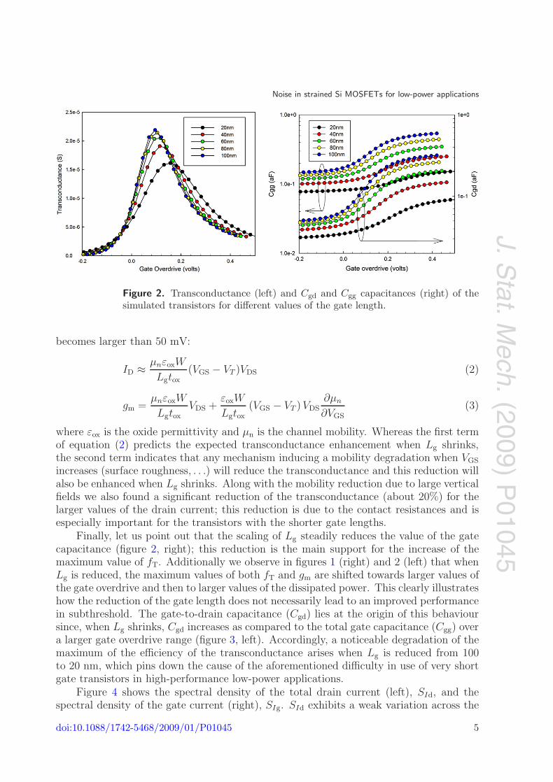
An expected, increase in gm is achieved by decreasing Lg for negative values of thegate overdrive (VGS − Vth) while a noticeable decrease is found for positive values of thegate overdrive (figure 2 left). The latter behaviour is mainly due to the degradation of thechannel mobility. This can be readily understood by obtaining the expression for gm fromthe drain current in the linear region in which the device operates once the gate overdrive
doi:10.1088/1742-5468/2009/01/P01045 4
J.Stat.M
ech.(2009)
P01045
Noise in strained Si MOSFETs for low-power applications
Figure 2. Transconductance (left) and Cgd and Cgg capacitances (right) of thesimulated transistors for different values of the gate length.
becomes larger than 50 mV:
ID ≈ μnεoxW
Lgtox(VGS − VT )VDS (2)
gm =μnεoxW
LgtoxVDS +
εoxW
Lgtox(VGS − VT )VDS
∂μn
∂VGS
(3)
where εox is the oxide permittivity and μn is the channel mobility. Whereas the first termof equation (2) predicts the expected transconductance enhancement when Lg shrinks,the second term indicates that any mechanism inducing a mobility degradation when VGS
increases (surface roughness, . . .) will reduce the transconductance and this reduction willalso be enhanced when Lg shrinks. Along with the mobility reduction due to large verticalfields we also found a significant reduction of the transconductance (about 20%) for thelarger values of the drain current; this reduction is due to the contact resistances and isespecially important for the transistors with the shorter gate lengths.
Finally, let us point out that the scaling of Lg steadily reduces the value of the gatecapacitance (figure 2, right); this reduction is the main support for the increase of themaximum value of fT. Additionally we observe in figures 1 (right) and 2 (left) that whenLg is reduced, the maximum values of both fT and gm are shifted towards larger values ofthe gate overdrive and then to larger values of the dissipated power. This clearly illustrateshow the reduction of the gate length does not necessarily lead to an improved performancein subthreshold. The gate-to-drain capacitance (Cgd) lies at the origin of this behavioursince, when Lg shrinks, Cgd increases as compared to the total gate capacitance (Cgg) overa larger gate overdrive range (figure 3, left). Accordingly, a noticeable degradation of themaximum of the efficiency of the transconductance arises when Lg is reduced from 100to 20 nm, which pins down the cause of the aforementioned difficulty in use of very shortgate transistors in high-performance low-power applications.
Figure 4 shows the spectral density of the total drain current (left), SId, and thespectral density of the gate current (right), SIg. SId exhibits a weak variation across the
doi:10.1088/1742-5468/2009/01/P01045 5

J.Stat.M
ech.(2009)
P01045
Noise in strained Si MOSFETs for low-power applications
Figure 3. Cgd/Cgg ratio (left) and efficiency of the transconductance (gm/Idrain)of the simulated transistors for different values of the gate length.
Figure 4. Spectral density of the total drain current (left) and 1 GHz spectraldensity of the induced gate current (right) for different values of the gate length.
devices studied; its main trend is that the devices with the shorter gate lengths exhibitthe higher levels of SId in the 100 nA–3 μA range. SIg systematically decreases with Lg
(because also the gate area decreases) and with the drain current because the currentconduction is progressively carried away from the oxide interface. The spectral density ofthe total drain current does not explain by itself the significant differences found in theminimum noise figure (NFmin) for low drain currents among the different gate lengths (seefigure 6 below).
To a first approximation, the analysis of the noise figure can be carried out with thehelp of the parameters γ, δ and C of van der Ziel’s model [11]. This model was originallydeveloped using the gradual channel approximation and, therefore, its application to shortchannel MOSFETs faces severe difficulties; nevertheless, in spite of these limitations it
doi:10.1088/1742-5468/2009/01/P01045 6

J.Stat.M
ech.(2009)
P01045
Noise in strained Si MOSFETs for low-power applications
Figure 5. Drain (left) and gate (centre) drain excess noise factor.
Figure 6. Minimum noise figure calculated at 1 GHz for different values of thegate length using the IFM method in 2D.
allows for a quick appraisal of the relative weights of the drain and gate current fluctuationsin the total device noise. The γ parameter at 1 GHz extracted from the simulationfollowing the definition in [12] is presented in figure 5. The remaining two parameters,δ and C, are considerably smaller than γ, and the latter greatly dominates the noisebehaviour of the devices studied in weak inversion. The evolution with the drain currentof the drain excess noise factor (γ parameter) points towards a strong weight of the draincurrent fluctuations in the total noise in the subthreshold region and suggests a growth ofthe drain noise when Lg grows and, thus, it would support the idea that obtaining lower
doi:10.1088/1742-5468/2009/01/P01045 7

J.Stat.M
ech.(2009)
P01045
Noise in strained Si MOSFETs for low-power applications
values of NFmin is possible using transistors with shorter gates. Both in strong and weakinversion, γ deviates from 1 (the equilibrium value) in spite of the small value of the drainbias. In strong inversion, γ grows with the gate bias (drain current) as a result of thedegradation of the channel mobility in short channel/thin oxide transistors.
Figure 6 presents the minimum noise figure at 1 GHz versus the drain current fordifferent values of Lg calculated using the IFM method in the 2D simulation. The NFmin
dependence on Idrain is similar to that of the γ parameter: it exhibits minima located in therange 1–2 μA that correspond to 0.05–0.1 μW in terms of electrical power, the longer gatedevices systematically exhibiting lower values of NFmin for current levels under 2 μA asa direct consequence of a more intense degradation of the channel mobility in the shorterstructures. The NFmin increase when the drain current decreases is related to changes inthe current nature when the transistor leaves the linear region to enter the subthresholdone (this takes place for drain current levels of about 1 μA) and the channel becomesmore resistive (the inverted channel vanishes and transport starts to be barrier limited)and, therefore, the noise must increase accordingly. Barrier-limited transport introducesshot noise. In agreement with this, γ exhibits maxima when the drain current decreasesup to 0.1–0.5 μA as a result of the competition between thermal noise in a more resistivechannel when Idrain is reduced (as explained above) and the onset of the shot noise relatedto the barrier-limited transport. If the drain current decreases further below those levels,0.1–0.5 μA, the noise becomes dominated by the shot one and, accordingly, the values ofγ and NFmin decrease with the drain current.
The noise behaviour discussed for the devices at low drain currents along with thelowering of the efficiency of the transconductance sets up a trade-off between the usualway of increasing fT via gate shortening and the need for low noise and high gm/ID ratiosfor building efficient low-power circuits.
Let us now investigate the effect on noise of the scaling of the oxide thickness. Becausethe above analysis for the scaling of Lg revealed the paramount importance of the gate-to-drain capacitance and total gate capacitance ratio (Cgd/Cgg) for the noise performance,we present in figure 7 (left) the Cgd/Cgg ratio when tox is shrunk from 6 to 2 nm whilemaintaining the remaining parameters of the device unchanged (for instance, the gatelength). This tox reduction only leads to changes in Cgd/Cgg for positive values of the gateoverdrive voltage and, therefore, an aggressive scaling of the oxide thickness will not leadto significant improvements in the performance of the transistor when used in low-powerregimes.
Figure 7 (right) reveals that tox, in good agreement with its above discussed effect onthe Cgd/Cgg ratio, barely modifies NFmin in the subthreshold region. This is in agreementwith the weak effect of the tox scaling on NFmin obtained in simulations (figure 7, right).
Finally, we investigated the effect of the combined scaling of the oxide thickness andthe gate length. This full scaling will substantially leave unmodified the internal values ofthe electric field in the channel. In this case, since there are no p–n junctions at source anddrain contacts (unlike in conventional MOSFETs), in principle the doping profiles in thedevice do not need to be modified during the scaling. Figure 8 gives the impact on NFmin
of the combined scaling when Lg and tox are changed from 60 nm and 6 nm, respectively,to 20 and 2 nm. The combined scaling leads to similar behaviours for moderate currentlevels in the three structures, and partly mitigates the increase in NFmin encountered atlow current levels (subthreshold regime) when only the gate length is scaled (figure 4).
doi:10.1088/1742-5468/2009/01/P01045 8

J.Stat.M
ech.(2009)
P01045
Noise in strained Si MOSFETs for low-power applications
Figure 7. Cgd/Cgg ratio (left) and minimum noise figure (right) for the simulatedtransistors for different values of the oxide thickness.
Figure 8. Minimum noise figure of the fully scaled devices.
4. Conclusions
A theoretical study of the thermal noise in strained n-channel Si/SiGe MOSFETs ispresented. The study was carried out using a 2D device simulator based on thehydrodynamic model and the impedance field method, to self-consistently obtain thecurrent noise at the device’s terminals. The analysis focused on the possible benefits ofthe scaling on the AC and noise performance of the transistor for low-power applications.A pure scaling of the transistor’s gate length is detrimental to subthreshold operation interms of the minimum noise figure (NFmin), but would lead to lower values of NFmin formedium and high current levels. Scaling the oxide thickness would not affect NFmin in
doi:10.1088/1742-5468/2009/01/P01045 9

J.Stat.M
ech.(2009)
P01045
Noise in strained Si MOSFETs for low-power applications
subthreshold operation, but it will be detrimental for medium and high current levels.A combined scaling of the oxide thickness and the gate length mitigates the degradationof NFmin in subthreshold operation when the device geometry shrinks, at the cost ofeliminating the NFmin reduction related to the shortening of the gate length at highercurrent levels.
Acknowledgment
This work received financial support from MEC-FEDER under the grant (TEC2005-02719/MIC).
References
[1] Zeuner M et al , 2003 Japan. J. Appl. Phys. 42 2363[2] Olsen S H, O’Neill A G, Driscoll L S, Kwa K S K, Chattopadhyay S, Waite A M, Tang Y T, Eva A G R,
Norris D J, Cullis A G, Paul D J and Robbins D J, 2003 IEEE Trans. Electron Devices 50 1961[3] Galan J, Carvajal R G, Torralba A, Munoz F and Ramırez-Angulo J, Fellow , 2005 IEEE Trans. Circuits
Syst. I 52 283Vilches A, Fobelets K, Michelakis K, Despotopoulos S, Papavassiliou C, Hackbarth T and Konig U, 2003
IEE Electron. Lett. 39 884Serra-Graells F and Huertas J L, 2005 IEEE Trans. Circuits Syst. I 52 2090
[4] Aniel F, Enciso-Aguilar M, Giguerre L, Crozat P, Adde R, Mack T, Seiler U, Hackbarth Th, Herzog H J,Konig U and Raynor B, 2003 Solid-State Electron. 47 283
[5] Fobelets K, Jeamsaksiri W, Papavasilliou C, Vilches T, Gaspari V, Velazquez-Perez J E, Michelakis K,Hackbarth T and Konig U, 2004 Solid-State Electron. 48 1401
[6] Bakker A, Thiele K and Huijsing J H, 2000 IEEE J. Solid-State Circuits 35 1877[7] 2002 Medici User’s Manual (Fremont, CA: Synopsys TCAD Business Unit)[8] Martın M J, Pardo D and Velazquez J E, 1998 J. Appl. Phys. 84 5012[9] Martın M J, Pardo D and Velazquez J E, 1999 Physica B 272 263
[10] Dollfus P, Bournel A and Velazquez-Perez J E, 2006 J. Comput. Electron. 5 479[11] van der Ziel A, 1986 Noise in Solid State Devices and Circuits (New York: Wiley)[12] Lee T H, 2004 The Design of CMOS Radio-Frequency Integrated Circuits (Cambridge: Cambridge
University Press)
doi:10.1088/1742-5468/2009/01/P01045 10
Copyright © 2022 FDOKUMEN