CNT/Graphite/SBS Conductive Fibers for Strain Sensing in ...
Upload
independentCategory
view
5download
0
Quantum Modeling and Design ofCarbon Nanotube (CNT) Embedded
Nanoscale MOSFETs
Akin Akturk, Gary Pennington and Neil Goldsman
Department of Electrical and Computer EngineeringUniversity of Maryland, College Park, MD 20742, USA
[email protected], [email protected],[email protected]
Abstract
We propose a novel MOSFET design that embodies single wall
zig-zag semiconducting Carbon Nanotubes (CNT) in the
channel, as shown in Fig. 1. Investigations show that CNTs
have high low-field mobilities, which can be as great as
2x105 cm2/Vs. Thus we predict that MOSFET performance can be
improved by embedding CNTs in the channel. To investigate
the performance of the new CNT-MOSFET device, we develop a
methodology that connects CNT modeling to MOSFET
simulations. Our calculations indicate that by forming high
mobility regions in the channel, MOSFET performance can be
boosted. The gain in the drive current is as much as 30-40%
over standard MOSFETs. Our predictions are based on
calculations obtained from our CNT Monte Carlo (MC)
simulator [1]-[3] and quantum based device solver [4]-[6].

Keywords: Single-Wall Zig-Zag Carbon Nanotube, CNT Mobility
Model, CNT Embedded MOSFET Design, Simulation.
I-Introduction:
As we approach the end of the semiconductor roadmap,
investigators are exploring device technologies to push
electronics into the 21st century. Carbon nanotubes (CNTs)
are being explored as a structure that may play a leading
role in future electronic systems. CNTs are planar graphite
sheets (graphene) that are seamlessly wrapped into tubes, as
shown in Fig. 2. CNTs possess favorable electrical
characteristics and can be fabricated in dimensions as small
as 4-8Å in diameter. The electrical characteristics of a CNT
vary with its diameter and the wrapping angle of the
graphene [7]. Both the diameter and the wrapping angle can
be described by the tube’s fundamental indices (n,m). Theory
indicates that CNTs can be metallic or semiconducting
depending on the fundamental tube indices (n,m), and bandgap
depends on the diameter. Analysis shows semiconducting CNTs
have very high low-field mobilities, with peak drift
electron velocities that can be as much as five times higher
than that of silicon. It has also been shown that tubes can
be doped by donors and acceptors [7,8]. Experiments and
calculations also indicate that CNTs could facilitate
devices with large transconductances and high drive currents
[4,5], [7]-[15]. Experiments have demonstrated the viability
of CNT-based FETs [12,13], and CNT-SOI type MOSFETs [14,15].
Preliminary research has been done to model, design CNT
embedded bulk MOSFETs [4,5],
We propose a novel CNT-MOSFET device that is shown in
Fig. 1. Our calculations indicate that the CNT-MOSFET can
have improved device performance over the conventional
MOSFET [4,5]. To investigate the potential attributes of the
new design, we developed a methodology for modeling
nanoscale CNT-MOSFETs. It includes determination of the
electrical characteristics of single wall zig-zag CNTs, and
the merging of the CNT results into our quantum device
solver. To electrically characterize the CNT, we developed a
Monte Carlo (MC) simulator for CNTs. We first calculate
electron and phonon dispersion relations for single wall
zig-zag CNTs with different tube indices n. We then derive
the selection rules and scattering matrix elements, using
Fermi’s Golden Rule. Using MC results, we derive analytical
models for CNT parameters such as mobility and density of
states. Once we obtain CNT parameters, we import them to our

quantum device solver. Our device solver is based on the
semiconductor equations, modified to account for quantum
effects, and the Schrödinger equation. We solve these
coupled equations on a discretized mesh of our CNT-MOSFET
device shown in Fig. 1. The solution gives results which
include: CNT-MOSFET current voltage curves, electron
concentration profile, in the bulk MOSFET, and in the CNT
enhanced channel.
We summarize our algorithm in Fig. 3.
II-CNT Simulator:
As mentioned above, we first employ a Monte Carlo (MC)
simulator [1]-[3] to characterize fundamental transport
properties of CNTs, and then we incorporate these properties
into our device simulator. These properties include electron
drift velocity versus electric field curves as well as CNT
mobility for zig-zag single wall CNTs, which is the most
studied topology. To obtain these properties, we begin with
the physical CNT system, where electrons are confined around
the circumference, and move relatively freely along the tube
in the direction of the longitudinal axis. Therefore, one
can write the appropriate plane wave solutions that satisfy
periodicity for the given CNT circumference. However along
the tube, electrons are not confined. Thus the wavevector
can be written as follows:
, ( ) (1)
Here is parallel to the tube axis, and is the unit
vector along the circumference. Discrete values around the
circumference, β, are bounded by the fundamental tube index
n, to take advantage of the symmetry lines in the CNT
Brillouin zone. Note that n count as one unique zone
boundary. A zig-zag single wall CNT and its corresponding
Brillouin zone can be found in Figs. 2 and 4, respectively.
We consider one-dimesional semiclassical charge transport
along the tube.
As external field is applied, electrons are accelerated
along the tube up until they scatter with phonons. Here we
consider scattering by optical, and acoustic inter and intra
subband, and intervalley. Both scattering mechanisms are
treated within the deformation potential approximation using
the Fermi’s Golden Rule. In this work, we use 3eV and 9eV
for the nearest-neighbor π-hopping integral and the
deformation potential, respectively. For more details of our
MC simulations we refer the reader to [1,2].
A. CNT Bandstructure:
To account for the CNT related quantum effects in the CNT-
MOSFET channel, we need to determine the band-structure of
the CNTs. Due to confinement, the bandstructure splits into
a system of subbands when graphene is wrapped into a CNT.

Each of the subbands has a characteristic effective mass,
mobility and band energy minima.
We determine the energy levels of CNTs by applying zone-
folding methods to graphene. From the two-dimensional
graphene band diagram, we cut one-dimesional slices, whose
numbers and locations are set by the fundamental tube
indices (n,m).
We use zone-folding of the graphene conduction band to
calculate the electronic bandstructure of CNT. The following
formula gives the energy dispersion for a zig-zag CNT[7]:
(eV) (2)
Where a (=2.46Å) is the lattice constant of two dimensional
graphite. It has been shown that this analytical formula
agrees with experimental results [7].
To extract the pertinent information that can be easily
integrated into our device simulator, we transform Eqn. (2)
into a quadratic form which is consistent with traditional
semiconductor analysis:
However we use a parabolic energy bandstructure, instead of
the one in Eqn. 2. Because it is too complicated for use in
an MC code and the parabolic dispersion curves well
approximate the tight-binding bandstructure for energies of
our interest, which is up to 2eV above the conduction band

minimum. In Fig. 5, we show how well the parabolic
bandstructure fits the results of the tight-binding model.
The parabolic energy dispersion relation for different
subbands can be written as follows:
(3)
Here is the conduction band minimum, is the
parabolicity factor, and is the effective mass in
subband β for a tube with index n. Conduction band minimum,
effective mass and parabolicity factor can be calculated
using Eqn. 2 for different subbands. For example, conduction
band minimum for each subband can be found by setting kx to
zero in Eqn. 2, and choosing the appropriate signs for the
expression below such that E is minimum:
(eV) (4)
Likewise, effective mass is the curvature of the energy
dispersion relation given in Eqn. 2 around kx=0. We obtain
the following formula for the effective masses of each
subband:
(5)
Our calculations indicate that only the lowest three
subbands are effective in the electron transport
calculations along the tube. Thus we only deal with those

subbands, which correspond to βo, 2(n-βo), and 2(2βo-n),
where βo is equal to 2n/3 rounded to the nearest integer.
They are written in an order starting from the subband that
has the lowest energy minimum and increasing. Note that
these subbands are not around the gamma point, but rather
correspond to higher frequencies. In Table 1, we give a list
of conduction band minimums and effective masses for the
first three subbands of different tubes.
B. CNT Mobility Model:
We derived a mobility model based on our MC simulation
results of drift velocity versus electric field curves. They
are plotted in Fig. 6 for CNTs with tube indices 10 to 58.
They are equivalently ranging in diameter from 8Å to 46Å.
Simulation indicates that electron drift velocity first
increases linearly with the applied field, reaches a
maximum, and then rolls off, showing a negative differential
mobility (NDM). We find that peak electron velocities are as
much as four times higher than what they are in silicon.
Electrons reach velocities as high as 5x107cm/s in large
diameter CNTs (n=58), while the maximum velocity, which is
approximately 3x107cm/s for n=10, drops for smaller diameter
tubes. However this is still larger than the corresponding
values in other semiconductors. Calculated results also show
that the critical field, where we have the peak drift
velocity, increases from 1kV/cm to 10kV/cm as we enlarge the
tube diameter from 8Å to 46Å.
Figure 6 shows three main characteristics of the CNTs.
First, CNTs attain larger drift velocities than other
semiconductors. Investigations show that is due to decreased
scattering rates, which is a result of the one-dimensional
system we have. Second, electrons in large diameter tubes
have higher velocities than the ones in small diameter tubes
for a given applied field, unless the applied field is too
large. This leads to higher low-field mobilities for larger
diameter tubes. Analysis show that is due to increased
density of states of the large diameter tubes. Third, all
CNTs show NDM. It is similar to GaAs in that respect, where
conduction band velocity of the first subband is larger than
that of the second.
We develop an analytical mobility model considering the two
lowest subbands, which dominate the conduction. By that
means, we embed the effects of NDM in our model. We then
express the final mobility using Mathiessen’s rule, as
follows:
(6)

Where and refer to the mobilities in the
first and second subbands, respectively. They are functions
of fundamental tube index, n, and the electric field, F. The
mobility of the first subband is:
(7)
Here is the low-field mobility, and Fc(n) is the
critical electric field. The critical electric field
corresponds to the peak electron drift velocity. We have the
following expressions for the low-field mobility and the
critical field:
, (cm2/Vs) (8)
, (V/cm) (9)
Here ρ=1-gcd(n+1,3) (= 0, -2), where gcd(n+1,3) is the
greatest common divisor of n+1 and 3.
We can write the mobility of the second subband as follows:
, (V/cm) (10)
Here Vmax is the maximum drift velocity of the electrons,
shown in Fig. 6. It is formulated below as:
, (cm/s) (11)
In Fig. 7, we show our calculated mobility versus field
curves, using Eqns. 6-11. CNTs can sustain large mobilities,
larger than all known semiconductor devices. For n=58, low-
field mobility is as high as 2x105cm2/Vs, while for n=10 it
is approximately 4x103cm2/Vs. So they can be used to form
high mobility regions.
C. CNT Intrinsic Carrier Concentration:
To embed a CNT in our device solver, we need a value for the
intrinsic carrier concentration of the CNT. Thus we develop
a methodology to obtain the intrinsic concentrations of
different tubes. We start from the parabolic energy
dispersion relation in Eqn. 3. However we ignore the
parabolicity factor to simplify calculations. The density of
states for each subband is:
(12)
We also assume that we have a Maxwellian type distribution.
Thus we get the following expression for the intrinsic
carrier concentration, where Fermi level is set to zero:
(13a)
Or equivalently:

(13b)
The integral in Eqn. 13b can be recognized as the gamma
function with an argument equal to ½, and integral is equal
to . The expression in Eqn. 13 gives one-dimensional
carrier concentration, whereas we need the concentration per
volume. Thus we further assume that the vertical cross
section of the tube can be fit in a square, whose side is
one diameter long. Finally, we arrive at the following
formula for the intrinsic carrier concentration, which is
only a function of fundamental tube index n:
(14)
III-Quantum Device Simulator:
We develop a quantum device solver [4]-[6] based on the
Schrödinger equation and drift-diffusion equations. They are
listed below in the order of Schrödinger, Poisson, electron
current-continuity, hole current continuity and lattice heat
flow equations.

(15)
(16)
(17)
(18)
(19)
Here the newly introduced variables , ψ, n-p, Jn-p, T, D,
GRn-p, C and κ are electrostatic potential, wave function,
electron-hole concentrations, electron-hole current
densities, lattice temperature, net dopant concentration,
electron-hole net generation-recombination rates, heat
capacity and thermal diffusion constant, respectively. In
Eqn. 15, x is parallel to the Si-SiO2 interface in MOSFET,
and y is normal to x.
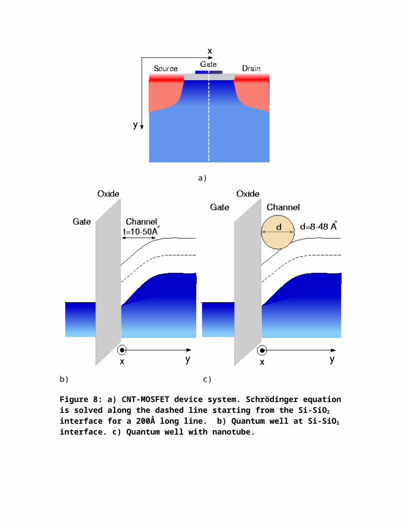
Solution of the CNT-MOSFET system requires proper handling
of two dynamics. First one is the quantum well formed at the
Si-SiO2 interface that causes band splitting thus lowering
of the carrier concentration. Second one is the
heterojunction formed at the CNT-silicon interface that
reflects the different bandstructures of the CNT and
silicon.

We first solve our system classically. This includes the
coupled solution of Eqns. 16-19. At this stage, we also
resolve the effects of heterostructure, through the use of a
revised Scharfetter-Gummel discretization scheme. The
details can be found in [4]. We keep the Scharfetter-Gummel
discretization intact, but modify electron current density
as follows:
(20)
Here no(x,y) is the intrinsic carrier concentration at a
grid point on our device, and is the intrinsic carrier
concentration of silicon.
Investigations show that carrier confinement at the Si-SiO2
interface can significantly reduce carrier concentration
adjacent to the interface [15]. Thus we also solve for the
quantum effects using the classical solution as our initial
guess. To inherent quantum effects in our device model, we
solve the Schrödinger equation, Eqn. 15, in addition to
Eqns. 16-19. We solve the one-dimensional Schrödinger
equation along the normal direction of Si-SiO2 interface,
starting from the interface and going down the substrate
about 200Å. We apply the same procedure to different mesh
points along x in the channel, as well. The physical system
and the quantum well can be found in Fig. 8.

We treat the quantum induced effects like the formation of
position dependent heterostructures in the quantum well.
Thus we sum quantum effects in the carrier concentration
term, where quantum confinement is reflected as bandgap
broadening. This methodology introduces an extra term within
the parentheses of the gradient in Eqn. 20, as follows:
(21)
Here subscripts refer to quantum (QM) and classical (CL)
solutions. We calculate the quantum carrier concentration
using the solution of the Schrödinger equation, which gives
energy eigenvalues and eigenfunctions. We then combine the
resulting subband structure with the occupation densities,
which can be seen in Fig. 9. Thus we get the following
formula for the quantum carrier concentration, where we have
a sum over different subbands:
(22)
In summary, we first solve the coupled Poisson, electron
current continuity, hole current continuity and heat flow
equations, classically. During the simulation, we also
include the effects of the heterostructure formed by the CNT
and silicon. We achieve this by using an effective
potential, argument of the gradient in Eqn. 20, instead of
the classical electrostatic potential, , in the drift-
diffusion equations. After we have the coupled solution of
the device equations, we use it as an initial guess for the

quantum system. We iteratively solve Schrödinger, Poisson,
quantum electron and hole current continuity, and heat flow
equations until coupled solution of the Schrödinger equation
and quantum electron current continuity equation give the
same electron concentration. Carrier concentration using the
solution of the Schrödinger equation is calculated as shown
in Eqn. 22. Whereas we get the carrier concentration within
the modified drift-diffusion (DD) formalism as follows:
(23)
Here noQM(x,y) is the intrinsic carrier concentration at a
grid point on our device, that includes the effects of the
heterostructure, as well as the quantum.
Once we have the coupled solution of the system, our quantum
device solver outputs current-voltage curves, and profiles
of quantum electron concentration, electrostatic potential,
hole concentration and such. In Fig. 10, we show our
calculated electron concentration in the vertical direction
of the MOSFET channel, starting from the Si-SiO2 interface.
We applied 0.7V to the gate terminal, and grounded others.
CNT-MOSFETs with large diameter tubes have higher
concentrations in the channel. Thus they are likely to
sustain large transconductances but may be at the expense of
weaker isolation in the “off” state of the MOSFET. We also
obtain the current-voltage characteristics of the 0.1μm CNT-
MOSFETs in the linear and saturation regions. We show the

drain current density versus applied drain voltage curves in
Fig. 11. There are three configurations for comparison.
First one is the conventional MOSFET without any CNTs in the
channel. The other two are the CNT-MOSFETs with small (8Å)
and large (46Å) diameter CNTs in the MOSFET channel. We find
that CNT-MOSFETs utilizing smaller diameter tubes attain
higher drive currents than the ones having larger diameter
tubes, followed by the conventional MOSFET. The ordering
within CNT-MOSFETs can be attributed to the height of the
barrier formed at the CNT-silicon heterojunction. However
they both have improved drive current characteristics than
the conventional MOSFET due to larger channel electron
concentrations shown in Fig. 10 and larger mobility values
on CNTs. In Fig. 12, we plot the subthreshold
characteristics of these three devices. Large diameter tubes
have higher leakage currents than others, making them
undesirable for low power applications. However small
diameter tubes give rise to improved performance in
subthreshold, linear and saturation regions, making them
favorable for low power and high frequency applications.
IV-Conclusion:
We propose a novel device structure that combines the MOSFET
technology with CNT nanostructures. We report on our
predictions that the CNT-MOSFET device is likely to have
better performance than the conventional MOSFET. To analyze
the new design, we develop a methodology for
modeling and simulating CNTs and CNT-MOSFETs. We first
employ MC techniques to electrically characterize single
wall zig-zag CNTs. For MC calculations, we obtain the energy
dispersion relation and the phonon spectrums of CNTs by
applying zone-folding methods to graphite. We derive
selection rules and scattering rates from Fermi’s Golden
rule. We also include collision broadening effects. We then
derive analytical models for CNT parameters like mobility.
We import these results to our quantum device solver and
determine the current-voltage characteristics of CNT-
MOSFETs. We predict that the drive current of CNT-MOSFETs is
higher than the conventional MOSFETs, with the smaller
diameter tube has the highest. Likewise in the subthreshold
region, narrow diameter tube has the best performance. Thus
we predict that CNT-MOSFETs employing lower diameter tubes
are likely to have good device performance and can be used
in low power and high frequency devices.

Figure 1: Simulated CNT-MOSFET device.

Figure 2: Simulated zig-zag single wall CNT structure.


Figure 3: Coupled algorithm flowchart.

Figure 4: CNT Brillouin zone on graphene k-space. x is alongthe tube axis, and θ refers to the circumference. High symmetry directions of ΓMK are also shown.

Figure 5: Bandstructure for a zig-zag CNT with n=10. Solid and dashed lines refer to parabolic and tight-binding bandstructures, respectively. Inset is for n=59.

Figure 6: Electron drift velocity versus electric field curves for zig-zag CNTs with different tube indices.


Figure 7: Calculated mobility versus electric field curves for zig-zag CNTs with different tube indices.
a)
b) c)
Figure 8: a) CNT-MOSFET device system. Schrödinger equation is solved along the dashed line starting from the Si-SiO2 interface for a 200Å long line. b) Quantum well at Si-SiO2 interface. c) Quantum well with nanotube.

a)
b)
Figure 9: a) Quantum well at the Si-SiO2 interface causes band splitting. b) We calculate the quantum carrier concentration by summing charges in different subbands, weighted by the density of states, D(E), and the probabilityof finding a carrier.

0 1 2 3 4
1017
1018
1019
Vertical (nm )
Electron Co
ncentration (1/cm
3 )
Figure 10: Calculated electron concentration in the verticaldirection of the Si-SiO2 interface. Marked line is for CNT-MOSFET with a large diameter CNT (46Å). For the other twocurves, the one that has slightly higher concentrationaround 0.5nm is for CNT-MOSFET with a small diameter tube(8Å). The remaining one is for the conventional MOSFET.

Figure 11: Calculated current-voltage curves. CNT-MOSFETs show 30-80% increase in drain current. We applied gate biases of 0.4V, 0.7V, and 1.0V.
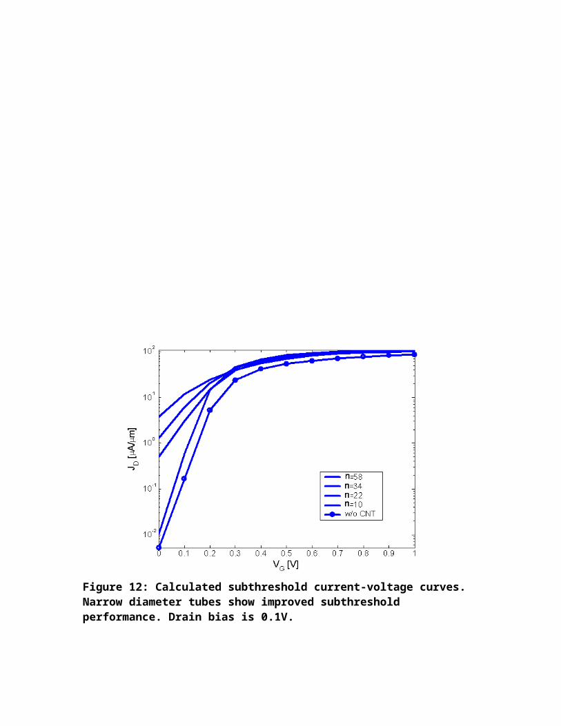
Figure 12: Calculated subthreshold current-voltage curves. Narrow diameter tubes show improved subthreshold performance. Drain bias is 0.1V.

Table 1: Band structure parameters for zig-zag CNTs.
n (m=0) Band (eV) ( ) β
10 1 0.086 0.527 72 0.358 1.146 63 0.221 1.854 8
22 1 0.043 0.244 152 0.118 0.507 143 0.137 0.929 16
34 1 0.029 0.159 232 0.070 0.326 223 0.099 0.616 24
58 1 0.017 0.093 392 0.039 0.189 38

3 0.063 0.367 40
V. References
[1] G. Pennington, N. Goldsman, “Semiclassical Transport and
Phonon Scattering on Electrons in Semiconducting Carbon
Nanotubes,” Phys. Rev. B, vol. 86, pp. 45426-37, 2003.
[2] G. Pennington, N. Goldsman, “Monte Carlo Study of
Electron Transport in a Carbon Nanotube,” IEICE Trans. Electron.,
vol. E86-C, pp. 372-8, 2003.

[3] G. Pennington, A. Akturk, and N. Goldsman, “Drift
Velocity and Mobility Model for Carbon Nanotubes,” IEEE Elect.
Dev. Lett, “submitted for publication”.
[4] A. Akturk, G. Pennington, and N. Goldsman, “Modeling the
Enhancement of Nanoscale MOSFETs by Embedding Carbon
Nanotubes in the Channel,” Third IEEE Conf. on Nanotech., pp. 24-
7, 2003.
[5] Akturk, G. Pennington, and N. Goldsman,
“Characterisation of Nanoscale Carbon Nanotube (CNT)
Embedded CMOS Inverters,” ISCAS 2004, “submitted for
publication”.
[6] A. Akturk, N. Goldsman, G. Metze, “Increased CMOS
Inverter Switching Speed with Asymmetrical Doping,” Solid-State
Electronics, vol. 17, no. 2, pp. 185-92, 2003.
[7] R. Saito, M. S. Dresselhaus, and G. Dresselhaus,
Physical Properties of Carbon Nanotubes, Imperial College
Press, London, 1998.
[8] R. S. Lee, H. J. Kim, J. E. Fischer, A. Thess, R. E.
Smalley, “Conductivity Enhancement in Single-Walled Carbon
Nanotube Bundles Doped with K and Br,” Nature, vol. 388, pp.
255-7, 1997.

[9] L. Grigorian, G. U. Sumanasekera, A. L. Loper, S. Fang,
J. L. Allen, and P. C. Eklund, “Transport Properties of
Alkali-Metal-Doped Single-Wall Carbon Nanotubes,” Phys. Rev.
B, vol. 58, pp. R4195-8, 1998
[10] Z. Yao, C. L. Kane, and C. Dekker, “High-Field
Electrical Transport in Single-Wall Carbon Nanotubes,” Phys.
Rev. Lett, vol. 84, pp. 2941-4, 2000.
[11] J. Hone, M. Whitney, C. Piskoti, and A. Zettl, “Thermal
Conductivity of Single-Walled Carbon Nanotubes,” Phys. Rev. B,
vol. 59, pp. R2514-6, 1999.
[12] A. Bachtold, P. Hadley, T. Nakanishi, and C. Dekker,
“Logic Circuits with Carbon Nanotube Transistors,” Science,
vol. 294, pp. 1317-20, 2001.
[13] R. Martel, V. Derycke, J. Appenzeller, S. Wind, Ph.
Avouris, “Carbon Nanotube Field-Effect Transistors and Logic
Circuits,” IEEE Design Automation Conf., pp. 94-8, 2002.
[14] S. J. Tans, A. R. M. Verschueuren, and C. Dekker, “Room
Temperature Transistor Based on a Single Carbon Nanotube,”
Nature, vol. 393, pp. 49-52, 1998.

[15] S. J. Wind, J. Appenzeller, R. Martel, V. Derycke, Ph.
Avouris, “Vertical Scaling of Carbon Nanotube Field-Effect
Transistors using Top Gate Electrodes,” Applied Physics Letter,
vol. 80, no. 20, pp. 3817-9, 2002.
[16] C. K. Huang, and N. Goldsman, “2-D Self-Consistent
Solution of Schrödinger Equation, Boltzmann Transport
Equation, Poisson and Current-Continuity Equation for
MOSFET,” SISPAD 2001, pp. 148-51, Spring-Verlag, 2001.
Copyright © 2022 FDOKUMEN